EP1068632B1 - Contamination controlling method and plasma processing chamber - Google Patents
Contamination controlling method and plasma processing chamberDownload PDFInfo
- Publication number
- EP1068632B1 EP1068632B1EP99915049AEP99915049AEP1068632B1EP 1068632 B1EP1068632 B1EP 1068632B1EP 99915049 AEP99915049 AEP 99915049AEP 99915049 AEP99915049 AEP 99915049AEP 1068632 B1EP1068632 B1EP 1068632B1
- Authority
- EP
- European Patent Office
- Prior art keywords
- liner
- processing chamber
- plasma
- exposed surface
- silicon carbide
- Prior art date
- Legal status (The legal status is an assumption and is not a legal conclusion. Google has not performed a legal analysis and makes no representation as to the accuracy of the status listed.)
- Expired - Lifetime
Links
Images


Classifications
- H—ELECTRICITY
- H01—ELECTRIC ELEMENTS
- H01J—ELECTRIC DISCHARGE TUBES OR DISCHARGE LAMPS
- H01J37/00—Discharge tubes with provision for introducing objects or material to be exposed to the discharge, e.g. for the purpose of examination or processing thereof
- H01J37/32—Gas-filled discharge tubes
- H—ELECTRICITY
- H01—ELECTRIC ELEMENTS
- H01J—ELECTRIC DISCHARGE TUBES OR DISCHARGE LAMPS
- H01J37/00—Discharge tubes with provision for introducing objects or material to be exposed to the discharge, e.g. for the purpose of examination or processing thereof
- H01J37/32—Gas-filled discharge tubes
- H01J37/32431—Constructional details of the reactor
- H01J37/32458—Vessel
- H01J37/32477—Vessel characterised by the means for protecting vessels or internal parts, e.g. coatings
- H—ELECTRICITY
- H01—ELECTRIC ELEMENTS
- H01J—ELECTRIC DISCHARGE TUBES OR DISCHARGE LAMPS
- H01J37/00—Discharge tubes with provision for introducing objects or material to be exposed to the discharge, e.g. for the purpose of examination or processing thereof
- H01J37/32—Gas-filled discharge tubes
- H01J37/32009—Arrangements for generation of plasma specially adapted for examination or treatment of objects, e.g. plasma sources
- H01J37/32082—Radio frequency generated discharge
- H01J37/321—Radio frequency generated discharge the radio frequency energy being inductively coupled to the plasma
- H—ELECTRICITY
- H01—ELECTRIC ELEMENTS
- H01J—ELECTRIC DISCHARGE TUBES OR DISCHARGE LAMPS
- H01J2237/00—Discharge tubes exposing object to beam, e.g. for analysis treatment, etching, imaging
- H01J2237/02—Details
- H01J2237/022—Avoiding or removing foreign or contaminating particles, debris or deposits on sample or tube
Definitions
- the inventionrelates to improvements in a plasma processing chamber and to a method of processing a substrate in the plasma processing chamber such as by plasma etching an oxide layer on a semiconductor wafer.
- Vacuum processing chambersare generally used for chemical vapor depositing (CVD) and etching of materials on substrates by supplying process gas to the vacuum chamber and application of an RF field to the gas.
- CVDchemical vapor depositing
- ICPtransformer coupled plasma
- ECRelectron-cyclotron resonance
- substrate holdersinclude mechanical clamps and electrostatic clamps (ESC). Examples of mechanical clamps and ESC substrate holders are provided in commonly owned U.S, Patent No. 5,262,029 and commonly owned U.S. Patent No. 5,671,116 filed on March 10, 1995.
- Substrate holders in the form of an electrodecan supply radiofrequency (RF) power into the chamber, as disclosed in U.S. Patent No. 4,579,618.
- RFradiofrequency
- metal surfaces of wafer support and clamping ring mechanismscan be covered with insulating material to prevent erosion by the plasma and electrically conductive material can be used to reduce arcing due to charge build-up on such insulation surfaces.
- Plasma processing systemswherein an antenna coupled to a radio frequency (RF) Source energize gas into a plasma state within a process chamber are disclosed in US Patent No's 4,948,458; 5,198,718; 5,241,245 and 5,401,350.
- the antennais located outside the process chamber and the RF energy is supplied to the chamber through a dielectric window.
- Such process systemscan be used for a variety of semiconductor processing applications such as etching, deposition, resist stripping, etc.
- EP-A-0 821 397discloses a silicon carbide composite article particularly useful for plasma reactors and exhibiting steps and components corresponding to those recited in the precharacterising parts of claims 1 and 12 herein.
- An object of the inventionis to reduce metal and/or particle contamination of plasma processed substrates when substrates are processed continuously.
- US-A-5,085,727describes a method of processing a substrate and a process chamber for carrying out the method.
- the present inventionprovides a method of processing a substrate according to claim 1.
- the processing chambercan include a substantially planar antenna and the process gas can be energised into the plasma state by supplying RF power to the antenna.
- the plasmacan comprise a high density plasma and the substrates can be processed by etching an oxide layer on the substrates with the high density plasma while supplying an RF bias to the substrates.
- At least one further exposed surface composed of a silicon carbide based materialcan be provided and in this case the further surface is defined by a gas distribution plate supplying the process gas to the process chamber, a perforated baffle extending between the substrate holder and the liner and/or the focus ring surrounding the substrate.
- the liner the distribution plate the baffle and/or the focus ringconsist essentially of hot-pressed sintered , CVD or reaction bonded SiC or a composite wherein a coating of SiC forms the exposed surface thereof
- the chambercan further include a dielectric window adjacent the gas distribution plate and the RF energy source or planar antenna can be adjacent the window to supply power through the window to energize the process gas in the processing chamber into a plasma state.
- the antennacan be arranged such that the gas outlets in the gas distribution plate are not directly between the substrate holder and the antenna.
- the dielectric windowcan have a substantially uniform thickness and substantially planar configuration and the gas distribution plate can have a substantially uniform thickness and substantially planar configuration.
- high density plasmastypically cause a relatively high erosion rate of chamber interior surfaces they contact due to physical and/or chemical sputtering. This is an important issue in applications for wafer processing in the semiconductor industry, due to the sensitivity of devices on the wafer to contamination from metals which are deep impurities in silicon such as nickel and iron, alkali metals such as sodium and potassium that are mobile ions in the gate oxide of devices causing unstable threshold voltage, and metals such as aluminum which cause leakage currents in device junctions resulting, for example, in short refresh times in DRAM memory cells. Because of this, the surfaces of the chamber exposed to the high density plasma in such wafer processing tools are normally covered with a nonmetallic material such as alumina or quartz.
- Alumina and quartzare dielectric materials which present a high impedance to the RF current used to sustain the plasma, and the RF current used to induce a bias voltage on the wafer.
- the RF current through the plasmadoes not have a good ground path and can become unstable, resulting in non-repeatable etch results.
- charge build-up on the dielectric materialscan cause arcing and thus localized sputtering of the dielectric materials.
- the present inventionuses a liner acting as a side wall of the processing chamber as a separate component with a surface of silicon carbide (SiC) as a consumable chamber surface material which reduces metal and/or particle contamination of the processed substrates.
- the liner componentis electrically conductive so that when it is in contact with the plasma it presents a good ground path for the RF current.
- the SiC linerprovides a grounded surface which is resistant to erosion from ion bombardment and reduces plasma potential on surfaces in the chamber.
- the linercan consist entirely of SiC, comprise a SiC coated material such as SiC coated graphite, or principally SiC with 10 to 20% Si added to fill porosity in reaction bonded SiC.
- the SiCalso etches at a slow rate by the plasma making the component a cost effective consumable part. Moreover, because the SiC is of high purity, wafer contamination resulting from chemical sputtering of the SiC by the plasma can be minimized. Further, the grounded SiC liner component can reduce sputtering of other surfaces in the chamber by causing a reduction in the plasma potential and hence ion bombardment energy to these non-silicon carbide surfaces. To the extent the SiC component replaces alumina as a chamber surface, aluminium contamination of wafers can be reduced. Finally, the SiC component provides a very stable plasma potential so that etch results are more repeatable within an individual chamber and from chamber to chamber.
- the inventionprovides improvements in reducing contamination of substrates such as semiconductor wafers, flat panel display substrates, and the like.
- the reduced contaminationcan be enhanced by utilizing silicon carbide as the material for additional members with exposed surfaces adjacent the substrate being processed in the chamber.
- additional membersinclude non-electrically driven chamber parts such as focus rings, gas distribution plates, baffle plates and the like.
- the linercan provide a better RF return path for the powered electrode (bottom electrode) in the wafer support.
- a gas distribution platecan be used to control the spatial distribution of gas flow in the volume of the reactor above the plane of the wafer.
- the gas distribution plateis a circular plate situated directly below the TCPTM window which is also the vacuum sealing surface at the top of the reactor in a plane above and parallel to the wafer.
- the gas distribution plateis sealed using an O-ring to a gas distribution ring located at the periphery of the gas distribution plate.
- the gas distribution ringfeeds gas from a source into the volume defined by the gas distribution plate, an inside surface of a window underlying a coil supplying RF energy into the reactor, and the gas distribution ring.
- the gas distribution platecontains an array of holes of a specified diameter which extend through the plate.
- the spatial distribution of the holes through the gas distribution platecan be varied to optimize etch uniformity of the layers to be etched, e.g., a photoresist layer, a silicon dioxide layer and an underlayer material on the wafer.
- the cross-sectional shape of the gas distribution platecan be varied to manipulate the distribution of RF power into the plasma in the reactor.
- the gas distribution plate materialmust be a dielectric to enable coupling of this RF power through the gas distribution plate into the reactor.
- the material of the gas distribution platemust be highly resistant to chemical sputter-etching in environments such as oxygen or a hydrofluorocarbon gas plasma in order to avoid breakdown and the resultant particle generation associated therewith. Moreover, the material of the gas distribution plate should have low levels of contaminants that might otherwise affect performance of devices on the wafer. According to a preferred embodiment of the invention, the gas distribution plate can be of specially prepared silicon carbide having high resistivity.
- FIG. 1A vacuum processing chamber according to one embodiment of the present invention is illustrated in FIG. 1.
- the vacuum processing chamber 10includes a substrate holder 12 providing an electrostatic clamping force to a substrate 13 as well as an RF bias to a substrate while it is He backcooled.
- a focus ring 14comprising a dielectric outer ring 14a and a SiC inner ring 14b confines plasma in an area above the substrate.
- a source of energy for maintaining a high density (e.g., 10 11 -10 12 ions/cm 3 ) plasma in the chambersuch as an antenna 18 powered by a suitable RF source and suitable RF impedance matching circuitry inductively coupled RF energy into the chamber 10 so as to provide a high density plasma.
- the chamberincludes suitable vacuum pumping apparatus for maintaining the interior of the chamber at a desired pressure (e.g., below 50 mTorr, typically 1-20 mTorr).
- a substantially planar dielectric window 20 of uniform thicknessprovided between the antenna 18 and the interior of the processing chamber 10 forms the vacuum wall at the top of the processing chamber 10.
- a gas distribution plate 22is provided beneath window 20 and includes openings such as circular holes for delivering process gas from the gas supply 23 to the chamber 10.
- a separate conical liner 30with an exposed surface acting as a side wall of the chamber 10 and composed of a silicon carbide based material extends from the gas distribution plate and surrounds the substrate holder 12. The liner 30 is electrically grounded to provide a path for the RF energy.
- the antenna 18can be provided with a channel 24 through which a temperature control fluid is passed via inlet and outlet conduit 25, 26.
- the antenna 18 and/or window 20could be cooled by other techniques such as by blowing air over the antenna and window, passing a cooling medium through or in heat transfer contact with the window and/or gas distribution plate, etc.
- a waferis positioned on the substrate holder 12 and is typically held in place by an electrostatic clamp, a mechanical clamp, or other clamping mechanism when He backcooling is employed.
- Process gasis then supplied to the vacuum processing chamber 10 by passing the process gas through a gap between the window 20 and the gas distribution plate 22.
- Suitable gas distribution plate arrangementsi.e., showerhead
- showerheadi.e., showerhead
- FIG. 1the window and gas distribution plate arrangement in FIG. 1 are planar and of uniform thickness, non-planar and/or non-uniform thickness geometries can be used for the window and/or gas distribution plate.
- a high density plasmais ignited in the space between the substrate and the window by supplying suitable RF power to the antenna 18.
- a temperature control fluidcan also be passed through the channel 24 in the antenna 18 to maintain the antenna 18, window 20 and gas distribution plate 22 at a temperature below a threshold temperature such as less than 120°C, preferably below 90°C and more preferably below 80°C.
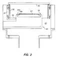
- FIG. 2A vacuum processing chamber according to another embodiment of the present invention is illustrated in FIG. 2.
- the vacuum processing chamber 40includes a substrate holder 42 providing an electrostatic clamping force to a substrate 43 as well as an RF bias to a substrate supported thereon.
- a focus ring 44having outer dielectric portion 44a and inner SiC portion 44b confines plasma in an area above the substrate while it is He backcooled.
- a source of energy for maintaining a high density (e.g. 10 11 -10 12 ions/cm 3 ) plasma in the chambersuch as an antenna (not shown) powered by a suitable RF source and suitable RF impedance matching circuitry inductively couples RF energy into the chamber 40 so as to provide a high density plasma.
- a source of energy for maintaining a high density (e.g. 10 11 -10 12 ions/cm 3 ) plasma in the chambersuch as an antenna (not shown) powered by a suitable RF source and suitable RF impedance matching circuitry inductively couples RF energy into the chamber 40 so as
- the chamberincludes suitable vacuum pumping apparatus for maintaining the interior of the chamber at a desired pressure (e.g. below 50 m Torr, typically 1-20 mTorr).
- a substantially planar dielectric window of uniform thicknesscan be provided between the antenna and the interior of the processing chamber 40 and to form the vacuum wall at the top of the processing chamber 40.
- a gas distribution platecommonly called a showerhead 50, is provided beneath the window and includes a plurality of openings such as circular holes (not shown) for delivering process gas supplied by a suitable gas supply to the processing chamber 40.
- a cylindrical liner 60 equivalent to the liner 30 in FIG.1extends from the gas distribution plate and surrounds the substrate holder 42.
- a baffle ring 70extends between the substrate holder 42 and the liner 60.
- the liner 60 and/or the baffle ring 70can be heated by a heating member 61 which can be heated by any suitable technique such as resistance heating, a heated fluid, etc. Details of the baffle ring 70 are shown in Fig. 4 wherein it can be seen that the baffle ring 70 includes small holes 72 and large holes 74 for passage of gases and by-products to a vacuum pump connected to the bottom of the chamber.
- a modified liner 62can include a cylindrical portion 64 and a conical portion 66.
- a heater 68includes resistive elements (not shown) which are used to maintain the portion 64 and/or portion 66 at a desired temperature.
- Substrates which are etched in an oxide etching processgenerally include an underlayer, an oxide layer which is to be etched, and a photoresist layer formed on top of the oxide layer.
- the oxide layermay be one of SiO 2 , BPSG, PSG, or other oxide material.
- the underlayermay be Si, TiN, silicide, or other underlying layer or substrate material.
- the etch selectivity, which is the etch rate of the layer to be etched compared to the photoresist etch rateis preferably around 4:1 or higher.
- the etch selectivity of the oxide layer compared to the underlayeris preferably greater than the oxide:photoresist etch selectively, e.g., 40:1.
- the silicon carbide chamber liner 30,60,62 and optionally the focus ring 44, the baffle ring 70 and/or gas distribution plate 22,50, also with exposed surface composed of silicon carbidereduces metal and/or particle contamination of substrates during processing such as etching of dielectric materials such as silicon dioxide (e.g., doped or undoped TEOS, BPSG, USG (undoped spin-on-glass), thermal oxide, plasma oxide, etc.) typically overlying a conductive layer such as silicon, polysilicon, silicide, titanium nitride, aluminum or a non-conductive material such as silicon nitride.
- dielectric materialssuch as silicon dioxide (e.g., doped or undoped TEOS, BPSG, USG (undoped spin-on-glass), thermal oxide, plasma oxide, etc.) typically overlying a conductive layer such as silicon, polysilicon, silicide, titanium nitride, aluminum or a non-conductive material such as silicon nitride.
- featuressuch as contact holes, vias, trenches, etc.
- substratessuch as semiconductor wafers (e.g., 25 or more consecutive wafers) while maintaining particle contamination of the wafers below acceptable levels.
- the chamber pressureis typically below 300 mTorr, preferably 1-40 mTorr
- the antennais powered at 200-5000 watts, preferably 300-2500 watts
- the RF biasis ⁇ 6000 watts, preferably 1000-2500 watts
- the He backpressureis 5-40 Torr, preferably 7-20 Torr.
- the process gascan include 10-200 sccm CHF 3 , 10-100 sccm C 2 HF 5 and/or 10-100 sccm C 2 F 6 .
- silicon carbide liner 30, 60, 62as a separate piece attachable to the reaction chamber by any suitable technique, for instance, bolting to an electrically grounded part of the chamber thereby providing grounding of the liner the liner can be replaced.
- silicon carbidecan be additionally provided as a coating on metal and/or ceramic parts of the chamber.
- the silicon carbidepreferably has a resistivity high enough to allow an RF antenna to couple RF energy into the chamber.
- the silicon carbidecan be hot pressed to obtain resistivity values on the order of about 5 x 10 4 ⁇ cm.
- SiC powdercan be doped with a suitable additive or sintered in a nitrogen atmosphere to form Si 3 N 4 in grain boundaries of the silicon carbide and thus raise the resistivity to values such as 1 x 10 8 ⁇ cm.
- suitable gas passages and outlet holescan be provided in a green ceramic material which is later sintered to form a unitary plate.
- the dimensions of the passages and holesare preferably small enough to avoid conditions under which plasma would form during flow of process gas and powering of the antenna.
- the liner and optionally the focus ring, baffle plate and/or gas distribution platecan be made of various blends of silicon carbide based powder material having a predominant amount of silicon carbide.
- the total amount of silicon and carbonis typically at least 90 wt %, preferably ⁇ 95 wt %, and more preferably ⁇ 99 wt %.
- the SiC membermay include up to about 0.5 % B to aid sintering of the SiC powder.
- the SiC membermay include an excess of Si such as up to about 35 wt % free Si and/or Si 3 N 4 .
- the silicon carbide materialcan be made by any suitable process such as hot pressing, sintering, reaction bonding (e.g., wherein SiC is infiltrated with molten Si), etc.
- the silicon carbidepreferably has a low resistivity such as below 200 ⁇ cm. The resistivity is much higher, however, when the additional SiC member is used for a window and/or gas distribution plate used in conjunction with an RF antenna. If a different RF source is used, the window/gas distribution plate can be replaced with a low resistivity SiC member.
- the SiC memberis preferably made by a process which avoids the presence of such metals in the SiC member.
- the silicon and carbonare preferably present in amounts sufficient achieve a nominal SiC stoichiometry. Such mixtures can be formed into a desired shape, sintered and machined to desired tolerances and/or surface finishes on surfaces such as vacuum sealing surfaces.
- the SiC memberpreferably is highly dense, e.g., having a density over 3.1 g/cm 3 .
- SiC memberis formed by CVD
- SiCcan be deposited on a graphite mandrel and when a desired thickness of SiC is achieved, the graphite mandrel can be etched away leaving a highly pure and highly dense SiC member.
- the silicon carbide liner and other optional members according to the inventionprovides dramatic reduction in particle count on wafers processed during oxide etching and oxygen cleaning steps.
- the silicon carbide liner and other optional membersalso reduces particle contamination during an ashing process wherein 750 sccm oxygen gas can be run for 10 seconds with the TCPTM power at 650 W, the bottom electrode at 750 W and the pressure at 10 mTorr.
- a silicon carbide linerprovides better contamination performance since there is preferably less than 200 ppm A1 in the silicon carbide material.
- by-products produced as a result of erosion of the SiCare volatile and thus do not contribute to adding particles on the wafers and the liberated elements Si and C are not detrimental to wafer processing.
Landscapes
- Physics & Mathematics (AREA)
- Engineering & Computer Science (AREA)
- Plasma & Fusion (AREA)
- Chemical & Material Sciences (AREA)
- Analytical Chemistry (AREA)
- Drying Of Semiconductors (AREA)
- Chemical Vapour Deposition (AREA)
- Arc Welding In General (AREA)
Abstract
Description
- The invention relates to improvements in a plasma processing chamber and to a method of processing a substrate in the plasma processing chamber such as by plasma etching an oxide layer on a semiconductor wafer.
- Vacuum processing chambers are generally used for chemical vapor depositing (CVD) and etching of materials on substrates by supplying process gas to the vacuum chamber and application of an RF field to the gas. Examples of parallel plate, transformer coupled plasma (TCP™, also called ICP), and electron-cyclotron resonance (ECR) reactors are disclosed in commonly owned U.S. Patent Nos. 4,340,462; 4,948,458; and 5,200,232. The substrates are held in place within the vacuum chamber during processing by substrate holders.
- Conventional substrate holders include mechanical clamps and electrostatic clamps (ESC). Examples of mechanical clamps and ESC substrate holders are provided in commonly owned U.S, Patent No. 5,262,029 and commonly owned U.S. Patent No. 5,671,116 filed on March 10, 1995. Substrate holders in the form of an electrode can supply radiofrequency (RF) power into the chamber, as disclosed in U.S. Patent No. 4,579,618. According to U.S. Patent No. 5,292,399, metal surfaces of wafer support and clamping ring mechanisms can be covered with insulating material to prevent erosion by the plasma and electrically conductive material can be used to reduce arcing due to charge build-up on such insulation surfaces.
- Plasma processing systems wherein an antenna coupled to a radio frequency (RF) Source energize gas into a plasma state within a process chamber are disclosed in US Patent No's 4,948,458; 5,198,718; 5,241,245 and 5,401,350. In such systems the antenna is located outside the process chamber and the RF energy is supplied to the chamber through a dielectric window. Such process systems can be used for a variety of semiconductor processing applications such as etching, deposition, resist stripping, etc.
- The applicant may be further enlightened as to the state of the art by reference to EP-A-0 821 397 which discloses a silicon carbide composite article particularly useful for plasma reactors and exhibiting steps and components corresponding to those recited in the precharacterising parts of
claims 1 and 12 herein. - An object of the invention is to reduce metal and/or particle contamination of plasma processed substrates when substrates are processed continuously. US-A-5,085,727 describes a method of processing a substrate and a process chamber for carrying out the method.
- Accordingly the present invention provides a method of processing a substrate according to claim 1.
- The processing chamber can include a substantially planar antenna and the process gas can be energised into the plasma state by supplying RF power to the antenna. The plasma can comprise a high density plasma and the substrates can be processed by etching an oxide layer on the substrates with the high density plasma while supplying an RF bias to the substrates.
- According to a further aspect of the present invention there is provided a plasma processing chamber according to
claim 12. - At least one further exposed surface composed of a silicon carbide based material can be provided and in this case the further surface is defined by a gas distribution plate supplying the process gas to the process chamber, a perforated baffle extending between the substrate holder and the liner and/or the focus ring surrounding the substrate. The liner the distribution plate the baffle and/or the focus ring consist essentially of hot-pressed sintered , CVD or reaction bonded SiC or a composite wherein a coating of SiC forms the exposed surface thereof The chamber can further include a dielectric window adjacent the gas distribution plate and the RF energy source or planar antenna can be adjacent the window to supply power through the window to energize the process gas in the processing chamber into a plasma state. The antenna can be arranged such that the gas outlets in the gas distribution plate are not directly between the substrate holder and the antenna. The dielectric window can have a substantially uniform thickness and substantially planar configuration and the gas distribution plate can have a substantially uniform thickness and substantially planar configuration.
- The invention will be described in greater detail with reference to the accompanying drawings in which like elements bear like reference numerals, and wherein:
- FIG. 1 is a cross sectional view of a vacuum processing chamber constructed in accordance with the invention;
- FIG. 2 is a cross sectional view of a modified vacuum processing chamber according to the invention wherein the liner is cylindrical in shape;
- FIG. 3 is a cross sectional view of a portion of a modified vacuum processing chamber in accordance with the invention wherein the liner includes a cylindrical portion and a conical portion; and
- FIG. 4 is a top view of a baffle ring usable in the processing chamber according to the invention.
- In plasma gas processing of semiconductor substrates such as silicon wafers, high density plasmas typically cause a relatively high erosion rate of chamber interior surfaces they contact due to physical and/or chemical sputtering. This is an important issue in applications for wafer processing in the semiconductor industry, due to the sensitivity of devices on the wafer to contamination from metals which are deep impurities in silicon such as nickel and iron, alkali metals such as sodium and potassium that are mobile ions in the gate oxide of devices causing unstable threshold voltage, and metals such as aluminum which cause leakage currents in device junctions resulting, for example, in short refresh times in DRAM memory cells. Because of this, the surfaces of the chamber exposed to the high density plasma in such wafer processing tools are normally covered with a nonmetallic material such as alumina or quartz.
- Alumina and quartz are dielectric materials which present a high impedance to the RF current used to sustain the plasma, and the RF current used to induce a bias voltage on the wafer. As a result, the RF current through the plasma does not have a good ground path and can become unstable, resulting in non-repeatable etch results. Moreover, charge build-up on the dielectric materials can cause arcing and thus localized sputtering of the dielectric materials.
- The present invention uses a liner acting as a side wall of the processing chamber as a separate component with a surface of silicon carbide (SiC) as a consumable chamber surface material which reduces metal and/or particle contamination of the processed substrates. The liner component is electrically conductive so that when it is in contact with the plasma it presents a good ground path for the RF current. The SiC liner provides a grounded surface which is resistant to erosion from ion bombardment and reduces plasma potential on surfaces in the chamber. The liner can consist entirely of SiC, comprise a SiC coated material such as SiC coated graphite, or principally SiC with 10 to 20% Si added to fill porosity in reaction bonded SiC. The SiC also etches at a slow rate by the plasma making the component a cost effective consumable part. Moreover, because the SiC is of high purity, wafer contamination resulting from chemical sputtering of the SiC by the plasma can be minimized. Further, the grounded SiC liner component can reduce sputtering of other surfaces in the chamber by causing a reduction in the plasma potential and hence ion bombardment energy to these non-silicon carbide surfaces. To the extent the SiC component replaces alumina as a chamber surface, aluminium contamination of wafers can be reduced. Finally, the SiC component provides a very stable plasma potential so that etch results are more repeatable within an individual chamber and from chamber to chamber.
- The invention provides improvements in reducing contamination of substrates such as semiconductor wafers, flat panel display substrates, and the like. The reduced contamination can be enhanced by utilizing silicon carbide as the material for additional members with exposed surfaces adjacent the substrate being processed in the chamber. Such additional members include non-electrically driven chamber parts such as focus rings, gas distribution plates, baffle plates and the like. The liner can provide a better RF return path for the powered electrode (bottom electrode) in the wafer support.
- In plasma etching, features can be etched into layers of various materials on substrates such as silicon wafers. In such etching processes, a gas distribution plate can be used to control the spatial distribution of gas flow in the volume of the reactor above the plane of the wafer. In the TCP 9100™ plasma etching reactor available from LAM Research Corporation, the gas distribution plate is a circular plate situated directly below the TCP™ window which is also the vacuum sealing surface at the top of the reactor in a plane above and parallel to the wafer. The gas distribution plate is sealed using an O-ring to a gas distribution ring located at the periphery of the gas distribution plate. The gas distribution ring feeds gas from a source into the volume defined by the gas distribution plate, an inside surface of a window underlying a coil supplying RF energy into the reactor, and the gas distribution ring. The gas distribution plate contains an array of holes of a specified diameter which extend through the plate. The spatial distribution of the holes through the gas distribution plate can be varied to optimize etch uniformity of the layers to be etched, e.g., a photoresist layer, a silicon dioxide layer and an underlayer material on the wafer. The cross-sectional shape of the gas distribution plate can be varied to manipulate the distribution of RF power into the plasma in the reactor. The gas distribution plate material must be a dielectric to enable coupling of this RF power through the gas distribution plate into the reactor. Further, the material of the gas distribution plate must be highly resistant to chemical sputter-etching in environments such as oxygen or a hydrofluorocarbon gas plasma in order to avoid breakdown and the resultant particle generation associated therewith. Moreover, the material of the gas distribution plate should have low levels of contaminants that might otherwise affect performance of devices on the wafer. According to a preferred embodiment of the invention, the gas distribution plate can be of specially prepared silicon carbide having high resistivity.
- It has surprisingly and unexpectedly been found that use of silicon carbide for interior chamber surfaces provides performance results which far exceed other materials such as aluminium nitride and alumina.
- A vacuum processing chamber according to one embodiment of the present invention is illustrated in FIG. 1. The
vacuum processing chamber 10 includes asubstrate holder 12 providing an electrostatic clamping force to asubstrate 13 as well as an RF bias to a substrate while it is He backcooled. Afocus ring 14 comprising a dielectricouter ring 14a and a SiCinner ring 14b confines plasma in an area above the substrate. A source of energy for maintaining a high density (e.g., 1011-1012 ions/cm3) plasma in the chamber such as anantenna 18 powered by a suitable RF source and suitable RF impedance matching circuitry inductively coupled RF energy into thechamber 10 so as to provide a high density plasma. The chamber includes suitable vacuum pumping apparatus for maintaining the interior of the chamber at a desired pressure (e.g., below 50 mTorr, typically 1-20 mTorr). A substantially planardielectric window 20 of uniform thickness provided between theantenna 18 and the interior of theprocessing chamber 10 forms the vacuum wall at the top of theprocessing chamber 10. Agas distribution plate 22 is provided beneathwindow 20 and includes openings such as circular holes for delivering process gas from thegas supply 23 to thechamber 10. In accordance with the invention, a separateconical liner 30 with an exposed surface acting as a side wall of thechamber 10 and composed of a silicon carbide based material extends from the gas distribution plate and surrounds thesubstrate holder 12. Theliner 30 is electrically grounded to provide a path for the RF energy. Theantenna 18 can be provided with achannel 24 through which a temperature control fluid is passed via inlet andoutlet conduit antenna 18 and/orwindow 20 could be cooled by other techniques such as by blowing air over the antenna and window, passing a cooling medium through or in heat transfer contact with the window and/or gas distribution plate, etc. - In operation, a wafer is positioned on the
substrate holder 12 and is typically held in place by an electrostatic clamp, a mechanical clamp, or other clamping mechanism when He backcooling is employed. Process gas is then supplied to thevacuum processing chamber 10 by passing the process gas through a gap between thewindow 20 and thegas distribution plate 22. Suitable gas distribution plate arrangements (i.e., showerhead) arrangements are disclosed in commonly owned U.S. Patent Nos. 5,824,605; 6,048,798 and 5,863,376, the disclosures of which are hereby incorporated by reference. For instance, while the window and gas distribution plate arrangement in FIG. 1 are planar and of uniform thickness, non-planar and/or non-uniform thickness geometries can be used for the window and/or gas distribution plate. A high density plasma is ignited in the space between the substrate and the window by supplying suitable RF power to theantenna 18. A temperature control fluid can also be passed through thechannel 24 in theantenna 18 to maintain theantenna 18,window 20 andgas distribution plate 22 at a temperature below a threshold temperature such as less than 120°C, preferably below 90°C and more preferably below 80°C. - A vacuum processing chamber according to another embodiment of the present invention is illustrated in FIG. 2. The
vacuum processing chamber 40 includes asubstrate holder 42 providing an electrostatic clamping force to asubstrate 43 as well as an RF bias to a substrate supported thereon. Afocus ring 44 having outerdielectric portion 44a andinner SiC portion 44b confines plasma in an area above the substrate while it is He backcooled. A source of energy for maintaining a high density (e.g. 1011-1012 ions/cm3) plasma in the chamber such as an antenna (not shown) powered by a suitable RF source and suitable RF impedance matching circuitry inductively couples RF energy into thechamber 40 so as to provide a high density plasma. The chamber includes suitable vacuum pumping apparatus for maintaining the interior of the chamber at a desired pressure (e.g. below 50 m Torr, typically 1-20 mTorr). A substantially planar dielectric window of uniform thickness can be provided between the antenna and the interior of theprocessing chamber 40 and to form the vacuum wall at the top of theprocessing chamber 40. A gas distribution plate, commonly called ashowerhead 50, is provided beneath the window and includes a plurality of openings such as circular holes (not shown) for delivering process gas supplied by a suitable gas supply to theprocessing chamber 40. Acylindrical liner 60 equivalent to theliner 30 in FIG.1 extends from the gas distribution plate and surrounds thesubstrate holder 42. Abaffle ring 70 extends between thesubstrate holder 42 and theliner 60. Theliner 60 and/or thebaffle ring 70 can be heated by aheating member 61 which can be heated by any suitable technique such as resistance heating, a heated fluid, etc. Details of thebaffle ring 70 are shown in Fig. 4 wherein it can be seen that thebaffle ring 70 includessmall holes 72 andlarge holes 74 for passage of gases and by-products to a vacuum pump connected to the bottom of the chamber. - In another embodiment, as shown in Fig. 3, a modified liner 62 can include a
cylindrical portion 64 and aconical portion 66. In this embodiment, aheater 68 includes resistive elements (not shown) which are used to maintain theportion 64 and/orportion 66 at a desired temperature. - Substrates which are etched in an oxide etching process generally include an underlayer, an oxide layer which is to be etched, and a photoresist layer formed on top of the oxide layer. The oxide layer may be one of SiO2, BPSG, PSG, or other oxide material. The underlayer may be Si, TiN, silicide, or other underlying layer or substrate material. The etch selectivity, which is the etch rate of the layer to be etched compared to the photoresist etch rate is preferably around 4:1 or higher. The etch selectivity of the oxide layer compared to the underlayer is preferably greater than the oxide:photoresist etch selectively, e.g., 40:1.
- According to the invention, the silicon
carbide chamber liner focus ring 44, thebaffle ring 70 and/orgas distribution plate - During oxide etching, the chamber pressure is typically below 300 mTorr, preferably 1-40 mTorr, the antenna is powered at 200-5000 watts, preferably 300-2500 watts, the RF bias is ≤ 6000 watts, preferably 1000-2500 watts, and the He backpressure is 5-40 Torr, preferably 7-20 Torr. The process gas can include 10-200 sccm CHF3, 10-100 sccm C2HF5 and/or 10-100 sccm C2F6.
- By making the
silicon carbide liner - Principally the liner and optionally the focus ring, baffle plate and/or gas distribution plate can be made of various blends of silicon carbide based powder material having a predominant amount of silicon carbide. For instance, the total amount of silicon and carbon is typically at least 90 wt %, preferably ≥ 95 wt %, and more preferably ≥ 99 wt %. For example, the SiC member may include up to about 0.5 % B to aid sintering of the SiC powder. The SiC member may include an excess of Si such as up to about 35 wt % free Si and/or Si3N4. The silicon carbide material can be made by any suitable process such as hot pressing, sintering, reaction bonding (e.g., wherein SiC is infiltrated with molten Si), etc. For the liner and optionally the focus ring and/or baffle, the silicon carbide preferably has a low resistivity such as below 200 Ω·cm. The resistivity is much higher, however, when the additional SiC member is used for a window and/or gas distribution plate used in conjunction with an RF antenna. If a different RF source is used, the window/gas distribution plate can be replaced with a low resistivity SiC member. In order to avoid metal contamination during processing of semiconductor substrates, the SiC member is preferably made by a process which avoids the presence of such metals in the SiC member. The silicon and carbon are preferably present in amounts sufficient achieve a nominal SiC stoichiometry. Such mixtures can be formed into a desired shape, sintered and machined to desired tolerances and/or surface finishes on surfaces such as vacuum sealing surfaces. The SiC member preferably is highly dense, e.g., having a density over 3.1 g/cm3.
- In the case where the SiC member is formed by CVD, it is preferable to deposit enough SiC to form a bulk member. For instance, SiC can be deposited on a graphite mandrel and when a desired thickness of SiC is achieved, the graphite mandrel can be etched away leaving a highly pure and highly dense SiC member.
- The silicon carbide liner and other optional members according to the invention provides dramatic reduction in particle count on wafers processed during oxide etching and oxygen cleaning steps. The silicon carbide liner and other optional members also reduces particle contamination during an ashing process wherein 750 sccm oxygen gas can be run for 10 seconds with the TCP™ power at 650 W, the bottom electrode at 750 W and the pressure at 10 mTorr. Compared to an alumina liner which is attacked during the etching and oxygen cleaning steps and can liberate aluminum which could contaminate wafers, a silicon carbide liner provides better contamination performance since there is preferably less than 200 ppm A1 in the silicon carbide material. Moreover, during processing such as plasma etching, by-products produced as a result of erosion of the SiC are volatile and thus do not contribute to adding particles on the wafers and the liberated elements Si and C are not detrimental to wafer processing.
- The foregoing has described the principles, preferred embodiments and modes of operation of the present invention. However, the invention should not be construed as being limited to the particular embodiments discussed. Thus, the above-described embodiments should be regarded as illustrative rather than restrictive, and it should be appreciated that variations may be made in those embodiments by workers skilled in the art without departing from the scope of the present invention as defined by ,the following claims.
Claims (21)
- A method of processing a substrate (13, 43) comprising the steps of:(a) placing a substrate (13, 43) on a substrate holder (12, 42) in a processing chamber (10, 40), the processing chamber (10, 40) having at least one exposed surface adjacent the substrate (13, 43) composed of a silicon carbide based material;(b) processing the substrate (13, 43) by supplying process gas to the processing chamber and energizing the process gas into a plasma state in the processing chamber by the supply of RF energy, the exposed surface being exposed to the plasma;(c) removing the substrate (13, 43) from the processing chamber; and(d) consecutively processing additional substrates in the processing chamber by repeating steps (a-c) while minimizing particle contamination of the substrates during the processing step as a result of reduction of plasma potential on the silicon carbide surface and/or reduced sputtering of non-silicon carbide chamber interior surfaces; the exposed surface is defined by a liner (30,60,62) of the processing chamber,characterised by:using a liner (30,60,62) formed entirely of CVD SiC to provide a highly uniform temperature distribution across the exposed surface area thereof during the processing step,and by electrically grounding the liner (30,60,62) to provide a return path for RF during the processing stepand byheating the liner (30,60,62) by means of a heater.
- The method according to claim 1 wherein liner (30,60,62) piece is attached by bolting.
- The method according to claim 1 or 2, wherein the processing chamber includes a substantially planar antenna (18) which energizes the process gas into the plasma state by supplying RF power to the antenna and the process gas comprising one or more hydrofluorocarbon gases.
- The method according to claim 1, wherein the plasma comprises a high density plasma and the substrates are processed by etching an oxide layer on the substrates with the high density plasma while supplying an RF bias to the substrates.
- The method according to any one of the preceding claims, wherein there is at least one further exposed surface composed of a silicon carbide based material and the further exposed surface is defined by a gas distribution plate (22, 50) supplying the process gas to the processing chamber, a perforated baffle (70) extending between the substrate holder and the liner (30,60,62) and/or a focus ring (14, 14b, 44, 44b) surrounding the substrate (13, 43).
- The method according to any one of claims 1 to 4, wherein the liner (30,60,62) is heated to a temperature above room temperature during the processing step and a baffle (70) extends between the substrate holder and the liner (30,60,62), the liner (30,60,62) surrounding the substrate holder and the baffle comprising a foraminous ring.
- The method according to claim 6, wherein the baffle (70) also has an exposed surface composed of a silicon carbide based material.
- The method according to any one of claims 1 to 4, wherein the process gas is supplied by a gas distribution plate (22, 50) also having an exposed surface composed of a silicon carbide based material and having a resistivity high enough to make the silicon carbide an insulating material.
- The method according to any one of claims 1 to 8, wherein the heated member surrounds the liner (30, 60, 62) to maintain the liner (30, 60, 62) at a desired temperature.
- The method according to any one of claims 1 to 9, wherein the liner (30,60,62), the distribution plate, the baffle and/or the focus ring consists essentially of hot-pressed, sintered, CVD or reaction bonded SiC or a composite wherein a coating of SiC forms the exposed surface thereof.
- The method according to any one of claims 1 to 10, wherein the liner (30,60,62) has a resistivity below 200 Ω·cm.
- A plasma processing chamber comprising:a substrate holder (12, 42) for supporting a substrate (13, 43) within an interior of the processing chamber;an exposed surface adjacent the substrate (13, 43) composed of silicon carbide based material;a gas supply (23) for supplying process gas to the interior of the processing chamber; andan energy source (18) supplying RF energy into the interior of the processing chamber and energizing the process gas into a plasma state for processing a substrate (13, 43), the silicon carbide surface minimizing particle contamination of substrates during plasma processing thereof as a result of reduction of plasma potential on the silicon carbide surface and/or reduced sputtering of non-silicon carbide chamber interior surfaces; wherein the exposed surface is defined by a liner (30,60,62)characterized in that the liner (30,60,62)
is formed entirely of CVD SiC to provide a highly uniform temperature distribution across the exposed surface thereof during the process,
the liner (30,60,62) is electrically grounded to provide a return path for the RF during the processing step and
a heater (68) is provided to heat the liner (30,60,62). - A plasma processing chamber according to claim 12 wherein the liner (30,60,62) piece is attached by bolts.
- The plasma processing chamber according to one of claims 12 or 13, wherein the heater (68)is provided by a heated member which surrounds the liner (30,60,62) and maintains the liner (30,60,62) at the desired temperature.
- The plasma processing chamber according to one of claims 12 to 14, wherein the processing chamber includes a dielectric window (20) and the energy source comprises a substantially planar antenna (18) adjacent the window, the antenna supplying RF power through the window to energize process gas in the processing chamber into a plasma state.
- The plasma processing chamber according to one of claims 12 to 15, wherein at least one further exposed surface composed of a silicon carbide based material is provided, the further exposed surface being defined by a gas distribution plate (22, 50) supplying the process gas, a focus ring (14, 14b, 44, 44b) surrounding the substrate holder and/or a perforated baffle (70) between the substrate holder and the liner (30,60,62).
- The plasma processing chamber according to claim 16, wherein the component with the further exposed surface has a resistivity of at least 5 x 10⁴ Ω·cm.
- The plasma processing chamber according to any one of claims 12 to 17, wherein the liner (30,60,62) is composed of a cylindrical and/or conical portions.
- The plasma processing chamber according to claim 16, wherein the further exposed surface is defined by the distribution plate which has a resistivity high enough to make the gas distribution plate an insulating material and the liner (30,60,62) having a resistivity low enough to make the liner (30,60,62) electrically conducting.
- The plasma processing chamber according to any one of claims 12 to 19, wherein the liner (30,60,62), the distribution plate, the focus ring and/or the baffle consists essentially of hot-pressed, sintered, CVD or reaction bonded SiC or a composite, wherein a coating of SiC forms the exposed surface thereof.
- The plasma processing chamber according to any one of claims 12 to 20, wherein the liner (30,60,62), the distribution plate, the focus ring and/or the baffle has a density of at least 3.1 g/cm3 and includes at least 99 wt% carbon and silicon.
Applications Claiming Priority (3)
| Application Number | Priority Date | Filing Date | Title |
|---|---|---|---|
| US5090298A | 1998-03-31 | 1998-03-31 | |
| PCT/US1999/006658WO1999050886A1 (en) | 1998-03-31 | 1999-03-26 | Contamination controlling method and plasma processing chamber |
| US50902 | 2002-01-18 |
Publications (2)
| Publication Number | Publication Date |
|---|---|
| EP1068632A1 EP1068632A1 (en) | 2001-01-17 |
| EP1068632B1true EP1068632B1 (en) | 2006-11-15 |
Family
ID=21968184
Family Applications (1)
| Application Number | Title | Priority Date | Filing Date |
|---|---|---|---|
| EP99915049AExpired - LifetimeEP1068632B1 (en) | 1998-03-31 | 1999-03-26 | Contamination controlling method and plasma processing chamber |
Country Status (7)
| Country | Link |
|---|---|
| EP (1) | EP1068632B1 (en) |
| JP (1) | JP4554815B2 (en) |
| KR (1) | KR100602072B1 (en) |
| AT (1) | ATE345577T1 (en) |
| DE (1) | DE69934000T2 (en) |
| TW (1) | TW575676B (en) |
| WO (1) | WO1999050886A1 (en) |
Families Citing this family (30)
| Publication number | Priority date | Publication date | Assignee | Title |
|---|---|---|---|---|
| US6129808A (en) | 1998-03-31 | 2000-10-10 | Lam Research Corporation | Low contamination high density plasma etch chambers and methods for making the same |
| CN1251293C (en)* | 1999-11-15 | 2006-04-12 | 兰姆研究有限公司 | Materials and gas chemistries for processing systems |
| US6673198B1 (en) | 1999-12-22 | 2004-01-06 | Lam Research Corporation | Semiconductor processing equipment having improved process drift control |
| JP2001203188A (en)* | 2000-01-19 | 2001-07-27 | Ibiden Co Ltd | Component for semiconductor manufacturing machine and the machine |
| JP2001203190A (en)* | 2000-01-20 | 2001-07-27 | Ibiden Co Ltd | Component for semiconductor manufacturing machine and the machine |
| US6890861B1 (en)* | 2000-06-30 | 2005-05-10 | Lam Research Corporation | Semiconductor processing equipment having improved particle performance |
| US6506254B1 (en) | 2000-06-30 | 2003-01-14 | Lam Research Corporation | Semiconductor processing equipment having improved particle performance |
| US7166166B2 (en) | 2002-09-30 | 2007-01-23 | Tokyo Electron Limited | Method and apparatus for an improved baffle plate in a plasma processing system |
| US7204912B2 (en) | 2002-09-30 | 2007-04-17 | Tokyo Electron Limited | Method and apparatus for an improved bellows shield in a plasma processing system |
| US7137353B2 (en) | 2002-09-30 | 2006-11-21 | Tokyo Electron Limited | Method and apparatus for an improved deposition shield in a plasma processing system |
| US7147749B2 (en) | 2002-09-30 | 2006-12-12 | Tokyo Electron Limited | Method and apparatus for an improved upper electrode plate with deposition shield in a plasma processing system |
| US6837966B2 (en) | 2002-09-30 | 2005-01-04 | Tokyo Electron Limeted | Method and apparatus for an improved baffle plate in a plasma processing system |
| US7166200B2 (en) | 2002-09-30 | 2007-01-23 | Tokyo Electron Limited | Method and apparatus for an improved upper electrode plate in a plasma processing system |
| US6798519B2 (en) | 2002-09-30 | 2004-09-28 | Tokyo Electron Limited | Method and apparatus for an improved optical window deposition shield in a plasma processing system |
| US7780786B2 (en) | 2002-11-28 | 2010-08-24 | Tokyo Electron Limited | Internal member of a plasma processing vessel |
| KR101016913B1 (en) | 2003-03-31 | 2011-02-22 | 도쿄엘렉트론가부시키가이샤 | Barrier layer for processing element and method of forming the same |
| JP4597972B2 (en) | 2003-03-31 | 2010-12-15 | 東京エレクトロン株式会社 | A method of bonding adjacent coatings on a processing member. |
| US7552521B2 (en) | 2004-12-08 | 2009-06-30 | Tokyo Electron Limited | Method and apparatus for improved baffle plate |
| US7700494B2 (en) | 2004-12-30 | 2010-04-20 | Tokyo Electron Limited, Inc. | Low-pressure removal of photoresist and etch residue |
| US7601242B2 (en) | 2005-01-11 | 2009-10-13 | Tokyo Electron Limited | Plasma processing system and baffle assembly for use in plasma processing system |
| KR100719804B1 (en)* | 2005-08-08 | 2007-05-18 | 주식회사 아이피에스 | Multi-antenna structure |
| KR100694796B1 (en)* | 2005-09-26 | 2007-03-14 | 세메스 주식회사 | Gas-liquid Separator in Flat-Panel Display Chamber |
| KR100855323B1 (en)* | 2006-12-27 | 2008-09-04 | 세메스 주식회사 | Process chamber and plasma processing unit |
| US20090151870A1 (en)* | 2007-12-14 | 2009-06-18 | Tokyo Electron Limited | Silicon carbide focus ring for plasma etching system |
| KR101398585B1 (en)* | 2012-10-08 | 2014-06-27 | 주식회사 코디에스 | Plasma etching apparatus and baffle |
| US10074887B2 (en) | 2016-06-29 | 2018-09-11 | Google Llc | Antenna chamber with heat venting |
| US10418223B1 (en)* | 2018-03-30 | 2019-09-17 | Varian Semiconductor Equipment Associates, Inc. | Foil sheet assemblies for ion implantation |
| US11239060B2 (en) | 2018-05-29 | 2022-02-01 | Taiwan Semiconductor Manufacturing Company, Ltd. | Ion beam etching chamber with etching by-product redistributor |
| JP7182916B2 (en)* | 2018-06-26 | 2022-12-05 | 東京エレクトロン株式会社 | Plasma processing equipment |
| US11776793B2 (en)* | 2020-11-13 | 2023-10-03 | Applied Materials, Inc. | Plasma source with ceramic electrode plate |
Citations (5)
| Publication number | Priority date | Publication date | Assignee | Title |
|---|---|---|---|---|
| US5085727A (en)* | 1990-05-21 | 1992-02-04 | Applied Materials, Inc. | Plasma etch apparatus with conductive coating on inner metal surfaces of chamber to provide protection from chemical corrosion |
| US5182059A (en)* | 1989-01-17 | 1993-01-26 | Ngk Insulators, Ltd. | Process for producing high density SiC sintered bodies |
| US5292399A (en)* | 1990-04-19 | 1994-03-08 | Applied Materials, Inc. | Plasma etching apparatus with conductive means for inhibiting arcing |
| US5441568A (en)* | 1994-07-15 | 1995-08-15 | Applied Materials, Inc. | Exhaust baffle for uniform gas flow pattern |
| US5556501A (en)* | 1989-10-03 | 1996-09-17 | Applied Materials, Inc. | Silicon scavenger in an inductively coupled RF plasma reactor |
Family Cites Families (10)
| Publication number | Priority date | Publication date | Assignee | Title |
|---|---|---|---|---|
| JPH0741153Y2 (en)* | 1987-10-26 | 1995-09-20 | 東京応化工業株式会社 | Sample processing electrode |
| GB8905073D0 (en)* | 1989-03-06 | 1989-04-19 | Nordiko Ltd | Ion gun |
| JPH0464883A (en)* | 1990-07-04 | 1992-02-28 | Mitsubishi Electric Corp | Defrosting device for freezing and/or refrigerating chamber |
| US5304279A (en)* | 1990-08-10 | 1994-04-19 | International Business Machines Corporation | Radio frequency induction/multipole plasma processing tool |
| US6036877A (en)* | 1991-06-27 | 2000-03-14 | Applied Materials, Inc. | Plasma reactor with heated source of a polymer-hardening precursor material |
| JPH08115903A (en)* | 1994-10-14 | 1996-05-07 | Fujitsu Ltd | Method for manufacturing semiconductor device and plasma etching apparatus |
| EP0756309A1 (en)* | 1995-07-26 | 1997-01-29 | Applied Materials, Inc. | Plasma systems for processing substrates |
| US6156663A (en)* | 1995-10-03 | 2000-12-05 | Hitachi, Ltd. | Method and apparatus for plasma processing |
| US5904778A (en)* | 1996-07-26 | 1999-05-18 | Applied Materials, Inc. | Silicon carbide composite article particularly useful for plasma reactors |
| US5942454A (en)* | 1996-08-27 | 1999-08-24 | Asahi Glass Company Ltd. | Highly corrosion-resistant silicon carbide product |
- 1999
- 1999-03-26KRKR1020007010806Apatent/KR100602072B1/ennot_activeExpired - Fee Related
- 1999-03-26DEDE69934000Tpatent/DE69934000T2/ennot_activeExpired - Lifetime
- 1999-03-26JPJP2000541718Apatent/JP4554815B2/ennot_activeExpired - Fee Related
- 1999-03-26WOPCT/US1999/006658patent/WO1999050886A1/enactiveIP Right Grant
- 1999-03-26EPEP99915049Apatent/EP1068632B1/ennot_activeExpired - Lifetime
- 1999-03-26ATAT99915049Tpatent/ATE345577T1/ennot_activeIP Right Cessation
- 1999-03-31TWTW88105064Apatent/TW575676B/ennot_activeIP Right Cessation
Patent Citations (5)
| Publication number | Priority date | Publication date | Assignee | Title |
|---|---|---|---|---|
| US5182059A (en)* | 1989-01-17 | 1993-01-26 | Ngk Insulators, Ltd. | Process for producing high density SiC sintered bodies |
| US5556501A (en)* | 1989-10-03 | 1996-09-17 | Applied Materials, Inc. | Silicon scavenger in an inductively coupled RF plasma reactor |
| US5292399A (en)* | 1990-04-19 | 1994-03-08 | Applied Materials, Inc. | Plasma etching apparatus with conductive means for inhibiting arcing |
| US5085727A (en)* | 1990-05-21 | 1992-02-04 | Applied Materials, Inc. | Plasma etch apparatus with conductive coating on inner metal surfaces of chamber to provide protection from chemical corrosion |
| US5441568A (en)* | 1994-07-15 | 1995-08-15 | Applied Materials, Inc. | Exhaust baffle for uniform gas flow pattern |
Also Published As
| Publication number | Publication date |
|---|---|
| JP2002510858A (en) | 2002-04-09 |
| KR100602072B1 (en) | 2006-07-14 |
| JP4554815B2 (en) | 2010-09-29 |
| EP1068632A1 (en) | 2001-01-17 |
| DE69934000D1 (en) | 2006-12-28 |
| DE69934000T2 (en) | 2007-09-20 |
| ATE345577T1 (en) | 2006-12-15 |
| TW575676B (en) | 2004-02-11 |
| KR20010042268A (en) | 2001-05-25 |
| WO1999050886A1 (en) | 1999-10-07 |
Similar Documents
| Publication | Publication Date | Title |
|---|---|---|
| EP1068632B1 (en) | Contamination controlling method and plasma processing chamber | |
| US6464843B1 (en) | Contamination controlling method and apparatus for a plasma processing chamber | |
| US5993594A (en) | Particle controlling method and apparatus for a plasma processing chamber | |
| US6033585A (en) | Method and apparatus for preventing lightup of gas distribution holes | |
| EP1145273B1 (en) | Low contamination high density plasma etch chambers and methods for making the same | |
| US6451157B1 (en) | Gas distribution apparatus for semiconductor processing | |
| KR101432832B1 (en) | An edge ring assembly having a dielectric spacer ring | |
| US7132618B2 (en) | MERIE plasma reactor with overhead RF electrode tuned to the plasma with arcing suppression | |
| EP1346076B1 (en) | Low contamination plasma chamber components and methods for making the same | |
| US7524397B2 (en) | Lower electrode design for higher uniformity | |
| US5812362A (en) | Method and apparatus for the use of diamond films as dielectric coatings on electrostatic chucks | |
| JPH10189296A (en) | Parallel plate electrode plasma reactor | |
| WO2008134446A1 (en) | Annular baffle |
Legal Events
| Date | Code | Title | Description |
|---|---|---|---|
| PUAI | Public reference made under article 153(3) epc to a published international application that has entered the european phase | Free format text:ORIGINAL CODE: 0009012 | |
| 17P | Request for examination filed | Effective date:20000918 | |
| AK | Designated contracting states | Kind code of ref document:A1 Designated state(s):AT CH DE FI FR GB IE IT LI NL SE | |
| 17Q | First examination report despatched | Effective date:20011119 | |
| GRAP | Despatch of communication of intention to grant a patent | Free format text:ORIGINAL CODE: EPIDOSNIGR1 | |
| GRAS | Grant fee paid | Free format text:ORIGINAL CODE: EPIDOSNIGR3 | |
| GRAA | (expected) grant | Free format text:ORIGINAL CODE: 0009210 | |
| AK | Designated contracting states | Kind code of ref document:B1 Designated state(s):AT CH DE FI FR GB IE IT LI NL SE | |
| PG25 | Lapsed in a contracting state [announced via postgrant information from national office to epo] | Ref country code:NL Free format text:LAPSE BECAUSE OF FAILURE TO SUBMIT A TRANSLATION OF THE DESCRIPTION OR TO PAY THE FEE WITHIN THE PRESCRIBED TIME-LIMIT Effective date:20061115 Ref country code:LI Free format text:LAPSE BECAUSE OF FAILURE TO SUBMIT A TRANSLATION OF THE DESCRIPTION OR TO PAY THE FEE WITHIN THE PRESCRIBED TIME-LIMIT Effective date:20061115 Ref country code:IT Free format text:LAPSE BECAUSE OF FAILURE TO SUBMIT A TRANSLATION OF THE DESCRIPTION OR TO PAY THE FEE WITHIN THE PRESCRIBED TIME-LIMIT;WARNING: LAPSES OF ITALIAN PATENTS WITH EFFECTIVE DATE BEFORE 2007 MAY HAVE OCCURRED AT ANY TIME BEFORE 2007. THE CORRECT EFFECTIVE DATE MAY BE DIFFERENT FROM THE ONE RECORDED. Effective date:20061115 Ref country code:FI Free format text:LAPSE BECAUSE OF FAILURE TO SUBMIT A TRANSLATION OF THE DESCRIPTION OR TO PAY THE FEE WITHIN THE PRESCRIBED TIME-LIMIT Effective date:20061115 Ref country code:CH Free format text:LAPSE BECAUSE OF FAILURE TO SUBMIT A TRANSLATION OF THE DESCRIPTION OR TO PAY THE FEE WITHIN THE PRESCRIBED TIME-LIMIT Effective date:20061115 Ref country code:AT Free format text:LAPSE BECAUSE OF FAILURE TO SUBMIT A TRANSLATION OF THE DESCRIPTION OR TO PAY THE FEE WITHIN THE PRESCRIBED TIME-LIMIT Effective date:20061115 | |
| REG | Reference to a national code | Ref country code:GB Ref legal event code:FG4D | |
| REG | Reference to a national code | Ref country code:CH Ref legal event code:EP | |
| REF | Corresponds to: | Ref document number:69934000 Country of ref document:DE Date of ref document:20061228 Kind code of ref document:P | |
| REG | Reference to a national code | Ref country code:IE Ref legal event code:FG4D | |
| PG25 | Lapsed in a contracting state [announced via postgrant information from national office to epo] | Ref country code:SE Free format text:LAPSE BECAUSE OF FAILURE TO SUBMIT A TRANSLATION OF THE DESCRIPTION OR TO PAY THE FEE WITHIN THE PRESCRIBED TIME-LIMIT Effective date:20070215 | |
| NLV1 | Nl: lapsed or annulled due to failure to fulfill the requirements of art. 29p and 29m of the patents act | ||
| ET | Fr: translation filed | ||
| REG | Reference to a national code | Ref country code:CH Ref legal event code:PL | |
| PLBE | No opposition filed within time limit | Free format text:ORIGINAL CODE: 0009261 | |
| STAA | Information on the status of an ep patent application or granted ep patent | Free format text:STATUS: NO OPPOSITION FILED WITHIN TIME LIMIT | |
| 26N | No opposition filed | Effective date:20070817 | |
| GBPC | Gb: european patent ceased through non-payment of renewal fee | Effective date:20070326 | |
| PG25 | Lapsed in a contracting state [announced via postgrant information from national office to epo] | Ref country code:GB Free format text:LAPSE BECAUSE OF NON-PAYMENT OF DUE FEES Effective date:20070326 | |
| PGFP | Annual fee paid to national office [announced via postgrant information from national office to epo] | Ref country code:IE Payment date:20130325 Year of fee payment:15 | |
| REG | Reference to a national code | Ref country code:IE Ref legal event code:MM4A | |
| PG25 | Lapsed in a contracting state [announced via postgrant information from national office to epo] | Ref country code:IE Free format text:LAPSE BECAUSE OF NON-PAYMENT OF DUE FEES Effective date:20140326 | |
| REG | Reference to a national code | Ref country code:FR Ref legal event code:PLFP Year of fee payment:17 | |
| REG | Reference to a national code | Ref country code:FR Ref legal event code:PLFP Year of fee payment:18 | |
| PGFP | Annual fee paid to national office [announced via postgrant information from national office to epo] | Ref country code:FR Payment date:20160328 Year of fee payment:18 | |
| PGFP | Annual fee paid to national office [announced via postgrant information from national office to epo] | Ref country code:DE Payment date:20160331 Year of fee payment:18 | |
| REG | Reference to a national code | Ref country code:DE Ref legal event code:R119 Ref document number:69934000 Country of ref document:DE | |
| REG | Reference to a national code | Ref country code:FR Ref legal event code:ST Effective date:20171130 | |
| PG25 | Lapsed in a contracting state [announced via postgrant information from national office to epo] | Ref country code:FR Free format text:LAPSE BECAUSE OF NON-PAYMENT OF DUE FEES Effective date:20170331 Ref country code:DE Free format text:LAPSE BECAUSE OF NON-PAYMENT OF DUE FEES Effective date:20171003 |