EP1046939B1 - Method and apparatus for recording a flat field image - Google Patents
Method and apparatus for recording a flat field imageDownload PDFInfo
- Publication number
- EP1046939B1 EP1046939B1EP00303162AEP00303162AEP1046939B1EP 1046939 B1EP1046939 B1EP 1046939B1EP 00303162 AEP00303162 AEP 00303162AEP 00303162 AEP00303162 AEP 00303162AEP 1046939 B1EP1046939 B1EP 1046939B1
- Authority
- EP
- European Patent Office
- Prior art keywords
- lens
- image
- range
- scan
- recording medium
- Prior art date
- Legal status (The legal status is an assumption and is not a legal conclusion. Google has not performed a legal analysis and makes no representation as to the accuracy of the status listed.)
- Expired - Lifetime
Links
- 238000000034methodMethods0.000titledescription2
- 239000006185dispersionSubstances0.000claimsdescription9
- 230000003595spectral effectEffects0.000claimsdescription4
- 230000004044responseEffects0.000claimsdescription2
- 239000000463materialSubstances0.000description14
- 230000003287optical effectEffects0.000description14
- 230000004075alterationEffects0.000description10
- 238000003384imaging methodMethods0.000description6
- 239000004065semiconductorSubstances0.000description6
- CPBQJMYROZQQJC-UHFFFAOYSA-Nhelium neonChemical compound[He].[Ne]CPBQJMYROZQQJC-UHFFFAOYSA-N0.000description3
- 238000005286illuminationMethods0.000description2
- 230000009471actionEffects0.000description1
- 201000009310astigmatismDiseases0.000description1
- 230000008859changeEffects0.000description1
- 230000001419dependent effectEffects0.000description1
- 238000012986modificationMethods0.000description1
- 230000004048modificationEffects0.000description1
- 238000010408sweepingMethods0.000description1
Images


Classifications
- G—PHYSICS
- G02—OPTICS
- G02B—OPTICAL ELEMENTS, SYSTEMS OR APPARATUS
- G02B26/00—Optical devices or arrangements for the control of light using movable or deformable optical elements
- G02B26/08—Optical devices or arrangements for the control of light using movable or deformable optical elements for controlling the direction of light
- G02B26/10—Scanning systems
- G02B26/12—Scanning systems using multifaceted mirrors
- G02B26/125—Details of the optical system between the polygonal mirror and the image plane
- G—PHYSICS
- G02—OPTICS
- G02B—OPTICAL ELEMENTS, SYSTEMS OR APPARATUS
- G02B13/00—Optical objectives specially designed for the purposes specified below
- G02B13/0005—Optical objectives specially designed for the purposes specified below having F-Theta characteristic
- G—PHYSICS
- G02—OPTICS
- G02B—OPTICAL ELEMENTS, SYSTEMS OR APPARATUS
- G02B27/00—Optical systems or apparatus not provided for by any of the groups G02B1/00 - G02B26/00, G02B30/00
- G02B27/0025—Optical systems or apparatus not provided for by any of the groups G02B1/00 - G02B26/00, G02B30/00 for optical correction, e.g. distorsion, aberration
- G02B27/0031—Optical systems or apparatus not provided for by any of the groups G02B1/00 - G02B26/00, G02B30/00 for optical correction, e.g. distorsion, aberration for scanning purposes
Definitions
- This inventionrelates to an apparatus for recording or reproducing a flat field image, and in particular, to an apparatus that provides a high-quality and high-resolution image substantially insensitive to variation in illumination wavelength over a broad wavelength range.
- Some image printersuse lasers, such as helium-neon lasers or semiconductor laser diodes to generate an image modulated light beam for recording or reproducing an image or text either by exposing a photosensitive material (e.g., a film, plate, or paper) or by photosensitive charging of an electrostatic recording device.
- laserssuch as helium-neon lasers or semiconductor laser diodes to generate an image modulated light beam for recording or reproducing an image or text either by exposing a photosensitive material (e.g., a film, plate, or paper) or by photosensitive charging of an electrostatic recording device.
- semiconductor laser diodesare small, cost efficient, operate in the milliwatt range and can be readily modulated at rates up to 5 GHz by modulating its driving current, which is desirable for high resolution printing.
- helium-neon lasersare relatively large, costly, and typical require expensive optical components to provide high-resolution printing.
- semiconductor laser diodesare preferred as the source of a modulated light beam for recording in high
- chromatic aberrationscause different wavelengths of the light beam to focus at different points.
- semiconductor laser diodesproduce predominantly monochromatic light beams, they can suffer from chromatic aberrations because of power output fluctuations and multiple longitudinal mode operation that change their output wavelengths. In such cases, the chromatic aberration can produce unwanted image variations at the photosensitive material.
- EP-A-0341518US-A-5270851
- EP-A-0806691Known related systems are disclosed in EP-A-0341518, US-A-5270851 and EP-A-0806691.
- the inventionfeatures a flat field image printing apparatus.
- the printing apparatusincludes:
- Embodiments of the lens assemblycan have any of the following features.
- the lens assemblycan be configured to produce an achromatic focused beam spot in the visible and near infrared spectral wavelength range, e.g., the wavelength range of 670 nm to 780 nm.
- the range of scan anglescan be -32° to +32°.
- the first lenscan have a refractive index in the range of 1.64 to 1.85
- the second lenscan have a refractive index in the range of 1.60 to 1.75
- the third lenscan have a refractive index in the range of 1.65 to 1.75.
- the total optical power ⁇ of a multi-component systemis the reciprocal of its effective focal length at the primary design wavelength.
- the optical power ⁇ n of the n th element of the multi component systemequals the reciprocal of the focal length of the n th element at the primary design wavelength, divided by the total optical power ⁇ of the multi-component system.
- the Abbe dispersion number ⁇ n for the n th element of a multi component systemis the Abbe dispersion number ⁇ d for the material of the n th element.
- a new laser diodecan replace an old laser diode in a printing apparatus without any optical realignment, even though the wavelength produced by the new laser diode may differ from that of the old diode by as much as 20 nm.
- laser diodeshave a lifetime of about 50,000 hours and need to be replaced every 5 years. Absent the achromatic property of the lens assembly, the printing apparatus would need to be refocused and realigned by a trained operator every time a laser diode is replaced.
- the achromatic lens assemblycompensates for wavelength-dependent variations in focal size and position so that such refocusing and realignment is not necessary.
- the achromatic lens assemblycorrects for chromatic aberrations caused by the broadening of the laser line width. Such broadening can occur at low drive currents because the laser diode operates near its lasing threshold where the intensity of the laser line is low and the spectral line width is broad.
- the achromatic lens assemblycorrects for chromatic aberrations caused by the laser diode shifting to higher wavelengths. Such shifting can occur at high drive currents where the laser diode output is large. Additional chromatic aberrations compensated by the achromatic lens assembly include those caused by output power fluctuations in the laser diode caused by internal temperature variations and mode-hopping instabilities.
- the achromatic lens assemblycan also be used in high-speed printing systems that use multiple laser diodes to increase printing speed. Because the achromatic lens assembly compensates for chromatic aberrations, it is not necessary to match the wavelengths produced by the multiple laser diodes. In particular, the lens assembly allows multiple laser diodes in the same printing apparatus even though the laser diodes may have lot-to-lot variations in emission wavelength of several nanometers.
- the achromatic lens assemblyenables the printing system to expose photosensitive imaging media at different wavelengths without realigning and refocusing the system.
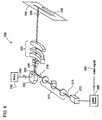
- FIG. 1schematically illustrates one embodiment of a flat field image recording apparatus 100.
- This flat field image recording apparatusprovides a two-dimensional image on photosensitive material from an electrical signal, such as an externally applied video signal 90 of this image.
- Video signal 90modulates a power source 95, which drives a light source 110.
- Light source 110converts the externally applied video signal into an image modulated visible or infrared light output that is collimated by lens 112 to form an image modulated beam 115.
- the image modulated light beam 115is deflected by a 45 degree rotatable mirror 120 towards a focusing lens system 125, which focuses the deflected light beam 145 into an image point on photosensitive material 132.
- a high-speed motor 142drives rotatable mirror 120 about a rotation axis 140.
- the beam passing through scan lens 125causes a focused spot to move in a raster-like fashion along an imaging line 135 on material 132.
- the scan angles ⁇ that are swept out during imaging by the mirror facet 150span a range from approximately -32° to +32°.
- information contained in the deflected light beam 130exposes photosensitive material 132 in a sweep or scan-like manner.
- motor 140rotates the mirror 120 at a pre-determined angular velocity.
- the strip 135is a very fine, for example, less than about 1/1000 of an inch wide.
- the motor 140typically turns the mirror 120 at a high frequency, for example, 20,000 revolutions per minute (RPM).
- the incoming light beam 115may be visible, infrared, or ultraviolet light and is generated by a laser, such as a helium neon laser or a semiconductor laser diode.
- a lasersuch as a helium neon laser or a semiconductor laser diode.
- Semiconductor laser diodesare preferred for high resolution printing because they are small, cost efficient, operate in the milliwatt range and can be readily modulated at rates up to 5 GHz by modulating its driving current, which is desirable for high resolution printing.
- Scan lens 125is constructed and arranged to focus beam 145 during scanning at all points along imaging line 135.
- the f-theta lensinsures that the scanning speed of beam 130 across the flat image field on photosensitive material 132 is uniform for a constant angular velocity of rotatable mirror 120.
- photosensitive material 132To expose the second dimension of photosensitive material 132, it can be translated in a direction perpendicular to optical axis 98 and imaging line 135 using techniques known in the art such as a capstan roller or a flat bed.
- the focused beamitself can be translated perpendicular to imaging line 135 on photosensitive material 132 by translating the optical assembly directing beam 115 or by using another movable mirror positioned between scan lens 125 and photosensitive material 132 to redirect the beam.
- scan lens 125is an assembly of made of three individual lenses 126, 127 and 128.
- the first lens 126has a negative power and includes a concave spherical face 126a on the object side and a convex spherical face 126b on the image side.
- the second lens 127has a positive power and includes a concave spherical face 127a on the object side and a convex face 127b on the image side.
- the third lens 128has a positive power and includes a flat face 128a on the object side and a convex spherical face 128b on the image side.
- the design wavelengthis 670 nm
- the total effective focal length for scan lens 125is 494 mm, corresponding to total power ⁇ of about 0.2 m -1
- the normalized individual optical powers ⁇ n for lenses 126, 127 and 128are -3.026, 1.607, and 1.654, respectively.
- the Abbe dispersion number ⁇ n for lenses 126, 127, and 128are 30.07, 60.32, and 44.72, respectively.
- Such parameterscorrect for chromatic aberrations over a range of illumination wavelengths of about 670 nm to 780 nm.
- the design of this embodimentis also scalable to other total effective focal lengths.
- Table 1summarizes the optical component data for such a design of scan lens 125.
- Table 1Lens Design scaled to a 100-mm focal length Lens # Surface Radius (mm) Thickness (mm) n d ⁇ n ⁇ n OBJECT Infinity Infinity STOP Infinity 11.01454 1 2 -20.03727 4.938993 1.69895 -3.026 30.07 3 -179.5637 1.012089 2 4 -95.08931 3.64352 1.62041 1.607 60.32 5 -27.74106 0.2024178 3 6 Infinity 3.845937 1.74400 1.654 44.72 7 -44.58658 124.056 Scanned surface Infinity -
- lenses 1, 2 and 3correspond to lenses 126, 127, and 128 in FIG. 2, respectively, and surfaces 2, 3, 4, 5, 6 and 7 correspond to surfaces 126a, 126b, 127a, 127b, 128a and 128b in FIG. 2, respectively.
- n dis the refractive index of each lens at 587.5618 nm
- ⁇ nis the optical power of the n th lens
- ⁇ nis the Abbe dispersion number of the n th lens.
- the values for radius of curvature and thickness in Table 1are defined for a scan lens having a total effective focal length of 100 millimeters.
- the values for radius of curvature and thickness in Table 1are multiplied by (F/100), where F is in mm.
- the thickness values for the aperture stop, and surfaces 3, 5, and 7correspond to the air-space distances between rotatable mirror 120 and surface 126a, surfaces 126b and 127a, surfaces 127b and 128a, and surface 128b and photosensitive material 132, respectively.
- the lens design specified by Table 1can have an F-number as small as 29 while providing diffraction-limited focusing for a total effective focal length of 494 mm over a scan angle range of -32° to +32°.
- scan lens 125can have parameters different from those in Table 1.
- scan lens 125can correct for chromatic aberrations in the visible to near infrared region when the following formulae (1) through (6) are satisfied: ⁇ 3.6 ⁇ ⁇ 1 ⁇ ⁇ 3.0 1.6 ⁇ ⁇ 2 ⁇ 2.0 1.5 ⁇ ⁇ 3 ⁇ 1.8 v 1 ⁇ 34 44 ⁇ v 2 ⁇ 61 37 ⁇ v 3 ⁇ 51
- ⁇ noptical power of the n th lens element, which is normalized with respect to the total power ⁇ of the lens system
- ⁇ nis the Abbe dispersion number of the n th lens element.
- the axial chromatic focal shift of the lens system of Table 1is shown in FIG. 3 assuming a total effective focal length F for the system of 100 mm.
- the total focal shift range over the entire wavelength range between 670 nm and 780 nmis less than 220 parts-per-million of F.
- the lateral color plotshown in FIG. 4, depicts the transverse ray error between a long wavelength of 780 nm and a short wavelength of 670 nm in the image plane versus field angle.
- the lateral color shiftis about 1 part-per-thousand of F over a range of field angles up to 33 degrees.
- the field curvature plotdepicts the location of the tangential T1, T2 and sagittal S1, S2 foci for wavelengths of 780 nm and 670 nm, respectively, plotted for a range of field angles up to 33 degrees.
- This plotshows the amount of curvature in the image plane, the amount of astigmatism over the entire field and an estimate of the maximum field angle for which the lens system possesses minimum distortion.
- FIG. 5Bshows the f-theta distortion over a range of field angles up to 33 degrees for a wavelengths of 780 nm (curve 154) and 670 nm (curve 155). As indicated the distortion is less than about 0.2% over the range.
- the achromatic scan lens described abovecan also be implemented in high-speed printing systems that are similar to the flat field image recording apparatus of FIG. 1 but further include multiple light sources.
- a recording apparatus 200is shown, for example, in FIG. 6.
- An image-modulated video signal 290is sent to a laser driver 295 that causes a laser diode array 210, including a plurality of laser diodes, to produce a plurality of image modulated beams 215.
- a series of collimating optics 212including, e.g., spherical and cylindrical lenses, collimates beams 215 to form a parallel-propagating series of collimated beams 218 that contact a rotatable polygon mirror 220.
- a high-speed motor 242drives rotatable mirror 220 about a rotation axis 240 to deflect the collimated beams 218 from a surface 250 of polygon mirror 220 over a range of scan angles ⁇ towards scan lens 225.
- the orientations of diode array 210 and collimating optics 212cause the series of collimated beams 218 to contact polygon mirror 220 along a line that is coplanar with rotation axis 240.
- Scan lens 225focuses each of the deflected series of beams 245 into a series of achromatic focused beams 230 incident on an image recording medium 232.
- the focused beams 230raster across image recording medium 232 along directions parallel to scan line 235. Because the focus beams 230 span points along a direction perpendicular to scan line 235, they can more rapidly expose image recording medium 232 as it is translated perpendicular to scan line 235 to write a two-dimensional image.
Landscapes
- Physics & Mathematics (AREA)
- General Physics & Mathematics (AREA)
- Optics & Photonics (AREA)
- Lenses (AREA)
- Laser Beam Printer (AREA)
- Exposure Or Original Feeding In Electrophotography (AREA)
- Mechanical Optical Scanning Systems (AREA)
Abstract
Description
- This invention relates to an apparatus for recording or reproducing a flat field image, and in particular, to an apparatus that provides a high-quality and high-resolution image substantially insensitive to variation in illumination wavelength over a broad wavelength range.
- Some image printers use lasers, such as helium-neon lasers or semiconductor laser diodes to generate an image modulated light beam for recording or reproducing an image or text either by exposing a photosensitive material (e.g., a film, plate, or paper) or by photosensitive charging of an electrostatic recording device. Currently available semiconductor laser diodes are small, cost efficient, operate in the milliwatt range and can be readily modulated at rates up to 5 GHz by modulating its driving current, which is desirable for high resolution printing. In contrast, helium-neon lasers are relatively large, costly, and typical require expensive optical components to provide high-resolution printing. Thus, semiconductor laser diodes are preferred as the source of a modulated light beam for recording in high-resolution printing.
- High-quality printing is achieved when optical aberrations yielding variations in focus spot size across the printed image are minimized. For example, chromatic aberrations cause different wavelengths of the light beam to focus at different points. Although semiconductor laser diodes produce predominantly monochromatic light beams, they can suffer from chromatic aberrations because of power output fluctuations and multiple longitudinal mode operation that change their output wavelengths. In such cases, the chromatic aberration can produce unwanted image variations at the photosensitive material.
- Known related systems are disclosed in EP-A-0341518, US-A-5270851 and EP-A-0806691.
- In general, the invention features a flat field image printing apparatus. The printing apparatus includes:
- at least one light source responsive to an image modulated signal and producing at least one image modulated light beam;
- a collimator lens receiving said at least one image modulated light beam;
- a beam deflector supported for rotary motion for directly receiving collimated light from said collimator lens and for deflecting said at least one image modulated light beam onto an image recording medium in response to said rotary motion; and
- a three-lens assembly configured to convert said deflected at least one image modulated light beam into an achromatic focused beam spot which moves repeatedly in a first scan direction and over a range of scan angles to provide a highly resolved printed image across said recording medium, wherein said three-lens assembly comprises
- a first lens having a negative power;
- a second lens having a positive power; and
- a third lens having a positive power;
- wherein said first, second and third lenses are arranged in the order from the object to the image side and satisfy the following formulae (1) to (6)


- where Φn is the power of the nth lens with respect to the total power of the lens assembly, and υn represents the Abbe dispersion number of the nth lens.
- Embodiments of the lens assembly can have any of the following features. The lens assembly can be configured to produce an achromatic focused beam spot in the visible and near infrared spectral wavelength range, e.g., the wavelength range of 670 nm to 780 nm. The range of scan angles can be -32° to +32°. The first lens can have a refractive index in the range of 1.64 to 1.85, the second lens can have a refractive index in the range of 1.60 to 1.75, and the third lens can have a refractive index in the range of 1.65 to 1.75.
- The total optical power Φ of a multi-component system is the reciprocal of its effective focal length at the primary design wavelength. The optical power Φn of the nth element of the multi component system equals the reciprocal of the focal length of the nth element at the primary design wavelength, divided by the total optical power Φ of the multi-component system.
- The Abbe dispersion number νd for a material is given by νd=(nd-1)/(nf-nc), where nd, nF, are nC are the indices of refraction for the material at 587.5618 nm, 486.1327 nm, and 656.2725 nm, respectively. The Abbe dispersion number νn for the nth element of a multi component system is the Abbe dispersion number νd for the material of the nth element.
- Among the advantages of the invention are the following. Because of the achromatic lens assembly, a new laser diode can replace an old laser diode in a printing apparatus without any optical realignment, even though the wavelength produced by the new laser diode may differ from that of the old diode by as much as 20 nm. Typically, laser diodes have a lifetime of about 50,000 hours and need to be replaced every 5 years. Absent the achromatic property of the lens assembly, the printing apparatus would need to be refocused and realigned by a trained operator every time a laser diode is replaced. The achromatic lens assembly, however, compensates for wavelength-dependent variations in focal size and position so that such refocusing and realignment is not necessary.
- Furthermore, the achromatic lens assembly corrects for chromatic aberrations caused by the broadening of the laser line width. Such broadening can occur at low drive currents because the laser diode operates near its lasing threshold where the intensity of the laser line is low and the spectral line width is broad. Similarly, the achromatic lens assembly corrects for chromatic aberrations caused by the laser diode shifting to higher wavelengths. Such shifting can occur at high drive currents where the laser diode output is large. Additional chromatic aberrations compensated by the achromatic lens assembly include those caused by output power fluctuations in the laser diode caused by internal temperature variations and mode-hopping instabilities.
- The achromatic lens assembly can also be used in high-speed printing systems that use multiple laser diodes to increase printing speed. Because the achromatic lens assembly compensates for chromatic aberrations, it is not necessary to match the wavelengths produced by the multiple laser diodes. In particular, the lens assembly allows multiple laser diodes in the same printing apparatus even though the laser diodes may have lot-to-lot variations in emission wavelength of several nanometers.
- Furthermore, the achromatic lens assembly enables the printing system to expose photosensitive imaging media at different wavelengths without realigning and refocusing the system.
- Other features and advantages of the invention will be apparent from the description of the preferred embodiments and from the claims.
- FIG. 1 is a schematic figure of a flat field image recording apparatus.
- FIG. 2 is a schematic figure of the scan lens in the flat field recording apparatus of FIG. 1.
- FIG. 3 is a graph of the axial chromatic focal shift of the scan lens of FIG. 2.
- FIG. 4 is a graph of the lateral color plot of the scan lens of FIG. 2.
- FIGS. 5A and 5B are graphs of the field curvature and f-theta distortion, respectively, for the scan lens of FIG. 2.
- FIG. 6 is a schematic figure of a high-speed flat field image recording apparatus including multiple light sources and the scan lens of FIG. 2.
- FIG. 1 schematically illustrates one embodiment of a flat field
image recording apparatus 100. This flat field image recording apparatus provides a two-dimensional image on photosensitive material from an electrical signal, such as an externally applied video signal 90 of this image. Video signal 90 modulates apower source 95, which drives alight source 110.Light source 110 converts the externally applied video signal into an image modulated visible or infrared light output that is collimated bylens 112 to form an image modulatedbeam 115. The image modulatedlight beam 115 is deflected by a 45 degreerotatable mirror 120 towards a focusinglens system 125, which focuses thedeflected light beam 145 into an image point onphotosensitive material 132. A high-speed motor 142 drivesrotatable mirror 120 about a rotation axis 140. - As
mirror 120 is rotated, the beam passing throughscan lens 125 causes a focused spot to move in a raster-like fashion along animaging line 135 onmaterial 132. The scan angles θ that are swept out during imaging by themirror facet 150 span a range from approximately -32° to +32°. During this period, information contained in the deflected light beam 130 exposesphotosensitive material 132 in a sweep or scan-like manner. To produce the sweeping action of the scan beam 130, motor 140 rotates themirror 120 at a pre-determined angular velocity. For a high-resolution scan, thestrip 135 is a very fine, for example, less than about 1/1000 of an inch wide. To scan an image field rapidly with such fine scan-beams, the motor 140 typically turns themirror 120 at a high frequency, for example, 20,000 revolutions per minute (RPM). - In the various embodiments, the
incoming light beam 115 may be visible, infrared, or ultraviolet light and is generated by a laser, such as a helium neon laser or a semiconductor laser diode. Semiconductor laser diodes are preferred for high resolution printing because they are small, cost efficient, operate in the milliwatt range and can be readily modulated at rates up to 5 GHz by modulating its driving current, which is desirable for high resolution printing. Scan lens 125 is constructed and arranged to focusbeam 145 during scanning at all points alongimaging line 135. In particular,lens 125 is an f-theta lens, i.e., it maintains the relationship Y = f x θ, where f is the effective focal length of the system, θ is the scan angle and Y is the distance of the imaged object alongline 135 from theoptical axis 98. The f-theta lens insures that the scanning speed of beam 130 across the flat image field onphotosensitive material 132 is uniform for a constant angular velocity ofrotatable mirror 120. To expose the second dimension ofphotosensitive material 132, it can be translated in a direction perpendicular tooptical axis 98 andimaging line 135 using techniques known in the art such as a capstan roller or a flat bed. Alternatively, the focused beam itself can be translated perpendicular toimaging line 135 onphotosensitive material 132 by translating the opticalassembly directing beam 115 or by using another movable mirror positioned betweenscan lens 125 andphotosensitive material 132 to redirect the beam.- Referring to FIG. 2,
scan lens 125 is an assembly of made of threeindividual lenses first lens 126 has a negative power and includes a concavespherical face 126a on the object side and a convexspherical face 126b on the image side. Thesecond lens 127 has a positive power and includes a concavespherical face 127a on the object side and aconvex face 127b on the image side. Thethird lens 128 has a positive power and includes aflat face 128a on the object side and a convexspherical face 128b on the image side. - In one embodiment, the design wavelength is 670 nm, the total effective focal length for
scan lens 125 is 494 mm, corresponding to total power Φ of about 0.2 m-1, and the normalized individual optical powers Φn forlenses lenses individual lenses scan lens 125.Table 1: Lens Design scaled to a 100-mm focal length Lens # Surface Radius (mm) Thickness (mm) nd Φn νn OBJECT Infinity Infinity STOP Infinity 11.01454 1 2 -20.03727 4.938993 1.69895 -3.026 30.07 3 -179.5637 1.012089 2 4 -95.08931 3.64352 1.62041 1.607 60.32 5 -27.74106 0.2024178 3 6 Infinity 3.845937 1.74400 1.654 44.72 7 -44.58658 124.056 Scanned surface Infinity - - Referring to Table 1, lenses 1, 2 and 3 correspond to
lenses surfaces rotatable mirror 120 andsurface 126a, surfaces 126b and 127a, surfaces 127b and 128a, andsurface 128b andphotosensitive material 132, respectively. The lens design specified by Table 1 can have an F-number as small as 29 while providing diffraction-limited focusing for a total effective focal length of 494 mm over a scan angle range of -32° to +32°. - More generally, in other embodiments,
scan lens 125 can have parameters different from those in Table 1. In particular,scan lens 125 can correct for chromatic aberrations in the visible to near infrared region when the following formulae (1) through (6) are satisfied:


where again Φn is optical power of the nth lens element, which is normalized with respect to the total power Φ of the lens system, and νn is the Abbe dispersion number of the nth lens element. - The axial chromatic focal shift of the lens system of Table 1 is shown in FIG. 3 assuming a total effective focal length F for the system of 100 mm. The total focal shift range over the entire wavelength range between 670 nm and 780 nm is less than 220 parts-per-million of F.
- The lateral color plot, shown in FIG. 4, depicts the transverse ray error between a long wavelength of 780 nm and a short wavelength of 670 nm in the image plane versus field angle. The lateral color shift is about 1 part-per-thousand of F over a range of field angles up to 33 degrees.
- Referring to FIG. 5A, the field curvature plot depicts the location of the tangential T1, T2 and sagittal S1, S2 foci for wavelengths of 780 nm and 670 nm, respectively, plotted for a range of field angles up to 33 degrees. This plot shows the amount of curvature in the image plane, the amount of astigmatism over the entire field and an estimate of the maximum field angle for which the lens system possesses minimum distortion. FIG. 5B shows the f-theta distortion over a range of field angles up to 33 degrees for a wavelengths of 780 nm (curve 154) and 670 nm (curve 155). As indicated the distortion is less than about 0.2% over the range.
- The achromatic scan lens described above can also be implemented in high-speed printing systems that are similar to the flat field image recording apparatus of FIG. 1 but further include multiple light sources. Such a
recording apparatus 200 is shown, for example, in FIG. 6. An image-modulatedvideo signal 290 is sent to alaser driver 295 that causes alaser diode array 210, including a plurality of laser diodes, to produce a plurality of image modulated beams 215. A series ofcollimating optics 212 including, e.g., spherical and cylindrical lenses, collimatesbeams 215 to form a parallel-propagating series of collimatedbeams 218 that contact arotatable polygon mirror 220. A high-speed motor 242 drivesrotatable mirror 220 about arotation axis 240 to deflect the collimatedbeams 218 from asurface 250 ofpolygon mirror 220 over a range of scan angles θ towardsscan lens 225. The orientations ofdiode array 210 andcollimating optics 212 cause the series of collimatedbeams 218 to contactpolygon mirror 220 along a line that is coplanar withrotation axis 240. Scan lens 225 focuses each of the deflected series ofbeams 245 into a series of achromaticfocused beams 230 incident on animage recording medium 232. Aspolygon mirror 220 rotates, thefocused beams 230 raster acrossimage recording medium 232 along directions parallel to scanline 235. Because the focus beams 230 span points along a direction perpendicular to scanline 235, they can more rapidly exposeimage recording medium 232 as it is translated perpendicular to scanline 235 to write a two-dimensional image.- Other aspects, advantages, and modifications are within the scope of the following claims.


Claims (9)
- A flat field image printing apparatus comprising:at least one light source responsive to an image modulated signal and producing at least one image modulated light beam;a collimator lens receiving said at least one image modulated light beam;a beam deflector supported for rotary motion for directly receiving collimated light from said collimator lens and for deflecting said at least one image modulated light beam onto an image recording medium in response to said rotary motion; anda three-lens assembly configured to convert said deflected at least one image modulated light beam into an achromatic focused beam spot which moves repeatedly in a first scan direction and over a range of scan angles to provide a highly resolved printed image across said recording medium, wherein said three-lens assembly comprisesa first lens having a negative power;a second lens having a positive power; anda third lens having a positive power;wherein said first, second and third lenses are arranged in the order from the object to the image side and satisfy the following formulae (1) to (6)


 where Φn is the power of the nth lens with respect to the total power of the lens assembly, and νn represents the Abbe dispersion number of the nth lens.
 - Apparatus as claimed in claim 1, wherein said three-lens assembly is configured to produce an achromatic focused beam spot for one or more of said at least one light source in the visible and near infrared spectral wavelength range.
- Apparatus as claimed in claim 1, wherein said three-lens assembly is configured to produce an achromatic focused beam sport for one or more of said at least one light source in the spectral wavelength range of 670 nm to 780 nm.
- Apparatus as claimed in claim 2 or claim 3, wherein the wavelength ranges for two or more of said at least one source are different.
- Apparatus as claimed in any one of claims 1 to 4, wherein said range of scan angles spans -32° to +32°.
- Apparatus as claimed in any one of claims 1 to 5, wherein said recording medium and said achromatic focused beam from one or more of said at least one light source are configured to be translated relative to one another in a second direction perpendicular to said first scan direction in order to print a two-dimensional image.
- Apparatus as claimed in claim 6, wherein said recording medium comprises photosensitive film, plate, or paper.
- Apparatus as claimed in claim 6, wherein said recording medium comprises an electrostatic recording device.
- Apparatus as claimed in any one of claims 1 to 8, wherein the first lens has a refractive index in the range of 1.64 to 1.85;
the second lens has a refractive index in the range of 1.60 to 1.75; and
the third lens has a refractive index in the range of 1.65 to 1.75.


Applications Claiming Priority (2)
| Application Number | Priority Date | Filing Date | Title |
|---|---|---|---|
| US09/296,822US6294778B1 (en) | 1999-04-22 | 1999-04-22 | Method and apparatus for recording a flat field image |
| US296822 | 1999-04-22 |
Publications (2)
| Publication Number | Publication Date |
|---|---|
| EP1046939A1 EP1046939A1 (en) | 2000-10-25 |
| EP1046939B1true EP1046939B1 (en) | 2006-03-22 |
Family
ID=23143721
Family Applications (1)
| Application Number | Title | Priority Date | Filing Date |
|---|---|---|---|
| EP00303162AExpired - LifetimeEP1046939B1 (en) | 1999-04-22 | 2000-04-14 | Method and apparatus for recording a flat field image |
Country Status (5)
| Country | Link |
|---|---|
| US (1) | US6294778B1 (en) |
| EP (1) | EP1046939B1 (en) |
| AT (1) | ATE321285T1 (en) |
| CA (1) | CA2305967A1 (en) |
| DE (1) | DE60026787D1 (en) |
Families Citing this family (14)
| Publication number | Priority date | Publication date | Assignee | Title |
|---|---|---|---|---|
| JP3933357B2 (en)* | 1999-09-29 | 2007-06-20 | ローム株式会社 | Laser sensor |
| JP3833024B2 (en)* | 1999-10-06 | 2006-10-11 | ローム株式会社 | Laser beam receiving unit and ink jet printer |
| JP2002107647A (en)* | 2000-07-26 | 2002-04-10 | Fuji Photo Film Co Ltd | ftheta LENS, SCANNING OPTICA DEVICE USING THE SAME, AND COLOR IMAGE FORMING DEVICE |
| US7563695B2 (en)* | 2002-03-27 | 2009-07-21 | Gsi Group Corporation | Method and system for high-speed precise laser trimming and scan lens for use therein |
| US6951995B2 (en)* | 2002-03-27 | 2005-10-04 | Gsi Lumonics Corp. | Method and system for high-speed, precise micromachining an array of devices |
| US7358157B2 (en)* | 2002-03-27 | 2008-04-15 | Gsi Group Corporation | Method and system for high-speed precise laser trimming, scan lens system for use therein and electrical device produced thereby |
| US20060199354A1 (en)* | 2002-03-27 | 2006-09-07 | Bo Gu | Method and system for high-speed precise laser trimming and electrical device produced thereby |
| JP2004029416A (en)* | 2002-06-26 | 2004-01-29 | Dainippon Screen Mfg Co Ltd | Optical scanner |
| JP2007171851A (en)* | 2005-12-26 | 2007-07-05 | Sharp Corp | Laser scanning optical system and image forming apparatus |
| US20070215575A1 (en)* | 2006-03-15 | 2007-09-20 | Bo Gu | Method and system for high-speed, precise, laser-based modification of one or more electrical elements |
| US10357848B2 (en)* | 2015-01-19 | 2019-07-23 | General Electric Company | Laser machining systems and methods |
| FR3051049B1 (en)* | 2016-05-04 | 2018-06-15 | Valeo Comfort And Driving Assistance | IMAGE GENERATING DEVICE AND HEAD-HIGH DISPLAY COMPRISING SUCH A DEVICE |
| DE102016211811B4 (en) | 2016-06-30 | 2022-02-24 | Trumpf Laser Gmbh | F-theta lens and scanner device therewith |
| WO2024070881A1 (en)* | 2022-09-28 | 2024-04-04 | ナルックス株式会社 | Scanning optical system |
Family Cites Families (18)
| Publication number | Priority date | Publication date | Assignee | Title |
|---|---|---|---|---|
| US4610536A (en)* | 1985-05-06 | 1986-09-09 | Polaroid Corporation | Laser scanning and printing apparatus |
| JP2566405B2 (en) | 1987-04-03 | 1996-12-25 | 旭光学工業株式会社 | f / θ lens |
| US4803497A (en) | 1987-08-31 | 1989-02-07 | Dr.-Ing. Rudolf Hell Gmbh | Laser diode output power stabilization in a laser imagesetter |
| JP2554724B2 (en) | 1987-12-11 | 1996-11-13 | 株式会社リコー | Optical scanning optical system using laser diode array |
| US4848885A (en) | 1988-05-09 | 1989-07-18 | Polaroid Corporation | Preobjective scanning system |
| US4982206A (en)* | 1989-01-03 | 1991-01-01 | Eastman Kodak Company | Laser printer having an apodizine mask |
| US5270851A (en) | 1989-01-09 | 1993-12-14 | Canon Kabushiki Kaisha | Achromatic-type laser scanning optical system |
| JP2718735B2 (en) | 1989-01-13 | 1998-02-25 | 株式会社リコー | Fθ lens system in optical scanning device |
| US5247385A (en) | 1990-01-25 | 1993-09-21 | Ricoh Company, Ltd. | Fθ lens and lens for forming linear image |
| JP3061829B2 (en) | 1990-02-14 | 2000-07-10 | 株式会社リコー | Fθ lens system in optical scanning device |
| JPH07111501B2 (en) | 1990-06-15 | 1995-11-29 | キヤノン株式会社 | fθ lens and image forming apparatus using the same |
| DE69425514T2 (en) | 1993-02-26 | 2001-01-11 | Fuji Photo Film Co., Ltd. | F-theta lens |
| US5557315A (en)* | 1994-08-18 | 1996-09-17 | Eastman Kodak Company | Digital printer using a modulated white light exposure source |
| KR960007184A (en) | 1994-08-30 | 1996-03-22 | 이형도 | Laser scanning device for laser printer |
| KR960032037A (en) | 1995-02-25 | 1996-09-17 | 김광호 | Gwangju Yarn Equipment |
| US5838481A (en) | 1996-05-02 | 1998-11-17 | Xerox Corporation | Achromatic telecentric f-theta scan lens optical system with improved linearity |
| US5835280A (en) | 1997-04-22 | 1998-11-10 | Eastman Kodak Company | F-θ lens |
| US6084706A (en)* | 1997-07-09 | 2000-07-04 | Etec Systems, Inc. | High efficiency laser pattern generator |
- 1999
- 1999-04-22USUS09/296,822patent/US6294778B1/ennot_activeExpired - Fee Related
- 2000
- 2000-04-14ATAT00303162Tpatent/ATE321285T1/ennot_activeIP Right Cessation
- 2000-04-14DEDE60026787Tpatent/DE60026787D1/ennot_activeExpired - Fee Related
- 2000-04-14EPEP00303162Apatent/EP1046939B1/ennot_activeExpired - Lifetime
- 2000-04-19CACA002305967Apatent/CA2305967A1/ennot_activeAbandoned
Also Published As
| Publication number | Publication date |
|---|---|
| ATE321285T1 (en) | 2006-04-15 |
| EP1046939A1 (en) | 2000-10-25 |
| US6294778B1 (en) | 2001-09-25 |
| CA2305967A1 (en) | 2000-10-22 |
| DE60026787D1 (en) | 2006-05-11 |
Similar Documents
| Publication | Publication Date | Title |
|---|---|---|
| EP1111435B1 (en) | Multiple wobble correction optical elements to reduce height of raster output (ros) system | |
| EP0827004B1 (en) | Corrected scanning optical apparatus | |
| US6057953A (en) | Dual beam double pass raster output scanner | |
| EP1046939B1 (en) | Method and apparatus for recording a flat field image | |
| JP4330762B2 (en) | Multi-beam exposure system | |
| US5270851A (en) | Achromatic-type laser scanning optical system | |
| EP0713323A2 (en) | Multispot polygon ros with maximized line separation depth of focus | |
| JP3303558B2 (en) | Scanning optical device | |
| US7142339B2 (en) | Multi-beam optical scanning apparatus and image forming apparatus using the same | |
| US6104523A (en) | Dual beam double pass raster output scanner | |
| US6650454B2 (en) | Multi-beam scanning optical system and image forming apparatus using the same | |
| JP3315610B2 (en) | Scanning optical device | |
| EP1411380B1 (en) | Scanning optical system | |
| EP1094351B1 (en) | Multi-beam scanning optical apparatus and image forming apparatus using it | |
| US6816292B2 (en) | Scanning optical system | |
| US5657146A (en) | Optical scanning apparatus | |
| EP0576014A2 (en) | Beam scanning apparatus | |
| US6670980B1 (en) | Light-scanning optical system | |
| US5838481A (en) | Achromatic telecentric f-theta scan lens optical system with improved linearity | |
| KR100567090B1 (en) | Light Beam Injection Device | |
| EP0378149B1 (en) | Achromatic-type laser scanning optical system | |
| US5671004A (en) | Internal drum scanning type image recording apparatus | |
| JP3320239B2 (en) | Scanning optical device | |
| JPH10260371A (en) | Scanning optical device | |
| JP3069281B2 (en) | Optical scanning optical system |
Legal Events
| Date | Code | Title | Description |
|---|---|---|---|
| PUAI | Public reference made under article 153(3) epc to a published international application that has entered the european phase | Free format text:ORIGINAL CODE: 0009012 | |
| 17P | Request for examination filed | Effective date:20000505 | |
| AK | Designated contracting states | Kind code of ref document:A1 Designated state(s):AT BE CH CY DE DK ES FI FR GB GR IE IT LI LU MC NL PT SE | |
| AX | Request for extension of the european patent | Free format text:AL;LT;LV;MK;RO;SI | |
| AKX | Designation fees paid | Free format text:AT BE CH CY DE DK ES FI FR GB GR IE IT LI LU MC NL PT SE | |
| 17Q | First examination report despatched | Effective date:20030424 | |
| GRAP | Despatch of communication of intention to grant a patent | Free format text:ORIGINAL CODE: EPIDOSNIGR1 | |
| GRAS | Grant fee paid | Free format text:ORIGINAL CODE: EPIDOSNIGR3 | |
| GRAA | (expected) grant | Free format text:ORIGINAL CODE: 0009210 | |
| AK | Designated contracting states | Kind code of ref document:B1 Designated state(s):AT BE CH CY DE DK ES FI FR GB GR IE IT LI LU MC NL PT SE | |
| PG25 | Lapsed in a contracting state [announced via postgrant information from national office to epo] | Ref country code:IT Free format text:LAPSE BECAUSE OF FAILURE TO SUBMIT A TRANSLATION OF THE DESCRIPTION OR TO PAY THE FEE WITHIN THE PRESCRIBED TIME-LIMIT;WARNING: LAPSES OF ITALIAN PATENTS WITH EFFECTIVE DATE BEFORE 2007 MAY HAVE OCCURRED AT ANY TIME BEFORE 2007. THE CORRECT EFFECTIVE DATE MAY BE DIFFERENT FROM THE ONE RECORDED. Effective date:20060322 Ref country code:LI Free format text:LAPSE BECAUSE OF FAILURE TO SUBMIT A TRANSLATION OF THE DESCRIPTION OR TO PAY THE FEE WITHIN THE PRESCRIBED TIME-LIMIT Effective date:20060322 Ref country code:BE Free format text:LAPSE BECAUSE OF FAILURE TO SUBMIT A TRANSLATION OF THE DESCRIPTION OR TO PAY THE FEE WITHIN THE PRESCRIBED TIME-LIMIT Effective date:20060322 Ref country code:CH Free format text:LAPSE BECAUSE OF FAILURE TO SUBMIT A TRANSLATION OF THE DESCRIPTION OR TO PAY THE FEE WITHIN THE PRESCRIBED TIME-LIMIT Effective date:20060322 Ref country code:NL Free format text:LAPSE BECAUSE OF FAILURE TO SUBMIT A TRANSLATION OF THE DESCRIPTION OR TO PAY THE FEE WITHIN THE PRESCRIBED TIME-LIMIT Effective date:20060322 Ref country code:AT Free format text:LAPSE BECAUSE OF FAILURE TO SUBMIT A TRANSLATION OF THE DESCRIPTION OR TO PAY THE FEE WITHIN THE PRESCRIBED TIME-LIMIT Effective date:20060322 | |
| REG | Reference to a national code | Ref country code:GB Ref legal event code:FG4D | |
| REG | Reference to a national code | Ref country code:CH Ref legal event code:EP | |
| PG25 | Lapsed in a contracting state [announced via postgrant information from national office to epo] | Ref country code:IE Free format text:LAPSE BECAUSE OF NON-PAYMENT OF DUE FEES Effective date:20060418 | |
| REG | Reference to a national code | Ref country code:IE Ref legal event code:FG4D | |
| PG25 | Lapsed in a contracting state [announced via postgrant information from national office to epo] | Ref country code:MC Free format text:LAPSE BECAUSE OF NON-PAYMENT OF DUE FEES Effective date:20060430 | |
| REF | Corresponds to: | Ref document number:60026787 Country of ref document:DE Date of ref document:20060511 Kind code of ref document:P | |
| PG25 | Lapsed in a contracting state [announced via postgrant information from national office to epo] | Ref country code:SE Free format text:LAPSE BECAUSE OF FAILURE TO SUBMIT A TRANSLATION OF THE DESCRIPTION OR TO PAY THE FEE WITHIN THE PRESCRIBED TIME-LIMIT Effective date:20060622 Ref country code:DK Free format text:LAPSE BECAUSE OF FAILURE TO SUBMIT A TRANSLATION OF THE DESCRIPTION OR TO PAY THE FEE WITHIN THE PRESCRIBED TIME-LIMIT Effective date:20060622 | |
| PG25 | Lapsed in a contracting state [announced via postgrant information from national office to epo] | Ref country code:ES Free format text:LAPSE BECAUSE OF FAILURE TO SUBMIT A TRANSLATION OF THE DESCRIPTION OR TO PAY THE FEE WITHIN THE PRESCRIBED TIME-LIMIT Effective date:20060703 | |
| PG25 | Lapsed in a contracting state [announced via postgrant information from national office to epo] | Ref country code:PT Free format text:LAPSE BECAUSE OF FAILURE TO SUBMIT A TRANSLATION OF THE DESCRIPTION OR TO PAY THE FEE WITHIN THE PRESCRIBED TIME-LIMIT Effective date:20060822 | |
| NLV1 | Nl: lapsed or annulled due to failure to fulfill the requirements of art. 29p and 29m of the patents act | ||
| REG | Reference to a national code | Ref country code:CH Ref legal event code:PL | |
| PG25 | Lapsed in a contracting state [announced via postgrant information from national office to epo] | Ref country code:DE Free format text:LAPSE BECAUSE OF NON-PAYMENT OF DUE FEES Effective date:20061101 | |
| PLBE | No opposition filed within time limit | Free format text:ORIGINAL CODE: 0009261 | |
| STAA | Information on the status of an ep patent application or granted ep patent | Free format text:STATUS: NO OPPOSITION FILED WITHIN TIME LIMIT | |
| 26N | No opposition filed | Effective date:20061227 | |
| EN | Fr: translation not filed | ||
| PG25 | Lapsed in a contracting state [announced via postgrant information from national office to epo] | Ref country code:GR Free format text:LAPSE BECAUSE OF FAILURE TO SUBMIT A TRANSLATION OF THE DESCRIPTION OR TO PAY THE FEE WITHIN THE PRESCRIBED TIME-LIMIT Effective date:20060623 Ref country code:FR Free format text:LAPSE BECAUSE OF FAILURE TO SUBMIT A TRANSLATION OF THE DESCRIPTION OR TO PAY THE FEE WITHIN THE PRESCRIBED TIME-LIMIT Effective date:20070309 | |
| PG25 | Lapsed in a contracting state [announced via postgrant information from national office to epo] | Ref country code:FI Free format text:LAPSE BECAUSE OF FAILURE TO SUBMIT A TRANSLATION OF THE DESCRIPTION OR TO PAY THE FEE WITHIN THE PRESCRIBED TIME-LIMIT Effective date:20060322 | |
| PG25 | Lapsed in a contracting state [announced via postgrant information from national office to epo] | Ref country code:LU Free format text:LAPSE BECAUSE OF NON-PAYMENT OF DUE FEES Effective date:20060414 | |
| PG25 | Lapsed in a contracting state [announced via postgrant information from national office to epo] | Ref country code:FR Free format text:LAPSE BECAUSE OF FAILURE TO SUBMIT A TRANSLATION OF THE DESCRIPTION OR TO PAY THE FEE WITHIN THE PRESCRIBED TIME-LIMIT Effective date:20060430 | |
| PG25 | Lapsed in a contracting state [announced via postgrant information from national office to epo] | Ref country code:FR Free format text:LAPSE BECAUSE OF FAILURE TO SUBMIT A TRANSLATION OF THE DESCRIPTION OR TO PAY THE FEE WITHIN THE PRESCRIBED TIME-LIMIT Effective date:20060322 Ref country code:CY Free format text:LAPSE BECAUSE OF FAILURE TO SUBMIT A TRANSLATION OF THE DESCRIPTION OR TO PAY THE FEE WITHIN THE PRESCRIBED TIME-LIMIT Effective date:20060322 | |
| PGFP | Annual fee paid to national office [announced via postgrant information from national office to epo] | Ref country code:GB Payment date:20100308 Year of fee payment:11 | |
| GBPC | Gb: european patent ceased through non-payment of renewal fee | Effective date:20110414 | |
| PG25 | Lapsed in a contracting state [announced via postgrant information from national office to epo] | Ref country code:GB Free format text:LAPSE BECAUSE OF NON-PAYMENT OF DUE FEES Effective date:20110414 |