EP1039544A1 - Monolithic integrated circuit comprising an inductor and a method of fabricating the same - Google Patents
Monolithic integrated circuit comprising an inductor and a method of fabricating the sameDownload PDFInfo
- Publication number
- EP1039544A1 EP1039544A1EP00420046AEP00420046AEP1039544A1EP 1039544 A1EP1039544 A1EP 1039544A1EP 00420046 AEP00420046 AEP 00420046AEP 00420046 AEP00420046 AEP 00420046AEP 1039544 A1EP1039544 A1EP 1039544A1
- Authority
- EP
- European Patent Office
- Prior art keywords
- layer
- integrated circuit
- winding
- deposited
- monolithic integrated
- Prior art date
- Legal status (The legal status is an assumption and is not a legal conclusion. Google has not performed a legal analysis and makes no representation as to the accuracy of the status listed.)
- Withdrawn
Links
- 238000004519manufacturing processMethods0.000titleclaimsdescription15
- 238000002161passivationMethods0.000claimsabstractdescription48
- 239000000758substrateSubstances0.000claimsabstractdescription37
- RYGMFSIKBFXOCR-UHFFFAOYSA-NCopperChemical compound[Cu]RYGMFSIKBFXOCR-UHFFFAOYSA-N0.000claimsabstractdescription35
- 229910052802copperInorganic materials0.000claimsabstractdescription33
- 239000010949copperSubstances0.000claimsabstractdescription33
- 238000004804windingMethods0.000claimsabstractdescription28
- 239000004065semiconductorSubstances0.000claimsabstractdescription20
- 230000001939inductive effectEffects0.000claimsabstractdescription17
- 229910052751metalInorganic materials0.000claimsdescription37
- 239000002184metalSubstances0.000claimsdescription37
- VYPSYNLAJGMNEJ-UHFFFAOYSA-NSilicium dioxideChemical compoundO=[Si]=OVYPSYNLAJGMNEJ-UHFFFAOYSA-N0.000claimsdescription31
- 238000000034methodMethods0.000claimsdescription28
- 239000004642PolyimideSubstances0.000claimsdescription26
- 229920001721polyimidePolymers0.000claimsdescription26
- PCHJSUWPFVWCPO-UHFFFAOYSA-NgoldChemical compound[Au]PCHJSUWPFVWCPO-UHFFFAOYSA-N0.000claimsdescription18
- 239000010931goldSubstances0.000claimsdescription15
- 229910052737goldInorganic materials0.000claimsdescription15
- 239000011347resinSubstances0.000claimsdescription15
- 229920005989resinPolymers0.000claimsdescription15
- 239000000377silicon dioxideSubstances0.000claimsdescription14
- UMIVXZPTRXBADB-UHFFFAOYSA-NbenzocyclobuteneChemical compoundC1=CC=C2CCC2=C1UMIVXZPTRXBADB-UHFFFAOYSA-N0.000claimsdescription12
- 238000000151depositionMethods0.000claimsdescription11
- 230000004888barrier functionEffects0.000claimsdescription9
- 229910045601alloyInorganic materials0.000claimsdescription8
- 239000000956alloySubstances0.000claimsdescription8
- 230000006978adaptationEffects0.000claimsdescription5
- 238000005868electrolysis reactionMethods0.000claimsdescription3
- 239000010410layerSubstances0.000description89
- 230000003071parasitic effectEffects0.000description12
- 230000008569processEffects0.000description11
- 239000000463materialSubstances0.000description7
- PXHVJJICTQNCMI-UHFFFAOYSA-NNickelChemical group[Ni]PXHVJJICTQNCMI-UHFFFAOYSA-N0.000description3
- 229910052782aluminiumInorganic materials0.000description3
- XAGFODPZIPBFFR-UHFFFAOYSA-NaluminiumChemical compound[Al]XAGFODPZIPBFFR-UHFFFAOYSA-N0.000description3
- 230000015556catabolic processEffects0.000description3
- 238000006731degradation reactionMethods0.000description3
- 230000008021depositionEffects0.000description3
- 150000002815nickelChemical class0.000description3
- 230000003647oxidationEffects0.000description3
- 238000007254oxidation reactionMethods0.000description3
- 235000012431wafersNutrition0.000description3
- 229910000881Cu alloyInorganic materials0.000description2
- 238000005530etchingMethods0.000description2
- 230000005012migrationEffects0.000description2
- 238000013508migrationMethods0.000description2
- 229910052759nickelInorganic materials0.000description2
- 150000004767nitridesChemical class0.000description2
- 238000000429assemblyMethods0.000description1
- 230000000712assemblyEffects0.000description1
- YFXPPSKYMBTNAV-UHFFFAOYSA-NbensultapChemical compoundC=1C=CC=CC=1S(=O)(=O)SCC(N(C)C)CSS(=O)(=O)C1=CC=CC=C1YFXPPSKYMBTNAV-UHFFFAOYSA-N0.000description1
- 238000005219brazingMethods0.000description1
- 230000001413cellular effectEffects0.000description1
- ZTXONRUJVYXVTJ-UHFFFAOYSA-Nchromium copperChemical compound[Cr][Cu][Cr]ZTXONRUJVYXVTJ-UHFFFAOYSA-N0.000description1
- 230000007423decreaseEffects0.000description1
- 230000001419dependent effectEffects0.000description1
- 230000000368destabilizing effectEffects0.000description1
- 238000010586diagramMethods0.000description1
- MSNOMDLPLDYDME-UHFFFAOYSA-Ngold nickelChemical compound[Ni].[Au]MSNOMDLPLDYDME-UHFFFAOYSA-N0.000description1
- 239000007943implantSubstances0.000description1
- 238000002513implantationMethods0.000description1
- 238000009434installationMethods0.000description1
- 238000004377microelectronicMethods0.000description1
- 230000004048modificationEffects0.000description1
- 238000012986modificationMethods0.000description1
- 244000045947parasiteSpecies0.000description1
- 229920000642polymerPolymers0.000description1
- 230000001681protective effectEffects0.000description1
- 230000009467reductionEffects0.000description1
- 229910052710siliconInorganic materials0.000description1
- 239000010703siliconSubstances0.000description1
- 239000002356single layerSubstances0.000description1
- 239000000126substanceSubstances0.000description1
- 239000003826tabletSubstances0.000description1
- 238000003466weldingMethods0.000description1
Images


Classifications
- H—ELECTRICITY
- H10—SEMICONDUCTOR DEVICES; ELECTRIC SOLID-STATE DEVICES NOT OTHERWISE PROVIDED FOR
- H10D—INORGANIC ELECTRIC SEMICONDUCTOR DEVICES
- H10D1/00—Resistors, capacitors or inductors
- H10D1/20—Inductors
- H—ELECTRICITY
- H01—ELECTRIC ELEMENTS
- H01L—SEMICONDUCTOR DEVICES NOT COVERED BY CLASS H10
- H01L23/00—Details of semiconductor or other solid state devices
- H01L23/52—Arrangements for conducting electric current within the device in operation from one component to another, i.e. interconnections, e.g. wires, lead frames
- H01L23/522—Arrangements for conducting electric current within the device in operation from one component to another, i.e. interconnections, e.g. wires, lead frames including external interconnections consisting of a multilayer structure of conductive and insulating layers inseparably formed on the semiconductor body
- H01L23/5227—Inductive arrangements or effects of, or between, wiring layers
- H—ELECTRICITY
- H01—ELECTRIC ELEMENTS
- H01F—MAGNETS; INDUCTANCES; TRANSFORMERS; SELECTION OF MATERIALS FOR THEIR MAGNETIC PROPERTIES
- H01F17/00—Fixed inductances of the signal type
- H01F17/0006—Printed inductances
- H—ELECTRICITY
- H01—ELECTRIC ELEMENTS
- H01L—SEMICONDUCTOR DEVICES NOT COVERED BY CLASS H10
- H01L2924/00—Indexing scheme for arrangements or methods for connecting or disconnecting semiconductor or solid-state bodies as covered by H01L24/00
- H01L2924/0001—Technical content checked by a classifier
- H01L2924/0002—Not covered by any one of groups H01L24/00, H01L24/00 and H01L2224/00
- H—ELECTRICITY
- H01—ELECTRIC ELEMENTS
- H01L—SEMICONDUCTOR DEVICES NOT COVERED BY CLASS H10
- H01L2924/00—Indexing scheme for arrangements or methods for connecting or disconnecting semiconductor or solid-state bodies as covered by H01L24/00
- H01L2924/30—Technical effects
- H01L2924/301—Electrical effects
- H01L2924/3011—Impedance
Definitions
- the inventionrelates to the field of microelectronics. More specifically, it relates to monolithic integrated circuits including inductive components such as those used in particular for radio frequency telecommunications.
- Italso relates to a process for manufacturing such components, which provides compact circuits with characteristics electrics, and in particular a quality factor, superior to those of existing components.
- the passive components constituting the filters usedare asked in radio frequency systems, and in particular inductances, to occupy a surface as small as possible inside integrated circuits, to present a Inductance value as high as possible, and to induce consumption as low as possible.
- inductors installed inside circuits integrated in semiconductor materialare influenced by stray capacitances formed by the different substrate zones located in the vicinity of inductors.
- an inductorpresents an equivalent diagram in which, to this actual inductance are added various parasitic components removing this inductance from its ideal behavior.
- a real inductancehas a resistance corresponding to that of the metal that composes it.
- the electrical behavior of the inductoris disturbed by stray capacitances that result from different layers of bad materials electrical permittivity, located above the substrate.
- the optimal operating frequencyis determined to be the one where the quality factor is maximum.
- the quality factoris determined from known way by the relation between the imaginary part or reactance, and the part real of the input impedance of an inductor.
- the behavior of the inductanceis strongly dependent on the value of the equivalent resistance, which corresponds to the electrical resistance of the metallic strip constituting the inductance proper.
- one of the problems which the invention proposes to solveis that of the harmful influence of the overall resistance of the inductance winding, while retaining advantageous electrical characteristics, in particular by parasitic capacity terms.
- This integrated circuitis characterized in that it also comprises a spiral winding forming an inductor, and arranged in a plane parallel to the upper face of the passivation layer, said winding consisting of copper turns having a thickness greater than 10 microns , the ends of the winding forming extensions extending under the plane of the winding, and being connected to the contact pads.
- the inductoris mounted directly on the integrated circuit, above of the passivation layer. It is formed right after the process of realization of the integrated circuit itself. It is therefore possible to create it on wafers of very diverse provenance, since its realization is dissociated from manufacturing operations of the integrated circuit proper.
- Such an inductoris placed above the integrated circuit and not on the integrated circuit, so that the surface of the integrated circuit located below the inductance may include active zones in addition to the contact pads. The density of functions on the integrated circuit is therefore not reduced by the presence inductance.
- the equivalent resistanceis very greatly reduced, typically by a factor of ten compared to the resistance of the inductors today made in integrated circuits.
- the quality factor of such coilsis greater by a factor about ten to the quality factor of existing inductors.
- the plane according to which the inductance is arrangedis distant from the upper face of the passivation layer, by a greater distance at 10 microns.
- the inductance properis sufficiently distant from the substrate to limit the loss phenomena electric inside the substrate, observed at operating frequencies circuits according to the invention.
- this distanceshould not be too large, at the risk of mechanically destabilizing the inductance.
- the componentcomprises a benzocyclobutene support layer on which the winding rests inductance.
- the inductanceis mechanically stabilized on the layer of support, which prevents the different turns of the inductance from vibrating with each other compared to others, which ensures good mechanical rigidity.
- the support layer on which the inductance winding restsis made of silica.
- the support layer of silicais separated from the upper face of the passivation layer. either by a layer of polyimide, or any other dielectric polymer; either by a layer of air.
- the electrical propertiesare optimized since the electrical permittivity of the air is lower than that of the polyimide.
- the copper windingcan be covered with a layer of gold or gold-based alloy, intended to ensure the passivation of copper, and to prohibit the oxidation phenomena of copper which would degrade the characteristics of electrical resistance, in particular in the case where the integrated circuit is used in humid atmospheres, even chemically aggressive.
- the space between two turns of the windingis free of material, or more precisely filled air, which greatly reduces the parasitic capacity existing between each turn, and therefore increases the optimal operating frequency of the inductor.
- the method according to the inventionmakes it possible to carry out directly on the integrated circuit, the inductors necessary for correct circuit operation, following the integrated circuit manufacturing process well said.
- the methodcomprises a step additional removal of the polyimide layer, resulting in a component whose inductance is suspended above the passivation layer.
- the inventionalso covers the process in which the polyimide layer is preserved in particular to ensure a stability of inductance.
- the two layers of polyimide and silicaare replaced by a single layer of benzocyclobutene, or any other material equivalent to very low dielectric constant.
- the processcan also include a passivation step copper tape by depositing a layer of gold, or a gold-based alloy.
- a passivation stepcopper tape by depositing a layer of gold, or a gold-based alloy.
- the methodcan include a step of depositing a metal forming barrier layer on the metal pad.
- a metal forming barrier layeron the metal pad.
- the methodcomprises after the step of depositing the barrier layer, a step of depositing an adaptation layer on the layer of metal barrier. This step optimizes contact and promotes adhesion intermetallic while limiting the parasitic capacities appearing at the level of metal junctions.
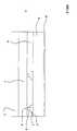
- Figure 1is a schematic sectional view of an integrated circuit according to the invention, in the area where the characteristic inductance is installed.
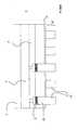
- Figure 2is a same sectional view made for a variant of production.
- Figure 3is the same sectional view made for another variant of production.
- FIGS 4 to 6are the same sectional views made for different steps of the process according to the invention.
- Figures 7 and 8are two same sectional views illustrating two variants different execution of the process according to the invention.
- the inventionrelates to an inductive component such as a coil or a transformer, incorporated in a monolithic integrated circuit.
- the integrated circuit (1)comprises a substrate (2) of semiconductor material, typically silicon or the like.
- the semiconductor substrate (2)includes an area active (3) having undergone different stages of growth and doping allowing the integrated circuit ensuring its electronic functions, as well as levels dedicated to the wiring between the different transistors or functions electronics made.
- This semiconductor substrate (2)is covered with a passivation layer (4), typically made of an alloy of oxide and nitride or any other passivator dielectric.
- This passivation layer (4)has a thickness of several microns. It is crossed by a plurality of metal contact pads (5), made in aluminum, and which allow connection to the semiconductor substrate (2) from the upper face (6) of the passivation layer (4).
- these contact pads (5)are flush with the face upper (6) of the passivation layer (4) occupying a surface close to a square (7) a few tens of microns aside.
- These studshave a section reduced (8) at the connection area with the active area (3) of the substrate semiconductor.
- the passivation layer (4)is covered with a polyimide layer (9).
- Polyimideis used in particular for its low electrical permittivity which limits the parasitic capacitance of the inductor according to the invention.
- This polyimide layer (9)has a thickness greater than 10 microns, and is preferably close to 30 microns.
- the polyimide layer (9)is crossed by segments (12) of a section close to that of the upper part (7) contact pads (5).
- These segments (12)are, according to the invention, made of copper.
- These segmentsconstitute the ends of the winding (20) forming inductance, and which is arranged above a layer of silica (16), itself disposed on the polyimide layer (9).
- the winding (20)forms a spiral, the geometry of which can be polygonal, or preferably circular.
- the segments (12) connected to the pads of contact (5)form downward extensions of the ends of the inductor (20), and typically from the end (21) of the outer coil and from the end central (22) of the spiral.
- the copper turns (21-23) of the windinghave a thickness greater than 10 microns, and preferably close to 30 microns.
- turns (21-23)follow a rectangular section, so as to present with respect to the adjacent turn a flat surface.
- the space between two faces (24, 25) of adjacent turnsis filled with air, which limits the parasitic capacity between turns.
- the distance between turnsis also close 30 microns.
- the copper coilsare covered with a layer of gold (29) or a gold-based alloy, of a similar thickness 1000 ⁇ .
- the space between the silica layer (16) and the passivation layer (4)is free of material, which limits the value of the parasitic capacitance between the coil (20) and the ground plane, thus than the capacity between turns (21-23).
- the inductor (20)rests on a layer of benzocyclobutene (10).
- This layer of benzocyclobutene (10)rests directly on the upper face (6) of the passivation layer.
- the benzocyclobuteneis chosen in particular for its low electrical permittivity which limits the parasitic capacitances between the inductance (20) and the passivation layer (4), as well as for its good resistance to humidity.
- the inventionrelates to a method for producing components as previously illustrated.
- the methodis carried out on an integrated circuit comprising a layer of semiconductor substrate (2) on which the active layer (3), and above which a layer of passivation (4) made of an alloy of oxide and nitride or any other passivator dielectric.
- This passivation layer (4)is crossed by metal studs (5) on the one hand, connected to the semiconductor substrate (2), and on the other hand, flush with the upper face (6) of the passivation layer (4).
- the first step of the process according to the inventionconsists in depositing a polyimide layer (9) on the passivation layer (4) of the entire wafer or the tablet previously formed, and generally called "wafer".
- a layer of silica (16)is deposited intended to ensure good attachment of metallic deposits on the upper face of the assembly.
- the passivation layeris covered with a layer of benzocyclobutene, chosen both for its low electrical permittivity, its planarizing power and its ability to receive metallic deposits.
- openings (30)are created inside the silica layers (16) and polyimide (9) so as to reveal the contact pads (5).
- a deposition of nickel (31)is carried out on the entire assembly and in particular above the contact pads (5).
- This nickel (31)is intended to serve as a barrier layer and to prohibit the migration of copper which will form the inductance towards the active area (3) of the semiconductor substrate (2).
- the layer of barrier metal (31), a second layer of metal (32) serving as a layer adaptationand typically made of nickel-gold or chrome-copper alloy.
- the barrier metal layerhas a thickness close to 2000 ⁇ .
- This second metal layer (32) or adaptation layerhas the function of limit the parasitic capacities which appear at the level of the metallic junctions and to promote intermetallic adhesion.
- This growth metal sublayeris made of chromium-copper alloy, and has a typical thickness of 2000 ⁇ .
- a photosensitive resinis deposited on the undercoat of growth metal (33). Then the resin is exposed according to the desired scheme and geometry of the inductor.
- the resinis then developed at the forms lines that will form the coil.
- the copper (35)is deposited by electrolytic growth, and from areas where the growth metal underlay is related.
- the copperis deposited to form the segments (23, 27, 28) forming the main part of the inductance. Electrolytic deposition of copper also takes place above the barrier layers (31) and adaptation (32) which have been deposited on the contact pads (5).
- the sides of the resinhave a height such that they channel the growth of copper, ensuring the verticality of the faces (24, 25) opposite the adjacent turns.
- a layeris deposited gold (29), typically 1000 ⁇ thick on copper coils (21-23, 27, 28), and more precisely on all the faces of these turns intended to come to the contact with the outside environment.
- this layer of gold (29) or of a gold-based alloyeliminates any risk of copper oxidation which would degrade the electrical performance of inductance.
- the method according to the inventionpresents an additional step intended to eliminate the layer of polyimide located between the planarization silica layer (16) and the passivation (4).
- This stepeliminates any material present between the inductance (20) and the integrated circuit proper, which improves the properties electrical by greatly reducing the values of stray capacitances both between inductance and mass, only between the turns of the inductance itself.
- the step of passivation of copper by a layer of goldis deposited after the polyimide has been removed, so that that the segments (12) of the inductor forming the ends of the coil are also covered with this protective gold layer (40).
- the inventionalso covers variants of the integrated circuit incorporating transformers consisting of several windings wound from nested within each other.
- the integrated circuit according to the inventionprovides electrical circuits incorporating inductors capable of operate at high frequencies, greater than several gigahertz, and having a quality factor far superior to existing circuits, typically by a factor of ten, and this throughout the frequency range.
- the method according to the inventionallows the manufacture of integrated circuits including inductive components without requiring major modifications of the manufacturing process, since inductors or inductive components are carried out directly following the manufacturing process of the integrated circuit well said.
- Such a processis also carried out at a temperature below 400 ° C., which avoids the risks of degradation of the active layer of the substrate.
- Integrated circuits according to the inventioncan find multiple applications, and in particular in all circuits including oscillators, amplifiers, mixers as well as in any active or passive filter.
Landscapes
- Physics & Mathematics (AREA)
- Condensed Matter Physics & Semiconductors (AREA)
- General Physics & Mathematics (AREA)
- Engineering & Computer Science (AREA)
- Computer Hardware Design (AREA)
- Microelectronics & Electronic Packaging (AREA)
- Power Engineering (AREA)
- Semiconductor Integrated Circuits (AREA)
Abstract
Translated fromFrenchDescription
Translated fromFrenchL'invention se rattache au domaine de la micro-électronique. Plusprécisément, elle concerne les circuits intégrés monolithiques incluant descomposants inductifs tels que ceux notamment utilisés pour des applications detélécommunications par radiofréquences.The invention relates to the field of microelectronics. Morespecifically, it relates to monolithic integrated circuits includinginductive components such as those used in particular forradio frequency telecommunications.
Elle concerne également un procédé de fabrication de tels composants, quipermet d'obtenir des circuits compacts et présentant des caractéristiquesélectriques, et notamment un facteur de qualité, supérieures à celles descomposants existant.It also relates to a process for manufacturing such components, whichprovides compact circuits with characteristicselectrics, and in particular a quality factor, superior to those ofexisting components.
Comme on le sait, les circuits intégrés sont de plus en plus utilisés dans lestechniques des micro-ondes et des radiofréquences.As we know, integrated circuits are used more and more inmicrowave and radio frequency techniques.
Dans ces applications, il est important de pouvoir utiliser des circuitsoscillants accordés, constitués par un ensemble capacité-inductance.In these applications, it is important to be able to use circuitstuned oscillators, made up of a capacitance-inductance unit.
Or, de tels circuits doivent être réalisés dans des volumes de plus en plusréduits. En outre, ils doivent fonctionner à des fréquences de plus en plus élevées.Par conséquent, la consommation électrique de tels composants devient unparamètre critique, par exemple dans les téléphones portables cellulaires, car laconsommation influe directement sur l'autonomie de ces appareils.However, such circuits must be carried out in increasingly large volumesreduced. In addition, they must operate at increasingly higher frequencies.Therefore, the power consumption of such components becomes acritical parameter, for example in cellular mobile phones, because theconsumption directly influences the autonomy of these devices.
Ainsi, il est demandé aux composants passifs constituant les filtres utilisésdans les systèmes radiofréquences, et notamment les inductances, d'occuper unesurface aussi faible que possible à l'intérieur des circuits intégrés, de présenter une valeur d'inductance aussi élevée que possible, et d'induire une consommationélectrique aussi faible que possible.Thus, the passive components constituting the filters used are askedin radio frequency systems, and in particular inductances, to occupy asurface as small as possible inside integrated circuits, to present aInductance value as high as possible, and to induce consumptionas low as possible.
En outre, on sait que les inductances implantées à l'intérieur de circuitsintégrés en matériau semi-conducteur subissent l'influence de capacités parasitesconstituées par les différentes zones de substrat localisées au voisinage desinductances.In addition, we know that the inductors installed inside circuitsintegrated in semiconductor material are influenced by stray capacitancesformed by the different substrate zones located in the vicinity ofinductors.
Ainsi, en pratique, une inductance présente un schéma équivalent dans lequel,à cette inductance proprement dite, s'ajoutent différents composants parasitesécartant cette inductance de son comportement idéal.Thus, in practice, an inductor presents an equivalent diagram in which,to this actual inductance are added various parasitic componentsremoving this inductance from its ideal behavior.
Ainsi, une inductance réelle présente une résistance correspondant à celle dumétal qui la compose.Thus, a real inductance has a resistance corresponding to that of themetal that composes it.
En outre, le comportement électrique de l'inductance est perturbé par descapacités parasites qui résultent de différentes couches de matériaux de mauvaisepermittivité électrique, situées au-dessus du substrat.In addition, the electrical behavior of the inductor is disturbed bystray capacitances that result from different layers of bad materialselectrical permittivity, located above the substrate.
En outre, aux capacités parasites de ces différentes couches, s'ajoutent unecapacité et une résistance parasite correspondant à l'influence du substrat semi-conducteursitué au dessus du plan de masse.In addition, to the parasitic capacities of these different layers, there is added acapacitance and parasitic resistance corresponding to the influence of the semiconductor substratelocated above the ground plane.
En outre, une capacité parasite existe entre les différentes spires constituantl'inductance.In addition, a parasitic capacity exists between the different turns constitutinginductance.
Dans le document EP 0 969 509, Le Demandeur a décrit une solutionpermettant de réaliser de telles inductances sur un substrat semi-conducteur, enadoptant une disposition permettant de réduire fortement la valeur de la capacitéparasite existant entre spires. Une telle solution consiste à réaliser l'inductance parun ruban métallique déposé sur le substrat, et à graver ledit substrat pour ménager une cavité en dessous du ruban formant inductance, et ainsi à suspendre et éloignerl'inductance du substrat.In document EP 0 969 509, The Applicant has described a solutionmaking it possible to produce such inductances on a semiconductor substrate,adopting a provision making it possible to greatly reduce the value of capacityparasite existing between turns. One such solution consists in carrying out the inductance bya metallic ribbon deposited on the substrate, and to etch said substrate to sparea cavity below the ribbon forming an inductor, and thus to be suspended and removedthe inductance of the substrate.
Grâce à ces dispositions, il est possible d'utiliser des inductances à desfréquences plus élevées tout en conservant un comportement satisfaisant. Onrappelle que la fréquence optimale de fonctionnement est déterminée comme étantcelle où le facteur de qualité est maximum. Le facteur de qualité est déterminé defaçon connue par le rapport entre la partie imaginaire ou réactance, et la partieréelle de l'impédance d'entrée d'une inductance.Thanks to these provisions, it is possible to use inductors athigher frequencies while maintaining satisfactory behavior. Werecalls that the optimal operating frequency is determined to bethe one where the quality factor is maximum. The quality factor is determined fromknown way by the relation between the imaginary part or reactance, and the partreal of the input impedance of an inductor.
La solution décrite dans le document précité, bien que satisfaisante, ne permetpas d'améliorer de façon notable, le facteur de qualité dans les plages de fréquencesbasses, c'est-à-dire situées en dessous de la moitié de la fréquence optimale, qui estdans les applications typiques de l'invention, proche de quelques gigahertz.The solution described in the aforementioned document, although satisfactory, does not allownot significantly improve the quality factor in the frequency rangesbass, that is, located below half the optimal frequency, which isin typical applications of the invention, close to a few gigahertz.
En effet, dans cette gamme de fréquence, le comportement de l'inductance estfortement dépendant de la valeur de la résistance équivalente, qui correspond à larésistance électrique du ruban métallique constituant l'inductance proprement dite.Indeed, in this frequency range, the behavior of the inductance isstrongly dependent on the value of the equivalent resistance, which corresponds to theelectrical resistance of the metallic strip constituting the inductance proper.
Or, toutes les inductances réalisées dans les circuits intégrés, sont aujourd'huiconstituées d'aluminium, et présentent des dimensions faibles, et surtout uneépaisseur très faible, typiquement inférieure à 4 microns, ce qui se traduit par unerésistance électrique élevée.However, all the inductances made in integrated circuits are todaymade of aluminum, and have small dimensions, and above all avery small thickness, typically less than 4 microns, which results in ahigh electrical resistance.
Ainsi, un des problèmes que se propose de résoudre l'invention est celui del'influence néfaste de la résistance globale de l'enroulement formant inductance,tout en conservant des caractéristiques électriques avantageuses, notamment entermes de capacité parasite.Thus, one of the problems which the invention proposes to solve is that ofthe harmful influence of the overall resistance of the inductance winding,while retaining advantageous electrical characteristics, in particular byparasitic capacity terms.
De nombreux documents, tels que notamment les documents US 5 874 883,EP 0 782 190 ou US 5 834 825, décrivent des circuits intégrés qui comportent à leur surface des inductances constituées d'un ruban métallique. Ces dispositifsprésentent les avantages précités concernant un faible facteur de qualité lorsque leruban métallique est d'épaisseur classique, de l'ordre de quelques microns. Enoutre, ces inductances sont réalisées pendant le procédé de fabrication du circuitintégré proprement dit, ce qui augmente les contraintes technologiques car leurimplantation doit être prise en compte dans les étapes du procédé. Enfin et surtout,de telles inductances occupent une certaine surface sur le substrat semi-conducteur.Cette surface utilisée par l'inductance ne peut donc pas servir à implanter des zonesactives dans le semi-conducteur, ce qui diminue la densité utile de ce dernier.Numerous documents, such as in particular documents US 5,874,883,EP 0 782 190 or US 5 834 825, describe integrated circuits which includetheir surface of the inductors constituted by a metallic ribbon. These deviceshave the aforementioned advantages regarding a low quality factor when themetal tape is of conventional thickness, of the order of a few microns. Inin addition, these inductors are produced during the circuit manufacturing processintegrated itself, which increases technological constraints because theirimplantation must be taken into account in the process steps. Finally and especially,such inductors occupy a certain surface on the semiconductor substrate.This surface used by the inductor cannot therefore be used to implant zonesactive in the semiconductor, which decreases the useful density of the latter.
Dans le document US 5 478 773, on a proposé de réaliser une inductance surun substrat, en formant un ruban de cuivre par attaque chimique d'une couche decuivre. Malheureusement, pour former les spires de l'inductance, il est nécessairede procéder à un premier dépôt d'une couche de croissance de cuivre pulvérisé,puis d'une seconde couche de cuivre électrolytique. On procède ensuite à unegravure différentielle qui attaque préférentiellement le cuivre pulvérisé par rapportau cuivre électrolytique. Cette gravure différentielle est nécessaire pour ne pasendommager les parties de cuivre électrolytique qui forment les spires. De tellesprécautions opératoires compliquent le procédé et ne permettent pas d'obtenir desspires de taille suffisante pour améliorer nettement le facteur de qualité.In document US 5,478,773, it has been proposed to produce an inductor ona substrate, forming a copper ribbon by chemical attack on a layer ofcopper. Unfortunately, to form the inductance turns, it is necessaryto carry out a first deposit of a growth layer of pulverized copper,then a second layer of electrolytic copper. We then proceed to adifferential etching which preferentially attacks the sprayed copper compared towith electrolytic copper. This differential etching is necessary so as not todamage the parts of electrolytic copper which form the turns. Suchoperating precautions complicate the process and do not allow obtainingcoils of sufficient size to significantly improve the quality factor.
L'invention concerne donc un circuit intégré monolithique incorporant uncomposant inductif, et comprenant :
- une couche de substrat semi-conducteur ;
- une couche de passivation recouvrant la couche de substrat ;
- des plots de contact métalliques connectés au substrat et traversant lacouche de passivation pour affleurer sur la face supérieure de la couche.
- a layer of semiconductor substrate;
- a passivation layer covering the substrate layer;
- metallic contact pads connected to the substrate and passing through the passivation layer to be flush with the upper face of the layer.
Ce circuit intégré secaractérise en ce qu'il comporte également unenroulement en spirale formant inductance, et disposé selon un plan parallèle à la face supérieure de la couche de passivation, ledit enroulement étant constitué despires en cuivre présentant une épaisseur supérieure à 10 microns, les extrémités del'enroulement formant des prolongements s'étendant sous le plan de l'enroulement,et étant connectées aux plots de contact.This integrated circuit ischaracterized in that it also comprises a spiral winding forming an inductor, and arranged in a plane parallel to the upper face of the passivation layer, said winding consisting of copper turns having a thickness greater than 10 microns , the ends of the winding forming extensions extending under the plane of the winding, and being connected to the contact pads.
Autrement dit, l'inductance est montée directement sur le circuit intégré, au-dessusde la couche de passivation. Elle est formée juste après le processus deréalisation du circuit intégré lui-même. Il est donc possible de la créer sur deswafers de provenance très diverse, puisque sa réalisation est dissociée desopérations de fabrication du circuit intégré proprement dit.In other words, the inductor is mounted directly on the integrated circuit, aboveof the passivation layer. It is formed right after the process ofrealization of the integrated circuit itself. It is therefore possible to create it onwafers of very diverse provenance, since its realization is dissociated frommanufacturing operations of the integrated circuit proper.
Une telle inductance est disposée au dessus du circuit intégré et non pas sur lecircuit intégré, de sorte que la surface du circuit intégré située à l'aplomb del'inductance peut comprendre des zones actives en plus des plots de contact. Ladensité de fonctions sur le circuit intégré n'est donc pas diminuée par la présencede l'inductance.Such an inductor is placed above the integrated circuit and not on theintegrated circuit, so that the surface of the integrated circuit located belowthe inductance may include active zones in addition to the contact pads. Thedensity of functions on the integrated circuit is therefore not reduced by the presenceinductance.
L'utilisation de cuivre pour la réalisation de l'enroulement permet de diminuertrès fortement la résistance équivalente de l'inductance. Cette réduction est encoreaccentuée par l'utilisation de spires d'épaisseur largement supérieure à celle desrubans métalliques actuellement utilisés.The use of copper for the winding reducesvery strongly the equivalent resistance of the inductor. This reduction is stillaccentuated by the use of coils of thickness much greater than that ofmetallic ribbons currently used.
De la sorte, la résistance équivalente est très fortement réduite, typiquementd'un facteur dix par rapport à la résistance des inductances aujourd'hui réaliséesdans les circuits intégrés.In this way, the equivalent resistance is very greatly reduced, typicallyby a factor of ten compared to the resistance of the inductors today madein integrated circuits.
Il s'ensuit que le facteur qualité est très largement supérieur à celui desinductances aujourd'hui existantes, et notamment dès les basses fréquences.It follows that the quality factor is very much higher than that oftoday existing inductors, especially from low frequencies.
Typiquement, le facteur de qualité de telles bobines est supérieur d'un facteurenviron dix au facteur de qualité des inductances existantes.Typically, the quality factor of such coils is greater by a factorabout ten to the quality factor of existing inductors.
Avantageusement en pratique, le plan selon lequel est disposé l'inductance estdistant de la face supérieure de la couche de passivation, d'une distance supérieureà 10 microns.Advantageously in practice, the plane according to which the inductance is arranged isdistant from the upper face of the passivation layer, by a greater distanceat 10 microns.
En effet, on a constaté qu'il est important que l'inductance proprement ditesoit suffisamment éloignée du substrat pour limiter les phénomènes de pertesélectriques à l'intérieur du substrat, observées aux fréquences de fonctionnementdes circuits selon l'invention. Cette distance ne doit pas néanmoins être tropgrande, au risque de déstabiliser mécaniquement l'inductance.Indeed, it has been found that it is important that the inductance properis sufficiently distant from the substrate to limit the loss phenomenaelectric inside the substrate, observed at operating frequenciescircuits according to the invention. However, this distance should not be toolarge, at the risk of mechanically destabilizing the inductance.
Ainsi, pour une distance supérieure à 10 microns, et préférentiellementvoisine de 30 microns, on limite les pertes électriques dans le substrat tout enassurant une bonne stabilité mécanique.Thus, for a distance greater than 10 microns, and preferablyclose to 30 microns, we limit the electrical losses in the substrate whileensuring good mechanical stability.
Dans une première variante de réalisation, le composant comprend unecouche de support en benzocyclobutène sur laquelle repose l'enroulement formantinductance. De la sorte, l'inductance est stabilisée mécaniquement sur la couche desupport, ce qui évite aux différentes spires de l'inductance de vibrer les unes parrapport aux autres, ce qui assure une bonne rigidité mécanique.In a first alternative embodiment, the component comprises abenzocyclobutene support layer on which the winding restsinductance. In this way, the inductance is mechanically stabilized on the layer ofsupport, which prevents the different turns of the inductance from vibrating with each othercompared to others, which ensures good mechanical rigidity.
Dans une seconde variante de réalisation, la couche de support sur laquellerepose l'enroulement formant inductance est réalisée en silice .Selon deux formesd'exécution, la couche de support en silice est séparée de la face supérieure de lacouche de passivation
soit par une couche de polyimide, ou tout autre polymère diélectrique;
soit par une couche d'air.In a second variant, the support layer on which the inductance winding rests is made of silica. According to two embodiments, the support layer of silica is separated from the upper face of the passivation layer.
either by a layer of polyimide, or any other dielectric polymer;
either by a layer of air.
Dans cette dernière forme d'exécution, les propriétés électriques sontoptimisées puisque la permittivité électrique de l'air est inférieure à celle dupolyimide.In this latter embodiment, the electrical properties areoptimized since the electrical permittivity of the air is lower than that of thepolyimide.
Selon une autre caractéristique de l'invention, l'enroulement en cuivre peutêtre recouvert d'une couche d'or ou d'alliage à base d'or, destinée à assurer lapassivation du cuivre, et à interdire les phénomènes d'oxydation du cuivre quiviendraient en dégrader les caractéristiques de résistance électrique, notammentdans le cas où le circuit intégré est utilisé dans des atmosphères humides, voirechimiquement agressives.According to another characteristic of the invention, the copper winding canbe covered with a layer of gold or gold-based alloy, intended to ensure thepassivation of copper, and to prohibit the oxidation phenomena of copper whichwould degrade the characteristics of electrical resistance, in particularin the case where the integrated circuit is used in humid atmospheres, evenchemically aggressive.
Selon une autre caractéristique de l'invention, l'espace entre deux spiresconsécutives de l'enroulement est exempt de matière, ou plus précisément emplid'air, ce qui diminue fortement la capacité parasite existant entre chaque spire, etaugmente donc la fréquence optimale de fonctionnement de l'inductance.According to another characteristic of the invention, the space between two turnsof the winding is free of material, or more precisely filledair, which greatly reduces the parasitic capacity existing between each turn, andtherefore increases the optimal operating frequency of the inductor.
Comme déjà dit, l'invention concerne également un procédé de fabricationd'un circuit intégré monolithique incorporant un composant inductif. Ainsi, à partird'un substrat semi-conducteur recouvert d'une couche de passivation, etcomprenant des plots métalliques connectés au substrat, et traversant la couche depassivation pour affleurer sur la face supérieure de ladite couche, le procédéconforme à l'invention secaractérise en ce qu'il comprend les étapes suivantes,dans lesquelles :
- on dépose une couche de polyimide sur la couche de passivation ;
- on dépose une couche de silice sur ladite couche de polyimide ;
- on aménage des ouvertures dans les couches de silice et de polyimide, lesdites ouvertures débouchant sur les plots métalliques ;
- on dépose sur l'ensemble une sous-couche de métal de croissance ;
- on dépose sur la sous-couche de métal de croissance, une couche de résinephotosensible ;
- on insole la résine et on élimine les zones destinées à former la faceinférieure du composant inductif ;
- on dépose par électrolyse sur les zones apparentes de la sous-couche demétal de croissance, une couche de cuivre destinée à former le ruban ducomposant inductif ;
- on élimine le reste de la résine photosensible et la sous-couche de métal decroissance.
- a layer of polyimide is deposited on the passivation layer;
- a layer of silica is deposited on said polyimide layer;
- openings are arranged in the layers of silica and polyimide, the said openings opening onto the metal studs;
- a growth metal sublayer is deposited on the assembly;
- a layer of photosensitive resin is deposited on the growth metal sublayer;
- the resin is exposed and the areas intended to form the underside of the inductive component are eliminated;
- a layer of copper intended to form the ribbon of the inductive component is deposited by electrolysis on the visible areas of the growth metal sublayer;
- the rest of the photosensitive resin and the growth metal underlay are removed.
Autrement dit, le procédé conforme à l'invention permet de réaliserdirectement sur le circuit intégré, les inductances nécessaires au bonfonctionnement du circuit, à la suite du processus de fabrication du circuit intégréproprement dit.In other words, the method according to the invention makes it possible to carry outdirectly on the integrated circuit, the inductors necessary for correctcircuit operation, following the integrated circuit manufacturing processwell said.
De la sorte, les enroulements des inductances sont toutes réaliséessimultanément, au cours d'une série d'étapes constituant une prolongation duprocédé de fabrication du circuit intégré lui-même. Il n'est donc pas nécessaire defaire appel à des opérations de report ultérieur qui consisteraient à connecter desinductances réalisées par ailleurs sur un circuit intégré fini.In this way, the windings of the inductors are all madesimultaneously, during a series of steps constituting an extension of themanufacturing process of the integrated circuit itself. There is therefore no need touse carry-over operations which would consist in connectinginductors also made on a finite integrated circuit.
Selon une variante de réalisation, le procédé comporte une étapesupplémentaire d'élimination de la couche de polyimide, aboutissant à uncomposant dont l'inductance est suspendue au-dessus de la couche de passivation.According to an alternative embodiment, the method comprises a stepadditional removal of the polyimide layer, resulting in acomponent whose inductance is suspended above the passivation layer.
Bien évidemment, l'invention couvre également le procédé dans lequel lacouche de polyimide est conservée pour notamment assurer une stabilité del'inductance.Obviously, the invention also covers the process in which thepolyimide layer is preserved in particular to ensure a stability ofinductance.
Selon une variante de réalisation, les deux couches de polyimide et de silicesont remplacées par une unique couche de benzocyclobutène, ou tout autrematériau équivalent à très faible constante diélectrique.According to an alternative embodiment, the two layers of polyimide and silicaare replaced by a single layer of benzocyclobutene, or any othermaterial equivalent to very low dielectric constant.
Comme déjà dit, le procédé peut également inclure une étape de passivationdu ruban de cuivre par dépôt d'une couche d'or, ou d'alliage à base d'or.Néanmoins, dans une mise en oeuvre moins perfectionnée du procédé, on peutprévoir de recouvrir les spires d'une simple couche de passivation classique.As already said, the process can also include a passivation stepcopper tape by depositing a layer of gold, or a gold-based alloy.However, in a less perfected implementation of the process, one canplan to cover the turns with a simple layer of conventional passivation.
Avantageusement en pratique, le procédé peut inclure une étape de dépôt d'unmétal formant couche barrière sur le plot métallique. De la sorte, on élimine lesphénomènes de migration du cuivre en direction de l'aluminium, dont on sait qu'ilspeuvent induire des dégradations de la couche active du substrat semi-conducteur.Advantageously in practice, the method can include a step of depositing ametal forming barrier layer on the metal pad. In this way, we eliminate thecopper migration phenomena towards aluminum, which we know to becan induce degradation of the active layer of the semiconductor substrate.
Avantageusement, le procédé comporte postérieurement à l'étape de dépôt dela couche barrière, une étape de dépôt d'une couche d'adaptation sur la couche demétal barrière. Cette étape permet d'optimiser le contact et favorise l'adhérenceintermetallique tout en limitant les capacités parasites apparaissant au niveau desjonctions métalliques.Advantageously, the method comprises after the step of depositingthe barrier layer, a step of depositing an adaptation layer on the layer ofmetal barrier. This step optimizes contact and promotes adhesionintermetallic while limiting the parasitic capacities appearing at the level ofmetal junctions.
La manière de réaliser l'invention ainsi que les avantages qui en découlentressortiront bien de la description des modes de réalisation qui suivent, à l'appuides figures annexées, dans lesquelles :The manner of carrying out the invention as well as the advantages which flow therefromwill emerge clearly from the description of the embodiments which follow, in supportappended figures, in which:
La figure 1 est une vue en coupe schématique d'un circuit intégré conforme àl'invention, dans la zone où est implantée l'inductance caractéristique.Figure 1 is a schematic sectional view of an integrated circuit according tothe invention, in the area where the characteristic inductance is installed.
La figure 2 est une même vue en coupe réalisée pour une variante deréalisation.Figure 2 is a same sectional view made for a variant ofproduction.
La figure 3 est une même vue en coupe réalisée pour une autre variante deréalisation.Figure 3 is the same sectional view made for another variant ofproduction.
Les figures 4 à 6 sont des mêmes vues en coupe réalisées pour différentesétapes du procédé conforme à l'invention.Figures 4 to 6 are the same sectional views made for differentsteps of the process according to the invention.
Les figures 7 et 8 sont deux mêmes vues en coupe illustrant deux variantesdifférentes d'exécution du procédé conforme à l'invention.Figures 7 and 8 are two same sectional views illustrating two variantsdifferent execution of the process according to the invention.
Comme déjà dit, l'invention concerne un composant inductif tel qu'une bobineou un transformateur, incorporé dans un circuit intégré monolithique.As already said, the invention relates to an inductive component such as a coilor a transformer, incorporated in a monolithic integrated circuit.
Ainsi, comme illustré à la figure 1, le circuit intégré (1) comporte unsubstrat (2) en matériau semi-conducteur, typiquement du silicium ou analogue.Thus, as illustrated in FIG. 1, the integrated circuit (1) comprises asubstrate (2) of semiconductor material, typically silicon or the like.
Dans sa partie supérieure le substrat semi-conducteur (2) inclut une zoneactive (3) ayant subi différentes étapes de croissance et de dopage permettant aucircuit intégré d'assurer ses fonctions électroniques, ainsi que des niveauxmétalliques dédiés au cablage entre les différents transistors ou fonctionsélectroniques réalisées.In its upper part the semiconductor substrate (2) includes an areaactive (3) having undergone different stages of growth and doping allowing theintegrated circuit ensuring its electronic functions, as well as levelsdedicated to the wiring between the different transistors or functionselectronics made.
Ce substrat semi-conducteur (2) est recouvert d'une couche de passivation (4),typiquement constituée en un alliage d'oxyde et de nitrure ou tout autre passivantdiélectrique. Cette couche de passivation (4) a une épaisseur de plusieurs microns.Elle est traversée par une pluralité de plots de contact métalliques (5), réalisés enaluminium, et qui permettent la connexion au substrat semi-conducteur (2) depuisla face supérieure (6) de la couche de passivation (4).This semiconductor substrate (2) is covered with a passivation layer (4),typically made of an alloy of oxide and nitride or any other passivatordielectric. This passivation layer (4) has a thickness of several microns.It is crossed by a plurality of metal contact pads (5), made inaluminum, and which allow connection to the semiconductor substrate (2) fromthe upper face (6) of the passivation layer (4).
Ainsi, en pratique, ces plots de contact (5) affleurent au niveau de la facesupérieure (6) de la couche de passivation (4) en occupant une surface proche d'uncarré (7) de quelques dizaines de microns de côté. Ces plots présentent une sectionréduite (8) au niveau de la zone de connexion avec la zone active (3) du substratsemi-conducteur.Thus, in practice, these contact pads (5) are flush with the faceupper (6) of the passivation layer (4) occupying a surface close to asquare (7) a few tens of microns aside. These studs have a sectionreduced (8) at the connection area with the active area (3) of the substratesemiconductor.
Conformément à l'invention, dans la forme de réalisation illustrée à lafigure 1, la couche de passivation (4) est recouverte d'une couche de polyimide (9).According to the invention, in the embodiment illustrated in theFigure 1, the passivation layer (4) is covered with a polyimide layer (9).
Le polyimide est notamment utilisé pour sa faible permittivité électrique quilimite la capacité parasite de l'inductance conforme à l'invention.Polyimide is used in particular for its low electrical permittivity whichlimits the parasitic capacitance of the inductor according to the invention.
Cette couche de polyimide (9) a une épaisseur supérieure à 10 microns, et estpréférentiellement voisine de 30 microns.This polyimide layer (9) has a thickness greater than 10 microns, and ispreferably close to 30 microns.
Au niveau de l'aplomb des plots de contact (5), la couche de polyimide (9) esttraversée par des segments (12) d'une section voisine à celle de la partie supérieure(7) des plots de contact (5). Ces segments (12) sont, conformément à l'invention,réalisés en cuivre.At the level of the contact pads (5), the polyimide layer (9) iscrossed by segments (12) of a section close to that of the upper part(7) contact pads (5). These segments (12) are, according to the invention,made of copper.
Ces segments constituent les extrémités de l'enroulement (20) formantinductance, et qui est disposé au-dessus d'une couche de silice (16), elle-mêmedisposée sur la couche de polyimide (9).These segments constitute the ends of the winding (20) forminginductance, and which is arranged above a layer of silica (16), itselfdisposed on the polyimide layer (9).
L'enroulement (20) forme une spirale, dont la géométrie peut être polygonale,ou préférentiellement circulaire. Ainsi, les segments (12) connectés aux plots decontact (5) forment des prolongements vers le bas des extrémités de l'inductance(20), et typiquement de l'extrémité (21) de la spire extérieure et de l'extrémitécentrale (22) de la spirale.The winding (20) forms a spiral, the geometry of which can be polygonal,or preferably circular. Thus, the segments (12) connected to the pads ofcontact (5) form downward extensions of the ends of the inductor(20), and typically from the end (21) of the outer coil and from the endcentral (22) of the spiral.
Avantageusement en pratique, les spires en cuivre (21-23) de l'enroulementprésentent une épaisseur supérieure à 10 microns, et de préférence voisine de 30microns.Advantageously in practice, the copper turns (21-23) of the windinghave a thickness greater than 10 microns, and preferably close to 30microns.
Ces spires (21-23) épousent une section rectangulaire, de manière à présentervis à vis de la spire adjacente une surface plane. L'espace entre deux faces (24, 25)de spires adjacentes est empli d'air, ce qui limite la capacité parasite entre spires.These turns (21-23) follow a rectangular section, so as to presentwith respect to the adjacent turn a flat surface. The space between two faces (24, 25)of adjacent turns is filled with air, which limits the parasitic capacity between turns.
Avantageusement en pratique, la distance entre spires est également voisinede 30 microns.Advantageously in practice, the distance between turns is also close30 microns.
Compte tenu des risques d'oxydation inhérents au fonctionnement enatmosphère humide ou chimiquement agressive, les spires de cuivre sontrecouvertes d'une couche d'or (29) ou d'alliage à base d'or, d'une épaisseur voisinede 1000 Å.Given the risks of oxidation inherent in operation inhumid or chemically aggressive atmosphere, the copper coils arecovered with a layer of gold (29) or a gold-based alloy, of a similar thickness1000 Å.
Dans la variante de réalisation illustrée à la figure 2, l'espace compris entre lacouche de silice (16) et la couche de passivation (4) est exempt de matière, ce quilimite la valeur de la capacité parasite entre la bobine (20) et le plan de masse, ainsique la capacité entre spires (21-23).In the variant embodiment illustrated in FIG. 2, the space between thesilica layer (16) and the passivation layer (4) is free of material, whichlimits the value of the parasitic capacitance between the coil (20) and the ground plane, thusthan the capacity between turns (21-23).
Dans la forme de réalisation illustrée à la figure 3, l'inductance (20) reposesur une couche de benzocyclobutène (10). Cette couche de benzocyclobutène (10)repose directement sur la face supérieure (6) de la couche de passivation. (4). Lebenzocyclobutène est choisi notamment pour sa faible permittivité électrique quilimite les capacités parasites entre l'inductance (20) et la couche de passivation (4),ainsi que pour sa bonne tenue à l'humidité.In the embodiment illustrated in Figure 3, the inductor (20) restson a layer of benzocyclobutene (10). This layer of benzocyclobutene (10)rests directly on the upper face (6) of the passivation layer. (4). Thebenzocyclobutene is chosen in particular for its low electrical permittivity whichlimits the parasitic capacitances between the inductance (20) and the passivation layer (4),as well as for its good resistance to humidity.
Comme déjà dit, l'invention concerne un procédé de réalisation decomposants tels que précédemment illustrés.As already said, the invention relates to a method for producingcomponents as previously illustrated.
Ainsi, comme illustré à la figure 4, le procédé est réalisé sur un circuit intégrécomprenant une couche de substrat semi-conducteur (2) sur laquelle a été formée lacouche active (3), et au-dessus de laquelle a été déposée une couche depassivation (4) réalisée en un alliage d'oxyde et de nitrure ou tout autre passivantdiélectrique.Thus, as illustrated in FIG. 4, the method is carried out on an integrated circuitcomprising a layer of semiconductor substrate (2) on which theactive layer (3), and above which a layer ofpassivation (4) made of an alloy of oxide and nitride or any other passivatordielectric.
Cette couche de passivation (4) est traversée par des plots métalliques (5)d'une part, connectés au substrat semi-conducteur (2), et d'autre part, affleurant à laface supérieure (6) de la couche de passivation (4).This passivation layer (4) is crossed by metal studs (5)on the one hand, connected to the semiconductor substrate (2), and on the other hand, flush with theupper face (6) of the passivation layer (4).
Ainsi, la première étape du procédé conforme à l'invention consiste à déposerune couche de polyimide (9) sur la couche de passivation (4) de la totalité de lagalette ou la pastille préalablement formée, et généralement dénommée "wafer".Thus, the first step of the process according to the invention consists in depositinga polyimide layer (9) on the passivation layer (4) of the entirewafer or the tablet previously formed, and generally called "wafer".
Après avoir déposé la couche de polyimide (9) sur une épaisseur de 30microns environ, on dépose une couche de silice (16) destinée à assurer un bonaccrochage des dépôts métalliques sur la face supérieure de l'ensemble.After having deposited the polyimide layer (9) to a thickness of 30approximately microns, a layer of silica (16) is deposited intended to ensure goodattachment of metallic deposits on the upper face of the assembly.
Selon une autre variante d'exécution aboutissant au circuit illustré à lafigure 3, la couche de passivation est recouverte d'une couche debenzocyclobutène, choisi à la fois pour sa faible permittivité électrique, sonpouvoir planarisant et son aptitude à recevoir les dépôts métalliques.According to another alternative embodiment leading to the circuit illustrated inFigure 3, the passivation layer is covered with a layer ofbenzocyclobutene, chosen both for its low electrical permittivity, itsplanarizing power and its ability to receive metallic deposits.
Par la suite, on crée des ouvertures (30) à l'intérieur des couches de silice (16)et de polyimide (9) de manière à laisser apparaítre les plots de contact (5).Subsequently, openings (30) are created inside the silica layers (16)and polyimide (9) so as to reveal the contact pads (5).
Selon une caractéristique de l'invention, on réalise un dépôt de nickel (31) surla totalité de l'ensemble et notamment au-dessus des plots de contact (5). Ce nickel(31) est destiné à servir de couche barrière et interdire la migration du cuivre quiformera l'inductance en direction de la zone active (3) du substrat semi-conducteur(2).According to a characteristic of the invention, a deposition of nickel (31) is carried out onthe entire assembly and in particular above the contact pads (5). This nickel(31) is intended to serve as a barrier layer and to prohibit the migration of copper whichwill form the inductance towards the active area (3) of the semiconductor substrate(2).
Selon une autre caractéristique de l'invention, on dépose sur la couche demétal barrière (31), une seconde couche de métal (32) servant de couched'adaptation, et typiquement réalisée en alliage nickel-or ou chrome-cuivre.According to another characteristic of the invention, the layer ofbarrier metal (31), a second layer of metal (32) serving as a layeradaptation, and typically made of nickel-gold or chrome-copper alloy.
Typiquement, la couche de métal barrière présente une épaisseur voisine de2000 Å.Typically, the barrier metal layer has a thickness close to2000 Å.
Cette seconde couche de métal (32) ou couche d'adaptation a pour fonction delimiter les capacités parasites qui apparaissent au niveau des jonctions métalliqueset de favoriser l'adhésion intermétallique.This second metal layer (32) or adaptation layer has the function oflimit the parasitic capacities which appear at the level of the metallic junctionsand to promote intermetallic adhesion.
Ensuite, conformément à l'invention on réalise le dépôt d'une sous-couche demétal de croissance (33) sur la totalité de l'ensemble, pour aboutir à la formeillustrée à la figure 5. Cette sous-couche de métal de croissance est réalisée enalliage de chrome-cuivre, et présente une épaisseur typique de 2000 Å.Then, in accordance with the invention, a sub-layer ofgrowth metal (33) over the entire assembly, to formillustrated in Figure 5. This growth metal sublayer is made ofchromium-copper alloy, and has a typical thickness of 2000 Å.
Par la suite, on procède au dépôt d'une résine photosensible sur la sous-couchede métal de croissance (33). On insole ensuite la résine en fonction duschéma souhaité et de la géométrie de l'inductance.Subsequently, a photosensitive resin is deposited on the undercoatof growth metal (33). Then the resin is exposed according to thedesired scheme and geometry of the inductor.
Ainsi, en fonction du masque choisi, la résine est ensuite développée à laforme des lignes qui formeront l'enroulement.Thus, depending on the mask chosen, the resin is then developed at theforms lines that will form the coil.
Par la suite, on procède au dépôt du cuivre (35) par croissance électrolytique,et à partir des zones dans lesquelles la sous-couche de métal de croissance estapparente.Thereafter, the copper (35) is deposited by electrolytic growth,and from areas where the growth metal underlay isrelated.
Au niveau de la couche de silice de planarisation (16) le cuivre se déposepour former les segments (23, 27, 28) formant la principale partie de l'inductance.Le dépôt électrolytique de cuivre a également lieu au-dessus des couches barrière(31) et d'adaptation (32) qui ont été déposées sur les plots de contact (5).At the level of the planarization silica layer (16) the copper is depositedto form the segments (23, 27, 28) forming the main part of the inductance.Electrolytic deposition of copper also takes place above the barrier layers(31) and adaptation (32) which have been deposited on the contact pads (5).
Les flancs de la résine présentent une hauteur telle qu'ils canalisent lacroissance du cuivre, en garantissant la verticalité des faces (24, 25) en regard desspires adjacentes.The sides of the resin have a height such that they channel thegrowth of copper, ensuring the verticality of the faces (24, 25) opposite theadjacent turns.
Lorsque les spires de cuivre (21-23, 27, 28) déposées électrolytiquementatteignent la hauteur voulue, soit environ 30 microns, on procède ensuite àl'élimination de la résine restante ainsi que de la sous-couche de métal decroissance qui était protégée par ladite résine, pour aboutir à l'état illustré à lafigure 6.When the copper turns (21-23, 27, 28) electrolytically depositedreach the desired height, about 30 microns, then proceed toremoval of the remaining resin as well as the metal undercoat ofgrowth which was protected by said resin, to reach the state illustrated in thefigure 6.
Par la suite, comme illustré à la figure 7, on procède à un dépôt d'une couched'or (29), typiquement d'une épaisseur de 1000 Å sur les spires de cuivre (21-23,27, 28), et plus précisément sur toutes les faces de ces spires destinées à venir aucontact avec le milieu extérieur.Thereafter, as illustrated in FIG. 7, a layer is depositedgold (29), typically 1000 Å thick on copper coils (21-23,27, 28), and more precisely on all the faces of these turns intended to come to thecontact with the outside environment.
Le dépôt de cette couche d'or (29) ou d'alliage à base d'or, permet d'éliminertout risque d'oxydation du cuivre qui dégraderait les performances électriques del'inductance.The deposition of this layer of gold (29) or of a gold-based alloy eliminatesany risk of copper oxidation which would degrade the electrical performance ofinductance.
On obtient ainsi l'inductance telle qu'illustrée à la figure 7, correspondantsensiblement à l'inductance de la figure 1.The inductance is thus obtained as illustrated in FIG. 7, correspondingsubstantially at the inductance of figure 1.
Dans une variante de réalisation illustrée à la figure 8, le procédé conforme àl'invention présente une étape supplémentaire destinée à éliminer la couche depolyimide située entre la couche de silice de planarisation (16) et la couche depassivation (4). Cette étape permet d'éliminer toute matière présente entrel'inductance (20) et le circuit intégré proprement dit, ce qui améliore les propriétésélectriques en diminuant fortement les valeurs des capacités parasites tant entrel'inductance et la masse, qu'entre les spires de l'inductance elle-même.In an alternative embodiment illustrated in FIG. 8, the method according tothe invention presents an additional step intended to eliminate the layer ofpolyimide located between the planarization silica layer (16) and thepassivation (4). This step eliminates any material present betweenthe inductance (20) and the integrated circuit proper, which improves the propertieselectrical by greatly reducing the values of stray capacitances both betweeninductance and mass, only between the turns of the inductance itself.
Dans ce cas de figure illustré à la figure 8, l'étape de passivation du cuivre pardépôt d'une couche d'or intervient après l'élimination du polyimide, de manière à ceque les segments (12) de l'inductance formant les extrémités de la bobine soientégalement recouvertes de cette couche d'or de protection (40).In this case illustrated in FIG. 8, the step of passivation of copper bya layer of gold is deposited after the polyimide has been removed, so thatthat the segments (12) of the inductor forming the ends of the coil arealso covered with this protective gold layer (40).
Bien entendu, l'invention couvre également les variantes de circuit intégréincorporant des transformateurs constitués de plusieurs enroulements enroulés defaçon imbriquée les uns dans les autres.Of course, the invention also covers variants of the integrated circuitincorporating transformers consisting of several windings wound fromnested within each other.
Il ressort de ce qui précède que le circuit intégré conforme à l'inventionpermet d'obtenir des circuits électriques incorporant des inductances aptes àfonctionner à des fréquences élevées, supérieures à plusieurs gigahertz, etprésentant un facteur de qualité largement supérieur aux circuits existants,typiquement d'un facteur dix, et ceci dans toute la gamme de fréquence.It appears from the above that the integrated circuit according to the inventionprovides electrical circuits incorporating inductors capable ofoperate at high frequencies, greater than several gigahertz, andhaving a quality factor far superior to existing circuits,typically by a factor of ten, and this throughout the frequency range.
La mise en place de l'inductance directement au-dessus de la couche depassivation du circuit intégré, dans une seule et unique étape permet d'augmenter lacompacité de l'ensemble, sans nécessité de prévoir de zone inactive sur le circuitintégré.The installation of the inductor directly above the layer ofpassivation of the integrated circuit in a single step increases thecompactness of the assembly, without the need for an inactive zone on the circuitintegrated.
Le procédé conforme à l'invention permet la fabrication de circuits intégréscomprenant des composants inductifs sans nécessiter de modifications profondesdu processus de fabrication, puisque les inductances ou les composants inductifssont réalisées directement à la suite du processus de fabrication du circuit intégréproprement dit.The method according to the invention allows the manufacture of integrated circuitsincluding inductive components without requiring major modificationsof the manufacturing process, since inductors or inductive componentsare carried out directly following the manufacturing process of the integrated circuitwell said.
Aucune étape de mise en place de composants inductifs réalisés par ailleursn'est donc nécessaire, ce qui élimine toute opération de report dont on sait que laprécision est limitée, et qui en tout état de cause induirait des dégradations despropriétés mécaniques dues aux zones de jonction par soudure ou brasage.No step to install inductive components produced elsewhereis therefore not necessary, which eliminates any carry-over operation which is known to beaccuracy is limited, and which in any event would lead to degradations ofmechanical properties due to junction zones by welding or brazing.
Un tel procédé est en outre réalisé à température inférieure à 400°C, ce quiévite les risques de dégradation de la couche active du substrat..Such a process is also carried out at a temperature below 400 ° C., whichavoids the risks of degradation of the active layer of the substrate.
Les circuits intégrés conformes à l'invention peuvent trouver de multiplesapplications, et notamment dans tous les circuits incluant des oscillateurs, desamplificateurs, des mixeurs ainsi que dans tout filtre actif ou passif.Integrated circuits according to the invention can find multipleapplications, and in particular in all circuits including oscillators,amplifiers, mixers as well as in any active or passive filter.
L'association avec des circuits intégrés trouve une application touteparticulière dans les montages électroniques destinés au traitement destélécommunications, des micro-ondes et des radiofréquences.The association with integrated circuits finds a whole applicationparticular in electronic assemblies intended for the treatment oftelecommunications, microwaves and radio frequencies.
Claims (14)
Translated fromFrenchApplications Claiming Priority (2)
| Application Number | Priority Date | Filing Date | Title |
|---|---|---|---|
| FR9903762 | 1999-03-23 | ||
| FR9903762AFR2791470B1 (en) | 1999-03-23 | 1999-03-23 | MONOLITHIC INTEGRATED CIRCUIT INCORPORATING AN INDUCTIVE COMPONENT AND METHOD FOR MANUFACTURING SUCH AN INTEGRATED CIRCUIT |
Publications (1)
| Publication Number | Publication Date |
|---|---|
| EP1039544A1true EP1039544A1 (en) | 2000-09-27 |
Family
ID=9543651
Family Applications (1)
| Application Number | Title | Priority Date | Filing Date |
|---|---|---|---|
| EP00420046AWithdrawnEP1039544A1 (en) | 1999-03-23 | 2000-03-21 | Monolithic integrated circuit comprising an inductor and a method of fabricating the same |
Country Status (5)
| Country | Link |
|---|---|
| US (2) | US6459135B1 (en) |
| EP (1) | EP1039544A1 (en) |
| JP (1) | JP2000277693A (en) |
| CA (1) | CA2301988A1 (en) |
| FR (1) | FR2791470B1 (en) |
Cited By (13)
| Publication number | Priority date | Publication date | Assignee | Title |
|---|---|---|---|---|
| FR2828186A1 (en)* | 2001-08-06 | 2003-02-07 | Memscap | MICROELECTROMECHANICAL COMPONENT |
| FR2832852A1 (en)* | 2001-11-29 | 2003-05-30 | Memscap | METHOD FOR MANUFACTURING AN ELECTRONIC COMPONENT INCORPORATING AN INDUCTIVE MICRO-COMPONENT |
| FR2833411A1 (en)* | 2001-12-11 | 2003-06-13 | Memscap | METHOD FOR MANUFACTURING AN ELECTRONIC COMPONENT INCORPORATING AN INDUCTIVE MICRO-COMPONENT |
| WO2003081616A1 (en)* | 2002-03-21 | 2003-10-02 | Infineon Technologies Ag | Coil on a semiconductor substrate and method for production thereof |
| FR2841042A1 (en)* | 2002-06-13 | 2003-12-19 | Memscap | MICRO-COMPONENT INCLUDING PLANAR INDUCTANCE AND METHOD FOR MANUFACTURING SUCH A MICRO-COMPONENT |
| EP1209725A3 (en)* | 2000-11-27 | 2006-01-11 | Megic Corporation | High performance system-on-chip using post passivation process |
| EP1199750A3 (en)* | 2000-10-18 | 2007-08-22 | Megica Corporation | Post passivation interconnection schemes on top of the IC chips |
| US7863654B2 (en) | 1998-12-21 | 2011-01-04 | Megica Corporation | Top layers of metal for high performance IC's |
| US7960269B2 (en) | 2005-07-22 | 2011-06-14 | Megica Corporation | Method for forming a double embossing structure |
| US8384189B2 (en) | 2005-03-29 | 2013-02-26 | Megica Corporation | High performance system-on-chip using post passivation process |
| US8456013B2 (en) | 2003-10-15 | 2013-06-04 | Megica Corporation | Post passivation interconnection schemes on top of the IC chips |
| US8749021B2 (en) | 2006-12-26 | 2014-06-10 | Megit Acquisition Corp. | Voltage regulator integrated with semiconductor chip |
| US8809951B2 (en) | 2008-12-26 | 2014-08-19 | Megit Acquisition Corp. | Chip packages having dual DMOS devices with power management integrated circuits |
Families Citing this family (35)
| Publication number | Priority date | Publication date | Assignee | Title |
|---|---|---|---|---|
| US7381642B2 (en)* | 2004-09-23 | 2008-06-03 | Megica Corporation | Top layers of metal for integrated circuits |
| US7531417B2 (en) | 1998-12-21 | 2009-05-12 | Megica Corporation | High performance system-on-chip passive device using post passivation process |
| US8421158B2 (en) | 1998-12-21 | 2013-04-16 | Megica Corporation | Chip structure with a passive device and method for forming the same |
| US7405149B1 (en) | 1998-12-21 | 2008-07-29 | Megica Corporation | Post passivation method for semiconductor chip or wafer |
| US8178435B2 (en)* | 1998-12-21 | 2012-05-15 | Megica Corporation | High performance system-on-chip inductor using post passivation process |
| US6869870B2 (en) | 1998-12-21 | 2005-03-22 | Megic Corporation | High performance system-on-chip discrete components using post passivation process |
| US6240622B1 (en)* | 1999-07-09 | 2001-06-05 | Micron Technology, Inc. | Integrated circuit inductors |
| US7271489B2 (en) | 2003-10-15 | 2007-09-18 | Megica Corporation | Post passivation interconnection schemes on top of the IC chips |
| US7372161B2 (en)* | 2000-10-18 | 2008-05-13 | Megica Corporation | Post passivation interconnection schemes on top of the IC chips |
| JP4956874B2 (en)* | 2001-08-02 | 2012-06-20 | ソニー株式会社 | Semiconductor device and semiconductor manufacturing method |
| US6759275B1 (en) | 2001-09-04 | 2004-07-06 | Megic Corporation | Method for making high-performance RF integrated circuits |
| FR2832853B1 (en)* | 2001-11-29 | 2004-02-27 | Memscap | METHOD FOR MANUFACTURING AN ELECTRONIC COMPONENT INCORPORATING AN INDUCTIVE MICRO-COMPONENT |
| TW544882B (en) | 2001-12-31 | 2003-08-01 | Megic Corp | Chip package structure and process thereof |
| US6673698B1 (en) | 2002-01-19 | 2004-01-06 | Megic Corporation | Thin film semiconductor package utilizing a glass substrate with composite polymer/metal interconnect layers |
| TW584950B (en) | 2001-12-31 | 2004-04-21 | Megic Corp | Chip packaging structure and process thereof |
| TW503496B (en) | 2001-12-31 | 2002-09-21 | Megic Corp | Chip packaging structure and manufacturing process of the same |
| JP4229642B2 (en)* | 2002-06-18 | 2009-02-25 | Necエレクトロニクス株式会社 | Inductor for semiconductor integrated circuit and manufacturing method thereof |
| US6716693B1 (en)* | 2003-03-27 | 2004-04-06 | Chartered Semiconductor Manufacturing Ltd. | Method of forming a surface coating layer within an opening within a body by atomic layer deposition |
| US7319277B2 (en)* | 2003-05-08 | 2008-01-15 | Megica Corporation | Chip structure with redistribution traces |
| TWI236763B (en)* | 2003-05-27 | 2005-07-21 | Megic Corp | High performance system-on-chip inductor using post passivation process |
| US7394161B2 (en) | 2003-12-08 | 2008-07-01 | Megica Corporation | Chip structure with pads having bumps or wirebonded wires formed thereover or used to be tested thereto |
| US7355282B2 (en) | 2004-09-09 | 2008-04-08 | Megica Corporation | Post passivation interconnection process and structures |
| US8008775B2 (en) | 2004-09-09 | 2011-08-30 | Megica Corporation | Post passivation interconnection structures |
| US7423346B2 (en)* | 2004-09-09 | 2008-09-09 | Megica Corporation | Post passivation interconnection process and structures |
| US7521805B2 (en)* | 2004-10-12 | 2009-04-21 | Megica Corp. | Post passivation interconnection schemes on top of the IC chips |
| TWI330863B (en) | 2005-05-18 | 2010-09-21 | Megica Corp | Semiconductor chip with coil element over passivation layer |
| US7473999B2 (en)* | 2005-09-23 | 2009-01-06 | Megica Corporation | Semiconductor chip and process for forming the same |
| US7367113B2 (en)* | 2006-04-06 | 2008-05-06 | United Microelectronics Corp. | Method for fabricating a transformer integrated with a semiconductor structure |
| US7524731B2 (en)* | 2006-09-29 | 2009-04-28 | Freescale Semiconductor, Inc. | Process of forming an electronic device including an inductor |
| US20080185679A1 (en)* | 2006-10-19 | 2008-08-07 | United Microelectronics Corp. | Inductor layout and manufacturing method thereof |
| FR2911006A1 (en)* | 2007-01-03 | 2008-07-04 | St Microelectronics Sa | Integrated electronic circuit chip for electronic circuit assembly e.g. filter, has inductor arranged above protective layer, where thickness of inductor is extended from and beyond upper surface of protective layer |
| US8872627B2 (en) | 2010-02-12 | 2014-10-28 | Biotillion, Llc | Tracking biological and other samples using RFID tags |
| KR101793469B1 (en)* | 2016-01-22 | 2017-11-03 | (주)티에스이 | Chip-type inductor |
| CN113257808B (en)* | 2021-05-17 | 2023-04-07 | 成都挚信电子技术有限责任公司 | Epitaxial wafer of chip substrate |
| US20230033082A1 (en)* | 2021-07-30 | 2023-02-02 | Texas Instruments Incorporated | Bulk acoustic wave resonator with an integrated passive device fabricated using bump process |
Citations (11)
| Publication number | Priority date | Publication date | Assignee | Title |
|---|---|---|---|---|
| US5070317A (en)* | 1989-01-17 | 1991-12-03 | Bhagat Jayant K | Miniature inductor for integrated circuits and devices |
| US5384274A (en)* | 1992-04-06 | 1995-01-24 | Nippon Precision Circuits Inc. | Method of making a combined semiconductor device and inductor |
| US5478773A (en)* | 1994-04-28 | 1995-12-26 | Motorola, Inc. | Method of making an electronic device having an integrated inductor |
| JPH08116031A (en)* | 1994-10-17 | 1996-05-07 | Hitachi Ltd | Semiconductor device |
| JPH08172161A (en)* | 1994-12-16 | 1996-07-02 | Hitachi Ltd | Inductor element, manufacturing method thereof, and monolithic microwave integrated circuit element using the same |
| JPH0963847A (en)* | 1995-08-25 | 1997-03-07 | Nec Corp | Inductor element and fabrication thereof |
| EP0782190A2 (en)* | 1995-12-27 | 1997-07-02 | Nec Corporation | Semiconductor device comprising an inductor element |
| JPH09186018A (en)* | 1995-12-23 | 1997-07-15 | Samsung Electron Co Ltd | Inductor using polyimide and method of manufacturing the same |
| US5834825A (en)* | 1995-12-27 | 1998-11-10 | Nec Corporation | Semiconductor device having spiral wiring directly covered with an insulating layer containing ferromagnetic particles |
| US5874883A (en)* | 1995-07-18 | 1999-02-23 | Nec Corporation | Planar-type inductor and fabrication method thereof |
| EP0969509A1 (en)* | 1998-06-29 | 2000-01-05 | Memscap | Monolithic integrated circuit comprising a plane inductance or a plane transformer, and method of making such circuit |
Family Cites Families (1)
| Publication number | Priority date | Publication date | Assignee | Title |
|---|---|---|---|---|
| US5446311A (en)* | 1994-09-16 | 1995-08-29 | International Business Machines Corporation | High-Q inductors in silicon technology without expensive metalization |
- 1999
- 1999-03-23FRFR9903762Apatent/FR2791470B1/ennot_activeExpired - Lifetime
- 2000
- 2000-03-15USUS09/525,840patent/US6459135B1/ennot_activeExpired - Lifetime
- 2000-03-21EPEP00420046Apatent/EP1039544A1/ennot_activeWithdrawn
- 2000-03-22JPJP2000080808Apatent/JP2000277693A/ennot_activeWithdrawn
- 2000-03-22CACA002301988Apatent/CA2301988A1/ennot_activeAbandoned
- 2002
- 2002-06-21USUS10/177,435patent/US6548365B2/ennot_activeExpired - Fee Related
Patent Citations (11)
| Publication number | Priority date | Publication date | Assignee | Title |
|---|---|---|---|---|
| US5070317A (en)* | 1989-01-17 | 1991-12-03 | Bhagat Jayant K | Miniature inductor for integrated circuits and devices |
| US5384274A (en)* | 1992-04-06 | 1995-01-24 | Nippon Precision Circuits Inc. | Method of making a combined semiconductor device and inductor |
| US5478773A (en)* | 1994-04-28 | 1995-12-26 | Motorola, Inc. | Method of making an electronic device having an integrated inductor |
| JPH08116031A (en)* | 1994-10-17 | 1996-05-07 | Hitachi Ltd | Semiconductor device |
| JPH08172161A (en)* | 1994-12-16 | 1996-07-02 | Hitachi Ltd | Inductor element, manufacturing method thereof, and monolithic microwave integrated circuit element using the same |
| US5874883A (en)* | 1995-07-18 | 1999-02-23 | Nec Corporation | Planar-type inductor and fabrication method thereof |
| JPH0963847A (en)* | 1995-08-25 | 1997-03-07 | Nec Corp | Inductor element and fabrication thereof |
| JPH09186018A (en)* | 1995-12-23 | 1997-07-15 | Samsung Electron Co Ltd | Inductor using polyimide and method of manufacturing the same |
| EP0782190A2 (en)* | 1995-12-27 | 1997-07-02 | Nec Corporation | Semiconductor device comprising an inductor element |
| US5834825A (en)* | 1995-12-27 | 1998-11-10 | Nec Corporation | Semiconductor device having spiral wiring directly covered with an insulating layer containing ferromagnetic particles |
| EP0969509A1 (en)* | 1998-06-29 | 2000-01-05 | Memscap | Monolithic integrated circuit comprising a plane inductance or a plane transformer, and method of making such circuit |
Non-Patent Citations (5)
| Title |
|---|
| MALBA V ET AL: "HIGH-PERFORMANCE RF COIL INDUCTORS ON SILICON", 25 May 1998, PROCEEDINGS OF THE ELECTRONIC COMPONENTS AND TECHNOLOGY CONFERENCE,US,NEW YORK, NY: IEEE, PAGE(S) 252-255, ISBN: 0-7803-4527-4, XP000803625* |
| PATENT ABSTRACTS OF JAPAN vol. 1996, no. 09 30 September 1996 (1996-09-30)* |
| PATENT ABSTRACTS OF JAPAN vol. 1996, no. 11 29 November 1996 (1996-11-29)* |
| PATENT ABSTRACTS OF JAPAN vol. 1997, no. 07 31 July 1997 (1997-07-31)* |
| PATENT ABSTRACTS OF JAPAN vol. 1999, no. 07 31 March 1999 (1999-03-31)* |
Cited By (53)
| Publication number | Priority date | Publication date | Assignee | Title |
|---|---|---|---|---|
| US7422941B2 (en) | 1998-12-21 | 2008-09-09 | Megica Corporation | High performance system-on-chip using post passivation process |
| US8531038B2 (en) | 1998-12-21 | 2013-09-10 | Megica Corporation | Top layers of metal for high performance IC's |
| US8487400B2 (en) | 1998-12-21 | 2013-07-16 | Megica Corporation | High performance system-on-chip using post passivation process |
| US8471384B2 (en) | 1998-12-21 | 2013-06-25 | Megica Corporation | Top layers of metal for high performance IC's |
| US8415800B2 (en) | 1998-12-21 | 2013-04-09 | Megica Corporation | Top layers of metal for high performance IC's |
| US8022545B2 (en) | 1998-12-21 | 2011-09-20 | Megica Corporation | Top layers of metal for high performance IC's |
| US7999384B2 (en) | 1998-12-21 | 2011-08-16 | Megica Corporation | Top layers of metal for high performance IC's |
| US7884479B2 (en) | 1998-12-21 | 2011-02-08 | Megica Corporation | Top layers of metal for high performance IC's |
| US7863654B2 (en) | 1998-12-21 | 2011-01-04 | Megica Corporation | Top layers of metal for high performance IC's |
| US7459761B2 (en) | 1998-12-21 | 2008-12-02 | Megica Corporation | High performance system-on-chip using post passivation process |
| US7443033B2 (en) | 1998-12-21 | 2008-10-28 | Megica Corporation | Post passivation interconnection schemes on top of the IC chips |
| US7382052B2 (en) | 2000-10-18 | 2008-06-03 | Mou-Shiung Lin | Post passivation interconnection schemes on top of IC chip |
| US7466007B2 (en) | 2000-10-18 | 2008-12-16 | Megica Corporation | Post passivation interconnection schemes on top of IC chip |
| US7405150B2 (en) | 2000-10-18 | 2008-07-29 | Megica Corporation | Post passivation interconnection schemes on top of the IC chips |
| US7351650B2 (en) | 2000-10-18 | 2008-04-01 | Megica Corporation | Post passivation interconnection schemes on top of the IC chips |
| US7439626B2 (en) | 2000-10-18 | 2008-10-21 | Megica Corporation | Post passivation interconnection schemes on top of IC chip |
| EP1199750A3 (en)* | 2000-10-18 | 2007-08-22 | Megica Corporation | Post passivation interconnection schemes on top of the IC chips |
| US7446035B2 (en) | 2000-10-18 | 2008-11-04 | Megica Corporation | Post passivation interconnection schemes on top of IC chips |
| US7449752B2 (en) | 2000-10-18 | 2008-11-11 | Megica Corporation | Post passivation interconnection schemes on top of the IC chips |
| US7459791B2 (en) | 2000-10-18 | 2008-12-02 | Megica Corporation | Post passivation interconnection schemes on top of IC chip |
| US8492900B2 (en) | 2000-10-18 | 2013-07-23 | Megica Corporation | Post passivation interconnection schemes on top of IC chip |
| US7462938B2 (en) | 2000-10-18 | 2008-12-09 | Megica Corporation | Post passivation interconnection schemes on top of IC chip |
| US8004088B2 (en) | 2000-10-18 | 2011-08-23 | Megica Corporation | Post passivation interconnection schemes on top of IC chip |
| US7524759B2 (en) | 2000-10-18 | 2009-04-28 | Megica Corporation | Post passivation interconnection schemes on top of IC chip |
| US7534718B2 (en) | 2000-10-18 | 2009-05-19 | Megica Corporation | Post passivation interconnection schemes on top of IC chips |
| US8482127B2 (en) | 2000-10-18 | 2013-07-09 | Megica Corporation | Post passivation interconnection schemes on top of IC chip |
| US8461686B2 (en) | 2000-10-18 | 2013-06-11 | Megica Corporation | Post passivation interconnection schemes on top of IC chip |
| US7892965B2 (en) | 2000-10-18 | 2011-02-22 | Megica Corporation | Post passivation interconnection schemes on top of IC chip |
| US7902067B2 (en) | 2000-10-18 | 2011-03-08 | Megica Corporation | Post passivation interconnection schemes on top of the IC chips |
| US7915161B2 (en) | 2000-10-18 | 2011-03-29 | Megica Corporation | Post passivation interconnection schemes on top of IC chip |
| US7919865B2 (en) | 2000-10-18 | 2011-04-05 | Megica Corporation | Post passivation interconnection schemes on top of IC chip |
| US7923366B2 (en) | 2000-10-18 | 2011-04-12 | Megica Corporation | Post passivation interconnection schemes on top of IC chip |
| US8435883B2 (en) | 2000-10-18 | 2013-05-07 | Megica Corporation | Post passivation interconnection schemes on top of IC chips |
| US8188603B2 (en) | 2000-10-18 | 2012-05-29 | Megica Corporation | Post passivation interconnection schemes on top of IC chip |
| EP2365524A3 (en)* | 2000-10-18 | 2011-12-21 | Megica Corporation | Post passivation interconnection schemes on top of the IC chips |
| EP2287891A3 (en)* | 2000-11-27 | 2011-04-27 | Megica Corporation | High performance system-on-chip using post passivation process |
| EP2287889A3 (en)* | 2000-11-27 | 2011-08-17 | Megica Corporation | High performance system-on-chip using post passivation process |
| EP1209725A3 (en)* | 2000-11-27 | 2006-01-11 | Megic Corporation | High performance system-on-chip using post passivation process |
| EP2287890A3 (en)* | 2000-11-27 | 2011-08-17 | Megica Corporation | High performance system-on-chip using post passivation process |
| EP1286465A1 (en)* | 2001-08-06 | 2003-02-26 | Memscap | Microelectromechanical device |
| FR2828186A1 (en)* | 2001-08-06 | 2003-02-07 | Memscap | MICROELECTROMECHANICAL COMPONENT |
| FR2832852A1 (en)* | 2001-11-29 | 2003-05-30 | Memscap | METHOD FOR MANUFACTURING AN ELECTRONIC COMPONENT INCORPORATING AN INDUCTIVE MICRO-COMPONENT |
| EP1328012A1 (en)* | 2001-11-29 | 2003-07-16 | Memscap | Method of manufactoring an electronic device comprising an inductive mirco component |
| EP1320123A1 (en)* | 2001-12-11 | 2003-06-18 | Memscap | Manufacturing process of an electronic device comprising an inductive micro component |
| FR2833411A1 (en)* | 2001-12-11 | 2003-06-13 | Memscap | METHOD FOR MANUFACTURING AN ELECTRONIC COMPONENT INCORPORATING AN INDUCTIVE MICRO-COMPONENT |
| WO2003081616A1 (en)* | 2002-03-21 | 2003-10-02 | Infineon Technologies Ag | Coil on a semiconductor substrate and method for production thereof |
| FR2841042A1 (en)* | 2002-06-13 | 2003-12-19 | Memscap | MICRO-COMPONENT INCLUDING PLANAR INDUCTANCE AND METHOD FOR MANUFACTURING SUCH A MICRO-COMPONENT |
| WO2003107401A1 (en)* | 2002-06-13 | 2003-12-24 | Memscap | Micro-component comprising a planar inductance and method for production of such a micro-component |
| US8456013B2 (en) | 2003-10-15 | 2013-06-04 | Megica Corporation | Post passivation interconnection schemes on top of the IC chips |
| US8384189B2 (en) | 2005-03-29 | 2013-02-26 | Megica Corporation | High performance system-on-chip using post passivation process |
| US7960269B2 (en) | 2005-07-22 | 2011-06-14 | Megica Corporation | Method for forming a double embossing structure |
| US8749021B2 (en) | 2006-12-26 | 2014-06-10 | Megit Acquisition Corp. | Voltage regulator integrated with semiconductor chip |
| US8809951B2 (en) | 2008-12-26 | 2014-08-19 | Megit Acquisition Corp. | Chip packages having dual DMOS devices with power management integrated circuits |
Also Published As
| Publication number | Publication date |
|---|---|
| FR2791470B1 (en) | 2001-06-01 |
| US20020160576A1 (en) | 2002-10-31 |
| JP2000277693A (en) | 2000-10-06 |
| CA2301988A1 (en) | 2000-09-23 |
| FR2791470A1 (en) | 2000-09-29 |
| US6459135B1 (en) | 2002-10-01 |
| US6548365B2 (en) | 2003-04-15 |
Similar Documents
| Publication | Publication Date | Title |
|---|---|---|
| EP1039544A1 (en) | Monolithic integrated circuit comprising an inductor and a method of fabricating the same | |
| EP1032001A1 (en) | Inductive component, integrated transformer, in particular for a radio frequency circuit, and associated integrated circuit with such inductive component or integrated transformer | |
| EP1636130B1 (en) | Integrated circuit on high performance chip | |
| EP3469627B1 (en) | Structure for radiofrequency applications | |
| US20090236689A1 (en) | Integrated passive device and method with low cost substrate | |
| EP0996150B1 (en) | Method of manufacturing passive and active devices on the same insulated substrate | |
| EP3577683B1 (en) | Structure for a radio frequency application | |
| EP3872839A1 (en) | Structure for radiofrequency applications | |
| EP0562101A1 (en) | Voltage variable capacitor having amorphous dielectric film | |
| EP1760880A1 (en) | Acoustic resonator support and corresponding integrated circuit | |
| EP1543535B1 (en) | Method of manufacture of electrostatically actuated low response time power commutation micro-switches | |
| EP0892442B1 (en) | Process for manufacturing a metal-metal capacity in an integrated circuit and corresponding integrated circuit | |
| EP1231615A1 (en) | Integrated inductor structure | |
| EP1302955B1 (en) | Inductance and its manufacturing method | |
| EP0109887B1 (en) | Hyperfrequency diode structure having its external connections attached to two metallic beam leads | |
| EP0969509A1 (en) | Monolithic integrated circuit comprising a plane inductance or a plane transformer, and method of making such circuit | |
| EP0085607A2 (en) | Process for the simultaneous production of hyperfrequency diodes having an incorported encapsulation and diodes made by said process | |
| FR2862806A1 (en) | Variable capacitor for e.g. resonator, has flexible conducting membrane placed above groove portion, where depth of groove portion increases continuously from one of two lateral edges of portion to base of groove portion | |
| FR2777697A1 (en) | INTEGRATED CIRCUIT WITH STOP LAYER AND MANUFACTURING METHOD THEREOF | |
| EP0081423B1 (en) | Semi-conductor device with a low parasitic capacitance having beam-lead type external connectors, and process for the production of that device | |
| FR2823377A1 (en) | Formation of a conducting line for high frequency or elevated currents on an integrated circuit comprises hollowing out a slice in a massive substrate to form an insulated zone with a vertical conducting line | |
| EP1251581B1 (en) | High frequency integrated inductive coil | |
| EP1755164A2 (en) | Method of mounting passive and active components and correspnding integrated circuit | |
| WO2005093823A1 (en) | Semiconductor-on-insulator substrate comprising a buried diamond-like carbon layer and method for making same | |
| FR3050316B1 (en) | RF ELECTRONIC CIRCUIT COMPRISING CAVITIES BURIED UNDER THE ELECTRONIC RF COMPONENTS OF THE CIRCUIT |
Legal Events
| Date | Code | Title | Description |
|---|---|---|---|
| PUAI | Public reference made under article 153(3) epc to a published international application that has entered the european phase | Free format text:ORIGINAL CODE: 0009012 | |
| AK | Designated contracting states | Kind code of ref document:A1 Designated state(s):AT BE CH CY DE DK ES FI FR GB GR IE IT LI LU MC NL PT SE | |
| AX | Request for extension of the european patent | Free format text:AL;LT;LV;MK;RO;SI | |
| 17P | Request for examination filed | Effective date:20001121 | |
| AKX | Designation fees paid | Free format text:AT BE CH CY DE DK ES FI FR GB GR IE IT LI LU MC NL PT SE | |
| 17Q | First examination report despatched | Effective date:20040526 | |
| STAA | Information on the status of an ep patent application or granted ep patent | Free format text:STATUS: THE APPLICATION IS DEEMED TO BE WITHDRAWN | |
| 18D | Application deemed to be withdrawn | Effective date:20041006 |