EP1024520A2 - Reticle adapter for a reactive ion etch system - Google Patents
Reticle adapter for a reactive ion etch systemDownload PDFInfo
- Publication number
- EP1024520A2 EP1024520A2EP00300502AEP00300502AEP1024520A2EP 1024520 A2EP1024520 A2EP 1024520A2EP 00300502 AEP00300502 AEP 00300502AEP 00300502 AEP00300502 AEP 00300502AEP 1024520 A2EP1024520 A2EP 1024520A2
- Authority
- EP
- European Patent Office
- Prior art keywords
- reticle
- opening
- plate
- adapter
- reactive ion
- Prior art date
- Legal status (The legal status is an assumption and is not a legal conclusion. Google has not performed a legal analysis and makes no representation as to the accuracy of the status listed.)
- Withdrawn
Links
Images

Classifications
- H—ELECTRICITY
- H01—ELECTRIC ELEMENTS
- H01L—SEMICONDUCTOR DEVICES NOT COVERED BY CLASS H10
- H01L21/00—Processes or apparatus adapted for the manufacture or treatment of semiconductor or solid state devices or of parts thereof
- H01L21/67—Apparatus specially adapted for handling semiconductor or electric solid state devices during manufacture or treatment thereof; Apparatus specially adapted for handling wafers during manufacture or treatment of semiconductor or electric solid state devices or components ; Apparatus not specifically provided for elsewhere
- H01L21/67005—Apparatus not specifically provided for elsewhere
- H01L21/67011—Apparatus for manufacture or treatment
- H01L21/67017—Apparatus for fluid treatment
- H01L21/67063—Apparatus for fluid treatment for etching
- H01L21/67069—Apparatus for fluid treatment for etching for drying etching
- H—ELECTRICITY
- H01—ELECTRIC ELEMENTS
- H01L—SEMICONDUCTOR DEVICES NOT COVERED BY CLASS H10
- H01L21/00—Processes or apparatus adapted for the manufacture or treatment of semiconductor or solid state devices or of parts thereof
- H01L21/02—Manufacture or treatment of semiconductor devices or of parts thereof
- H01L21/04—Manufacture or treatment of semiconductor devices or of parts thereof the devices having potential barriers, e.g. a PN junction, depletion layer or carrier concentration layer
- H01L21/18—Manufacture or treatment of semiconductor devices or of parts thereof the devices having potential barriers, e.g. a PN junction, depletion layer or carrier concentration layer the devices having semiconductor bodies comprising elements of Group IV of the Periodic Table or AIIIBV compounds with or without impurities, e.g. doping materials
- H01L21/30—Treatment of semiconductor bodies using processes or apparatus not provided for in groups H01L21/20 - H01L21/26
- H01L21/302—Treatment of semiconductor bodies using processes or apparatus not provided for in groups H01L21/20 - H01L21/26 to change their surface-physical characteristics or shape, e.g. etching, polishing, cutting
- H01L21/306—Chemical or electrical treatment, e.g. electrolytic etching
- H—ELECTRICITY
- H01—ELECTRIC ELEMENTS
- H01J—ELECTRIC DISCHARGE TUBES OR DISCHARGE LAMPS
- H01J37/00—Discharge tubes with provision for introducing objects or material to be exposed to the discharge, e.g. for the purpose of examination or processing thereof
- H01J37/32—Gas-filled discharge tubes
- H01J37/32009—Arrangements for generation of plasma specially adapted for examination or treatment of objects, e.g. plasma sources
- H01J37/32082—Radio frequency generated discharge
- H01J37/321—Radio frequency generated discharge the radio frequency energy being inductively coupled to the plasma
- H—ELECTRICITY
- H01—ELECTRIC ELEMENTS
- H01L—SEMICONDUCTOR DEVICES NOT COVERED BY CLASS H10
- H01L21/00—Processes or apparatus adapted for the manufacture or treatment of semiconductor or solid state devices or of parts thereof
- H01L21/67—Apparatus specially adapted for handling semiconductor or electric solid state devices during manufacture or treatment thereof; Apparatus specially adapted for handling wafers during manufacture or treatment of semiconductor or electric solid state devices or components ; Apparatus not specifically provided for elsewhere
- H01L21/683—Apparatus specially adapted for handling semiconductor or electric solid state devices during manufacture or treatment thereof; Apparatus specially adapted for handling wafers during manufacture or treatment of semiconductor or electric solid state devices or components ; Apparatus not specifically provided for elsewhere for supporting or gripping
- H01L21/6831—Apparatus specially adapted for handling semiconductor or electric solid state devices during manufacture or treatment thereof; Apparatus specially adapted for handling wafers during manufacture or treatment of semiconductor or electric solid state devices or components ; Apparatus not specifically provided for elsewhere for supporting or gripping using electrostatic chucks
Definitions
- the inventiongenerally relates to reactive ion etching systems for photomask fabrication upon a reticle and, more particularly, to a reticle adapter that facilitates dry etching a photomask using a conventional reactive ion etch chamber.
- Semiconductor lithographyis accomplished using a reticle comprising a relatively thick substrate typically fabricated of quartz, having a photomask fabricated of chrome patterned upon the surface of the substrate.
- a reticleis generally 5 inches by 5 inches, 6 inches by 6 inches or 9 inches by 9 inches.
- a uniform submicron (e.g., 0.1 to 1.0 micron) thick layer of chromehas a photoresist layer applied thereto.
- the photoresistis then patterned using conventional laser or electron beam patterning equipment.
- the chrome layeris then etched using a wet etch process to remove material not protected by the photoresist.
- the isotropic characteristic of a wet etchcauses an undercut phenomenon to occur below the photoresist material such that the chrome lines that are patterned upon the reticle are not uniformly spaced nor do they have vertical side walls.
- Such undercut on photomask patternsthat will be used to produce sub 0.25 ⁇ m devices can result in erroneous lithography.
- OPCoptical proximity correction
- Plasma etch processingprovides an alternative to wet etching and can provide superior photomask fabrication results. Dry etch of photomasks for lithography reticles has been shown to improve resolution, critical dimensions and critical dimension linearity as well as take advantage of the anisotropic etch characteristics such that very little or no undercutting is experienced. Although reactive ion etching to form photomasks has been shown to have superior results compared to wet etch, the industry has been slow to design new and costly dry etch chambers and equipment to facilitate photomask generation. Conversion of traditional wafer etching equipment that is intended to handle 8 inch (200 mm) circular wafers into a system for handling 5, 6 or 9 inch square reticles typically requires replacement of the wafer support pedestal. This is generally costly and complicated.
- a reticle adapterthat is capable of supporting a square reticle in a conventional reactive ion etch (RIE) chamber that is designed for etching circular silicon wafers.
- RIEreactive ion etch
- the adapterconverts the circular pedestal into a square photomask reticle support.
- the adapteris fabricated from a non-reactive material such as polyimide, ceramic or quartz.
- the adapterhas a base portion that is milled to conformally cover the entire upper portion of a wafer pedestal such that plasma cannot contact the pedestal.
- the adaptercontains a base portion that has a circular plan form and an inner surface that follows the contours of the top of the pedestal.
- the reticlerests in the upper portion of the adapter, spaced apart from the pedestal upper surface. As such, the reticle backside will not contact the pedestal surface and become contaminated or scratched.
- the reticle backsideis only contacted by the adapter at its four corners or its edges such that the central portion of the reticle through which light passes during lithography is not contacted by the adapter nor any part of the reactive ion etch chamber.
- the adapteris designed to fit over the electrostatic chuck of a reactive ion etch chamber such as the decoupled plasma source (DPS) metal etch chamber fabricated by Applied Materials, Inc. of Santa Clara, California.
- a reactive ion etch chambersuch as the decoupled plasma source (DPS) metal etch chamber fabricated by Applied Materials, Inc. of Santa Clara, California.
- DPSdecoupled plasma source
- the reticle adaptercan be also outfitted with mechanical restraining elements to hold the reticle within the adapter such that once the reticle is loaded into the adapter it never needs to be contacted by either robotics or human hands. As such, the reticle can be easily carried from place to place and chamber to chamber as processing is accomplished.
- One embodiment of a mechanical retainerconsists of four either spring loaded or threaded screws that are screwed into the sides of the adapter and can be tightened to apply force to the reticle such that the reticle will not fall out of the adapter once the screws are tightened. Consequently, the invention is not only an adapter, but a reticle carrier as well.
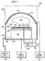
- FIG. 1depicts a conventional reactive ion etch (RIE) reactor 100 such as the decoupled plasma source (DPS) metal etch chamber that is manufactured by Applied Material, Inc. of Santa Clara, California.
- RIEreactive ion etch
- DPSdecoupled plasma source
- Such a chamberis an example of one of many types of reactive ion etch chambers that can be used with the present invention for etching photomasks upon reticles for photolithography applications.
- the DPS metal etch chamberin particular, is well suited for etching metals such as chrome that are used to form photomasks on reticles.
- the DPS chamber 100includes a vacuum chamber 112, a first RF power source 114, a second RF power source 116, a vacuum pump 118, and a top housing 126.
- the vacuum chamber 112is defined by a ceramic or quartz dome 110, a cylindrical side wall 120 and a bottom 122.
- the top housing 126generally encloses dome and wafer heating and cooling apparatus (not shown).
- the pedestal 102generally has a biased cathode 104 and an electrostatic chuck 106 for retaining wafers in the chamber 100.
- the DPS chamber 100also features a powered antenna 108 located above the wafer on the outside of a quartz dome 110.
- the vacuum chamber 100is coupled to the vacuum pump 118 to draw a vacuum inside the chamber.
- process gasese.g., Cl 2 and O 2
- process gas source 124e.g., Cl 2 and O 2
- a plasma 126is formed in the chamber to etch a semiconductor wafer, or in this case, a photomask 128 of a reticle 30.
- the pedestal 102is designed for retaining a circular (e.g., 8 inch (200 mm)) semiconductor wafer.
- a circular (e.g., 8 inch (200 mm)) semiconductor waferTo enable a square (e.g., 6 inch by 6 inch) to be etched in the DPS chamber, an adapter 132 must adapt the circular wafer support surface 134 into a square reticle support surface 136. Additionally, the adapter 132 must cover the entire surface of the electrostatic chuck 106 that is not covered by the reticle 130 such that the plasma 126 does not contact the chuck surface 134 and produce contaminants in the chamber 112 as well as destroy the electrostatic chuck 106.
- the adapter 132replaces the standard collar that generally surrounds the wafer and protects the pedestal from being etched or, in an alternative embodiment of the invention, the adapter mates with a modified collar (not shown) to accomplish the same purpose, i.e., protect the pedestal from the plasma.
- the adapter 132covers all areas of the electrostatic chuck that are not otherwise covered by the reticle or existing chamber components.
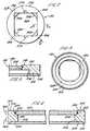
- FIGs. 2, 3 and 4respectively depict a top, bottom and cross-sectional views of the inventive reticle adapter 132. To best understand the invention the reader should refer to all these drawings simultaneously while reading the following disclosure.
- the adapter 132is generally formed from a single piece of etch resistant, high temperature resistant material such as polyimide ceramic or quartz. Such a material that withstands high temperature is manufactured by DuPont de Nemours, Inc. under the registered trademark VESPEL. A solid block or a laminate of this material can be milled into the shape of the adapter 132. Using a laminate of material layers provides certain manufacturability benefits that can be used to encapsulate a reticle retainer into the adapter, as described below with respect to FIGS.6 and 7.
- the upper portion 200 of the adapter 132contains a substantially square opening 204 that is sized to the outer shape of a reticle (shown in phantom as 130 in FIG.
- Each corner 206 of the opening 204contains a support region 208 in each corner 206 that extends into the opening 204 such that the reticle 130 rests upon the support region 208 and not fall completely through the adapter 132.
- the upper surface 210 of the adapter 132extends a slight distance above the reticle 130 when the reticle 130 is placed inside the opening 204.
- the lower portion 202 of the adapter 132is milled to have a form that conformally fits over the top of the pedestal in the RIE chamber or, alternatively, mates to a separate modified collar.
- a modified collar and adaptermay include an alignment member or key such as a protrusion on the collar and a detent to accept the protrusion on the adapter.
- the lower circular opening defined by vertical wall 216is provided with a flat 350 that matches the flat on the semiconductor wafer electrostatic chuck.
- the adapter 132can be used for orienting the reticle within the chamber such that the flat of the chuck (generally used to orient wafers) matches the flat on the adapter and the reticle will always be properly aligned in the chamber.
- the adapter 132has an overhanging vertical lip 212 (or alignment key) that extends over the outer sidewall of the pedestal, a horizontal extension 214 that rests upon the flange of the electrostatic chuck, a vertical portion 216 that extends along the vertical edge of the electrostatic chuck, and a support region 208 upon which the reticle 130 rests.
- the height of the support region 208 above the chuck surfaceinsures that the reticle 130 when resting in the adapter 132 does not contact the surface of the electrostatic chuck thus reducing the contaminants that may be transmitted from the electrostatic chuck surface to the backside of the reticle.
- the reticle and surfaceare spaced apart by about 1 mil. Such contaminants would be very hard to remove from the reticle and, if not removed, would interfere with the photolithography process.
- the reticle adapter 132can be used, as shown, as a reticle carrier such that the reticle may be carried from location to location by holding the adapter 132 and not the reticle itself. As such, fingerprints and other residue from a person's hands will not contact the reticle. Furthermore, by using the adapter 132 as a reticle carrier, the reticle carrier can be rested on a flat surface and it maintains a space between the reticle and the surface. Consequently, contaminant particles will not be "picked up" by the reticle and the reticle will not be scratched by contact with other surfaces.
- the adapter 132may be provided with a plurality access features or elements.
- such featuresare implemented as access indentations 275.
- the inventionmay have any number of access indentations 275 on one or more of the sides of opening 204.
- the indentations 275allow fingertip access to the sidewalls of the reticle 130 such that lifting the reticle from the adapter 132 is simplified. Similar access indentations could be used to provide a robot gripping mechanism with access to the sidewalls of the reticle 130.
- FIGS. 6 and 7respectively depict top and bottom cross sectional views of one embodiment of a reticle carrier 600 having a reticle retainer 602.
- the reticle retainer 602may be one of many different devices that applies a force to the reticle to retain it in the adapter.
- FIGS. 6 and 7uses a set of four retainer plates 604A-604D positioned about the perimeter of the opening 204 (i.e., one plate in each side). Each plate 604 is mounted to a pair of retaining pins 606. The pins 606 slideably engage a pair of bores 508. The head 610 of each pin 606 is retained by a barrier portion 612 located in each bore 608. A coil spring 614 circumscribes each pin 606 and has one end of the spring 614 abutting a backside of the plate 604 and the second end of the spring 614 abutting the barrier portion 612. The pin heads 610 slideably engage an outer portion of bores 608.
- the bores 608 and barrier portion 612may be fabricated with to components where the bore is drilled and an annular barrier portion 612 then affixed into each of the bores 608, or, alternatively, the bores 608 and their respective barrier portions 612 are integrally formed into the material of the carrier as the carrier is fabricated from a laminate of material.
- the pins 606can then be embedded into the carrier 600 during fabrication.
- the springs 614bias the plates 604 into contact with the reticle 130.
- the plates 604rest against the sidewalls 620 of the reticle 130 such that the plates 604 apply a force to all sides of the reticle 130 that will retain the reticle within the carrier 600.
- the reticlemay be removed from the carrier by disengaging the plates 604 from the sidewalls of the reticle, i.e., by compressing the springs and lifting the reticle from the carrier 600. While the reticle is within the carrier, the reticle may be moved from place to place, whether by robotic means or by human hands, without the robot or human touching the reticle and placing contaminants thereupon. Also, once the reticle is affixed to the carrier, a plurality of carriers can be stacked in a cassette much like wafers are transported in a cassette.
- the reticle 130may be sealed within the adapter 132 by an o-ring 300 that generally circumscribes the square opening 204.
- the o-ringis fabricated from a conventional high-temperature resilient material such as Viton or Chem-Res.
- the o-ring 300lies within a trough 302.
- the backside gasis an inert gas such as either helium or argon.
- the backside gasis optionally supplied by gas source 150 (shown in phantom in FIG. 1) through gas portals to the surface of the electrostatic chuck 106. To promote heat transfer from the reticle 130 to the chuck 106, the gas fills the space 152 between the back of the reticle 130 and the surface of the chuck 106.
- a substantial gas pressuremay exist beneath the adapter. This gas pressure may be great enough to lift the adapter from the chuck.
- the adaptercould be weighted with heavy material, e.g., lead, encapsulated in the adapter.
- a clamp ringcan be fitted to the periphery of the adapter to retain the adapter upon the chuck when substantial backside gas pressure is applied between the chuck and the reticle. Such a clamp ring would be similar to that used to retain a wafer upon a chuck in a MxP chamber of a P5000 platform, as manufactured by Applied Materials, Inc. of Santa Clara, California.
Landscapes
- Engineering & Computer Science (AREA)
- Physics & Mathematics (AREA)
- Microelectronics & Electronic Packaging (AREA)
- General Physics & Mathematics (AREA)
- Manufacturing & Machinery (AREA)
- Computer Hardware Design (AREA)
- Condensed Matter Physics & Semiconductors (AREA)
- Power Engineering (AREA)
- Plasma & Fusion (AREA)
- Chemical & Material Sciences (AREA)
- Analytical Chemistry (AREA)
- Exposure And Positioning Against Photoresist Photosensitive Materials (AREA)
- Preparing Plates And Mask In Photomechanical Process (AREA)
- Drying Of Semiconductors (AREA)
Abstract

Description
The invention generally relates to reactive ion etchingsystems for photomask fabrication upon a reticle and, moreparticularly, to a reticle adapter that facilitates dryetching a photomask using a conventional reactive ion etchchamber.
Semiconductor lithography is accomplished using areticle comprising a relatively thick substrate typicallyfabricated of quartz, having a photomask fabricated ofchrome patterned upon the surface of the substrate. Areticle is generally 5 inches by 5 inches, 6 inches by 6inches or 9 inches by 9 inches. To fabricate the photomaskpattern, a uniform submicron (e.g., 0.1 to 1.0 micron) thicklayer of chrome has a photoresist layer applied thereto.The photoresist is then patterned using conventional laseror electron beam patterning equipment. The chrome layer isthen etched using a wet etch process to remove material notprotected by the photoresist. The isotropic characteristicof a wet etch causes an undercut phenomenon to occur belowthe photoresist material such that the chrome lines that arepatterned upon the reticle are not uniformly spaced nor dothey have vertical side walls. Such undercut on photomaskpatterns that will be used to produce sub 0.25 µm devicescan result in erroneous lithography.
As semiconductor devices shrink in size, the on-maskchrome structures must also experience a correspondingreduction in size. The use of optical proximity correction(OPC) structures that are generally needed to minimize linesfor shortening and corner rounding have necessitatedsignificantly smaller features to be etched into the chrome.With the need for OPC structures and the small line widths of the chrome features, the use of wet etching to formphotomasks has become undesirable. Additionally, theenvironmental concerns for disposal of the by-products of awet etch process have also led to wet etch photomaskprocessing's undesirability.
Plasma etch processing (also known as dry etchprocessing) provides an alternative to wet etching and canprovide superior photomask fabrication results. Dry etch ofphotomasks for lithography reticles has been shown toimprove resolution, critical dimensions and criticaldimension linearity as well as take advantage of theanisotropic etch characteristics such that very little or noundercutting is experienced. Although reactive ion etchingto form photomasks has been shown to have superior resultscompared to wet etch, the industry has been slow to designnew and costly dry etch chambers and equipment to facilitatephotomask generation. Conversion of traditional waferetching equipment that is intended to handle 8 inch (200 mm)circular wafers into a system for handling 5, 6 or 9 inchsquare reticles typically requires replacement of the wafersupport pedestal. This is generally costly and complicated.
Therefore, there is a need in the art for an adapterthat can be used to convert a conventional reactive ion etchchamber into a chamber capable of dry etching a photomaskwithout substantial cost or complicated equipment.
The disadvantages associated with the prior art areovercome by the invention of a reticle adapter that iscapable of supporting a square reticle in a conventionalreactive ion etch (RIE) chamber that is designed for etchingcircular silicon wafers. In short, the adapter converts thecircular pedestal into a square photomask reticle support.The adapter is fabricated from a non-reactive material suchas polyimide, ceramic or quartz.
More specifically, the adapter has a base portion thatis milled to conformally cover the entire upper portion of a wafer pedestal such that plasma cannot contact the pedestal.The adapter contains a base portion that has a circular planform and an inner surface that follows the contours of thetop of the pedestal. The reticle rests in the upper portionof the adapter, spaced apart from the pedestal uppersurface. As such, the reticle backside will not contact thepedestal surface and become contaminated or scratched. Thereticle backside is only contacted by the adapter at itsfour corners or its edges such that the central portion ofthe reticle through which light passes during lithography isnot contacted by the adapter nor any part of the reactiveion etch chamber.
The adapter is designed to fit over the electrostaticchuck of a reactive ion etch chamber such as the decoupledplasma source (DPS) metal etch chamber fabricated by AppliedMaterials, Inc. of Santa Clara, California. Once supportedin the chamber a plasma is generated above the reticle suchthat the photomask is etched in approximately 2 minutes toremove the excess chrome that is not protected byphotoresist material and leave a photolithography patternbehind.
The reticle adapter can be also outfitted withmechanical restraining elements to hold the reticle withinthe adapter such that once the reticle is loaded into theadapter it never needs to be contacted by either robotics orhuman hands. As such, the reticle can be easily carriedfrom place to place and chamber to chamber as processing isaccomplished. One embodiment of a mechanical retainerconsists of four either spring loaded or threaded screwsthat are screwed into the sides of the adapter and can betightened to apply force to the reticle such that thereticle will not fall out of the adapter once the screws aretightened. Consequently, the invention is not only anadapter, but a reticle carrier as well.
The teachings of the present invention can be readilyunderstood by considering the following detailed descriptionin conjunction with the accompanying drawings, in which:
To facilitate understanding, identical referencenumerals have been used, where possible, to designateidentical elements that are common to the figures.
FIG. 1 depicts a conventional reactive ion etch (RIE)reactor 100 such as the decoupled plasma source (DPS) metaletch chamber that is manufactured by Applied Material, Inc.of Santa Clara, California. Such a chamber is an example ofone of many types of reactive ion etch chambers that can beused with the present invention for etching photomasks uponreticles for photolithography applications. The DPS metaletch chamber, in particular, is well suited for etchingmetals such as chrome that are used to form photomasks onreticles.
TheDPS chamber 100 includes a vacuum chamber 112, afirstRF power source 114, a secondRF power source 116, avacuum pump 118, and atop housing 126. The vacuum chamber112 is defined by a ceramic or quartz dome 110, acylindrical side wall 120 and abottom 122. Thetop housing 126 generally encloses dome and wafer heating and coolingapparatus (not shown). Thepedestal 102 generally has abiased cathode 104 and an electrostatic chuck 106 forretaining wafers in thechamber 100. TheDPS chamber 100also features a poweredantenna 108 located above the waferon the outside of a quartz dome 110. Thevacuum chamber 100is coupled to thevacuum pump 118 to draw a vacuum insidethe chamber. Once a vacuum is established, process gases(e.g., Cl2 and O2) are pumped into the chamber fromprocessgas source 124 and power supplied to both thecathode 104and theantenna 108. Aplasma 126 is formed in the chamberto etch a semiconductor wafer, or in this case, aphotomask 128 of a reticle 30.
Thepedestal 102 is designed for retaining a circular(e.g., 8 inch (200 mm)) semiconductor wafer. To enable asquare (e.g., 6 inch by 6 inch) to be etched in the DPSchamber, anadapter 132 must adapt the circularwafersupport surface 134 into a squarereticle support surface 136. Additionally, theadapter 132 must cover the entiresurface of the electrostatic chuck 106 that is not coveredby thereticle 130 such that theplasma 126 does not contactthechuck surface 134 and produce contaminants in thechamber 112 as well as destroy the electrostatic chuck 106.In one embodiment of the invention, theadapter 132 replacesthe standard collar that generally surrounds the wafer andprotects the pedestal from being etched or, in analternative embodiment of the invention, the adapter mateswith a modified collar (not shown) to accomplish the samepurpose, i.e., protect the pedestal from the plasma.Generally speaking, theadapter 132 covers all areas of theelectrostatic chuck that are not otherwise covered by thereticle or existing chamber components.
FIGs. 2, 3 and 4 respectively depict a top, bottom andcross-sectional views of theinventive reticle adapter 132.To best understand the invention the reader should refer toall these drawings simultaneously while reading thefollowing disclosure.
Theadapter 132 is generally formed from a single pieceof etch resistant, high temperature resistant material suchas polyimide ceramic or quartz. Such a material thatwithstands high temperature is manufactured by DuPont deNemours, Inc. under the registered trademark VESPEL. Asolid block or a laminate of this material can be milledinto the shape of theadapter 132. Using a laminate ofmaterial layers provides certain manufacturability benefitsthat can be used to encapsulate a reticle retainer into theadapter, as described below with respect to FIGS.6 and 7.In FIGS. 2, 3 and 4, theupper portion 200 of theadapter 132 contains a substantiallysquare opening 204 that issized to the outer shape of a reticle (shown in phantom as130 in FIG. 4), i.e., a 6 inch by 6 inch square withroundedcorners 206. Eachcorner 206 of theopening 204 contains asupport region 208 in eachcorner 206 that extends into theopening 204 such that thereticle 130 rests upon thesupportregion 208 and not fall completely through theadapter 132.Theupper surface 210 of theadapter 132 extends a slightdistance above thereticle 130 when thereticle 130 isplaced inside theopening 204. Thelower portion 202 of theadapter 132 is milled to have a form that conformally fitsover the top of the pedestal in the RIE chamber or,alternatively, mates to a separate modified collar.
To facilitate reticle alignment, a modified collar andadapter may include an alignment member or key such as aprotrusion on the collar and a detent to accept theprotrusion on the adapter. Alternatively, as shown inphantom in FIG. 3, the lower circular opening defined byvertical wall 216 is provided with a flat 350 that matchesthe flat on the semiconductor wafer electrostatic chuck. Assuch, theadapter 132 can be used for orienting the reticlewithin the chamber such that the flat of the chuck(generally used to orient wafers) matches the flat on theadapter and the reticle will always be properly aligned inthe chamber.
To fit the DPS chamber, for example, theadapter 132has an overhanging vertical lip 212 (or alignment key) that extends over the outer sidewall of the pedestal, ahorizontal extension 214 that rests upon the flange of theelectrostatic chuck, avertical portion 216 that extendsalong the vertical edge of the electrostatic chuck, and asupport region 208 upon which thereticle 130 rests. Theheight of thesupport region 208 above the chuck surfaceinsures that thereticle 130 when resting in theadapter 132does not contact the surface of the electrostatic chuck thusreducing the contaminants that may be transmitted from theelectrostatic chuck surface to the backside of the reticle.The reticle and surface are spaced apart by about 1 mil.Such contaminants would be very hard to remove from thereticle and, if not removed, would interfere with thephotolithography process.
Thereticle adapter 132 can be used, as shown, as areticle carrier such that the reticle may be carried fromlocation to location by holding theadapter 132 and not thereticle itself. As such, fingerprints and other residuefrom a person's hands will not contact the reticle.Furthermore, by using theadapter 132 as a reticle carrier,the reticle carrier can be rested on a flat surface and itmaintains a space between the reticle and the surface.Consequently, contaminant particles will not be "picked up"by the reticle and the reticle will not be scratched bycontact with other surfaces.
To facilitate easy loading and removal of thereticle 130 to/from theadapter 132 without touching the glasssurfaces of the reticle, theadapter 132 may be providedwith a plurality access features or elements. In theembodiment shown, such features are implemented asaccessindentations 275. Although only twoindentations 275 areshown, the invention may have any number ofaccessindentations 275 on one or more of the sides ofopening 204.Theindentations 275 allow fingertip access to the sidewallsof thereticle 130 such that lifting the reticle from theadapter 132 is simplified. Similar access indentationscould be used to provide a robot gripping mechanism withaccess to the sidewalls of thereticle 130.
To improve the adapter's function as a reticle carrierand insure that the reticle will not fall out of the adapterand become broken, a mechanical retaining apparatus may beprovided to insure that the reticle remains within theadapter. FIGS. 6 and 7 respectively depict top and bottomcross sectional views of one embodiment of areticle carrier 600 having a reticle retainer 602. The reticle retainer 602may be one of many different devices that applies a force tothe reticle to retain it in the adapter.
The illustrative embodiment of FIGS. 6 and 7 uses a setof four retainer plates 604A-604D positioned about theperimeter of the opening 204 (i.e., one plate in each side).Each plate 604 is mounted to a pair of retaining pins 606.Thepins 606 slideably engage a pair ofbores 508. Thehead 610 of eachpin 606 is retained by abarrier portion 612located in eachbore 608. Acoil spring 614 circumscribeseachpin 606 and has one end of thespring 614 abutting abackside of the plate 604 and the second end of thespring 614 abutting thebarrier portion 612. The pin heads 610slideably engage an outer portion ofbores 608. Thebores 608 andbarrier portion 612 may be fabricated with tocomponents where the bore is drilled and anannular barrierportion 612 then affixed into each of thebores 608, or,alternatively, thebores 608 and theirrespective barrierportions 612 are integrally formed into the material of thecarrier as the carrier is fabricated from a laminate ofmaterial. Thepins 606 can then be embedded into thecarrier 600 during fabrication.
Thesprings 614 bias the plates 604 into contact withthereticle 130. The plates 604 rest against the sidewalls620 of thereticle 130 such that the plates 604 apply aforce to all sides of thereticle 130 that will retain thereticle within thecarrier 600.
The reticle may be removed from the carrier bydisengaging the plates 604 from the sidewalls of thereticle, i.e., by compressing the springs and lifting thereticle from thecarrier 600. While the reticle is withinthe carrier, the reticle may be moved from place to place, whether by robotic means or by human hands, without therobot or human touching the reticle and placing contaminantsthereupon. Also, once the reticle is affixed to thecarrier, a plurality of carriers can be stacked in acassette much like wafers are transported in a cassette.
Alternatively, as depicted in phantom in FIG. 5, thereticle 130 may be sealed within theadapter 132 by an o-ring 300 that generally circumscribes thesquare opening 204. The o-ring is fabricated from a conventional high-temperatureresilient material such as Viton or Chem-Res.The o-ring 300 lies within atrough 302. When areticle 130is inserted into theopening 204, the o-ring is compressedand applies pressure or force upon the outside perimeter ofthereticle 130 and thereby forms another embodiment of areticle retainer that holds thereticle 130 in theadapter 132. Using an o-ring 300 to seal thereticle 130 to theadapter 132 also enables "backside gas" to be appliedbetween the reticle and the pedestal surface such that heatwill conduct from the reticle to the pedestal. Generally,the backside gas is an inert gas such as either helium orargon. The backside gas is optionally supplied by gassource 150 (shown in phantom in FIG. 1) through gas portalsto the surface of the electrostatic chuck 106. To promoteheat transfer from thereticle 130 to the chuck 106, the gasfills thespace 152 between the back of thereticle 130 andthe surface of the chuck 106.
To sufficiently transfer heat from the reticle to thechuck, a substantial gas pressure may exist beneath theadapter. This gas pressure may be great enough to lift theadapter from the chuck. To compensate for the gas pressure,the adapter could be weighted with heavy material, e.g.,lead, encapsulated in the adapter. Alternatively, a clampring can be fitted to the periphery of the adapter to retainthe adapter upon the chuck when substantial backside gaspressure is applied between the chuck and the reticle. Sucha clamp ring would be similar to that used to retain a waferupon a chuck in a MxP chamber of a P5000 platform, as manufactured by Applied Materials, Inc. of Santa Clara,California.
Although various embodiments which incorporate theteachings of the present invention have been shown anddescribed in detail herein, those skilled in the art canreadily devise many other varied embodiments that stillincorporate these teachings.
Claims (22)
- Apparatus for supporting a photolithography reticle in asemiconductor wafer processing system comprising:an adapter having first portion on a first side thatmatches the size and shape of a pedestal and a secondportion on a second side that matches the size and shape ofa photolithography reticle.
- The apparatus of claim 1 wherein said first portiondefines a first opening.
- The apparatus of claim 1 wherein said second portiondefines a second opening.
- The apparatus of claim 2 wherein the first opening isadapted to rest upon a pedestal of a reactive ion etch (RIE)chamber.
- The apparatus of claim 3 wherein the second opening isadapted for supporting a reticle during photomask etchingprocesses.
- The apparatus of claim 3 further comprising a pluralityof reticle support members located within the secondopening.
- The apparatus of claim 6 wherein the second opening issubstantially square having four corners and the reticlesupport members are located in each corner.
- The apparatus of claim 3 further comprising a reticleretainer located within the second opening.
- The apparatus of claim 8 wherein said reticle retainercomprises:at least one plate, having a longitudinal axis parallelwith an edge of said second opening, where said at least oneplate extends from said peripheral edge of said secondopening into said second opening.
- The apparatus of claim 9 wherein said reticle retainerfurther comprises:at least one resilient member for biasing the at leastone plate into the second opening.
- The apparatus of claim 8 wherein said reticle retainercomprises:four plates, where each plate has a longitudinal axisaligned with an edge of the second opening;at least one spring for each plate, disposed betweeneach plate and an edge of said second opening to bias eachof said four plates into said second opening.
- The apparatus of claim 3 wherein said second opening iscircumscribed by an O-ring.
- A reactive ion etch chamber comprising:a pedestal having a support surface; andan adapter having a first side that covers said supportsurface of said pedestal and a second side to support aphotolithography reticle within the chamber.
- The reactive ion etch chamber of claim 13 wherein saidfirst side and said second side are separated by a supportregion that supports paid reticle in a spaced apart relationwith respect to the circular support surface to form a spacetherebetween.
- The reactive ion etch chamber of claim 14 wherein saidsecond side further comprises a seal between said reticleand said second side.
- The reactive ion etch chamber of claim 15 wherein saidseal retains a gas within said space between said reticleand said support surface.
- The reactive ion etch chamber of claim 16 wherein saidseal is an 0-ring that is located in a channel thatcircumscribes an opening within which the reticle resides.
- A reticle carrier comprising:a carrier body having an opening sized and shaped toaccept a reticle; anda reticle retainer positioned within said opening.
- The apparatus of claim 18 wherein said reticle retainercomprises:at least one plate, having a longitudinal axis parallelwith an edge of said opening, where said at least one plateextends from said peripheral edge of said opening into saidsecond opening.
- The apparatus of claim 19 wherein said reticle retainerfurther comprises:at least one resilient member for biasing the at leastone plate into the second opening.
- The apparatus of claim 18 wherein said reticle retainercomprises:four plates, where each plate has a longitudinal axisaligned with an edge of the opening;at least one spring for each plate, disposed betweeneach plate and an edge of said opening to bias each of saidfour plates into said opening.
- The apparatus of claim 18 wherein said reticle retaineris an O-ring that circumscribes said opening.
Applications Claiming Priority (2)
| Application Number | Priority Date | Filing Date | Title |
|---|---|---|---|
| US238205 | 1999-01-27 | ||
| US09/238,205US6251217B1 (en) | 1999-01-27 | 1999-01-27 | Reticle adapter for a reactive ion etch system |
Publications (2)
| Publication Number | Publication Date |
|---|---|
| EP1024520A2true EP1024520A2 (en) | 2000-08-02 |
| EP1024520A3 EP1024520A3 (en) | 2003-11-12 |
Family
ID=22896920
Family Applications (1)
| Application Number | Title | Priority Date | Filing Date |
|---|---|---|---|
| EP00300502AWithdrawnEP1024520A3 (en) | 1999-01-27 | 2000-01-24 | Reticle adapter for a reactive ion etch system |
Country Status (5)
| Country | Link |
|---|---|
| US (2) | US6251217B1 (en) |
| EP (1) | EP1024520A3 (en) |
| JP (1) | JP2000286250A (en) |
| KR (1) | KR20000053631A (en) |
| TW (1) | TW480623B (en) |
Cited By (5)
| Publication number | Priority date | Publication date | Assignee | Title |
|---|---|---|---|---|
| US6251217B1 (en)* | 1999-01-27 | 2001-06-26 | Applied Materials, Inc. | Reticle adapter for a reactive ion etch system |
| EP1612840A3 (en)* | 2004-06-30 | 2007-07-25 | Applied Materials, Inc. | Method and apparatus for photomask plasma etching |
| US7909961B2 (en) | 2006-10-30 | 2011-03-22 | Applied Materials, Inc. | Method and apparatus for photomask plasma etching |
| US7943005B2 (en) | 2006-10-30 | 2011-05-17 | Applied Materials, Inc. | Method and apparatus for photomask plasma etching |
| US8349128B2 (en) | 2004-06-30 | 2013-01-08 | Applied Materials, Inc. | Method and apparatus for stable plasma processing |
Families Citing this family (28)
| Publication number | Priority date | Publication date | Assignee | Title |
|---|---|---|---|---|
| US20030003374A1 (en)* | 2001-06-15 | 2003-01-02 | Applied Materials, Inc. | Etch process for photolithographic reticle manufacturing with improved etch bias |
| TW558861B (en)* | 2001-06-15 | 2003-10-21 | Semiconductor Energy Lab | Laser irradiation stage, laser irradiation optical system, laser irradiation apparatus, laser irradiation method, and method of manufacturing semiconductor device |
| US7183201B2 (en) | 2001-07-23 | 2007-02-27 | Applied Materials, Inc. | Selective etching of organosilicate films over silicon oxide stop etch layers |
| WO2003021659A1 (en) | 2001-09-04 | 2003-03-13 | Applied Materials, Inc. | Methods and apparatus for etching metal layers on substrates |
| WO2003089990A2 (en)* | 2002-04-19 | 2003-10-30 | Applied Materials, Inc. | Process for etching photomasks |
| US20030217693A1 (en)* | 2002-05-22 | 2003-11-27 | Applied Materials, Inc. | Substrate support assembly having an edge protector |
| US20030219986A1 (en)* | 2002-05-22 | 2003-11-27 | Applied Materials, Inc. | Substrate carrier for processing substrates |
| US6960413B2 (en)* | 2003-03-21 | 2005-11-01 | Applied Materials, Inc. | Multi-step process for etching photomasks |
| US7077973B2 (en)* | 2003-04-18 | 2006-07-18 | Applied Materials, Inc. | Methods for substrate orientation |
| US20040219790A1 (en)* | 2003-04-30 | 2004-11-04 | Wilson Aaron R | Etching methods, RIE methods, and methods of increasing the stability of photoresist during RIE |
| US7521000B2 (en)* | 2003-08-28 | 2009-04-21 | Applied Materials, Inc. | Process for etching photomasks |
| US6794662B1 (en) | 2003-10-07 | 2004-09-21 | Ibis Technology Corporation | Thermosetting resin wafer-holding pin |
| JP2005123292A (en)* | 2003-10-15 | 2005-05-12 | Canon Inc | Storage device and exposure method using the storage device |
| US7879510B2 (en) | 2005-01-08 | 2011-02-01 | Applied Materials, Inc. | Method for quartz photomask plasma etching |
| US7790334B2 (en) | 2005-01-27 | 2010-09-07 | Applied Materials, Inc. | Method for photomask plasma etching using a protected mask |
| US7829243B2 (en) | 2005-01-27 | 2010-11-09 | Applied Materials, Inc. | Method for plasma etching a chromium layer suitable for photomask fabrication |
| US7829471B2 (en)* | 2005-07-29 | 2010-11-09 | Applied Materials, Inc. | Cluster tool and method for process integration in manufacturing of a photomask |
| US20070031609A1 (en) | 2005-07-29 | 2007-02-08 | Ajay Kumar | Chemical vapor deposition chamber with dual frequency bias and method for manufacturing a photomask using the same |
| US20070217119A1 (en)* | 2006-03-17 | 2007-09-20 | David Johnson | Apparatus and Method for Carrying Substrates |
| JP2007311540A (en)* | 2006-05-18 | 2007-11-29 | Renesas Technology Corp | Method of manufacturing semiconductor device |
| EP1926125B1 (en) | 2006-10-30 | 2011-02-16 | Applied Materials, Inc. | Endpoint detection for photomask etching |
| KR100944846B1 (en)* | 2006-10-30 | 2010-03-04 | 어플라이드 머티어리얼스, 인코포레이티드 | Mask etching process |
| US7786019B2 (en) | 2006-12-18 | 2010-08-31 | Applied Materials, Inc. | Multi-step photomask etching with chlorine for uniformity control |
| US8483248B2 (en)* | 2010-09-14 | 2013-07-09 | Raytheon Company | Laser crystal components joined with thermal management devices |
| US10739671B2 (en)* | 2017-11-10 | 2020-08-11 | Taiwan Semiconductor Manufacturing Co., Ltd. | Method of manufacturing phase shift photo masks |
| US11099478B2 (en)* | 2018-08-14 | 2021-08-24 | Taiwan Semiconductor Manufacturing Co., Ltd. | Photomask having recessed region |
| GB2584160A (en)* | 2019-05-24 | 2020-11-25 | Edwards Ltd | Vacuum assembly and vacuum pump with an axial through passage |
| US11014732B2 (en)* | 2019-06-21 | 2021-05-25 | Universal Trim Supply Co., Ltd. | Vacuum storage bag assembly and vacuum storage system therewith |
Family Cites Families (12)
| Publication number | Priority date | Publication date | Assignee | Title |
|---|---|---|---|---|
| US3207126A (en)* | 1961-11-14 | 1965-09-21 | Byron Ernest | Mask changer means for vacuum deposition device |
| US4926489A (en)* | 1983-03-11 | 1990-05-15 | Kla Instruments Corporation | Reticle inspection system |
| US4889998A (en)* | 1987-01-29 | 1989-12-26 | Nikon Corporation | Apparatus with four light detectors for checking surface of mask with pellicle |
| JPH06232236A (en)* | 1991-08-20 | 1994-08-19 | Fujitsu Ltd | Manufacture of semiconductor device |
| JPH06120131A (en)* | 1992-10-08 | 1994-04-28 | Sumitomo Electric Ind Ltd | Wafer adapter |
| JPH09148219A (en)* | 1995-11-21 | 1997-06-06 | Nikon Corp | Board adapter |
| JP3689949B2 (en)* | 1995-12-19 | 2005-08-31 | 株式会社ニコン | Projection exposure apparatus and pattern forming method using the projection exposure apparatus |
| US5805408A (en)* | 1995-12-22 | 1998-09-08 | Lam Research Corporation | Electrostatic clamp with lip seal for clamping substrates |
| US5750003A (en)* | 1996-05-20 | 1998-05-12 | Taiwan Semiconductor Manufacturing Company, Ltd. | Chuck for holding semiconductor photolithography masks |
| US6530994B1 (en)* | 1997-08-15 | 2003-03-11 | Micro C Technologies, Inc. | Platform for supporting a semiconductor substrate and method of supporting a substrate during rapid high temperature processing |
| US6251217B1 (en)* | 1999-01-27 | 2001-06-26 | Applied Materials, Inc. | Reticle adapter for a reactive ion etch system |
| US6232247B1 (en)* | 1999-09-01 | 2001-05-15 | Micron Technology, Inc. | Substrate coating apparatus and semiconductor processing method of improving uniformity of liquid deposition |
- 1999
- 1999-01-27USUS09/238,205patent/US6251217B1/ennot_activeExpired - Lifetime
- 2000
- 2000-01-19TWTW089100845Apatent/TW480623B/ennot_activeIP Right Cessation
- 2000-01-24EPEP00300502Apatent/EP1024520A3/ennot_activeWithdrawn
- 2000-01-27JPJP2000057861Apatent/JP2000286250A/ennot_activeWithdrawn
- 2000-01-27KRKR1020000003921Apatent/KR20000053631A/ennot_activeWithdrawn
- 2001
- 2001-05-29USUS09/866,883patent/US6607634B2/ennot_activeExpired - Fee Related
Cited By (8)
| Publication number | Priority date | Publication date | Assignee | Title |
|---|---|---|---|---|
| US6251217B1 (en)* | 1999-01-27 | 2001-06-26 | Applied Materials, Inc. | Reticle adapter for a reactive ion etch system |
| US6607634B2 (en)* | 1999-01-27 | 2003-08-19 | Applied Materials, Inc. | Reticle adapter for a reactive ion etch system |
| EP1612840A3 (en)* | 2004-06-30 | 2007-07-25 | Applied Materials, Inc. | Method and apparatus for photomask plasma etching |
| US8349128B2 (en) | 2004-06-30 | 2013-01-08 | Applied Materials, Inc. | Method and apparatus for stable plasma processing |
| US8801896B2 (en) | 2004-06-30 | 2014-08-12 | Applied Materials, Inc. | Method and apparatus for stable plasma processing |
| US7909961B2 (en) | 2006-10-30 | 2011-03-22 | Applied Materials, Inc. | Method and apparatus for photomask plasma etching |
| US7943005B2 (en) | 2006-10-30 | 2011-05-17 | Applied Materials, Inc. | Method and apparatus for photomask plasma etching |
| US8568553B2 (en) | 2006-10-30 | 2013-10-29 | Applied Materials, Inc. | Method and apparatus for photomask plasma etching |
Also Published As
| Publication number | Publication date |
|---|---|
| TW480623B (en) | 2002-03-21 |
| US20010022216A1 (en) | 2001-09-20 |
| US6251217B1 (en) | 2001-06-26 |
| EP1024520A3 (en) | 2003-11-12 |
| JP2000286250A (en) | 2000-10-13 |
| US6607634B2 (en) | 2003-08-19 |
| KR20000053631A (en) | 2000-08-25 |
Similar Documents
| Publication | Publication Date | Title |
|---|---|---|
| US6251217B1 (en) | Reticle adapter for a reactive ion etch system | |
| US7128806B2 (en) | Mask etch processing apparatus | |
| JP4869533B2 (en) | Apparatus for supporting process chamber and substrate | |
| US7160392B2 (en) | Method for dechucking a substrate | |
| US6927842B2 (en) | Wafer handling method for use in lithography patterning | |
| US6513796B2 (en) | Wafer chuck having a removable insert | |
| EP2831673B1 (en) | Apparatus and methods for reticle handling in an euv reticle inspection tool | |
| US20050152088A1 (en) | Substrate holding system and exposure apparatus using the same | |
| WO2005064670A1 (en) | A pedestal for an etch processing apparatus | |
| US6900878B2 (en) | Reticle-holding pods and methods for holding thin, circular reticles, and reticle-handling systems utilizing same | |
| US7065894B2 (en) | Apparatus for kinematic registration of a reticle | |
| US20030219986A1 (en) | Substrate carrier for processing substrates | |
| US20030217693A1 (en) | Substrate support assembly having an edge protector | |
| JP4518712B2 (en) | Tray-type multi-chamber substrate processing equipment | |
| JP7702627B2 (en) | Plasma processing apparatus and plasma processing method | |
| US20050133158A1 (en) | Mask handler apparatus | |
| JP2009105238A (en) | Substrate holder, exposure apparatus, device manufacturing method and substrate transport method. | |
| JP2000100914A (en) | Substrate suction device and exposure device |
Legal Events
| Date | Code | Title | Description |
|---|---|---|---|
| PUAI | Public reference made under article 153(3) epc to a published international application that has entered the european phase | Free format text:ORIGINAL CODE: 0009012 | |
| AK | Designated contracting states | Kind code of ref document:A2 Designated state(s):AT BE CH CY DE DK ES FI FR GB GR IE IT LI LU MC NL PT SE | |
| AX | Request for extension of the european patent | Free format text:AL;LT;LV;MK;RO;SI | |
| PUAL | Search report despatched | Free format text:ORIGINAL CODE: 0009013 | |
| AK | Designated contracting states | Kind code of ref document:A3 Designated state(s):AT BE CH CY DE DK ES FI FR GB GR IE IT LI LU MC NL PT SE | |
| AX | Request for extension of the european patent | Extension state:AL LT LV MK RO SI | |
| 17P | Request for examination filed | Effective date:20040511 | |
| AKX | Designation fees paid | Designated state(s):DE GB NL | |
| 17Q | First examination report despatched | Effective date:20040927 | |
| STAA | Information on the status of an ep patent application or granted ep patent | Free format text:STATUS: THE APPLICATION IS DEEMED TO BE WITHDRAWN | |
| 18D | Application deemed to be withdrawn | Effective date:20050209 |