EP1020900A2 - Semiconductor device and method for fabricating the same - Google Patents
Semiconductor device and method for fabricating the sameDownload PDFInfo
- Publication number
- EP1020900A2 EP1020900A2EP00100592AEP00100592AEP1020900A2EP 1020900 A2EP1020900 A2EP 1020900A2EP 00100592 AEP00100592 AEP 00100592AEP 00100592 AEP00100592 AEP 00100592AEP 1020900 A2EP1020900 A2EP 1020900A2
- Authority
- EP
- European Patent Office
- Prior art keywords
- layer
- semiconductor
- gate electrode
- channel
- inhibitor
- Prior art date
- Legal status (The legal status is an assumption and is not a legal conclusion. Google has not performed a legal analysis and makes no representation as to the accuracy of the status listed.)
- Granted
Links
Images


Classifications
- H—ELECTRICITY
- H01—ELECTRIC ELEMENTS
- H01L—SEMICONDUCTOR DEVICES NOT COVERED BY CLASS H10
- H01L21/00—Processes or apparatus adapted for the manufacture or treatment of semiconductor or solid state devices or of parts thereof
- H01L21/02—Manufacture or treatment of semiconductor devices or of parts thereof
- H01L21/04—Manufacture or treatment of semiconductor devices or of parts thereof the devices having potential barriers, e.g. a PN junction, depletion layer or carrier concentration layer
- H01L21/18—Manufacture or treatment of semiconductor devices or of parts thereof the devices having potential barriers, e.g. a PN junction, depletion layer or carrier concentration layer the devices having semiconductor bodies comprising elements of Group IV of the Periodic Table or AIIIBV compounds with or without impurities, e.g. doping materials
- H01L21/26—Bombardment with radiation
- H01L21/263—Bombardment with radiation with high-energy radiation
- H01L21/265—Bombardment with radiation with high-energy radiation producing ion implantation
- H01L21/26506—Bombardment with radiation with high-energy radiation producing ion implantation in group IV semiconductors
- H—ELECTRICITY
- H10—SEMICONDUCTOR DEVICES; ELECTRIC SOLID-STATE DEVICES NOT OTHERWISE PROVIDED FOR
- H10D—INORGANIC ELECTRIC SEMICONDUCTOR DEVICES
- H10D10/00—Bipolar junction transistors [BJT]
- H10D10/80—Heterojunction BJTs
- H—ELECTRICITY
- H01—ELECTRIC ELEMENTS
- H01L—SEMICONDUCTOR DEVICES NOT COVERED BY CLASS H10
- H01L21/00—Processes or apparatus adapted for the manufacture or treatment of semiconductor or solid state devices or of parts thereof
- H01L21/02—Manufacture or treatment of semiconductor devices or of parts thereof
- H01L21/04—Manufacture or treatment of semiconductor devices or of parts thereof the devices having potential barriers, e.g. a PN junction, depletion layer or carrier concentration layer
- H01L21/18—Manufacture or treatment of semiconductor devices or of parts thereof the devices having potential barriers, e.g. a PN junction, depletion layer or carrier concentration layer the devices having semiconductor bodies comprising elements of Group IV of the Periodic Table or AIIIBV compounds with or without impurities, e.g. doping materials
- H01L21/26—Bombardment with radiation
- H01L21/263—Bombardment with radiation with high-energy radiation
- H01L21/265—Bombardment with radiation with high-energy radiation producing ion implantation
- H01L21/2658—Bombardment with radiation with high-energy radiation producing ion implantation of a molecular ion, e.g. decaborane
- H—ELECTRICITY
- H10—SEMICONDUCTOR DEVICES; ELECTRIC SOLID-STATE DEVICES NOT OTHERWISE PROVIDED FOR
- H10D—INORGANIC ELECTRIC SEMICONDUCTOR DEVICES
- H10D30/00—Field-effect transistors [FET]
- H10D30/60—Insulated-gate field-effect transistors [IGFET]
- H—ELECTRICITY
- H10—SEMICONDUCTOR DEVICES; ELECTRIC SOLID-STATE DEVICES NOT OTHERWISE PROVIDED FOR
- H10D—INORGANIC ELECTRIC SEMICONDUCTOR DEVICES
- H10D30/00—Field-effect transistors [FET]
- H10D30/60—Insulated-gate field-effect transistors [IGFET]
- H10D30/751—Insulated-gate field-effect transistors [IGFET] having composition variations in the channel regions
- H—ELECTRICITY
- H10—SEMICONDUCTOR DEVICES; ELECTRIC SOLID-STATE DEVICES NOT OTHERWISE PROVIDED FOR
- H10D—INORGANIC ELECTRIC SEMICONDUCTOR DEVICES
- H10D62/00—Semiconductor bodies, or regions thereof, of devices having potential barriers
- H10D62/80—Semiconductor bodies, or regions thereof, of devices having potential barriers characterised by the materials
- H10D62/82—Heterojunctions
- H10D62/822—Heterojunctions comprising only Group IV materials heterojunctions, e.g. Si/Ge heterojunctions
- H—ELECTRICITY
- H10—SEMICONDUCTOR DEVICES; ELECTRIC SOLID-STATE DEVICES NOT OTHERWISE PROVIDED FOR
- H10D—INORGANIC ELECTRIC SEMICONDUCTOR DEVICES
- H10D62/00—Semiconductor bodies, or regions thereof, of devices having potential barriers
- H10D62/80—Semiconductor bodies, or regions thereof, of devices having potential barriers characterised by the materials
- H10D62/83—Semiconductor bodies, or regions thereof, of devices having potential barriers characterised by the materials being Group IV materials, e.g. B-doped Si or undoped Ge
- H10D62/834—Semiconductor bodies, or regions thereof, of devices having potential barriers characterised by the materials being Group IV materials, e.g. B-doped Si or undoped Ge further characterised by the dopants
Definitions
- the present inventionrelates to a semiconductor device functioning as a field effect transistor including a heterojunction and a method for fabricating the same.
- Radio frequency (RF) semiconductor deviceshave heretofore been fabricated using a substrate made of a compound semiconductor like GaAs. Recently, however, technology of fabricating RF semiconductor devices using a novel mixed crystal semiconductor, which is much more compatible with a silicon process, has been researched and developed.
- silicon germaniumwhich is expressed by a chemical formula Si 1-x Ge x (where x is a mole fraction of Ge), is highly compatible with a silicon process in view of the fabrication technology applicable thereto.
- Si 1-x Ge xis used, then it is possible to take full advantage of richly cultivated silicon processing technology.
- SiGe and silicon (Si)together form a heterojunction therebetween.
- any devicecan be designed freely. Furthermore, carriers can move at a higher mobility in an SiGe layer than in an Si layer. Accordingly, a semiconductor device including an SiGe layer can operate faster with reduced noise. Paying special attention to the advantages of SiGe such as these, bipolar transistors and field effect transistors with an Si/SiGe heterojunction have been proposed, modeled and used practically.
- HMOS transistorheterojunction MOS transistor
- SiGe layeras disclosed in Japanese Laid-Open Publication No. 3-3366.
- HMOS transistor of Solomon et al.will be labeled as first prior art example for convenience sake.
- Figure 13(a)is a cross-sectional view illustrating a structure of such an HMOS transistor according to the first prior art example.
- Figure 13(b)is a cross-sectional view illustrating the region R50a shown in Figure 13(a) .
- Figure 13(c)is a cross-sectional view illustrating movement, diffusion and segregation of Ge atoms after the HMOS transistor of the first prior art example, including a thin Si cap layer, has been annealed.
- Figure 13(d)is a cross-sectional view illustrating movement, diffusion and segregation of Ge atoms after the HMOS transistor of the first prior art example, including a thick Si cap layer, has been annealed. Only the region R50b shown in Figure 13(b) is illustrated in Figures 13(c) and 13(d) .
- the HMOS transistorincludes: Si substrate 501 ; p + -type polysilicon gate electrode 516 ; SiO 2 layer 517 ; intrinsic (i-) Si 1-y Ge y layer 519 (where y is a mole fraction of Ge); i-Si cap layer 542 ; source contact 551 connected to a source region 553 ; and drain contact 552 connected to a drain region 554 .
- the SiO 2 /Si and Si/Si 1-y Ge y interfacesare identified by the reference numerals 535 and 536 , respectively.
- the HMOS transistor shown in Figures 13(a) through 13(c)is a p-channel MOS transistor.
- the source/drain regions 553 and 554 and the gate electrode 516 thereofare in similar shapes to those of an ordinary Si MOS transistor.
- the p-channelis formed within Si 1-y Ge y layer 519 to further increase the conductivity thereof.
- the atomic radius of Ge atoms 506is greater than that of Si atoms.
- the i-Si 1-y Ge y layer 519receives a compressive strain because there is a lattice misfit between the i-Si 1-y Ge y layer 519 and the Si substrate 501 .
- a phenomenon relaxing compressive strainis likely to occur during an epitaxy.
- the Si/Si 1-y Ge y heterojunction deviceis applicable as a heterojunction PMOSFET.
- the polarity of the regions surrounding the Si/Si 1-y Ge y interface 536is inverted, thus forming a p-channel, where positive carriers (holes) are confined, along the Si/Si 1-y Ge y interface 536 .
- those carrierstravel at a high velocity from the source region 553 toward the drain region 554 .
- the Si/Si 1-y Ge y interface 536is planar, then the p-channel is formed along the planar Si/Si 1-y Ge y interface 536 , and therefore, the carriers can move at an even higher velocity.
- a field effect transistor using SiGecan operate faster than a field effect transistor using Si.
- Figure 14(a)is a cross-sectional view illustrating a semiconductor device according to the second prior art example.
- Figure 14(b)illustrates a vertical cross section of a region including gate electrode, gate insulating film and channel in the PMOS 530 or NMOS transistor 531 shown in Figure 14(a) .
- a valence bandcorresponding to a negative gate bias voltage applied.
- a conduction bandcorresponding to a positive gate bias voltage applied.
- Figure 14(c)is a cross-sectional view of the region R60b shown in Figure 14(b) illustrating movement and segregation of Ge atoms after the HCMOS transistor of the second prior art example has been annealed.
- the HCMOS transistorincludes Si substrate 501 , PMOSFET 530 , NMOSFET 531 , n-well 532 and shallow trench isolation (STI) region 534 .
- STIshallow trench isolation
- Si 1-x Ge x buffer layer 523 , i-Si 1-x Ge x spacer layer 521 , ⁇ -doped layer 522 , i-Si layer 520 , i-Si 1-y Ge y layer 519 , i-Si layer 518 , SiO 2 layer 517 and polysilicon gate electrode 516are stacked in this order.
- first, second and third interfacesare identified by the reference numerals 537 , 538 and 539 , respectively.
- an HCMOS deviceis made up of n- and p-channel field effect transistors each including the Si 1-y Ge y layer 519 .
- superior conductivityis attainable compared to a homojunction transistor formed on an Si substrate.
- the n- and p-channel MOS transistorsare formed using a common multilayer structure, the fabrication process thereof is simpler.
- the ⁇ -doped layer 522 for supplying carriers to the n-channelis defined within the i-Si 1-x Ge x spacer layer 521 .
- the i-Si layer 520 to which a tensile strain is applied, the i-Si 1-y Ge y layer 519 of which the strain has been relaxed, and the i-Si cap layer 518 to which a tensile strain is applied,are stacked one upon the other on the i-Si 1-x Ge x spacer layer 521 .
- the SiO 2 layer 517 as the gate oxide film and the gate electrode 516are formed in this order.
- a valence bandappearing when a negative gate bias voltage is applied to the multi-layered transistor shown in the center of Figure 14(b) to make the transistor operate as PMOSFET.
- a conduction bandappearing when a positive gate bias voltage is applied to the multi-layered transistor to make the transistor operate as NMOSFET. That is to say, one of the transistors can operate as PMOSFET and the other as NMOSFET by using the same multilayer structure.
- the band degeneracy of the electronshas been eliminated and the conductivity of the electrons is higher than that of electrons located within a normal channel in the Si layer.
- the magnitude of the strainis adjusted in the same way as the PMOSFET, then the band offset is also controllable.
- the same multilayer structure shown in the center of Figure 14(b)can be selectively used as NMOSFET or PMOSFET by changing the direction of the gate bias voltage. Accordingly, an HCMOS device with excellent conductivity can be obtained through relatively simple process steps if a single multilayer structure is separated and isolated via the STI to define separate source/drain regions and gate electrode.
- the interface statesgreatly affect the mobility of the carriers, and the operating speed of the device. That is to say, to make the device operate at high speeds, the structure of the Si/Si 1-y Ge y interface 536 should not be out of order, i.e., the interface thereof should be definitely defined and planar without any fluctuations or unevenness.
- the i-Si 1-y Ge y layer 519 and i-Si cap layer 542are illustrated as being clearly divided layers for the illustrative purposes only. Actually, though, the boundary between these layers 519 and 542 , i.e., the interface 536 , is not so definite as the illustrated one.
- a fabrication process of a semiconductor devicesuch as a field effect transistor
- dopantsjust after dopants have been introduced by ion implantation, for example, to define p- and n-type doped regions, those dopants are not located at crystal lattice sites.
- annealingis conducted at an elevated temperature, thereby activating the dopants. In this case, annealing is carried out at a temperature as high as about 900°C.
- the Ge atoms 506 in the i-Si 1-y Ge y layer 519move and diffuse particularly actively.
- Figures 13(c) and 13(d)are cross-sectional views illustrating post-annealing states of the region R50b shown in Figure 13(b) where the thicknesses of the i-Si cap layer 542 are relatively small and large, respectively.
- the Ge atoms 506move and diffuse to cause segregation or lattice defects and the definiteness and planarity of the Si/Si 1-y Ge y interface 536 are lost as disclosed by F. K. LeGoues, S. S. Iyer, K. N. Tu and S. L. Delage in Mat. Res. Soc. Symp. Proc., Vol. 103, 185 (1988).
- the movement, diffusion and segregation of the Ge atomsare particularly noticeable in an SiGe layer to which some strain is applied.
- the SiO 2 layer 517is formed as the gate oxide film by thermal oxidation.
- the Ge atomsare segregated at the Si/SiO 2 interface 535 and increase the oxidation rate as disclosed by G. L. Patton, S. S. Iyer, S. L. Delage, E. Ganin and R. C. Mcintosh in Mat. Res. Soc. Symp. Proc., Vol. 102, 295 (1988).
- Such a phenomenonis believed to cause various adverse effects.
- the interface level of the Si/SiO 2 interface 535rises, thus adversely affecting the mobility of carriers moving in the p-channel.
- the concentration distribution of Ge atomsmight deviate from a desired one. And since the oxidation rate increases, it might become difficult to form a thin gate oxide film.
- the thickness of the i-Si cap layer 542is set larger than the diffusion length of the Ge atoms as shown in Figure 13(d) , it might be possible to prevent the carrier mobility from being adversely affected by the structural disorder of the Si/Si 1-y Ge y interface 536 . In such a case, however, a potential difference is also applied to the i-Si cap layer 542 . Accordingly, the driving power of the transistor might possibly decrease. Also, since a parasitic channel is formed near the Si/SiO 2 interface 535 as shown in Figure 13(d) , the carriers might deviate from the intended path and the mobility thereof might decrease as a result. In addition, the structural disorder of the Si/Si 1-y Ge y interface 536 and the lattice defects such as dislocations resulting from the annealing process are still left as they are.
- the annealing temperaturecould be lowered to a certain degree if the i-Si 1-y Ge y layer 519 and i-Si cap layer 542 are grown epitaxially after the dopant ions have been implanted into the Si substrate 501 to define source/drain regions and then activated through annealing.
- the ion-implanted regions and the gate electrode 516cannot be self-aligned with each other, thus increasing the number of process steps.
- the dopant profile and gate alignment accuracydeteriorates due to the mask-to-mask placement error involved with a photolithographic process.
- An object of the present inventionis providing a semiconductor device including an Si/SiGe heterojunction, for example, with its thermal budget increased by enhancing the interfacial structure, or by getting the definiteness and planarity thereof maintained even if annealing is conducted thereon, and a method for fabricating such a device.
- a semiconductor deviceincludes: a semiconductor substrate; a first semiconductor layer, which is formed within the semiconductor substrate and is made of mixed crystals of multiple elements; and a second semiconductor layer, which is formed within the semiconductor substrate to be in contact with the first semiconductor layer and contains an inhibitor for suppressing movement of at least one of the constituent elements of the first semiconductor layer.
- the semiconductor devicefunctions as a device using a heterojunction formed between the first and second semiconductor layers.
- the movement of mixed crystal element through the interface between the first and second semiconductor layercan be suppressed.
- the quality of the mixed crystalscan be kept good, the structural disorder of the interface between the first and second semiconductor layers can be suppressed and the interface can be kept relatively definite and planar. That is to say, the mobility of the carriers moving along the interface can be kept high, thus obtaining a semiconductor device with an increased thermal budget.
- the inhibitoris preferably C (carbon).
- the concentration of Cis preferably 1% or less to keep the band structure of the Si layer appropriate.
- a concentration of C in the Si layerpreferably has such a profile as decreasing from the Si 1-y Ge y layer toward the surface of the semiconductor substrate. In such a case, it is possible to suppress C from being diffused or segregated around the surface of the semiconductor substrate. Thus, decline in reliability, which usually results from the mixture of C into the gate insulating film, is avoidable effectively.
- the Si 1-y Ge y layermay have a thickness equal to or smaller than its critical thickness, and receive a compressive strain.
- the mobility of carriers moving through the channelcan be further increased.
- the movement of Ge atoms, which is usually brought about with a strain applied,can still be suppressed through this action.
- the semiconductor device of the present inventionmay be a field effect transistor further including: a gate electrode formed on the semiconductor substrate; and a channel formed in the Si layer under the gate electrode.
- the devicemay further include a gate insulating film interposed between the gate electrode and the Si layer.
- the devicemay further include an intrinsic Si layer interposed between the Si layer and the gate insulating film.
- the Si layermay be located closer to the surface of the semiconductor substrate than the Si 1-y Ge y layer is.
- the devicemay further include: a second Si layer, which is formed under the Si 1-y Ge y layer and contains C; an Si 1-x Ge x layer formed under the second Si layer, where 0 ⁇ x ⁇ 1; and a ⁇ -doped layer, which is formed within the Si 1-x Ge x layer in a region closer to the second Si layer and contains a high-concentration carrier dopant.
- the semiconductor device of the present inventionis implementable as a CMOS device including p- and n-channel field effect transistors.
- the p-channel field effect transistorincludes a gate electrode and a p-channel.
- the gate electrodeis formed on the semiconductor substrate, while the p-channel is defined in the Si 1-x Ge x layer under the gate electrode.
- the n-channel field effect transistorincludes a gate electrode and an n-channel.
- the gate electrodeis also formed on the semiconductor substrate, while the n-channel is formed in the Si layer under the gate electrode.
- CMOS device including a heterojunctioncan be fabricated with the number of process steps reduced.
- the Si and second Si layerspreferably receive a tensile strain, while a strain applied to the Si 1-x Ge x layer has preferably been relaxed.
- the devicemay further include gate insulating films formed between the gate electrodes of the p- and n-channel field effect transistors and the Si layer, respectively.
- a concentration of C in the Si layerpreferably has such a profile as decreasing from the Si 1-y Ge y layer toward the surface of the semiconductor substrate.
- a concentration of C in the second Si layerpreferably has such a profile as decreasing from the Si 1-x Ge x layer toward the Si 1-y Ge y layer.
- a change of band structure in accordance with the concentration variation of Ccan be taken advantage of.
- only the threshold voltage of the n-channel field effect transistorcan be regulated at an appropriate value without affecting the characteristics of the p-channel field effect transistor at all.
- a content of Ge in the Si 1-y Ge y layermay increase from the second Si layer toward the Si layer.
- only the threshold voltage of the p-channel field effect transistorcan be regulated at an appropriate value without affecting the characteristics of the n-channel field effect transistor at all.
- a first exemplary method for fabricating a semiconductor deviceincludes the steps of: a) forming a first semiconductor layer, which is made of mixed crystals of multiple elements, on a substrate; b) forming a second semiconductor layer on the first semiconductor layer; and c) doping the first and second semiconductor layers with an inhibitor by implanting ions of the inhibitor thereto.
- the inhibitorsuppresses movement of at least one of the constituent elements of the first semiconductor layer.
- the step c)is performed after the step b) has been performed.
- the semiconductor devicefunctions as a device using a heterojunction formed between the first and second semiconductor layers.
- the movement of mixed crystal elementsis still suppressible. Accordingly, the structural disorder of the interface between the first and second semiconductor layers can be relieved, thus increasing the mobility of carriers moving through the channel of the semiconductor device.
- the inhibitoris preferably C.
- the methodmay further include the steps of: forming an intrinsic Si layer on the Si layer after the step b) has been performed and before the step c) is performed; and forming an oxide film substantially reaching the Si layer by oxidizing the intrinsic Si layer after the step c) has been performed.
- the oxide filmcan be formed as the gate insulating film while suppressing the movement of Ge atoms in the Si 1-y Ge y layer.
- a second exemplary method for fabricating a semiconductor deviceincludes the steps of: a) forming a first semiconductor layer, which is made of mixed crystals of multiple elements, on a substrate; and b) forming a second semiconductor layer, which contains an inhibitor, on the first semiconductor layer such that the concentration of the inhibitor in the second semiconductor layer decreases upward.
- the inhibitorsuppresses movement of at least one of the constituent elements of the first semiconductor layer.
- the semiconductor devicefunctions as a device using a heterojunction formed between the first and second semiconductor layers.
- the structural disorder of the interface between the first and second semiconductor layerscan be suppressed, while preventing the reliability of the semiconductor device from declining due to the diffusion of the inhibitor toward the surface of the substrate.
- CVD, UHV-CVD or MBE processmay be performed in the step b).
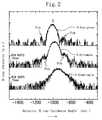
- Figure 1(a)illustrates respective thermal budgets of Si/Si 0.8 Ge 0.2 superlattice samples including or not including C based on the results of an X-ray diffraction (XRD) analysis.
- Figure 1(b)explains peaks resulting from basic diffraction and satellite peaks as represented by the XRD spectra.
- the XRD spectrum of an Si/Si 0.8 Ge 0.2 superlattice sample that was epitaxially grown and then subjected to neither ion implantation nor annealingis identified by SX as-grown.
- the XRD spectrum of an Si/Si 0.8 Ge 0.2 superlattice sample that was epitaxially grown, implanted with C ions and then subjected to rapid thermal annealing (RTA)is identified by SX C+impla.
- the XRD spectrum of an Si/Si 0.8 Ge 0.2 superlattice sample that was epitaxially grown and then just annealed, not implanted with C ionsis identified by SX non-impla.
- the axis of ordinatesrepresents the intensity of X-rays by the arbitrary unit, while the axis of abscissas represents the relative X-ray incidence angle by the second.
- ⁇satisfies higher-order conditions.
- FIG 4is a cross-sectional view illustrating the structure of a sample prepared for the XRD analysis.
- the sample used for the analysiswas a multilayer structure in which ten Si 0.8 Ge 0.2 layers containing Ge at 20% and ten Si layers were alternately stacked one upon the other on a silicon substrate by a UHV-CVD process. The thickness of each of these layers was 10 nm. That is to say, these layers correspond to 10 cycles.
- the 0 th -order peaksrepresents beams that have been reflected from the atomic faces themselves, while the 1 st , 2 nd , 3 rd -order peaks and so on represent the diffraction phenomenon of beams that have been reflected from the superlattice.
- the crystallinity of a samplecan be evaluated based on the half widths of respective peaks and the frequency of appearance of higher-order peaks.
- Figure 2illustrates, on a larger scale, portions of the XRD spectra shown in Figure 1(a) around peaks (0) to analyze the shapes of the 0 th -order peaks in further detail.
- peak (0)in the XRD spectrum SX non-impla . of the non-C-ion-implanted but annealed sample, peak (0) has its shape rounded and it half width broadened as a result of annealing.
- small peaks Poa and Pob observed on right- and left-hand sides of peak (0) in the spectrum SX as-grownhave collapsed completely in the spectrum SX non-impla .
- Figure 3illustrates concentrations of Ge in the respective superlattice samples to examine the stability of crystals that have been subjected to the RTA.
- the concentration profile of Ge in the epitaxially grown but non-implanted or annealed sampleis identified by the curve D as-grown .
- the concentration profile of Ge in the sample that was epitaxially grown, implanted with C ions and then subjected to RTA at 1000°C for 15 secondsis identified by the curve D C+impla .
- the concentration profile of Ge in the sample that was epitaxially grown and then subjected to RTA at 1000°C for 15 seconds without being implanted with C ionsis identified by the curve D non-impla .
- the Ge concentrationis very high in the Si 0.8 Ge 0.2 layer and low in the Si layer during the epitaxy.
- the concentration profile D non-impla .becomes gentler. That is to say, it can be seen that a great number of Ge atoms have moved into the Si layers.
- the concentration profile D C+impla . of the C-ion-implanted sampleis less gentle than the curve D non-impla . even after annealing has been carried out. This result shows that a smaller number of Ge atoms have moved into the Si layers.
- the Ge concentration profiles shown in Figure 3are gentler than the actual ones because there is a limit of measurement precision for every sample.
- the thickness of the Si 0.8 Ge 0.2 layerwas found increased by about 1.7 nm upward and downward. This increase was estimated based on a model where Ge atoms were supposed to be distributed over a region with a predetermined width around the interface. That is to say, as for the prior art semiconductor device including the Si/SiGe heterojunction, the results obtained were as if the width of the SiGe layer had apparently expanded due to the structural disorder of the Si/SiGe interface.
- Figures 5(a) and 5(b)illustrate how the interfacial structure changes through annealing for a sample not implanted with C ions and a sample implanted with C ions, respectively.
- Figure 5(a)if the sample is not implanted with C ions, then it is expected that a large number of Ge atoms would move, diffuse and segregate around the Si/SiO 2 interface located above as a result of annealing.
- the composition thereofgreatly changes locally around the interface and the Ge atoms and Si atoms (not shown) do not form crystal lattice but are arranged non-regularly in a disordered state.
- the C ion implantationsuppresses the movement and diffusion of Ge atoms.
- the movement and diffusion of Ge atomscan be suppressed and the interface can be kept definite and planar even if a device including the Si/SiGe heterojunction is annealed to activate the dopant.
- the number of Ge atoms segregated at the Si/SiO 2 interfacecan also be minimized.
- a semiconductor device including the Si/SiGe heterojunctioncan be fabricated by performing a smaller number of process steps with the gate electrode self-aligned with the source/drain regions.
- the movement and diffusion of Ge atoms in the SiGe layercan be suppressed even after the C atoms have moved into the Si layer.
- the structural disorder of the Si/SiGe interface due to the movement and diffusion of Ge atomsis suppressible if the C atoms have been introduced in advance into at least the Si layer.
- Figure 6(a)is a cross-sectional view illustrating a structure of an HMOS transistor according to a first embodiment of the present invention.
- Figure 6(b)is a cross-sectional view illustrating a structure of a region R10a shown in Figure 6(a) .
- the SiO 2 /Si interface and Si/Si 1-y Ge y interfacesare identified by the reference numerals 135 and 136 , respectively.
- the thickness of the i-Si 1-y Ge y layer 119is set equal to or less than the critical thickness thereof.
- the layers 118 and 119are in an equilibrium state with their crystallinity maintained and the mobility of carriers (holes) has been changed due to a compressive strain applied.
- the interfaceshould be kept definite and planar.
- the lower Si cap layer 118 containing Cis provided over the i-Si 1-y Ge y layer 119 .
- the concentration of C to be dopedshould not be high enough to adversely affect the characteristics of the transistor or the band structure thereof, e.g., about 1% or less.
- the interfacecan always be kept definite and planar throughout the process steps of stacking the respective layers and the annealing process to activate the dopant.
- the holescan be confined in a heterobarrier by utilizing the offset at the valence band.
- the Si/Si 1-y Ge y heterojunction deviceis applicable as a heterojunction PMOSFET.
- a negative voltageis applied to the gate electrode 116 , the polarity of the regions surrounding the Si/Si 1-y Ge y interface 136 is inverted, thus forming a p-channel, where positive carriers (holes) are confined, in the Si 1-y Ge y layer 119 .
- those carriersmove at a high velocity from the source 153 toward the drain region 154 .
- the Si/Si 1-y Ge y interface 136is planar, the p-channel is formed along the planar Si/Si 1-y Ge y interface 136 , and therefore, the carriers can move at an even higher velocity.
- the i-Si cap layer 142 not containing Cis formed on the lower i-Si cap layer 118 containing C.
- a gate oxide filmis formed by getting the i-Si cap layer 142 eroded with oxygen (i.e., by an oxidation process).
- the i-Si 1-y Ge y layer 119is epitaxially grown on the Si substrate 101 .
- the lower Si cap layer 118 containing C and i-Si cap layer 142 not containing Care stacked in this order on the i-Si 1-y Ge y layer 119 .
- Cmay be introduced into the lower Si cap layer 118 by ion implantation, CVD, UHV-CVD or MBE. If the ion implantation method is adopted, the C ion implantation may be performed in the middle of the process step shown in Figure 7(b) , i.e., after the lower Si cap layer 118 has been formed and before the i-Si cap layer 142 is formed.
- the i-Si cap layer 142is oxidized, thereby forming the SiO 2 film 117 to be the gate oxide film.
- the oxidationmay be stopped at about 750°C just before the Si/SiO 2 interface 135 reaches the lower Si cap layer 118 containing C while taking the diffusion rate of C and oxidation rate of Si into account.
- a p + -type polysilicon filmis deposited and then patterned, thereby forming the gate electrode 116 .
- carrier dopant ionse.g., boron fluoride (BF 2 + ) ions in this embodiment
- the source/drain regions 153 , 154are defined to be self-aligned with the gate electrode 116 (see Figure 6(a) ).
- a metal filmis deposited over the substrate and then patterned, thereby forming the source/drain contacts 151 , 152 .
- the movement and diffusion of Ge atoms around the Si/Si 1-y Ge y interface 136is suppressible thanks to the Ge atom movement inhibiting function of C.
- the interfacecan be kept definite and planar and various adverse effects, such as decline in reliability resulting from the segregation of Ge atoms around the SiO 2 film 117 during the formation of the gate oxide film, can be eliminated.
- Cmay be introduced into the lower Si cap layer 118 by ion implantation with low implant energy, CVD using methyl silane (SiH 3 CH 3 ), UHV-CVD or MBE.
- CVDmethyl silane
- UHV-CVDmethyl silane
- MBEmethyl silane
- Ccan be introduced into only the lower Si cap layer 118 . It should be noted, however, that C may be introduced into the i-Si 1-y Ge y layer 119 even if the CVD, UHV-CVD or MBE process is adopted.
- the dose of C to be introduced into the lower Si cap layer 118may be large to suppress the movement and diffusion of Ge atoms. Actually, though, it is known that once the concentration of C exceeds 1%, the crystal structures of Si and SiGe layers are adversely affected. Thus, to make the semiconductor device with the Si/SiGe heterojunction operate normally, the concentration of C is preferably 1% or less.
- Figure 8is a cross-sectional view illustrating part of a semiconductor device according to a second embodiment of the present invention.
- Figure 8illustrates a vertical cross section of a region R20b including gate electrode, gate insulating film and channel shown in Figure 9(b) , which is a multilayer structure applicable to both PMOS and NMOS transistor according to the second prior art example shown in Figure 14(a) .
- a valence bandcorresponding to a negative gate bias voltage applied.
- a conduction bandcorresponding to a positive gate bias voltage applied.
- Si 1-x Ge x buffer layer 123 , i-Si 1-x Ge x spacer layer 121 , ⁇ -doped layer 122 , i-Si layer 120 containing C, i-Si 1-y Ge y layer 119 (where 0 ⁇ y ⁇ 1, e.g., y0.2), lower Si cap layer 118 containing C, i-Si cap layer 142 , SiO 2 layer 117 functioning as a gate insulating film and polysilicon gate electrode 116 are stacked in this order.
- SiO 2 /Si interface and first, second and third interfacesare identified by the reference numerals 135 , 137 , 138 and 139 , respectively.
- Ge, C and dopant atomsare identified by the reference numerals 106 , 107 and 143 , respectively.
- an HCMOS deviceis made up of n- and p-channel MOS transistors each including the Si 1-y Ge y layer 119 as in the second prior art example. Also, according to this embodiment, superior conductivity is attainable compared to a homojunction transistor formed on an Si substrate. In addition, since the n- and p-channel MOS transistors are formed using a common multilayer structure, the fabrication process thereof is simplified.
- the ⁇ -doped layer 122 for supplying carriers to the n-channelis defined within the i-Si 1-x Ge x spacer layer 121 .
- the SiO 2 layer 117 as the gate oxide film and the gate electrode 116are formed in this order via the i-Si cap layer 142 interposed therebetween.
- a valence bandappearing when a negative gate bias voltage is applied to the multi-layered transistor shown in the center of Figure 8 to make the transistor operate as PMOSFET.
- a conduction bandappearing when a positive gate bias voltage is applied to the multilayered transistor to make the transistor operate as NMOSFET. That is to say, one of the transistors can be operated as PMOSFET and the other as NMOSFET by using the same multilayer structure.
- holesare confined in the p-channel by utilizing the offset at the valence band in the first interface 137 between the i-Si 1-y Ge y layer 119 and the i-Si cap layer 118 . And a negative gate bias voltage is applied to the gate electrode 116 , thereby making the holes move.
- the magnitude of the strainis adjusted by changing the Ge mole fraction in the i-Si 1-y Ge y layer 119 , then the band offset at the first interface 137 is controllable.
- Figure 9(a) and 9(b)are cross-sectional views illustrating part of a semiconductor device fabrication process according to the second embodiment.
- the same process steps as those of the second prior art examplemay be performed to form a portion under the channel.
- the ⁇ -doped layer 122is formed in the i-Si 1-x Ge x spacer layer 121 by locally introducing dopant ions into the layer 121 during the epitaxial growth thereof.
- Cmay be introduced into the i-Si layer 120 and lower Si layer 118 by ion implantation, CVD, UHV-CVD or MBE.
- Cmay be implanted into the i-Si layer 120 with low implant energy applied just after the i-Si layer 120 has been formed.
- Cmay be implanted after the i-Si 1-y Ge y layer 119 and the lower Si cap layer 118 have been formed on the i-Si layer 120 such that C is contained in all of the i-Si layer 120 , i-Si 1-y Ge y layer 119 and lower Si cap layer 118 .
- the implantation processmay be performed just once. If the CVD process is adopted, then a gas containing methyl silane (SiH 3 CH 3 ) may be used.
- the i-Si cap layer 142is oxidized, thereby forming the SiO 2 film 117 to be the gate oxide film.
- the oxidationmay be stopped at about 750°C just before the Si/SiO 2 interface 135 reaches the lower Si cap layer 118 containing C while taking the diffusion rate of C and oxidation rate of Si into account.
- a p + -type polysilicon filmis deposited and then patterned, thereby forming the gate electrode 116 .
- carrier dopant ionse.g., boron fluoride (BF 2 + ) ions in this embodiment
- the source/drain regions 153 , 154are defined to be self-aligned with the gate electrode 116 (see Figure 6(a) ).
- a metal filmis deposited over the substrate and then patterned, thereby forming the source/drain contacts 151 , 152 .
- the i-Si layer 120 and the lower Si cap layer 118are doped with C unlike the second prior art example.
- neither structural disorder nor lattice defectsare brought about in the interfaces 137 , 138 and 139 because the movement and diffusion of Ge atoms are suppressed.
- the reliability of the gate insulating filmis not risked by the segregation of the Ge atoms 106 to the Si/SiO 2 interface 135 .
- the same multilayer structurecan be selectively used as NMOSFET or PMOSFET by changing the direction of the gate bias voltage. Accordingly, an HCMOS device with excellent conductivity can be obtained through relatively simple process steps if a single multilayer structure is separated and isolated via the STI to define separate source/drain regions and gate electrode.
- the preferable range of the C concentrationis as described in the first embodiment.
- Figure 10is a cross-sectional view illustrating part of a semiconductor device (or HMOS transistor) according to a third embodiment of the present invention, in which C contained in the Si layer above the Si/SiGe interface has a concentration gradient.
- the cross section illustrated in Figure 10corresponds to the region R10a shown in Figure 6(a) .
- the SiO 2 /Si interface and Si/Si 1-y Ge y interfacesare identified by the reference numerals 135 and 136 , respectively.
- the HMOS transistor according to the third embodimenthas substantially the same structure as that of the HMOS transistor shown in Figures 6(a) and 6(b) .
- C contained in the lower Si cap layer 118has a concentration gradient as shown on the right-hand side of Figure 10 .
- the C concentration in the lower Si cap layer 118is maximum around the Si/SiGe interface 136 , decreases monotonically from the interface 136 toward the i-Si cap layer 142 and finally reaches substantially zero at the interface between the lower Si cap layer 118 and i-Si cap layer 142 .
- Such a concentration profile of Ccan be obtained by gradually decreasing the content of carbon-forming gas in the source gases when the lower Si cap layer 118 is formed by CVD, UHV-CVD or MBE process.
- the same effects as those of the first embodimentare also attainable.
- the C concentrationis almost zero at the interface between the lower Si cap layer 118 and the i-Si cap layer 142 , it is possible to prevent the C atoms from reaching the SiO 2 layer 117 . Accordingly, decline in reliability of the SiO 2 layer 117 and decrease in carrier mobility, which results from the formation of interface levels, can be both prevented.
- Figure 11is a cross-sectional view illustrating part of a semiconductor device (i.e., HCMOS device) according to a fourth embodiment of the present invention.
- a semiconductor devicei.e., HCMOS device
- both the Si layers 118 and 120 above the two Si/SiGe interfaces 137 and 139have graded C concentration profiles.
- Figure 11corresponds to the region R20b according to the second embodiment shown in Figure 8 but illustrates a larger region covering the gate electrode and buffer layer.
- the Si 1-x Ge x (where x0.3) buffer layer 123 of which the strain has been relaxed, i-Si 1-x Ge x spacer layer 121 , ⁇ -doped layer 122 , i-Si layer 120 containing C with a graded concentration profile, i-Si 1-y Ge y layer 119 (where 0 ⁇ y ⁇ 1) containing Ge with a graded concentration profile, lower Si cap layer 118 containing C with a graded concentration profile, i-Si cap layer 142 , SiO 2 layer 117 functioning as a gate insulating film and polysilicon gate electrode 116 are stacked in this order.
- SiO 2 /Si interface and first, second and third interfacesare identified by the reference numerals 135 , 137 , 138 and 139 , respectively.
- Ge, C and dopant atomsare identified by the reference numerals 106 , 107 and 143 , respectively.
- an HCMOS deviceis made up of n- and p-channel MOS transistors each including the Si 1-y Ge y layer 119 as in the second prior art example. Also, according to this embodiment, superior conductivity is attainable compared to a homojunction transistor formed on an Si substrate. In addition, since the n- and p-channel MOS transistors are formed using a common multilayer structure, the fabrication process thereof is simplified.
- the HCMOS device according to the fourth embodimenthas substantially the same structure as, but different in some respect from, the HCMOS device according to the second embodiment shown in Figure 8 .
- these respectswill be described with reference to Figures 12(a) and 12(b) .
- the C concentration in the lower Si cap layer 118is maximum around the Si/SiGe interface 137 , decreases monotonically from the Si/SiGe interface 137 toward the i-Si cap layer 142 and finally reaches substantially zero at the interface between the lower Si cap layer 118 and i-Si cap layer 142 .
- the concentration of Chas such a profile, then adverse effects of C on the SiO 2 layer 117 can be avoided substantially.
- the Ge content in the i-Si 1-y Ge y layer 119increases from the second to first interface 138 to 137 .
- the energy level Ev at the edge of the valence bandcan be modified and the depth of the p-channel formed in the first interface 137 for confining holes therein can be adjusted, thus making the threshold voltage of the PMOSFET freely controllable.
- the characteristic value of the PMOSFETcan be optimized because the characteristics of the NMOSFET are not affected at all.
- the number of carriers flowing into a parasitic channel formed around the Si/SiO 2 interface 135can be reduced and the mobility thereof can be increased.
- the concentration of C in the i-Si layer 120has such a profile as gradually decreasing from the third toward the second interface 139 to 138 .
- a positive voltageis applied to the gate electrode 116 , an n-channel is formed in the i-Si layer 120 at a location closer to the SiGe spacer layer 121 that has been delta-doped with the dopant atoms 143 .
- carrierscan be created more efficiently, the driving power of the NMOSFET can be increased and the threshold voltage of the NMOSFET can be regulated.
- the strainhas a magnitude of 0.35t.
- the energy level Ec at the edge of the conduction band of Si containing Cshifts from that of Si not containing C toward the valence band by -4.9t (eV).
- the energy level Ev at the edge of the valence bandshifts toward the conduction band by -1.5t (eV).
- the concentration tis changed from 0.03% to 0%, for example, then the energy level Ev at the edge of the valence band shifts toward the conduction band by about 45 meV.
- the i-Si layer 120 containing Cis formed on the Si 1-x Ge x layer with a relaxed strain and a tensile strain is applied to the i-Si layer 120 . Accordingly, the band structure of the i-Si layer 120 receiving the tensile strain also changes similarly, although the change of band structure depends on the Ge content in the underlying Si 1-x Ge x layer (i.e., the i-Si 1-x Ge x spacer layer 121 in this case).
- the energy level Ec at the edge of the conduction band around the n-channelis controllable.
- the threshold voltage of the NMOSFETcan be controlled more freely without affecting the characteristics of the PMOSFET at all.
- Such a concentration profile of Ccan be obtained by gradually decreasing the content of carbon-forming gas in the source gases when the lower Si cap layer 118 and i-Si layer 120 are formed by CVD, UHV-CVD or MBE process.
- both of the C concentration profiles in the lower Si cap layer 118 and the i-Si layer 120are graded.
- only one of these C concentration profilesmay be graded, while the other may be substantially uniform.
Landscapes
- Physics & Mathematics (AREA)
- Engineering & Computer Science (AREA)
- High Energy & Nuclear Physics (AREA)
- General Physics & Mathematics (AREA)
- Toxicology (AREA)
- Condensed Matter Physics & Semiconductors (AREA)
- Health & Medical Sciences (AREA)
- Manufacturing & Machinery (AREA)
- Computer Hardware Design (AREA)
- Microelectronics & Electronic Packaging (AREA)
- Power Engineering (AREA)
- Spectroscopy & Molecular Physics (AREA)
- Insulated Gate Type Field-Effect Transistor (AREA)
- Metal-Oxide And Bipolar Metal-Oxide Semiconductor Integrated Circuits (AREA)
- Thin Film Transistor (AREA)
Abstract
Description
Claims (23)
- A semiconductor device comprising:a semiconductor substrate;a first semiconductor layer, which is formed within thesemiconductor substrate and is made of mixed crystals of multipleelements; anda second semiconductor layer, which is formed within thesemiconductor substrate to be in contact with the first semiconductorlayer and contains an inhibitor for suppressingmovement of at least one of the constituent elements of thefirst semiconductor layer,
wherein the semiconductor device functions as a deviceusing a heterojunction formed between the first and secondsemiconductor layers. - The device of Claim 1, wherein the first semiconductorlayer is made of Si1-yGey, where 0<y<1, the second semiconductorlayer is made of Si, and the inhibitor is C.
- The device of Claim 2, wherein the concentration of Cis 1% or less.
- The device of Claim 2, wherein the Si layer is locatedcloser to the surface of the semiconductor substrate thanthe Si1-yGey layer is, and
wherein a concentration of C in the Si layer has such aprofile as decreasing from the Si1-yGey layer toward the surfaceof the semiconductor substrate. - The device of Claim 2, wherein the Si1-yGey layer has athickness equal to or smaller than its critical thickness, andreceives a compressive strain.
- The device of Claim 2, which is a field effect transistorfurther comprising:a gate electrode formed on the semiconductor substrate;anda channel formed in the Si layer under the gate electrode.
- The device of Claim 6, further comprising a gate insulatingfilm interposed between the gate electrode and theSi layer.
- The device of Claim 7, further comprising an intrinsicSi layer interposed between the Si layer and the gate insulatingfilm.
- The device of Claim 6, wherein the Si layer is locatedcloser to the surface of the semiconductor substrate than the Si1-yGey layer is, and
wherein a concentration of C in the Si layer has such aprofile as decreasing from the Si1-yGey layer toward the surfaceof the semiconductor substrate. - The device of Claim 2, wherein the Si layer is locatedcloser to the surface of the semiconductor substratethan the Si1-yGey layer is, and
wherein the device further comprises:a second Si layer, which is formed under the Si1-yGeylayer and contains C;an Si1-xGex layer formed under the second Si layer, where0<x<1; anda δ-doped layer, which is formed within the Si1-xGexlayer in a region thereof closer to the second Si layer andcontains a high-concentration carrier dopant, and
wherein the semiconductor device is a CMOS device including:a p-channel field effect transistor, which includes agate electrode and a p-channel, the gate electrode beingformed on the semiconductor substrate, the p-channel beingdefined in the Si1-xGex layer under the gate electrode; andan n-channel field effect transistor, which includes agate electrode and an n-channel, the gate electrode beingformed on the semiconductor substrate, the n-channel being defined in the Si layer under the gate electrode. - The device of Claim 10, wherein the Si and second Silayers receive a tensile strain, and
wherein a strain applied to the Si1-xGex layer has beenrelaxed. - The device of Claim 10, further comprising gate insulatingfilms formed between the gate electrodes of the p- andn-channel field effect transistors and the Si layer, respectively.
- The device of Claim 12, further comprising intrinsicSi layers formed between the gate insulating films of the p- andn-channel field effect transistors and the Si layer, respectively.
- The device of Claim 12, wherein a concentration of Cin the Si layer has such a profile as decreasing from theSi1-yGey layer toward the surface of the semiconductor substrate.
- The device of Claim 10, wherein a concentration of Cin the second Si layer has such a profile as decreasing fromthe Si1-xGex layer toward the Si1-yGey layer.
- The device of Claim 10, wherein a content of Ge inthe Si1-yGey layer increases from the second Si layer toward theSi layer.
- A method for fabricating a semiconductor device,comprising the steps of:a) forming a first semiconductor layer, which is made ofmixed crystals of multiple elements, on a substrate;b) forming a second semiconductor layer on the firstsemiconductor layer; andc) doping the first and second semiconductor layers withan inhibitor by implanting ions of the inhibitor thereto, theinhibitor suppressing movement of at least one of the constituentelements of the first semiconductor layer,
wherein the step c) is performed after the step b) hasbeen performed, and
wherein the semiconductor device functions as a deviceusing a heterojunction formed between the first and secondsemiconductor layers. - The method of Claim 17, wherein the first semiconductorlayer is made of Si1-yGey, where 0<y<1, the secondsemiconductor layer is made of Si, and the inhibitor is C.
- The method of Claim 18, further comprising the steps of:forming an intrinsic Si layer on the Si layer after thestep b) has been performed and before the step c) is performed;andforming an oxide film substantially reaching the Silayer by oxidizing the intrinsic Si layer after the step c)has been performed.
- A method for fabricating a semiconductor device,comprising the steps of:a) forming a first semiconductor layer, which is made ofmixed crystals of multiple elements, on a substrate; andb) forming a second semiconductor layer, which containsan inhibitor, on the first semiconductor layer such that theconcentration of the inhibitor in the second semiconductorlayer decreases upward, the inhibitor suppressing movement ofat least one of the constituent elements of the first semiconductorlayer,
wherein the semiconductor device functions as a deviceusing a heterojunction formed between the first and secondsemiconductor layers. - The method of Claim 20, wherein in the step b), CVD,UHV-CVD or MBE process is performed.
- The method of Claim 20 or 21, wherein the firstsemiconductor layer is made of Si1-yGey, where 0<y<1, the secondsemiconductor layer is made of Si, and the inhibitor isC.
- The method of Claim 22, further comprising the stepsof:forming an intrinsic Si layer on the Si layer after thestep b) has been performed; andforming an oxide film substantially reaching the Silayer by oxidizing the intrinsic Si layer.
Applications Claiming Priority (2)
| Application Number | Priority Date | Filing Date | Title |
|---|---|---|---|
| JP764199 | 1999-01-14 | ||
| JP764199 | 1999-01-14 |
Publications (3)
| Publication Number | Publication Date |
|---|---|
| EP1020900A2true EP1020900A2 (en) | 2000-07-19 |
| EP1020900A3 EP1020900A3 (en) | 2000-09-20 |
| EP1020900B1 EP1020900B1 (en) | 2009-08-05 |
Family
ID=11671466
Family Applications (1)
| Application Number | Title | Priority Date | Filing Date |
|---|---|---|---|
| EP00100592AExpired - LifetimeEP1020900B1 (en) | 1999-01-14 | 2000-01-12 | Semiconductor device and method for fabricating the same |
Country Status (7)
| Country | Link |
|---|---|
| US (2) | US6597016B1 (en) |
| EP (1) | EP1020900B1 (en) |
| JP (1) | JP3592981B2 (en) |
| KR (1) | KR100648769B1 (en) |
| CN (1) | CN1184694C (en) |
| DE (1) | DE60042666D1 (en) |
| TW (1) | TW439300B (en) |
Cited By (32)
| Publication number | Priority date | Publication date | Assignee | Title |
|---|---|---|---|---|
| WO2002071488A1 (en)* | 2001-03-02 | 2002-09-12 | Amberwave Systems Corporation | Relaxed silicon germanium platform for high speed cmos electronics and high speed analog circuits |
| US6555839B2 (en) | 2000-05-26 | 2003-04-29 | Amberwave Systems Corporation | Buried channel strained silicon FET using a supply layer created through ion implantation |
| US6593641B1 (en) | 2001-03-02 | 2003-07-15 | Amberwave Systems Corporation | Relaxed silicon germanium platform for high speed CMOS electronics and high speed analog circuits |
| WO2003015138A3 (en)* | 2001-08-09 | 2003-11-06 | Amberwave Systems Corp | Optimized buried-channel fets based on sige heterostructures |
| US6646322B2 (en) | 2001-03-02 | 2003-11-11 | Amberwave Systems Corporation | Relaxed silicon germanium platform for high speed CMOS electronics and high speed analog circuits |
| WO2003028106A3 (en)* | 2001-09-24 | 2003-11-13 | Amberwave Systems Corp | Rf circuits including transistors having strained material layers |
| US6724008B2 (en) | 2001-03-02 | 2004-04-20 | Amberwave Systems Corporation | Relaxed silicon germanium platform for high speed CMOS electronics and high speed analog circuits |
| US6730551B2 (en) | 2001-08-06 | 2004-05-04 | Massachusetts Institute Of Technology | Formation of planar strained layers |
| EP1381088A4 (en)* | 2001-04-18 | 2004-07-07 | Matsushita Electric Industrial Co Ltd | SEMICONDUCTOR DEVICE |
| US6830976B2 (en) | 2001-03-02 | 2004-12-14 | Amberwave Systems Corproation | Relaxed silicon germanium platform for high speed CMOS electronics and high speed analog circuits |
| US6876010B1 (en) | 1997-06-24 | 2005-04-05 | Massachusetts Institute Of Technology | Controlling threading dislocation densities in Ge on Si using graded GeSi layers and planarization |
| US6900094B2 (en) | 2001-06-14 | 2005-05-31 | Amberwave Systems Corporation | Method of selective removal of SiGe alloys |
| US6900103B2 (en) | 2001-03-02 | 2005-05-31 | Amberwave Systems Corporation | Relaxed silicon germanium platform for high speed CMOS electronics and high speed analog circuits |
| US6916727B2 (en) | 2001-06-21 | 2005-07-12 | Massachusetts Institute Of Technology | Enhancement of P-type metal-oxide-semiconductor field effect transistors |
| US6974735B2 (en) | 2001-08-09 | 2005-12-13 | Amberwave Systems Corporation | Dual layer Semiconductor Devices |
| WO2005124837A1 (en)* | 2004-06-16 | 2005-12-29 | Koninklijke Philips Electronics N.V. | Method of manufacturing a strained semiconductor layer, method of manufacturing a semiconductor device and semiconductor substrate suitable for use in such a method |
| US7074623B2 (en) | 2002-06-07 | 2006-07-11 | Amberwave Systems Corporation | Methods of forming strained-semiconductor-on-insulator finFET device structures |
| US7122449B2 (en) | 2002-06-10 | 2006-10-17 | Amberwave Systems Corporation | Methods of fabricating semiconductor structures having epitaxially grown source and drain elements |
| US7138310B2 (en) | 2002-06-07 | 2006-11-21 | Amberwave Systems Corporation | Semiconductor devices having strained dual channel layers |
| US7138649B2 (en) | 2001-08-09 | 2006-11-21 | Amberwave Systems Corporation | Dual-channel CMOS transistors with differentially strained channels |
| US7217603B2 (en) | 2002-06-25 | 2007-05-15 | Amberwave Systems Corporation | Methods of forming reacted conductive gate electrodes |
| US7256142B2 (en) | 2001-03-02 | 2007-08-14 | Amberwave Systems Corporation | Relaxed SiGe platform for high speed CMOS electronics and high speed analog circuits |
| US7259388B2 (en) | 2002-06-07 | 2007-08-21 | Amberwave Systems Corporation | Strained-semiconductor-on-insulator device structures |
| US7259108B2 (en) | 2002-03-14 | 2007-08-21 | Amberwave Systems Corporation | Methods for fabricating strained layers on semiconductor substrates |
| US7301180B2 (en) | 2001-06-18 | 2007-11-27 | Massachusetts Institute Of Technology | Structure and method for a high-speed semiconductor device having a Ge channel layer |
| US7307273B2 (en) | 2002-06-07 | 2007-12-11 | Amberwave Systems Corporation | Control of strain in device layers by selective relaxation |
| US7332417B2 (en) | 2003-01-27 | 2008-02-19 | Amberwave Systems Corporation | Semiconductor structures with structural homogeneity |
| US7335545B2 (en) | 2002-06-07 | 2008-02-26 | Amberwave Systems Corporation | Control of strain in device layers by prevention of relaxation |
| US7393733B2 (en) | 2004-12-01 | 2008-07-01 | Amberwave Systems Corporation | Methods of forming hybrid fin field-effect transistor structures |
| US7504704B2 (en) | 2003-03-07 | 2009-03-17 | Amberwave Systems Corporation | Shallow trench isolation process |
| US7615829B2 (en) | 2002-06-07 | 2009-11-10 | Amberwave Systems Corporation | Elevated source and drain elements for strained-channel heterojuntion field-effect transistors |
| US7776697B2 (en) | 2001-09-21 | 2010-08-17 | Taiwan Semiconductor Manufacturing Company, Ltd. | Semiconductor structures employing strained material layers with defined impurity gradients and methods for fabricating same |
Families Citing this family (89)
| Publication number | Priority date | Publication date | Assignee | Title |
|---|---|---|---|---|
| US7227176B2 (en) | 1998-04-10 | 2007-06-05 | Massachusetts Institute Of Technology | Etch stop layer system |
| DE60042666D1 (en)* | 1999-01-14 | 2009-09-17 | Panasonic Corp | Semiconductor component and method for its production |
| US6993222B2 (en) | 1999-03-03 | 2006-01-31 | Rj Mears, Llc | Optical filter device with aperiodically arranged grating elements |
| GB2385981B (en) | 1999-03-05 | 2003-11-05 | Nanovis Llc | Laser with aperiodic grating |
| US6602613B1 (en) | 2000-01-20 | 2003-08-05 | Amberwave Systems Corporation | Heterointegration of materials using deposition and bonding |
| JP2003520444A (en) | 2000-01-20 | 2003-07-02 | アンバーウェーブ システムズ コーポレイション | Low threading dislocation density lattice-mismatched epilayer that does not require high-temperature growth |
| US6573126B2 (en) | 2000-08-16 | 2003-06-03 | Massachusetts Institute Of Technology | Process for producing semiconductor article using graded epitaxial growth |
| US6649480B2 (en) | 2000-12-04 | 2003-11-18 | Amberwave Systems Corporation | Method of fabricating CMOS inverter and integrated circuits utilizing strained silicon surface channel MOSFETs |
| US6426265B1 (en)* | 2001-01-30 | 2002-07-30 | International Business Machines Corporation | Incorporation of carbon in silicon/silicon germanium epitaxial layer to enhance yield for Si-Ge bipolar technology |
| US6723661B2 (en) | 2001-03-02 | 2004-04-20 | Amberwave Systems Corporation | Relaxed silicon germanium platform for high speed CMOS electronics and high speed analog circuits |
| WO2002082514A1 (en) | 2001-04-04 | 2002-10-17 | Massachusetts Institute Of Technology | A method for semiconductor device fabrication |
| KR100426956B1 (en)* | 2001-07-23 | 2004-04-17 | 한국과학기술원 | Formation method for oxidation film of SiGe epitaxial layer |
| KR100409435B1 (en)* | 2002-05-07 | 2003-12-18 | 한국전자통신연구원 | Method of manufacturing an active layer and a method for manufacturing a MOS transistor using the same |
| US20030227057A1 (en) | 2002-06-07 | 2003-12-11 | Lochtefeld Anthony J. | Strained-semiconductor-on-insulator device structures |
| AU2003274922A1 (en) | 2002-08-23 | 2004-03-11 | Amberwave Systems Corporation | Semiconductor heterostructures having reduced dislocation pile-ups and related methods |
| US7594967B2 (en) | 2002-08-30 | 2009-09-29 | Amberwave Systems Corporation | Reduction of dislocation pile-up formation during relaxed lattice-mismatched epitaxy |
| US7098095B1 (en) | 2002-12-10 | 2006-08-29 | National Semiconductor Corporation | Method of forming a MOS transistor with a layer of silicon germanium carbon |
| US6818938B1 (en)* | 2002-12-10 | 2004-11-16 | National Semiconductor Corporation | MOS transistor and method of forming the transistor with a channel region in a layer of composite material |
| FR2853452B1 (en)* | 2003-04-01 | 2005-08-19 | St Microelectronics Sa | METHOD FOR MANUFACTURING A SEMICONDUCTOR DEVICE COMPRISING A GRID DIELECTRIC IN MATERIAL WITH HIGH DIELECTRIC PERMITTIVITY |
| JP4445213B2 (en) | 2003-05-12 | 2010-04-07 | 株式会社日立製作所 | Semiconductor device |
| US20050282330A1 (en)* | 2003-06-26 | 2005-12-22 | Rj Mears, Llc | Method for making a semiconductor device including a superlattice having at least one group of substantially undoped layers |
| US20060267130A1 (en)* | 2003-06-26 | 2006-11-30 | Rj Mears, Llc | Semiconductor Device Including Shallow Trench Isolation (STI) Regions with a Superlattice Therebetween |
| US20070063185A1 (en)* | 2003-06-26 | 2007-03-22 | Rj Mears, Llc | Semiconductor device including a front side strained superlattice layer and a back side stress layer |
| US20060289049A1 (en)* | 2003-06-26 | 2006-12-28 | Rj Mears, Llc | Semiconductor Device Having a Semiconductor-on-Insulator (SOI) Configuration and Including a Superlattice on a Thin Semiconductor Layer |
| US20060231857A1 (en)* | 2003-06-26 | 2006-10-19 | Rj Mears, Llc | Method for making a semiconductor device including a memory cell with a negative differential resistance (ndr) device |
| US7229902B2 (en)* | 2003-06-26 | 2007-06-12 | Rj Mears, Llc | Method for making a semiconductor device including a superlattice with regions defining a semiconductor junction |
| US7531828B2 (en)* | 2003-06-26 | 2009-05-12 | Mears Technologies, Inc. | Semiconductor device including a strained superlattice between at least one pair of spaced apart stress regions |
| US20060243964A1 (en)* | 2003-06-26 | 2006-11-02 | Rj Mears, Llc | Method for making a semiconductor device having a semiconductor-on-insulator configuration and a superlattice |
| US20070063186A1 (en)* | 2003-06-26 | 2007-03-22 | Rj Mears, Llc | Method for making a semiconductor device including a front side strained superlattice layer and a back side stress layer |
| US7598515B2 (en)* | 2003-06-26 | 2009-10-06 | Mears Technologies, Inc. | Semiconductor device including a strained superlattice and overlying stress layer and related methods |
| US20060273299A1 (en)* | 2003-06-26 | 2006-12-07 | Rj Mears, Llc | Method for making a semiconductor device including a dopant blocking superlattice |
| US7227174B2 (en)* | 2003-06-26 | 2007-06-05 | Rj Mears, Llc | Semiconductor device including a superlattice and adjacent semiconductor layer with doped regions defining a semiconductor junction |
| US6897472B2 (en)* | 2003-06-26 | 2005-05-24 | Rj Mears, Llc | Semiconductor device including MOSFET having band-engineered superlattice |
| US7586165B2 (en)* | 2003-06-26 | 2009-09-08 | Mears Technologies, Inc. | Microelectromechanical systems (MEMS) device including a superlattice |
| US20070015344A1 (en)* | 2003-06-26 | 2007-01-18 | Rj Mears, Llc | Method for Making a Semiconductor Device Including a Strained Superlattice Between at Least One Pair of Spaced Apart Stress Regions |
| US7531850B2 (en)* | 2003-06-26 | 2009-05-12 | Mears Technologies, Inc. | Semiconductor device including a memory cell with a negative differential resistance (NDR) device |
| US20040266116A1 (en)* | 2003-06-26 | 2004-12-30 | Rj Mears, Llc | Methods of fabricating semiconductor structures having improved conductivity effective mass |
| US6878576B1 (en) | 2003-06-26 | 2005-04-12 | Rj Mears, Llc | Method for making semiconductor device including band-engineered superlattice |
| US20050279991A1 (en)* | 2003-06-26 | 2005-12-22 | Rj Mears, Llc | Semiconductor device including a superlattice having at least one group of substantially undoped layers |
| US20070010040A1 (en)* | 2003-06-26 | 2007-01-11 | Rj Mears, Llc | Method for Making a Semiconductor Device Including a Strained Superlattice Layer Above a Stress Layer |
| US7491587B2 (en)* | 2003-06-26 | 2009-02-17 | Mears Technologies, Inc. | Method for making a semiconductor device having a semiconductor-on-insulator (SOI) configuration and including a superlattice on a thin semiconductor layer |
| US20060011905A1 (en)* | 2003-06-26 | 2006-01-19 | Rj Mears, Llc | Semiconductor device comprising a superlattice dielectric interface layer |
| US7586116B2 (en)* | 2003-06-26 | 2009-09-08 | Mears Technologies, Inc. | Semiconductor device having a semiconductor-on-insulator configuration and a superlattice |
| US7659539B2 (en) | 2003-06-26 | 2010-02-09 | Mears Technologies, Inc. | Semiconductor device including a floating gate memory cell with a superlattice channel |
| US7045377B2 (en)* | 2003-06-26 | 2006-05-16 | Rj Mears, Llc | Method for making a semiconductor device including a superlattice and adjacent semiconductor layer with doped regions defining a semiconductor junction |
| JP2007521648A (en)* | 2003-06-26 | 2007-08-02 | アール.ジェイ. メアーズ エルエルシー | Semiconductor device having MOSFET with band design superlattice |
| US20070020833A1 (en)* | 2003-06-26 | 2007-01-25 | Rj Mears, Llc | Method for Making a Semiconductor Device Including a Channel with a Non-Semiconductor Layer Monolayer |
| US7153763B2 (en) | 2003-06-26 | 2006-12-26 | Rj Mears, Llc | Method for making a semiconductor device including band-engineered superlattice using intermediate annealing |
| US7531829B2 (en)* | 2003-06-26 | 2009-05-12 | Mears Technologies, Inc. | Semiconductor device including regions of band-engineered semiconductor superlattice to reduce device-on resistance |
| US20060220118A1 (en)* | 2003-06-26 | 2006-10-05 | Rj Mears, Llc | Semiconductor device including a dopant blocking superlattice |
| US7535041B2 (en)* | 2003-06-26 | 2009-05-19 | Mears Technologies, Inc. | Method for making a semiconductor device including regions of band-engineered semiconductor superlattice to reduce device-on resistance |
| US7446002B2 (en)* | 2003-06-26 | 2008-11-04 | Mears Technologies, Inc. | Method for making a semiconductor device comprising a superlattice dielectric interface layer |
| US7045813B2 (en)* | 2003-06-26 | 2006-05-16 | Rj Mears, Llc | Semiconductor device including a superlattice with regions defining a semiconductor junction |
| US7202494B2 (en)* | 2003-06-26 | 2007-04-10 | Rj Mears, Llc | FINFET including a superlattice |
| US20060292765A1 (en)* | 2003-06-26 | 2006-12-28 | Rj Mears, Llc | Method for Making a FINFET Including a Superlattice |
| US7612366B2 (en)* | 2003-06-26 | 2009-11-03 | Mears Technologies, Inc. | Semiconductor device including a strained superlattice layer above a stress layer |
| US7514328B2 (en)* | 2003-06-26 | 2009-04-07 | Mears Technologies, Inc. | Method for making a semiconductor device including shallow trench isolation (STI) regions with a superlattice therebetween |
| US20070020860A1 (en)* | 2003-06-26 | 2007-01-25 | Rj Mears, Llc | Method for Making Semiconductor Device Including a Strained Superlattice and Overlying Stress Layer and Related Methods |
| DE10360874B4 (en)* | 2003-12-23 | 2009-06-04 | Infineon Technologies Ag | Field effect transistor with hetero-layer structure and associated production method |
| JP2005209980A (en)* | 2004-01-26 | 2005-08-04 | Sony Corp | Semiconductor device and method for manufacturing the same |
| US20050274988A1 (en)* | 2004-06-01 | 2005-12-15 | Hong Sungkwon C | Imager with reflector mirrors |
| US20060118892A1 (en)* | 2004-12-02 | 2006-06-08 | Taiwan Semiconductor Manufacturing Company, Ltd. | Methods and Structures to Produce a Strain-Inducing Layer in a Semiconductor Device |
| WO2006097977A1 (en)* | 2005-03-11 | 2006-09-21 | Fujitsu Limited | Semiconductor device and method for manufacturing same |
| WO2007076008A2 (en)* | 2005-12-22 | 2007-07-05 | Mears Technologies, Inc | Electronic device including a poled superlattice having a net electrical dipole moment and associated methods |
| US7517702B2 (en)* | 2005-12-22 | 2009-04-14 | Mears Technologies, Inc. | Method for making an electronic device including a poled superlattice having a net electrical dipole moment |
| WO2007098138A2 (en)* | 2006-02-21 | 2007-08-30 | Mears Technologies, Inc. | Semiconductor device comprising a lattice matching layer and associated methods |
| JP4182986B2 (en)* | 2006-04-19 | 2008-11-19 | トヨタ自動車株式会社 | Semiconductor device and manufacturing method thereof |
| DE602006013106D1 (en)* | 2006-06-13 | 2010-05-06 | Hitachi Ltd | Magnetoresistance device |
| US7772060B2 (en)* | 2006-06-21 | 2010-08-10 | Texas Instruments Deutschland Gmbh | Integrated SiGe NMOS and PMOS transistors |
| US7781827B2 (en) | 2007-01-24 | 2010-08-24 | Mears Technologies, Inc. | Semiconductor device with a vertical MOSFET including a superlattice and related methods |
| US7928425B2 (en)* | 2007-01-25 | 2011-04-19 | Mears Technologies, Inc. | Semiconductor device including a metal-to-semiconductor superlattice interface layer and related methods |
| US7880161B2 (en)* | 2007-02-16 | 2011-02-01 | Mears Technologies, Inc. | Multiple-wavelength opto-electronic device including a superlattice |
| US7863066B2 (en)* | 2007-02-16 | 2011-01-04 | Mears Technologies, Inc. | Method for making a multiple-wavelength opto-electronic device including a superlattice |
| US7812339B2 (en)* | 2007-04-23 | 2010-10-12 | Mears Technologies, Inc. | Method for making a semiconductor device including shallow trench isolation (STI) regions with maskless superlattice deposition following STI formation and related structures |
| US7879678B2 (en)* | 2008-02-28 | 2011-02-01 | Versatilis Llc | Methods of enhancing performance of field-effect transistors and field-effect transistors made thereby |
| DE102010046215B4 (en) | 2010-09-21 | 2019-01-03 | Infineon Technologies Austria Ag | Semiconductor body with strained region, electronic component and a method for producing the semiconductor body. |
| CN103579308B (en)* | 2012-07-27 | 2016-08-10 | 中芯国际集成电路制造(上海)有限公司 | MOS transistor device and its manufacturing method |
| CN105900241B (en) | 2013-11-22 | 2020-07-24 | 阿托梅拉公司 | Semiconductor device including superlattice depletion layer stack and related methods |
| WO2015077595A1 (en) | 2013-11-22 | 2015-05-28 | Mears Technologies, Inc. | Vertical semiconductor devices including superlattice punch through stop layer and related methods |
| WO2015191561A1 (en) | 2014-06-09 | 2015-12-17 | Mears Technologies, Inc. | Semiconductor devices with enhanced deterministic doping and related methods |
| US9722046B2 (en) | 2014-11-25 | 2017-08-01 | Atomera Incorporated | Semiconductor device including a superlattice and replacement metal gate structure and related methods |
| US9941359B2 (en) | 2015-05-15 | 2018-04-10 | Atomera Incorporated | Semiconductor devices with superlattice and punch-through stop (PTS) layers at different depths and related methods |
| US9721790B2 (en) | 2015-06-02 | 2017-08-01 | Atomera Incorporated | Method for making enhanced semiconductor structures in single wafer processing chamber with desired uniformity control |
| US9660032B2 (en) | 2015-06-22 | 2017-05-23 | International Business Machines Corporation | Method and apparatus providing improved thermal conductivity of strain relaxed buffer |
| US9558939B1 (en) | 2016-01-15 | 2017-01-31 | Atomera Incorporated | Methods for making a semiconductor device including atomic layer structures using N2O as an oxygen source |
| TW201840903A (en)* | 2016-11-20 | 2018-11-16 | 美商應用材料股份有限公司 | Methods to selectively deposit corrosion-free metal contacts |
| US10510871B1 (en) | 2018-08-16 | 2019-12-17 | Taiwan Semiconductor Manufacturing Company, Ltd. | Semiconductor device and method |
| US20200066516A1 (en)* | 2018-08-24 | 2020-02-27 | Micron Technology, Inc. | Semiconductor Structures Which Include Laminates of First and Second Regions, and Methods of Forming Semiconductor Structures |
| US20200135489A1 (en)* | 2018-10-31 | 2020-04-30 | Atomera Incorporated | Method for making a semiconductor device including a superlattice having nitrogen diffused therein |
Family Cites Families (38)
| Publication number | Priority date | Publication date | Assignee | Title |
|---|---|---|---|---|
| US5354695A (en)* | 1992-04-08 | 1994-10-11 | Leedy Glenn J | Membrane dielectric isolation IC fabrication |
| JP2860138B2 (en)* | 1989-03-29 | 1999-02-24 | キヤノン株式会社 | Semiconductor device and photoelectric conversion device using the same |
| US5019882A (en)* | 1989-05-15 | 1991-05-28 | International Business Machines Corporation | Germanium channel silicon MOSFET |
| JPH0691249B2 (en) | 1991-01-10 | 1994-11-14 | インターナショナル・ビジネス・マシーンズ・コーポレイション | Modulation-doped MISFET and manufacturing method thereof |
| JPH05144834A (en)* | 1991-03-20 | 1993-06-11 | Hitachi Ltd | Bipolar transistor and manufacturing method thereof |
| US5442205A (en)* | 1991-04-24 | 1995-08-15 | At&T Corp. | Semiconductor heterostructure devices with strained semiconductor layers |
| JPH05335615A (en)* | 1992-05-27 | 1993-12-17 | Canon Inc | Photoelectric conversion device |
| US5324690A (en)* | 1993-02-01 | 1994-06-28 | Motorola Inc. | Semiconductor device having a ternary boron nitride film and a method for forming the same |
| US5792679A (en)* | 1993-08-30 | 1998-08-11 | Sharp Microelectronics Technology, Inc. | Method for forming silicon-germanium/Si/silicon dioxide heterostructure using germanium implant |
| US5534713A (en)* | 1994-05-20 | 1996-07-09 | International Business Machines Corporation | Complementary metal-oxide semiconductor transistor logic using strained SI/SIGE heterostructure layers |
| US5561302A (en)* | 1994-09-26 | 1996-10-01 | Motorola, Inc. | Enhanced mobility MOSFET device and method |
| US5985703A (en)* | 1994-10-24 | 1999-11-16 | Banerjee; Sanjay | Method of making thin film transistors |
| US5565690A (en)* | 1995-02-02 | 1996-10-15 | Motorola, Inc. | Method for doping strained heterojunction semiconductor devices and structure |
| JPH08306700A (en)* | 1995-04-27 | 1996-11-22 | Nec Corp | Semiconductor device and manufacturing method thereof |
| US5920088A (en)* | 1995-06-16 | 1999-07-06 | Interuniversitair Micro-Electronica Centrum (Imec Vzw) | Vertical MISFET devices |
| US6403975B1 (en)* | 1996-04-09 | 2002-06-11 | Max-Planck Gesellschaft Zur Forderung Der Wissenschafteneev | Semiconductor components, in particular photodetectors, light emitting diodes, optical modulators and waveguides with multilayer structures grown on silicon substrates |
| JP3262747B2 (en) | 1996-09-17 | 2002-03-04 | 松下電器産業株式会社 | Semiconductor device and manufacturing method thereof |
| US6399970B2 (en)* | 1996-09-17 | 2002-06-04 | Matsushita Electric Industrial Co., Ltd. | FET having a Si/SiGeC heterojunction channel |
| JPH1093076A (en) | 1996-09-18 | 1998-04-10 | Oki Electric Ind Co Ltd | Mos field-effect transistor and manufacturing method thereof |
| JPH10116919A (en)* | 1996-10-11 | 1998-05-06 | Matsushita Electric Ind Co Ltd | Field-effect transistor |
| US5891769A (en)* | 1997-04-07 | 1999-04-06 | Motorola, Inc. | Method for forming a semiconductor device having a heteroepitaxial layer |
| US5906951A (en)* | 1997-04-30 | 1999-05-25 | International Business Machines Corporation | Strained Si/SiGe layers on insulator |
| DE19720008A1 (en)* | 1997-05-13 | 1998-11-19 | Siemens Ag | Integrated CMOS circuit arrangement and method for its production |
| JP4318768B2 (en)* | 1997-07-23 | 2009-08-26 | 株式会社半導体エネルギー研究所 | Method for manufacturing semiconductor device |
| JP3443343B2 (en)* | 1997-12-03 | 2003-09-02 | 松下電器産業株式会社 | Semiconductor device |
| US6143593A (en)* | 1998-09-29 | 2000-11-07 | Conexant Systems, Inc. | Elevated channel MOSFET |
| CN1168147C (en)* | 1999-01-14 | 2004-09-22 | 松下电器产业株式会社 | Manufacturing method of semiconductor crystal |
| DE60042666D1 (en)* | 1999-01-14 | 2009-09-17 | Panasonic Corp | Semiconductor component and method for its production |
| US6350993B1 (en)* | 1999-03-12 | 2002-02-26 | International Business Machines Corporation | High speed composite p-channel Si/SiGe heterostructure for field effect devices |
| DE60040812D1 (en)* | 1999-03-15 | 2008-12-24 | Matsushita Electric Industrial Co Ltd | Manufacturing method for a bipolar transistor and a MISFET semiconductor device |
| JP2000294699A (en)* | 1999-04-08 | 2000-10-20 | Mitsubishi Electric Corp | Insulating heat sink for semiconductor device and method of manufacturing the same |
| US6492711B1 (en)* | 1999-06-22 | 2002-12-10 | Matsushita Electric Industrial Co., Ltd. | Heterojunction bipolar transistor and method for fabricating the same |
| US6399993B1 (en)* | 1999-07-07 | 2002-06-04 | Matsushita Electric Industrial Co., Ltd. | Semiconductor device and method for fabricating the same |
| US6563146B1 (en)* | 1999-10-21 | 2003-05-13 | Matsushita Electric Industrial Co., Ltd. | Lateral heterojunction bipolar transistor and method of fabricating the same |
| TW515100B (en)* | 2000-03-27 | 2002-12-21 | Matsushita Electric Industrial Co Ltd | SiGeC semiconductor crystal and production method thereof |
| KR100385857B1 (en)* | 2000-12-27 | 2003-06-02 | 한국전자통신연구원 | Fabrication Method of SiGe MODFET with a Metal-Oxide Gate |
| US6593625B2 (en)* | 2001-06-12 | 2003-07-15 | International Business Machines Corporation | Relaxed SiGe layers on Si or silicon-on-insulator substrates by ion implantation and thermal annealing |
| JP4060580B2 (en)* | 2001-11-29 | 2008-03-12 | 株式会社ルネサステクノロジ | Heterojunction bipolar transistor |
- 2000
- 2000-01-12DEDE60042666Tpatent/DE60042666D1/ennot_activeExpired - Lifetime
- 2000-01-12JPJP2000003357Apatent/JP3592981B2/ennot_activeExpired - Fee Related
- 2000-01-12EPEP00100592Apatent/EP1020900B1/ennot_activeExpired - Lifetime
- 2000-01-13USUS09/482,076patent/US6597016B1/ennot_activeExpired - Fee Related
- 2000-01-14TWTW089100542Apatent/TW439300B/ennot_activeIP Right Cessation
- 2000-01-14CNCNB001002910Apatent/CN1184694C/ennot_activeExpired - Fee Related
- 2000-01-14KRKR1020000001630Apatent/KR100648769B1/ennot_activeExpired - Fee Related
- 2003
- 2003-03-04USUS10/377,771patent/US7049198B2/ennot_activeExpired - Fee Related
Cited By (52)
| Publication number | Priority date | Publication date | Assignee | Title |
|---|---|---|---|---|
| US6876010B1 (en) | 1997-06-24 | 2005-04-05 | Massachusetts Institute Of Technology | Controlling threading dislocation densities in Ge on Si using graded GeSi layers and planarization |
| US6555839B2 (en) | 2000-05-26 | 2003-04-29 | Amberwave Systems Corporation | Buried channel strained silicon FET using a supply layer created through ion implantation |
| US6724008B2 (en) | 2001-03-02 | 2004-04-20 | Amberwave Systems Corporation | Relaxed silicon germanium platform for high speed CMOS electronics and high speed analog circuits |
| US8822282B2 (en) | 2001-03-02 | 2014-09-02 | Taiwan Semiconductor Manufacturing Company, Ltd. | Methods of fabricating contact regions for FET incorporating SiGe |
| US6646322B2 (en) | 2001-03-02 | 2003-11-11 | Amberwave Systems Corporation | Relaxed silicon germanium platform for high speed CMOS electronics and high speed analog circuits |
| WO2002071488A1 (en)* | 2001-03-02 | 2002-09-12 | Amberwave Systems Corporation | Relaxed silicon germanium platform for high speed cmos electronics and high speed analog circuits |
| US7256142B2 (en) | 2001-03-02 | 2007-08-14 | Amberwave Systems Corporation | Relaxed SiGe platform for high speed CMOS electronics and high speed analog circuits |
| US6830976B2 (en) | 2001-03-02 | 2004-12-14 | Amberwave Systems Corproation | Relaxed silicon germanium platform for high speed CMOS electronics and high speed analog circuits |
| US7501351B2 (en) | 2001-03-02 | 2009-03-10 | Amberwave Systems Corporation | Relaxed SiGe platform for high speed CMOS electronics and high speed analog circuits |
| US6593641B1 (en) | 2001-03-02 | 2003-07-15 | Amberwave Systems Corporation | Relaxed silicon germanium platform for high speed CMOS electronics and high speed analog circuits |
| US6900103B2 (en) | 2001-03-02 | 2005-05-31 | Amberwave Systems Corporation | Relaxed silicon germanium platform for high speed CMOS electronics and high speed analog circuits |
| CN1312778C (en)* | 2001-04-18 | 2007-04-25 | 松下电器产业株式会社 | Semiconductor device |
| EP1381088A4 (en)* | 2001-04-18 | 2004-07-07 | Matsushita Electric Industrial Co Ltd | SEMICONDUCTOR DEVICE |
| US6815735B2 (en) | 2001-04-18 | 2004-11-09 | Matsushita Electric Industrial Co., Ltd. | Semiconductor device |
| US6900094B2 (en) | 2001-06-14 | 2005-05-31 | Amberwave Systems Corporation | Method of selective removal of SiGe alloys |
| US8436336B2 (en) | 2001-06-18 | 2013-05-07 | Massachusetts Institute Of Technology | Structure and method for a high-speed semiconductor device having a Ge channel layer |
| US7301180B2 (en) | 2001-06-18 | 2007-11-27 | Massachusetts Institute Of Technology | Structure and method for a high-speed semiconductor device having a Ge channel layer |
| US6916727B2 (en) | 2001-06-21 | 2005-07-12 | Massachusetts Institute Of Technology | Enhancement of P-type metal-oxide-semiconductor field effect transistors |
| US6730551B2 (en) | 2001-08-06 | 2004-05-04 | Massachusetts Institute Of Technology | Formation of planar strained layers |
| US7141820B2 (en) | 2001-08-06 | 2006-11-28 | Amberwave Systems Corporation | Structures with planar strained layers |
| US7465619B2 (en) | 2001-08-09 | 2008-12-16 | Amberwave Systems Corporation | Methods of fabricating dual layer semiconductor devices |
| US7138649B2 (en) | 2001-08-09 | 2006-11-21 | Amberwave Systems Corporation | Dual-channel CMOS transistors with differentially strained channels |
| WO2003015138A3 (en)* | 2001-08-09 | 2003-11-06 | Amberwave Systems Corp | Optimized buried-channel fets based on sige heterostructures |
| US6974735B2 (en) | 2001-08-09 | 2005-12-13 | Amberwave Systems Corporation | Dual layer Semiconductor Devices |
| US6838728B2 (en) | 2001-08-09 | 2005-01-04 | Amberwave Systems Corporation | Buried-channel devices and substrates for fabrication of semiconductor-based devices |
| US7884353B2 (en) | 2001-09-21 | 2011-02-08 | Taiwan Semiconductor Manufacturing Company, Ltd. | Semiconductor structures employing strained material layers with defined impurity gradients and methods for fabricating same |
| US7846802B2 (en) | 2001-09-21 | 2010-12-07 | Taiwan Semiconductor Manufacturing Company, Ltd. | Semiconductor structures employing strained material layers with defined impurity gradients and methods for fabricating same |
| US7776697B2 (en) | 2001-09-21 | 2010-08-17 | Taiwan Semiconductor Manufacturing Company, Ltd. | Semiconductor structures employing strained material layers with defined impurity gradients and methods for fabricating same |
| US6933518B2 (en) | 2001-09-24 | 2005-08-23 | Amberwave Systems Corporation | RF circuits including transistors having strained material layers |
| WO2003028106A3 (en)* | 2001-09-24 | 2003-11-13 | Amberwave Systems Corp | Rf circuits including transistors having strained material layers |
| US7906776B2 (en) | 2001-09-24 | 2011-03-15 | Taiwan Semiconductor Manufacturing Company, Ltd. | RF circuits including transistors having strained material layers |
| US7709828B2 (en) | 2001-09-24 | 2010-05-04 | Taiwan Semiconductor Manufacturing Company, Ltd. | RF circuits including transistors having strained material layers |
| US7259108B2 (en) | 2002-03-14 | 2007-08-21 | Amberwave Systems Corporation | Methods for fabricating strained layers on semiconductor substrates |
| US7414259B2 (en) | 2002-06-07 | 2008-08-19 | Amberwave Systems Corporation | Strained germanium-on-insulator device structures |
| US7566606B2 (en) | 2002-06-07 | 2009-07-28 | Amberwave Systems Corporation | Methods of fabricating semiconductor devices having strained dual channel layers |
| US7138310B2 (en) | 2002-06-07 | 2006-11-21 | Amberwave Systems Corporation | Semiconductor devices having strained dual channel layers |
| US7420201B2 (en) | 2002-06-07 | 2008-09-02 | Amberwave Systems Corporation | Strained-semiconductor-on-insulator device structures with elevated source/drain regions |
| US7074623B2 (en) | 2002-06-07 | 2006-07-11 | Amberwave Systems Corporation | Methods of forming strained-semiconductor-on-insulator finFET device structures |
| US7335545B2 (en) | 2002-06-07 | 2008-02-26 | Amberwave Systems Corporation | Control of strain in device layers by prevention of relaxation |
| US7259388B2 (en) | 2002-06-07 | 2007-08-21 | Amberwave Systems Corporation | Strained-semiconductor-on-insulator device structures |
| US7297612B2 (en) | 2002-06-07 | 2007-11-20 | Amberwave Systems Corporation | Methods for forming strained-semiconductor-on-insulator device structures by use of cleave planes |
| US7307273B2 (en) | 2002-06-07 | 2007-12-11 | Amberwave Systems Corporation | Control of strain in device layers by selective relaxation |
| US7615829B2 (en) | 2002-06-07 | 2009-11-10 | Amberwave Systems Corporation | Elevated source and drain elements for strained-channel heterojuntion field-effect transistors |
| US7439164B2 (en) | 2002-06-10 | 2008-10-21 | Amberwave Systems Corporation | Methods of fabricating semiconductor structures having epitaxially grown source and drain elements |
| US7122449B2 (en) | 2002-06-10 | 2006-10-17 | Amberwave Systems Corporation | Methods of fabricating semiconductor structures having epitaxially grown source and drain elements |
| US7217603B2 (en) | 2002-06-25 | 2007-05-15 | Amberwave Systems Corporation | Methods of forming reacted conductive gate electrodes |
| US8129821B2 (en) | 2002-06-25 | 2012-03-06 | Taiwan Semiconductor Manufacturing Co., Ltd. | Reacted conductive gate electrodes |
| US7332417B2 (en) | 2003-01-27 | 2008-02-19 | Amberwave Systems Corporation | Semiconductor structures with structural homogeneity |
| US7504704B2 (en) | 2003-03-07 | 2009-03-17 | Amberwave Systems Corporation | Shallow trench isolation process |
| US7554138B2 (en) | 2004-06-16 | 2009-06-30 | Nxp B.V. | Method of manufacturing a strained semiconductor layer, method of manufacturing a semiconductor device and semiconductor substrate suitable for use in such a method including having a thin delta profile layer of germanium close to the bottom of the strained layer |
| WO2005124837A1 (en)* | 2004-06-16 | 2005-12-29 | Koninklijke Philips Electronics N.V. | Method of manufacturing a strained semiconductor layer, method of manufacturing a semiconductor device and semiconductor substrate suitable for use in such a method |
| US7393733B2 (en) | 2004-12-01 | 2008-07-01 | Amberwave Systems Corporation | Methods of forming hybrid fin field-effect transistor structures |
Also Published As
| Publication number | Publication date |
|---|---|
| CN1184694C (en) | 2005-01-12 |
| JP2000269501A (en) | 2000-09-29 |
| US6597016B1 (en) | 2003-07-22 |
| JP3592981B2 (en) | 2004-11-24 |
| EP1020900B1 (en) | 2009-08-05 |
| CN1260595A (en) | 2000-07-19 |
| US7049198B2 (en) | 2006-05-23 |
| KR100648769B1 (en) | 2006-11-23 |
| EP1020900A3 (en) | 2000-09-20 |
| TW439300B (en) | 2001-06-07 |
| US20030162335A1 (en) | 2003-08-28 |
| KR20000057756A (en) | 2000-09-25 |
| DE60042666D1 (en) | 2009-09-17 |
Similar Documents
| Publication | Publication Date | Title |
|---|---|---|
| US6597016B1 (en) | Semiconductor device and method for fabricating the same | |
| Mizuno et al. | High-performance strained-SOI CMOS devices using thin film SiGe-on-insulator technology | |
| US9899479B2 (en) | Semiconductor devices with superlattice layers providing halo implant peak confinement and related methods | |
| JP2000269501A5 (en) | ||
| US6927413B2 (en) | Semiconductor device including band-engineered superlattice | |
| US6878576B1 (en) | Method for making semiconductor device including band-engineered superlattice | |
| US7825003B2 (en) | Method of doping field-effect-transistors (FETs) with reduced stress/strain relaxation and resulting FET devices | |
| US7791107B2 (en) | Strained tri-channel layer for semiconductor-based electronic devices | |
| US7985985B2 (en) | Semiconductor device and method of fabricating the same | |
| US20050282330A1 (en) | Method for making a semiconductor device including a superlattice having at least one group of substantially undoped layers | |
| US20080070397A1 (en) | Methods for Selective Placement of Dislocation Arrays | |
| US7355221B2 (en) | Field effect transistor having an asymmetrically stressed channel region | |
| JP3516623B2 (en) | Manufacturing method of semiconductor crystal | |
| WO2011077605A1 (en) | Semiconductor device and process for production thereof | |
| US20030153157A1 (en) | Low energy ion implantation into SiGe | |
| US20050280081A1 (en) | Semiconductor devices having bonded interfaces and methods for making the same |
Legal Events
| Date | Code | Title | Description |
|---|---|---|---|
| PUAI | Public reference made under article 153(3) epc to a published international application that has entered the european phase | Free format text:ORIGINAL CODE: 0009012 | |
| AK | Designated contracting states | Kind code of ref document:A2 Designated state(s):DE FR GB | |
| AX | Request for extension of the european patent | Free format text:AL;LT;LV;MK;RO;SI | |
| PUAL | Search report despatched | Free format text:ORIGINAL CODE: 0009013 | |
| RIC1 | Information provided on ipc code assigned before grant | Free format text:7H 01L 29/165 A, 7H 01L 29/167 B, 7H 01L 21/04 B, 7H 01L 21/265 B | |
| AK | Designated contracting states | Kind code of ref document:A3 Designated state(s):AT BE CH CY DE DK ES FI FR GB GR IE IT LI LU MC NL PT SE | |
| AX | Request for extension of the european patent | Free format text:AL;LT;LV;MK;RO;SI | |
| 17P | Request for examination filed | Effective date:20001228 | |
| 17Q | First examination report despatched | Effective date:20010315 | |
| AKX | Designation fees paid | Free format text:DE FR GB | |
| 17Q | First examination report despatched | Effective date:20010315 | |
| RAP1 | Party data changed (applicant data changed or rights of an application transferred) | Owner name:PANASONIC CORPORATION | |
| GRAP | Despatch of communication of intention to grant a patent | Free format text:ORIGINAL CODE: EPIDOSNIGR1 | |
| GRAS | Grant fee paid | Free format text:ORIGINAL CODE: EPIDOSNIGR3 | |
| GRAA | (expected) grant | Free format text:ORIGINAL CODE: 0009210 | |
| AK | Designated contracting states | Kind code of ref document:B1 Designated state(s):DE FR GB | |
| REG | Reference to a national code | Ref country code:GB Ref legal event code:FG4D | |
| REF | Corresponds to: | Ref document number:60042666 Country of ref document:DE Date of ref document:20090917 Kind code of ref document:P | |
| PLBE | No opposition filed within time limit | Free format text:ORIGINAL CODE: 0009261 | |
| STAA | Information on the status of an ep patent application or granted ep patent | Free format text:STATUS: NO OPPOSITION FILED WITHIN TIME LIMIT | |
| PGFP | Annual fee paid to national office [announced via postgrant information from national office to epo] | Ref country code:DE Payment date:20100226 Year of fee payment:11 | |
| 26N | No opposition filed | Effective date:20100507 | |
| GBPC | Gb: european patent ceased through non-payment of renewal fee | Effective date:20100112 | |
| REG | Reference to a national code | Ref country code:FR Ref legal event code:ST Effective date:20100930 | |
| PG25 | Lapsed in a contracting state [announced via postgrant information from national office to epo] | Ref country code:FR Free format text:LAPSE BECAUSE OF NON-PAYMENT OF DUE FEES Effective date:20100201 | |
| PG25 | Lapsed in a contracting state [announced via postgrant information from national office to epo] | Ref country code:GB Free format text:LAPSE BECAUSE OF NON-PAYMENT OF DUE FEES Effective date:20100112 | |
| REG | Reference to a national code | Ref country code:DE Ref legal event code:R119 Ref document number:60042666 Country of ref document:DE Effective date:20110802 | |
| PG25 | Lapsed in a contracting state [announced via postgrant information from national office to epo] | Ref country code:DE Free format text:LAPSE BECAUSE OF NON-PAYMENT OF DUE FEES Effective date:20110802 |