EP1017088B1 - Selective silicidation process in non-volatile semiconductor memory devices - Google Patents
Selective silicidation process in non-volatile semiconductor memory devicesDownload PDFInfo
- Publication number
- EP1017088B1 EP1017088B1EP98830793AEP98830793AEP1017088B1EP 1017088 B1EP1017088 B1EP 1017088B1EP 98830793 AEP98830793 AEP 98830793AEP 98830793 AEP98830793 AEP 98830793AEP 1017088 B1EP1017088 B1EP 1017088B1
- Authority
- EP
- European Patent Office
- Prior art keywords
- layer
- dielectric layer
- silicidation process
- process according
- selective silicidation
- Prior art date
- Legal status (The legal status is an assumption and is not a legal conclusion. Google has not performed a legal analysis and makes no representation as to the accuracy of the status listed.)
- Expired - Lifetime
Links
- 238000000034methodMethods0.000titleclaimsdescription34
- 239000004065semiconductorSubstances0.000titleclaimsdescription15
- 239000000758substrateSubstances0.000claimsdescription21
- 229910021420polycrystalline siliconInorganic materials0.000claimsdescription19
- 229920005591polysiliconPolymers0.000claimsdescription19
- 239000011159matrix materialSubstances0.000claimsdescription18
- 229910021332silicideInorganic materials0.000claimsdescription9
- FVBUAEGBCNSCDD-UHFFFAOYSA-Nsilicide(4-)Chemical compound[Si-4]FVBUAEGBCNSCDD-UHFFFAOYSA-N0.000claimsdescription8
- 150000003624transition metalsChemical class0.000claimsdescription8
- 238000000151depositionMethods0.000claimsdescription7
- 229910052723transition metalInorganic materials0.000claimsdescription7
- 230000015572biosynthetic processEffects0.000claimsdescription5
- 230000000873masking effectEffects0.000claimsdescription4
- BOTDANWDWHJENH-UHFFFAOYSA-NTetraethyl orthosilicateChemical groupCCO[Si](OCC)(OCC)OCCBOTDANWDWHJENH-UHFFFAOYSA-N0.000claimsdescription3
- RTAQQCXQSZGOHL-UHFFFAOYSA-NTitaniumChemical group[Ti]RTAQQCXQSZGOHL-UHFFFAOYSA-N0.000claimsdescription3
- 238000000059patterningMethods0.000claimsdescription3
- 229910052719titaniumInorganic materials0.000claimsdescription3
- 239000010936titaniumSubstances0.000claimsdescription3
- 239000005380borophosphosilicate glassSubstances0.000claimsdescription2
- 238000005530etchingMethods0.000claims3
- 229910052751metalInorganic materials0.000claims1
- 239000002184metalSubstances0.000claims1
- 238000007669thermal treatmentMethods0.000claims1
- 239000010410layerSubstances0.000description40
- 238000005229chemical vapour depositionMethods0.000description2
- 239000000463materialSubstances0.000description2
- -1titaniumChemical class0.000description2
- 239000002131composite materialSubstances0.000description1
- 230000008021depositionEffects0.000description1
- 239000002019doping agentSubstances0.000description1
- 239000000945fillerSubstances0.000description1
- 230000002452interceptive effectEffects0.000description1
- 238000005468ion implantationMethods0.000description1
- 238000004519manufacturing processMethods0.000description1
- 238000005498polishingMethods0.000description1
- 229910052710siliconInorganic materials0.000description1
- 239000010703siliconSubstances0.000description1
- 239000000126substanceSubstances0.000description1
- 239000002344surface layerSubstances0.000description1
Images

Classifications
- H—ELECTRICITY
- H10—SEMICONDUCTOR DEVICES; ELECTRIC SOLID-STATE DEVICES NOT OTHERWISE PROVIDED FOR
- H10D—INORGANIC ELECTRIC SEMICONDUCTOR DEVICES
- H10D64/00—Electrodes of devices having potential barriers
- H10D64/01—Manufacture or treatment
- H10D64/031—Manufacture or treatment of data-storage electrodes
- H10D64/035—Manufacture or treatment of data-storage electrodes comprising conductor-insulator-conductor-insulator-semiconductor structures
Definitions
- This inventionrelates to a selective silicidation process in the formation of non-volatile electronic memory devices integrated on a semiconductor substrate, said non-volatile memory devices comprising a plurality of active elements formed with gate and drive regions comprising at least one polysilicon layer.
- the inventionrelates in particular, but not exclusively, to a selective silicidation process for the active elements of an EPROM or Flash EPROM cell, and the description to follow will consider this field of application for convenience of explanation.
- non-volatile memory devices integrated on a semiconductor substratecomprise:
- Each floating gate MOS transistorconventionally comprises a drain region and a source region which are formed in the semiconductor substrate and separated by a channel region.
- a floating gate electrodeis formed over the substrate and isolated therefrom by a thin layer of gate oxide.
- a control electrodeis coupled capacitively to the floating gate electrode through a dielectric layer.
- Each matrix of memory cellsis organized into rows, known as the word lines, and columns, known as the bit lines.
- Cells belonging to the same word linehave a common supply line which drives their respective control electrodes, and cells belonging to the same bit line have their drain terminals in common.
- the interconnect lines between the gate electrodeswhich may be on the order of 0.25 ⁇ m, for example, comprise layers of a low resistivity material.
- a first prior solution for providing such low resistivity material layershas been the use of composite material layers, known as silicides, which comprise silicon and a transition metal such as titanium, to cover those areas where resistivity is to be lowered.
- silicideswhich comprise silicon and a transition metal such as titanium
- silicide layer over the active areas of MOS transistorscomprises the following steps, following the formation of the transistor gate:
- the thermal process for reacting the transition metal layer with the substrate surfacethereby to produce the silicidation of the implanted source and drain regions
- a surface layer of the substrateis consumed, and some of the dopant in the substrate leaks into the silicide layer. Accordingly, the silicide layer may become short-circuited to the substrate, thereby interfering with the normal operation of the cell.
- the underlying technical problem of this inventionis to provide a silicidation process for the gate electrodes of electronic devices, specifically memory devices, having such features that the formation of a silicide layer over the implanted regions in the semiconductor substrate can be prevented, thereby overcoming the drawbacks with which prior art silicidation processes have been beset.
- the solving idea behind this inventionis that of providing an improved process flow for silicidizing electronic devices which comprises, before the silicidation step, a step of forming a dielectric layer to cover all the areas where the silicidation process may be critical and only leave uncovered those polysilicon portions where silicidation is instead desirable, without introducing any additional masking steps in the process.
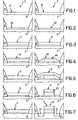
- Shown to an enlarged scale in the Figuresare vertical cross-sections through portions, not necessarily adjacent one another, of a semiconductor substrate wherein the memory devices are formed in accordance with the invention.
- the first step in the process of fabricating EPROM or Flash EPROM memory devicesconventionally comprises forming active areas 8 of all the active elements 3, such as floating gate MOS transistors 3b, of the matrix, and transistors 3a of the circuitry.
- the definition of the active areas 8, isolated from one another by insulating regions consisting of a field oxide 9,is carried out conventionally.
- a gate oxide layer 10may be grown for forming the transistors 3a, 3b.
- the unprotected polysilicon layer by the POLY1 maskis etched away.
- an intermediate dielectric layer 12e.g. of ONO (Oxide-Nitride-Oxide), is deposited.
- a second resist maskreferred to in the art as the MATRIX mask, is then used for masking the portion of the semiconductor where the memory matrix is to be formed.
- the first layer of polysilicon 11 and intermediate dielectric 12, being unprotected by the MATRIX mask,are etched away to expose the gate oxide layer 10 in the portion of the semiconductor where the circuitry is being formed.
- a second conductive layere.g. of polysilicon, is then deposited over the entire substrate.
- control electrodes 4b and word lines WL of the cell matrixwhich will drive the control electrodes of the memory cells in the same column are defined.
- a third resist maskreferred to in the art as the self-aligned etch mask and used for defining the second polysilicon layer 12, is then used for defining the word lines WL of the cell matrix.
- the second layer of polysilicon 5, unmasked by the self-aligned etch mask,is etched away by a conventional photolithographic step.
- a fourth maskreferred to in the art as the SAS mask.
- the residual field oxide layer between the word lines WLis etched away as shown in Figure 7, this being followed by an ion implantation step to form the source and drain regions 13.
- this dielectric layer 6could be of the TEOS type.
- the thickness of the dielectric layeris illustratively within the range of 500 ⁇ to 3000 ⁇ , enough to isolate the transistor gate electrodes 4 and the word lines of the matrix.
- a second dielectric layer 6ais deposited next to fill the gaps between the word lines of the matrix.
- This second dielectric layermay be a doped insulating oxide film of the BPSG type.
- this second dielectric layermay be deposited, by a HDPCVD (High Density Plasma Chemical Vapor Deposition) technique, or a SACVD (Sub-Atmospheric Chemical Vapor Deposition) technique.
- HDPCVDHigh Density Plasma Chemical Vapor Deposition
- SACVDSub-Atmospheric Chemical Vapor Deposition
- the inventive processprovides for a removal of the second dielectric layer 6b by a CMP (Chemical Mechanical Polishing) treatment to produce mechanically a planar surface.
- CMPChemical Mechanical Polishing
- This removal of second dielectric layercould also be achieved by a dry etch-back step.
- the etch-backis carried out to advantage using no additional masks, and is continued until the surface of the second polysilicon layer 5 of the word lines and the surface of the second polysilicon layer in the circuitry become exposed.
- the second dielectric layeris confined to just the gap regions between the word lines, and only the areas to be silicized are exposed.
- a transition metalsuch as titanium is deposited and then processed thermally to cause it to react selectively with the uncovered areas by the dielectric layer and produce a silicide layer 7.
- the process of this inventionallows the resistance of the conductive polysilicon layers to be reduced, and silicidation of the source and drain regions of the memory matrix avoided, thereby preventing any dangerous bridging by the silicide between the source/drain regions and the first polysilicon layer or the substrate surface in the active areas, which would impair the proper operation of the matrix, without introducing any additional masking steps in the process flow.
Landscapes
- Semiconductor Memories (AREA)
- Electrodes Of Semiconductors (AREA)
- Insulated Gate Type Field-Effect Transistor (AREA)
- Non-Volatile Memory (AREA)
Description
- matrices of memory cells, wherein each cell comprises afloating gate MOS transistor; and
- control circuitry comprising fast-logic MOS transistors.
- implanting source and drain regions of the transistor;
- depositing a transition metal;
- subjecting the transition metal to a thermal process forselectively reacting it with the substrate surface andproducing the silicide layer.
Claims (9)
- A selective silicidation process in the formation of non-volatileelectronic memory devices (1) integrated on a semiconductorsubstrate (2), said non-volatile memory devices (1)comprising a memory matrix and a circuitry, the memorymatrix comprising a plurality of active elements (3) formedwith gate (4) and drive (WL) regions, the process comprising thefollowing steps in the following order :forming active areas of said active elements (3),forming a gate oxide layer (10) on the semiconductorsubstrate (2),forming a first conducting layer (11) on said gateoxide layer (10),patterning the first conducting layer (11) with afirst resist mask,etching the first conducting layer (11) that isunprotected by the first resist mask to form floating gateelectrodes (4a) of the memory matrix,forming an intermediate dielectric layer (12) on theentire surface of the semiconductor substrate (2),masking the memory matrix with a second resist mask,etching the intermediate dielectric layer (12) and thefirst conducting layer (11) that is unprotected by thesecond resist mask,forming a polysilicon layer (5) on the entiresurface of the semiconductor substrate (2),patterning the polysilicon layer (5) with athird resist mask,etching the polysilicon layer (5) that isunprotected by the third resist mask to form control gateelectrodes (4b) and word lines of the memory cells,forming source and drain regions (13) of the memorycells,depositing a dielectric layer (6) on the entiresurface of the semiconductor substrate (2);removing said dielectric layer (6) to expose thepolysilicon layer (5);depositing a layer of a transition metal (7);subjecting the transition metal layer to a thermaltreatment for selectively reacting it with the polysiliconlayers and producing a silicide layer (8) on said controlgate electrodes (4b), said drive regions and said secondpolysilicon layer (5) in the circuitry.
- A selective silicidation process according to Claim 1,characterized in that the step of depositing saiddielectric layer (6) comprises a first step of depositing afirst dielectric layer of thickness enough to isolate thecontrol gate electrodes (4b) and a second step ofdepositing a second dielectric layer to fill the gapsbetween the word lines of the memory matrix.
- A selective silicidation process according to Claim 1,characterized in that before removing the third mask, afourth mask is deposited.
- A selective silicidation process according to Claim 1,characterized in that said removing step is a planarizingstep.
- A selective silicidation process according to Claim 4,characterized in that said planarizing step is carried outby CMP.
- A selective silicidation process according to Claim 4,characterized in that said planarizing step is carried outas a dry etch-back step.
- A selective silicidation process according to Claim 1,characterized in that the dielectric layer is TEOS.
- A selective silicidation process according to Claim 1,characterized in that the metal layer is titanium.
- A selective silicidation process according to Claim 2,characterized in that the first dielectric layer is TEOSand the second dielectric layer is BPSG.
Priority Applications (4)
| Application Number | Priority Date | Filing Date | Title |
|---|---|---|---|
| EP98830793AEP1017088B1 (en) | 1998-12-29 | 1998-12-29 | Selective silicidation process in non-volatile semiconductor memory devices |
| DE69832083TDE69832083D1 (en) | 1998-12-29 | 1998-12-29 | Selective silicidation process in nonvolatile semiconductor memories |
| JP11374714AJP2000200844A (en) | 1998-12-29 | 1999-12-28 | Selective silicidation method |
| US09/473,367US6602774B1 (en) | 1998-12-29 | 1999-12-28 | Selective salicidation process for electronic devices integrated in a semiconductor substrate |
Applications Claiming Priority (1)
| Application Number | Priority Date | Filing Date | Title |
|---|---|---|---|
| EP98830793AEP1017088B1 (en) | 1998-12-29 | 1998-12-29 | Selective silicidation process in non-volatile semiconductor memory devices |
Publications (2)
| Publication Number | Publication Date |
|---|---|
| EP1017088A1 EP1017088A1 (en) | 2000-07-05 |
| EP1017088B1true EP1017088B1 (en) | 2005-10-26 |
Family
ID=8236941
Family Applications (1)
| Application Number | Title | Priority Date | Filing Date |
|---|---|---|---|
| EP98830793AExpired - LifetimeEP1017088B1 (en) | 1998-12-29 | 1998-12-29 | Selective silicidation process in non-volatile semiconductor memory devices |
Country Status (4)
| Country | Link |
|---|---|
| US (1) | US6602774B1 (en) |
| EP (1) | EP1017088B1 (en) |
| JP (1) | JP2000200844A (en) |
| DE (1) | DE69832083D1 (en) |
Families Citing this family (4)
| Publication number | Priority date | Publication date | Assignee | Title |
|---|---|---|---|---|
| US6900507B1 (en)* | 2004-01-07 | 2005-05-31 | Micron Technology, Inc. | Apparatus with silicide on conductive structures |
| US7220643B1 (en)* | 2005-06-08 | 2007-05-22 | Spansion Llc | System and method for gate formation in a semiconductor device |
| US8129764B2 (en)* | 2008-06-11 | 2012-03-06 | Aptina Imaging Corporation | Imager devices having differing gate stack sidewall spacers, method for forming such imager devices, and systems including such imager devices |
| US8803243B2 (en) | 2012-01-03 | 2014-08-12 | International Business Machines Corporation | Complementary metal oxide semiconductor (CMOS) device having gate structures connected by a metal gate conductor |
Family Cites Families (12)
| Publication number | Priority date | Publication date | Assignee | Title |
|---|---|---|---|---|
| US4635347A (en)* | 1985-03-29 | 1987-01-13 | Advanced Micro Devices, Inc. | Method of fabricating titanium silicide gate electrodes and interconnections |
| JP2633555B2 (en)* | 1987-03-23 | 1997-07-23 | 株式会社東芝 | Method for manufacturing semiconductor device |
| US5470772A (en)* | 1991-11-06 | 1995-11-28 | Intel Corporation | Silicidation method for contactless EPROM related devices |
| US5780891A (en)* | 1994-12-05 | 1998-07-14 | Micron Technology, Inc. | Nonvolatile floating gate memory with improved interploy dielectric |
| US5654219A (en)* | 1996-02-07 | 1997-08-05 | Texas Instruments Incorporated | Annealed poly-silicide etch process |
| US5683941A (en)* | 1996-07-02 | 1997-11-04 | National Semiconductor Corporation | Self-aligned polycide process that utilizes a planarized layer of material to expose polysilicon structures to a subsequently deposited metal layer that is reacted to form the metal silicide |
| JPH1074915A (en)* | 1996-08-29 | 1998-03-17 | Sharp Corp | Nonvolatile semiconductor memory device |
| US6143613A (en)* | 1997-06-30 | 2000-11-07 | Vlsi Technology, Inc. | Selective exclusion of silicide formation to make polysilicon resistors |
| US5888870A (en)* | 1997-10-22 | 1999-03-30 | Advanced Micro Devices, Inc. | Memory cell fabrication employing an interpoly gate dielectric arranged upon a polished floating gate |
| US6133096A (en)* | 1998-12-10 | 2000-10-17 | Su; Hung-Der | Process for simultaneously fabricating a stack gate flash memory cell and salicided periphereral devices |
| US6136649A (en)* | 1999-10-12 | 2000-10-24 | Advanced Micro Devices, Inc. | Method for removing anti-reflective coating layer using plasma etch process after contact CMP |
| US6194258B1 (en)* | 2000-01-18 | 2001-02-27 | Taiwan Semiconductor Manufacturing Company | Method of forming an image sensor cell and a CMOS logic circuit device |
- 1998
- 1998-12-29DEDE69832083Tpatent/DE69832083D1/ennot_activeExpired - Lifetime
- 1998-12-29EPEP98830793Apatent/EP1017088B1/ennot_activeExpired - Lifetime
- 1999
- 1999-12-28USUS09/473,367patent/US6602774B1/ennot_activeExpired - Fee Related
- 1999-12-28JPJP11374714Apatent/JP2000200844A/ennot_activeWithdrawn
Also Published As
| Publication number | Publication date |
|---|---|
| DE69832083D1 (en) | 2005-12-01 |
| EP1017088A1 (en) | 2000-07-05 |
| US6602774B1 (en) | 2003-08-05 |
| JP2000200844A (en) | 2000-07-18 |
Similar Documents
| Publication | Publication Date | Title |
|---|---|---|
| US6074915A (en) | Method of making embedded flash memory with salicide and sac structure | |
| US6413821B1 (en) | Method of fabricating semiconductor device including nonvolatile memory and peripheral circuit | |
| US5696019A (en) | Self-aligned trench isolation for memory array using sidewall spacers | |
| US8541277B2 (en) | Non-volatile memory device and method for fabricating the same | |
| US5702964A (en) | Method for forming a semiconductor device having a floating gate | |
| US7005328B2 (en) | Non-volatile memory device | |
| US6271087B1 (en) | Method for forming self-aligned contacts and local interconnects using self-aligned local interconnects | |
| US6518124B1 (en) | Method of fabricating semiconductor device | |
| KR100518577B1 (en) | One time programmable memory device, integrated circuit including the same and method for fabricating thereof | |
| US6627491B2 (en) | Method of manufacturing non volatile memory device having two charge storage regions | |
| JPH04229654A (en) | Method for manufacture of contactless floating gate memory array | |
| US6211012B1 (en) | Method of fabricating an ETOX flash memory | |
| US6306713B1 (en) | Method for forming self-aligned contacts and local interconnects for salicided gates using a secondary spacer | |
| US6482699B1 (en) | Method for forming self-aligned contacts and local interconnects using decoupled local interconnect process | |
| US20070133289A1 (en) | NAND-type flash memory device with high voltage PMOS and embedded poly and methods of fabricating the same | |
| US5028553A (en) | Method of making fast, trench isolated, planar flash EEPROMS with silicided bitlines | |
| KR0146401B1 (en) | Method for manufacturing a semiconductor integrated circuit device having a stack gate structure | |
| US6451653B2 (en) | Manufacturing process for the integration in a semiconductor chip of an integrated circuit including a high-density integrated circuit components portion and a high-performance logic integrated circuit components portion | |
| US6380584B1 (en) | Semiconductor memory device with single and double sidewall spacers | |
| US6228715B1 (en) | Semiconductor memory device and method of manufacturing thereof | |
| EP1107309B1 (en) | Manufacturing process for non-volatile floating gate memory cells and control circuitry | |
| US6344386B1 (en) | Method for fabricating semiconductor device including memory cell region and CMOS logic region | |
| US20020096700A1 (en) | Non-volatile semiconductor memory device and method of manufacturing the same | |
| EP1017088B1 (en) | Selective silicidation process in non-volatile semiconductor memory devices | |
| US7115471B2 (en) | Method of manufacturing semiconductor device including nonvolatile memory |
Legal Events
| Date | Code | Title | Description |
|---|---|---|---|
| PUAI | Public reference made under article 153(3) epc to a published international application that has entered the european phase | Free format text:ORIGINAL CODE: 0009012 | |
| AK | Designated contracting states | Kind code of ref document:A1 Designated state(s):DE FR GB IT | |
| AX | Request for extension of the european patent | Free format text:AL;LT;LV;MK;RO;SI | |
| 17P | Request for examination filed | Effective date:20001228 | |
| AKX | Designation fees paid | Free format text:DE FR GB IT | |
| 17Q | First examination report despatched | Effective date:20040319 | |
| RTI1 | Title (correction) | Free format text:SELECTIVE SILICIDATION PROCESS IN NON-VOLATILE SEMICONDUCTOR MEMORY DEVICES | |
| GRAP | Despatch of communication of intention to grant a patent | Free format text:ORIGINAL CODE: EPIDOSNIGR1 | |
| GRAC | Information related to communication of intention to grant a patent modified | Free format text:ORIGINAL CODE: EPIDOSCIGR1 | |
| GRAS | Grant fee paid | Free format text:ORIGINAL CODE: EPIDOSNIGR3 | |
| GRAA | (expected) grant | Free format text:ORIGINAL CODE: 0009210 | |
| AK | Designated contracting states | Kind code of ref document:B1 Designated state(s):DE FR GB IT | |
| REG | Reference to a national code | Ref country code:GB Ref legal event code:FG4D | |
| REF | Corresponds to: | Ref document number:69832083 Country of ref document:DE Date of ref document:20051201 Kind code of ref document:P | |
| PG25 | Lapsed in a contracting state [announced via postgrant information from national office to epo] | Ref country code:DE Free format text:LAPSE BECAUSE OF FAILURE TO SUBMIT A TRANSLATION OF THE DESCRIPTION OR TO PAY THE FEE WITHIN THE PRESCRIBED TIME-LIMIT Effective date:20060127 | |
| PLBE | No opposition filed within time limit | Free format text:ORIGINAL CODE: 0009261 | |
| STAA | Information on the status of an ep patent application or granted ep patent | Free format text:STATUS: NO OPPOSITION FILED WITHIN TIME LIMIT | |
| 26N | No opposition filed | Effective date:20060727 | |
| EN | Fr: translation not filed | ||
| PG25 | Lapsed in a contracting state [announced via postgrant information from national office to epo] | Ref country code:FR Free format text:LAPSE BECAUSE OF FAILURE TO SUBMIT A TRANSLATION OF THE DESCRIPTION OR TO PAY THE FEE WITHIN THE PRESCRIBED TIME-LIMIT Effective date:20061215 | |
| PGFP | Annual fee paid to national office [announced via postgrant information from national office to epo] | Ref country code:IT Payment date:20071211 Year of fee payment:10 | |
| PG25 | Lapsed in a contracting state [announced via postgrant information from national office to epo] | Ref country code:FR Free format text:LAPSE BECAUSE OF FAILURE TO SUBMIT A TRANSLATION OF THE DESCRIPTION OR TO PAY THE FEE WITHIN THE PRESCRIBED TIME-LIMIT Effective date:20051231 | |
| PG25 | Lapsed in a contracting state [announced via postgrant information from national office to epo] | Ref country code:FR Free format text:LAPSE BECAUSE OF FAILURE TO SUBMIT A TRANSLATION OF THE DESCRIPTION OR TO PAY THE FEE WITHIN THE PRESCRIBED TIME-LIMIT Effective date:20051026 | |
| PGFP | Annual fee paid to national office [announced via postgrant information from national office to epo] | Ref country code:GB Payment date:20081125 Year of fee payment:11 | |
| GBPC | Gb: european patent ceased through non-payment of renewal fee | Effective date:20091229 | |
| PG25 | Lapsed in a contracting state [announced via postgrant information from national office to epo] | Ref country code:GB Free format text:LAPSE BECAUSE OF NON-PAYMENT OF DUE FEES Effective date:20091229 | |
| PG25 | Lapsed in a contracting state [announced via postgrant information from national office to epo] | Ref country code:IT Free format text:LAPSE BECAUSE OF NON-PAYMENT OF DUE FEES Effective date:20081229 |