EP1015669B1 - Electroplating method for forming a multilayer structure - Google Patents
Electroplating method for forming a multilayer structureDownload PDFInfo
- Publication number
- EP1015669B1 EP1015669B1EP98914464AEP98914464AEP1015669B1EP 1015669 B1EP1015669 B1EP 1015669B1EP 98914464 AEP98914464 AEP 98914464AEP 98914464 AEP98914464 AEP 98914464AEP 1015669 B1EP1015669 B1EP 1015669B1
- Authority
- EP
- European Patent Office
- Prior art keywords
- mask
- metal
- electroplating
- substrate
- layer
- Prior art date
- Legal status (The legal status is an assumption and is not a legal conclusion. Google has not performed a legal analysis and makes no representation as to the accuracy of the status listed.)
- Expired - Lifetime
Links
- 238000009713electroplatingMethods0.000titleclaimsabstractdescription195
- 238000000034methodMethods0.000titleclaimsabstractdescription184
- 239000000758substrateSubstances0.000claimsabstractdescription175
- 229910052751metalInorganic materials0.000claimsabstractdescription164
- 239000002184metalSubstances0.000claimsabstractdescription164
- 239000010410layerSubstances0.000claimsdescription160
- 150000002739metalsChemical class0.000claimsdescription22
- 229910003460diamondInorganic materials0.000claimsdescription8
- 239000010432diamondSubstances0.000claimsdescription8
- 239000002356single layerSubstances0.000claimsdescription3
- HBMJWWWQQXIZIP-UHFFFAOYSA-Nsilicon carbideChemical compound[Si+]#[C-]HBMJWWWQQXIZIP-UHFFFAOYSA-N0.000claimsdescription2
- 229910010271silicon carbideInorganic materials0.000claimsdescription2
- 230000000295complement effectEffects0.000abstractdescription5
- 229910021645metal ionInorganic materials0.000abstractdescription5
- 239000000203mixtureSubstances0.000description88
- 230000000873masking effectEffects0.000description73
- 238000007747platingMethods0.000description60
- 239000000463materialSubstances0.000description40
- 239000003792electrolyteSubstances0.000description38
- 239000007788liquidSubstances0.000description38
- 230000008569processEffects0.000description37
- 239000012528membraneSubstances0.000description36
- 239000011148porous materialSubstances0.000description24
- 238000005530etchingMethods0.000description23
- RYGMFSIKBFXOCR-UHFFFAOYSA-NCopperChemical compound[Cu]RYGMFSIKBFXOCR-UHFFFAOYSA-N0.000description22
- 229910052802copperInorganic materials0.000description22
- 239000010949copperSubstances0.000description22
- PXHVJJICTQNCMI-UHFFFAOYSA-NNickelChemical compound[Ni]PXHVJJICTQNCMI-UHFFFAOYSA-N0.000description21
- 238000010586diagramMethods0.000description21
- 238000004519manufacturing processMethods0.000description21
- 238000000151depositionMethods0.000description18
- 230000004888barrier functionEffects0.000description16
- 239000000945fillerSubstances0.000description16
- -1e.g.Substances0.000description15
- 229920002120photoresistant polymerPolymers0.000description14
- 238000000059patterningMethods0.000description13
- 235000012431wafersNutrition0.000description11
- 239000011248coating agentSubstances0.000description10
- 238000000576coating methodMethods0.000description10
- 150000002500ionsChemical class0.000description9
- 229910052759nickelInorganic materials0.000description9
- 239000007787solidSubstances0.000description9
- 239000007789gasSubstances0.000description8
- 238000003825pressingMethods0.000description8
- 239000000853adhesiveSubstances0.000description7
- 230000001070adhesive effectEffects0.000description7
- 238000002844meltingMethods0.000description7
- 230000008018meltingEffects0.000description7
- 239000000243solutionSubstances0.000description7
- 238000001914filtrationMethods0.000description6
- 239000012530fluidSubstances0.000description6
- 238000012545processingMethods0.000description6
- 238000009987spinningMethods0.000description6
- UFHFLCQGNIYNRP-UHFFFAOYSA-NHydrogenChemical compound[H][H]UFHFLCQGNIYNRP-UHFFFAOYSA-N0.000description5
- 229910052782aluminiumInorganic materials0.000description5
- XAGFODPZIPBFFR-UHFFFAOYSA-NaluminiumChemical compound[Al]XAGFODPZIPBFFR-UHFFFAOYSA-N0.000description5
- 230000015572biosynthetic processEffects0.000description5
- 239000000919ceramicSubstances0.000description5
- 238000004590computer programMethods0.000description5
- 230000008021depositionEffects0.000description5
- 238000004070electrodepositionMethods0.000description5
- 239000001257hydrogenSubstances0.000description5
- 229910052739hydrogenInorganic materials0.000description5
- 239000000843powderSubstances0.000description5
- 238000003860storageMethods0.000description5
- 239000000126substanceSubstances0.000description5
- 239000004642PolyimideSubstances0.000description4
- XUIMIQQOPSSXEZ-UHFFFAOYSA-NSiliconChemical compound[Si]XUIMIQQOPSSXEZ-UHFFFAOYSA-N0.000description4
- 239000000654additiveSubstances0.000description4
- 239000011159matrix materialSubstances0.000description4
- 239000002245particleSubstances0.000description4
- 229920001721polyimidePolymers0.000description4
- 229920001296polysiloxanePolymers0.000description4
- 229920001343polytetrafluoroethylenePolymers0.000description4
- 239000004810polytetrafluoroethyleneSubstances0.000description4
- 229910052710siliconInorganic materials0.000description4
- 239000010703siliconSubstances0.000description4
- 238000004544sputter depositionMethods0.000description4
- 239000004020conductorSubstances0.000description3
- 238000013461designMethods0.000description3
- 238000001312dry etchingMethods0.000description3
- 230000002209hydrophobic effectEffects0.000description3
- 238000007689inspectionMethods0.000description3
- 238000005459micromachiningMethods0.000description3
- 238000001020plasma etchingMethods0.000description3
- 229920000642polymerPolymers0.000description3
- 229920006395saturated elastomerPolymers0.000description3
- 239000004065semiconductorSubstances0.000description3
- 239000002002slurrySubstances0.000description3
- 238000004528spin coatingMethods0.000description3
- 239000002344surface layerSubstances0.000description3
- VHUUQVKOLVNVRT-UHFFFAOYSA-NAmmonium hydroxideChemical compound[NH4+].[OH-]VHUUQVKOLVNVRT-UHFFFAOYSA-N0.000description2
- 241000208967Polygala cruciataSpecies0.000description2
- 239000004743PolypropyleneSubstances0.000description2
- RTAQQCXQSZGOHL-UHFFFAOYSA-NTitaniumChemical compound[Ti]RTAQQCXQSZGOHL-UHFFFAOYSA-N0.000description2
- 239000000956alloySubstances0.000description2
- 229910045601alloyInorganic materials0.000description2
- 239000000908ammonium hydroxideSubstances0.000description2
- QVGXLLKOCUKJST-UHFFFAOYSA-Natomic oxygenChemical compound[O]QVGXLLKOCUKJST-UHFFFAOYSA-N0.000description2
- 238000004422calculation algorithmMethods0.000description2
- 238000004364calculation methodMethods0.000description2
- 239000003795chemical substances by applicationSubstances0.000description2
- 238000004140cleaningMethods0.000description2
- 150000001875compoundsChemical class0.000description2
- ARUVKPQLZAKDPS-UHFFFAOYSA-Lcopper(II) sulfateChemical compound[Cu+2].[O-][S+2]([O-])([O-])[O-]ARUVKPQLZAKDPS-UHFFFAOYSA-L0.000description2
- 125000004122cyclic groupChemical group0.000description2
- 239000008151electrolyte solutionSubstances0.000description2
- 230000006870functionEffects0.000description2
- 239000011521glassSubstances0.000description2
- 238000001746injection mouldingMethods0.000description2
- 239000004922lacquerSubstances0.000description2
- 239000006247magnetic powderSubstances0.000description2
- 230000013011matingEffects0.000description2
- 239000001301oxygenSubstances0.000description2
- 229910052760oxygenInorganic materials0.000description2
- 229920003229poly(methyl methacrylate)Polymers0.000description2
- 239000004926polymethyl methacrylateSubstances0.000description2
- 229920001155polypropylenePolymers0.000description2
- 238000002360preparation methodMethods0.000description2
- 238000007639printingMethods0.000description2
- 238000005086pumpingMethods0.000description2
- 238000005245sinteringMethods0.000description2
- 230000002269spontaneous effectEffects0.000description2
- 239000007921spraySubstances0.000description2
- 229920001169thermoplasticPolymers0.000description2
- 239000004416thermosoftening plasticSubstances0.000description2
- 239000010936titaniumSubstances0.000description2
- 229910052719titaniumInorganic materials0.000description2
- 238000002604ultrasonographyMethods0.000description2
- XLYOFNOQVPJJNP-UHFFFAOYSA-NwaterSubstancesOXLYOFNOQVPJJNP-UHFFFAOYSA-N0.000description2
- 239000001993waxSubstances0.000description2
- KWVGIHKZDCUPEU-UHFFFAOYSA-N2,2-dimethoxy-2-phenylacetophenoneChemical compoundC=1C=CC=CC=1C(OC)(OC)C(=O)C1=CC=CC=C1KWVGIHKZDCUPEU-UHFFFAOYSA-N0.000description1
- 229920002799BoPETPolymers0.000description1
- JPVYNHNXODAKFH-UHFFFAOYSA-NCu2+Chemical compound[Cu+2]JPVYNHNXODAKFH-UHFFFAOYSA-N0.000description1
- 239000002000Electrolyte additiveSubstances0.000description1
- 239000005041Mylar™Substances0.000description1
- CTQNGGLPUBDAKN-UHFFFAOYSA-NO-XyleneChemical compoundCC1=CC=CC=C1CCTQNGGLPUBDAKN-UHFFFAOYSA-N0.000description1
- 239000002033PVDF binderSubstances0.000description1
- 206010044038Tooth erosionDiseases0.000description1
- 238000002679ablationMethods0.000description1
- 239000003082abrasive agentSubstances0.000description1
- 239000002253acidSubstances0.000description1
- 239000002318adhesion promoterSubstances0.000description1
- 238000013019agitationMethods0.000description1
- 239000010405anode materialSubstances0.000description1
- 238000013459approachMethods0.000description1
- 230000000712assemblyEffects0.000description1
- 238000000429assemblyMethods0.000description1
- ABPRCTBWDBICPC-UHFFFAOYSA-Lazanium copper hydroxide sulfateChemical compoundS(=O)(=O)([O-])[O-].[Cu+2].[OH-].[NH4+]ABPRCTBWDBICPC-UHFFFAOYSA-L0.000description1
- 230000000903blocking effectEffects0.000description1
- 238000000071blow mouldingMethods0.000description1
- 238000003486chemical etchingMethods0.000description1
- 239000002131composite materialSubstances0.000description1
- 230000003750conditioning effectEffects0.000description1
- 238000011109contaminationMethods0.000description1
- 230000008602contractionEffects0.000description1
- 229910001431copper ionInorganic materials0.000description1
- 229910000365copper sulfateInorganic materials0.000description1
- 238000012937correctionMethods0.000description1
- 238000013500data storageMethods0.000description1
- 230000003247decreasing effectEffects0.000description1
- 238000005238degreasingMethods0.000description1
- 230000032798delaminationEffects0.000description1
- 238000004512die castingMethods0.000description1
- 239000004205dimethyl polysiloxaneSubstances0.000description1
- 238000006073displacement reactionMethods0.000description1
- 238000004090dissolutionMethods0.000description1
- 230000000694effectsEffects0.000description1
- 229920001971elastomerPolymers0.000description1
- 239000000806elastomerSubstances0.000description1
- 238000009760electrical discharge machiningMethods0.000description1
- 238000005516engineering processMethods0.000description1
- 230000001747exhibiting effectEffects0.000description1
- 238000011049fillingMethods0.000description1
- 238000011010flushing procedureMethods0.000description1
- 239000006260foamSubstances0.000description1
- 238000010100freeform fabricationMethods0.000description1
- 239000000499gelSubstances0.000description1
- 238000005247getteringMethods0.000description1
- 238000010438heat treatmentMethods0.000description1
- 238000007641inkjet printingMethods0.000description1
- 230000003993interactionEffects0.000description1
- 239000011229interlayerSubstances0.000description1
- 238000005495investment castingMethods0.000description1
- 238000005304joiningMethods0.000description1
- 238000010030laminatingMethods0.000description1
- 230000000670limiting effectEffects0.000description1
- 230000001050lubricating effectEffects0.000description1
- 238000003754machiningMethods0.000description1
- 230000014759maintenance of locationEffects0.000description1
- 230000007246mechanismEffects0.000description1
- 239000012229microporous materialSubstances0.000description1
- 238000002156mixingMethods0.000description1
- 239000012778molding materialSubstances0.000description1
- 238000012544monitoring processMethods0.000description1
- 238000000465mouldingMethods0.000description1
- 229910001453nickel ionInorganic materials0.000description1
- KERTUBUCQCSNJU-UHFFFAOYSA-Lnickel(2+);disulfamateChemical compound[Ni+2].NS([O-])(=O)=O.NS([O-])(=O)=OKERTUBUCQCSNJU-UHFFFAOYSA-L0.000description1
- 230000003287optical effectEffects0.000description1
- 238000002161passivationMethods0.000description1
- 230000035515penetrationEffects0.000description1
- 230000035699permeabilityEffects0.000description1
- 239000012782phase change materialSubstances0.000description1
- 239000004033plasticSubstances0.000description1
- 229920003023plasticPolymers0.000description1
- 229920000435poly(dimethylsiloxane)Polymers0.000description1
- 229920002981polyvinylidene fluoridePolymers0.000description1
- 238000011536re-platingMethods0.000description1
- 238000010107reaction injection mouldingMethods0.000description1
- 230000009467reductionEffects0.000description1
- 230000002829reductive effectEffects0.000description1
- 238000009877renderingMethods0.000description1
- 230000000717retained effectEffects0.000description1
- 230000000630rising effectEffects0.000description1
- 150000003839saltsChemical class0.000description1
- 238000005488sandblastingMethods0.000description1
- 238000009738saturatingMethods0.000description1
- 238000007650screen-printingMethods0.000description1
- 238000007789sealingMethods0.000description1
- 238000005204segregationMethods0.000description1
- 238000000926separation methodMethods0.000description1
- 238000007493shaping processMethods0.000description1
- 229920002379silicone rubberPolymers0.000description1
- 239000004945silicone rubberSubstances0.000description1
- UKLNMMHNWFDKNT-UHFFFAOYSA-Msodium chloriteChemical compound[Na+].[O-]Cl=OUKLNMMHNWFDKNT-UHFFFAOYSA-M0.000description1
- 229960002218sodium chloriteDrugs0.000description1
- 239000011343solid materialSubstances0.000description1
- 238000005507sprayingMethods0.000description1
- 238000000992sputter etchingMethods0.000description1
- 239000004094surface-active agentSubstances0.000description1
- 230000001360synchronised effectEffects0.000description1
- 238000003856thermoformingMethods0.000description1
- 238000012876topographyMethods0.000description1
- PISDRBMXQBSCIP-UHFFFAOYSA-Ntrichloro(3,3,4,4,5,5,6,6,7,7,8,8,8-tridecafluorooctyl)silaneChemical compoundFC(F)(F)C(F)(F)C(F)(F)C(F)(F)C(F)(F)C(F)(F)CC[Si](Cl)(Cl)ClPISDRBMXQBSCIP-UHFFFAOYSA-N0.000description1
- 238000009849vacuum degassingMethods0.000description1
- 238000007738vacuum evaporationMethods0.000description1
- 238000013022ventingMethods0.000description1
- 238000009736wettingMethods0.000description1
- 239000000080wetting agentSubstances0.000description1
- 238000004804windingMethods0.000description1
- 239000008096xyleneSubstances0.000description1
- NWONKYPBYAMBJT-UHFFFAOYSA-Lzinc sulfateChemical compound[Zn+2].[O-]S([O-])(=O)=ONWONKYPBYAMBJT-UHFFFAOYSA-L0.000description1
Images


Classifications
- C—CHEMISTRY; METALLURGY
- C25—ELECTROLYTIC OR ELECTROPHORETIC PROCESSES; APPARATUS THEREFOR
- C25D—PROCESSES FOR THE ELECTROLYTIC OR ELECTROPHORETIC PRODUCTION OF COATINGS; ELECTROFORMING; APPARATUS THEREFOR
- C25D5/00—Electroplating characterised by the process; Pretreatment or after-treatment of workpieces
- C25D5/02—Electroplating of selected surface areas
- B—PERFORMING OPERATIONS; TRANSPORTING
- B81—MICROSTRUCTURAL TECHNOLOGY
- B81C—PROCESSES OR APPARATUS SPECIALLY ADAPTED FOR THE MANUFACTURE OR TREATMENT OF MICROSTRUCTURAL DEVICES OR SYSTEMS
- B81C1/00—Manufacture or treatment of devices or systems in or on a substrate
- B81C1/00015—Manufacture or treatment of devices or systems in or on a substrate for manufacturing microsystems
- B81C1/00023—Manufacture or treatment of devices or systems in or on a substrate for manufacturing microsystems without movable or flexible elements
- B81C1/00126—Static structures not provided for in groups B81C1/00031 - B81C1/00119
- C—CHEMISTRY; METALLURGY
- C25—ELECTROLYTIC OR ELECTROPHORETIC PROCESSES; APPARATUS THEREFOR
- C25D—PROCESSES FOR THE ELECTROLYTIC OR ELECTROPHORETIC PRODUCTION OF COATINGS; ELECTROFORMING; APPARATUS THEREFOR
- C25D5/00—Electroplating characterised by the process; Pretreatment or after-treatment of workpieces
- C25D5/02—Electroplating of selected surface areas
- C25D5/022—Electroplating of selected surface areas using masking means
- B—PERFORMING OPERATIONS; TRANSPORTING
- B33—ADDITIVE MANUFACTURING TECHNOLOGY
- B33Y—ADDITIVE MANUFACTURING, i.e. MANUFACTURING OF THREE-DIMENSIONAL [3-D] OBJECTS BY ADDITIVE DEPOSITION, ADDITIVE AGGLOMERATION OR ADDITIVE LAYERING, e.g. BY 3-D PRINTING, STEREOLITHOGRAPHY OR SELECTIVE LASER SINTERING
- B33Y10/00—Processes of additive manufacturing
- C—CHEMISTRY; METALLURGY
- C25—ELECTROLYTIC OR ELECTROPHORETIC PROCESSES; APPARATUS THEREFOR
- C25D—PROCESSES FOR THE ELECTROLYTIC OR ELECTROPHORETIC PRODUCTION OF COATINGS; ELECTROFORMING; APPARATUS THEREFOR
- C25D1/00—Electroforming
- C—CHEMISTRY; METALLURGY
- C25—ELECTROLYTIC OR ELECTROPHORETIC PROCESSES; APPARATUS THEREFOR
- C25D—PROCESSES FOR THE ELECTROLYTIC OR ELECTROPHORETIC PRODUCTION OF COATINGS; ELECTROFORMING; APPARATUS THEREFOR
- C25D1/00—Electroforming
- C25D1/003—3D structures, e.g. superposed patterned layers
- C—CHEMISTRY; METALLURGY
- C25—ELECTROLYTIC OR ELECTROPHORETIC PROCESSES; APPARATUS THEREFOR
- C25D—PROCESSES FOR THE ELECTROLYTIC OR ELECTROPHORETIC PRODUCTION OF COATINGS; ELECTROFORMING; APPARATUS THEREFOR
- C25D17/00—Constructional parts, or assemblies thereof, of cells for electrolytic coating
- C25D17/06—Suspending or supporting devices for articles to be coated
- C—CHEMISTRY; METALLURGY
- C25—ELECTROLYTIC OR ELECTROPHORETIC PROCESSES; APPARATUS THEREFOR
- C25D—PROCESSES FOR THE ELECTROLYTIC OR ELECTROPHORETIC PRODUCTION OF COATINGS; ELECTROFORMING; APPARATUS THEREFOR
- C25D5/00—Electroplating characterised by the process; Pretreatment or after-treatment of workpieces
- C25D5/10—Electroplating with more than one layer of the same or of different metals
- C25D5/12—Electroplating with more than one layer of the same or of different metals at least one layer being of nickel or chromium
- C—CHEMISTRY; METALLURGY
- C25—ELECTROLYTIC OR ELECTROPHORETIC PROCESSES; APPARATUS THEREFOR
- C25D—PROCESSES FOR THE ELECTROLYTIC OR ELECTROPHORETIC PRODUCTION OF COATINGS; ELECTROFORMING; APPARATUS THEREFOR
- C25D5/00—Electroplating characterised by the process; Pretreatment or after-treatment of workpieces
- C25D5/22—Electroplating combined with mechanical treatment during the deposition
- C—CHEMISTRY; METALLURGY
- C25—ELECTROLYTIC OR ELECTROPHORETIC PROCESSES; APPARATUS THEREFOR
- C25D—PROCESSES FOR THE ELECTROLYTIC OR ELECTROPHORETIC PRODUCTION OF COATINGS; ELECTROFORMING; APPARATUS THEREFOR
- C25D5/00—Electroplating characterised by the process; Pretreatment or after-treatment of workpieces
- C25D5/60—Electroplating characterised by the structure or texture of the layers
- C25D5/605—Surface topography of the layers, e.g. rough, dendritic or nodular layers
- C25D5/611—Smooth layers
- H—ELECTRICITY
- H01—ELECTRIC ELEMENTS
- H01L—SEMICONDUCTOR DEVICES NOT COVERED BY CLASS H10
- H01L21/00—Processes or apparatus adapted for the manufacture or treatment of semiconductor or solid state devices or of parts thereof
- H01L21/02—Manufacture or treatment of semiconductor devices or of parts thereof
- H01L21/04—Manufacture or treatment of semiconductor devices or of parts thereof the devices having potential barriers, e.g. a PN junction, depletion layer or carrier concentration layer
- H01L21/18—Manufacture or treatment of semiconductor devices or of parts thereof the devices having potential barriers, e.g. a PN junction, depletion layer or carrier concentration layer the devices having semiconductor bodies comprising elements of Group IV of the Periodic Table or AIIIBV compounds with or without impurities, e.g. doping materials
- H01L21/28—Manufacture of electrodes on semiconductor bodies using processes or apparatus not provided for in groups H01L21/20 - H01L21/268
- H01L21/283—Deposition of conductive or insulating materials for electrodes conducting electric current
- H01L21/288—Deposition of conductive or insulating materials for electrodes conducting electric current from a liquid, e.g. electrolytic deposition
- H01L21/2885—Deposition of conductive or insulating materials for electrodes conducting electric current from a liquid, e.g. electrolytic deposition using an external electrical current, i.e. electro-deposition
- H—ELECTRICITY
- H05—ELECTRIC TECHNIQUES NOT OTHERWISE PROVIDED FOR
- H05K—PRINTED CIRCUITS; CASINGS OR CONSTRUCTIONAL DETAILS OF ELECTRIC APPARATUS; MANUFACTURE OF ASSEMBLAGES OF ELECTRICAL COMPONENTS
- H05K3/00—Apparatus or processes for manufacturing printed circuits
- H05K3/22—Secondary treatment of printed circuits
- H05K3/24—Reinforcing the conductive pattern
- H05K3/241—Reinforcing the conductive pattern characterised by the electroplating method; means therefor, e.g. baths or apparatus
- B—PERFORMING OPERATIONS; TRANSPORTING
- B81—MICROSTRUCTURAL TECHNOLOGY
- B81C—PROCESSES OR APPARATUS SPECIALLY ADAPTED FOR THE MANUFACTURE OR TREATMENT OF MICROSTRUCTURAL DEVICES OR SYSTEMS
- B81C2201/00—Manufacture or treatment of microstructural devices or systems
- B81C2201/01—Manufacture or treatment of microstructural devices or systems in or on a substrate
- B81C2201/0174—Manufacture or treatment of microstructural devices or systems in or on a substrate for making multi-layered devices, film deposition or growing
- B81C2201/0181—Physical Vapour Deposition [PVD], i.e. evaporation, sputtering, ion plating or plasma assisted deposition, ion cluster beam technology
- B—PERFORMING OPERATIONS; TRANSPORTING
- B81—MICROSTRUCTURAL TECHNOLOGY
- B81C—PROCESSES OR APPARATUS SPECIALLY ADAPTED FOR THE MANUFACTURE OR TREATMENT OF MICROSTRUCTURAL DEVICES OR SYSTEMS
- B81C2201/00—Manufacture or treatment of microstructural devices or systems
- B81C2201/01—Manufacture or treatment of microstructural devices or systems in or on a substrate
- B81C2201/0174—Manufacture or treatment of microstructural devices or systems in or on a substrate for making multi-layered devices, film deposition or growing
- B81C2201/0197—Processes for making multi-layered devices not provided for in groups B81C2201/0176 - B81C2201/0192
- B—PERFORMING OPERATIONS; TRANSPORTING
- B81—MICROSTRUCTURAL TECHNOLOGY
- B81C—PROCESSES OR APPARATUS SPECIALLY ADAPTED FOR THE MANUFACTURE OR TREATMENT OF MICROSTRUCTURAL DEVICES OR SYSTEMS
- B81C2201/00—Manufacture or treatment of microstructural devices or systems
- B81C2201/03—Processes for manufacturing substrate-free structures
- B81C2201/032—LIGA process
- Y—GENERAL TAGGING OF NEW TECHNOLOGICAL DEVELOPMENTS; GENERAL TAGGING OF CROSS-SECTIONAL TECHNOLOGIES SPANNING OVER SEVERAL SECTIONS OF THE IPC; TECHNICAL SUBJECTS COVERED BY FORMER USPC CROSS-REFERENCE ART COLLECTIONS [XRACs] AND DIGESTS
- Y10—TECHNICAL SUBJECTS COVERED BY FORMER USPC
- Y10T—TECHNICAL SUBJECTS COVERED BY FORMER US CLASSIFICATION
- Y10T428/00—Stock material or miscellaneous articles
- Y10T428/12—All metal or with adjacent metals
- Y10T428/12486—Laterally noncoextensive components [e.g., embedded, etc.]
- Y—GENERAL TAGGING OF NEW TECHNOLOGICAL DEVELOPMENTS; GENERAL TAGGING OF CROSS-SECTIONAL TECHNOLOGIES SPANNING OVER SEVERAL SECTIONS OF THE IPC; TECHNICAL SUBJECTS COVERED BY FORMER USPC CROSS-REFERENCE ART COLLECTIONS [XRACs] AND DIGESTS
- Y10—TECHNICAL SUBJECTS COVERED BY FORMER USPC
- Y10T—TECHNICAL SUBJECTS COVERED BY FORMER US CLASSIFICATION
- Y10T428/00—Stock material or miscellaneous articles
- Y10T428/23—Sheet including cover or casing
- Y10T428/239—Complete cover or casing
Definitions
- the inventionrelates to forming structures by electrochemical deposition.
- Microfabrication processesare being developed and refined for eventual application to the manufacture of complex devices including machines and instrumentation. These processes are being directed to the production of machines of miniaturized devices having features in the range of a few microns and in some cases submicron, some of which currently exist on a macroscopic scale.
- Microfabrication processesinclude: bulk micromachining, in which material is removed from regions of a substrate; surface micromachining, in which a thin conformal structural layer and one or more sacrificial layers are deposited onto a substrate; and LIGA, which generates 2.5-D extruded shapes by molding materials around metals electrodeposited within openings in thick synchrotron-processed photoresists. These processes are used to produce structures of simple geometries (e.g., they can be defined by 1-4 different cross sections), and are usually customized for each application.
- Solid freeform fabricationwhich is also referred to as rapid prototyping, is used to manufacture macroscopic parts from hundreds of layers by generating one layer at a time. These processes produce features typically greater than 50-100 um in width using layers typically greater than 50-150 um thick. These processes typically generate a layer serially. These processes employ structures for supporting the part being manufactured. The support structures are often customized to the part.
- US 5,605,614discloses a method of manufacturing by electrodeposition a magnetic microactuator which involves three subsequent electrodeposition steps using masks.
- US 5,209,817teaches a method of fabricating wiring and via connectors including the formation of a masking layer and an electrodeposition step.
- the present inventionis an electroplating method for forming a multilayer structure, the method comprising:
- the methodincludes electroplating a second metal from a second metal ion source onto the first substrate.
- the step of electroplating the second metalincludes: a) contacting the first substrate with a second article including a substrate and a conformable mask disposed in a pattern on the substrate; b) electroplating a second metal onto the first substrate in a second pattern, the second pattern corresponding to the complement of the conformable mask pattern of the second article; and c) removing the second article from the first substrate.
- the methodcan further include building additional layers.
- the inventionfeatures a method for manufacturing an element that includes forming a multi-layer structure by repeatedly forming layers according to the above-described electroplating methods.
- the electroplating methodsallow fabrication of devices from thin layers of materials such as, e.g., metals, polymers, ceramics, and semiconductor materials.
- the electroplating methodsproduce relatively homogeneous, isotropic elements (e.g., devices) without interlayer junctions.
- the electroplating methodscan be performed at low temperatures, thus allowing substrates such as integrated circuits and silicon wafers to be used as plating substrates.
- the electroplating methods of the inventioncan be used to fabricate devices of freeform geometry including high aspect ratio devices, hollow devices with internal features, devices with cantilevered and "chandelier" geometries, and functional assemblies of interconnected, stationary or moving parts (i.e., devices fabricated in an assembled state).
- the electroplating articles, apparatus, and methodsalso are particularly useful in mass production of devices.
- the inventionfeatures electroplating methods that enable the manufacture of elements having complex structures.
- the electroplating methodsinclude selective electroplating of layers that include both structural materials (e.g., metals) and support (i.e., sacrificial) materials; and subsequent removal (e.g., by etching, melting, or electrolytically dissolving) of the support materials.
- the structural material remaining after removal of the support materialdefines an element such as a microscopic or mesoscopic device.
- the electroplating methodsemploy electroplating articles that include a patterned conformable mask, optionally adhered to a support such as an electrode or a porous medium.
- the electroplating methodoccurs in an electroplating apparatus that includes an electroplating bath filled with electrolyte, an anode, and a cathode.
- the electrolytecontains metal ions and, optionally, other additives.
- the anodecan be part of the electroplating article, as described below, or can be located at a distance from the article.
- the substrate to be platedfunctions as the cathode unless otherwise specified.
- the materialsare referred to as metals and similar features are indicated with the same reference numerals.
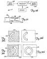
- electroplating articles 4include a patterned conformable mask 6 adhered to a support 8.
- the electroplating articlecan also be a patterned conformable mask.
- the supportcan be a porous medium (e.g., a filter), an anode, and combinations thereof.
- the articlecan include a plurality of different mask patterns on a single support. The different mask patterns can be contacted by a substrate in a predetermined sequence to sequentially plate a plurality of metal layers where each metal layer has a pattern corresponding to the complement of the mask pattern contacted, to form a multi-layered element.
- electroplating article 4can include one or more edge masks 3 on the outer surface of the article, for confining the metal being plated.
- a variety of methodscan be used to improve release of the mask from the substrate to be plated so as to prevent delamination of the mask from the support; gradually peeling the electroplating article (if flexible) off of the substrate with the aid of a dull blade; adding a non-stick/lubricating compound to the electrolyte; coating the mask surface with a non-stick composition (e.g., sputtered polytetrafluoroethylene); and vibration (e.g., ultrasound).
- a non-stick compositione.g., sputtered polytetrafluoroethylene
- vibratione.g., ultrasound
- the patterned conformable maskis sufficiently deformable (e.g., elastically deformable) to permit conformance of the mask to the surface of a substrate to be plated to maximize contact between the mask and the substrate, and to minimize (preferably eliminate) the presence of gaps between the mask and the substrate. Maximizing contact between the mask and the substrate minimizes the potential for flash formation.
- the maskis also sufficiently durable to enable repeated use (i.e., contacting with and removing from a substrate).
- the maskis sufficiently rigid and thin to prevent distortion of the mask features (i.e., the positive and negative features constituting the closed and open features of the mask pattern respectively) by the masking pressure.
- the maskpreferably is relatively thick compared to its peak and valley roughness and the curvature of the substrate to be plated.
- the maskpreferably exhibits very high volume electrical resistivity (e.g., 10 -14 Ohm-cm), has a very low permeability to ions in the electrolyte solution, and is chemically non-reactive with the plating electrolytes at the temperatures at which the plating operation is conducted.
- the maskcan be hydrophilic or hydrophobic, with hydrophilic being preferred. In the case of hydrophobic materials, relatively higher amounts of wetting agents can be included in the electrolyte to ensure wetting of the mask material.
- the maskpreferably is capable of forming a strong bond (e.g., a chemical or mechanical bond) to the support, such that small (e.g., 15x15 ⁇ m) isolated positive features are not delaminated by the mask fabrication process, normal handling of the mask or by removal of the mask material from the substrate to be plated.
- a strong bonde.g., a chemical or mechanical bond
- the patterned maskis preferably substantially planar and smooth to enable conformance to the substrate to be plated.
- the maskis capable of being patterned with negative and positive features of varying dimensions (e.g., 10-25 um or smaller, such as submicron), preferably with no mask residue blocking the negative features of the mask pattern.
- the pattern of the maskincludes apertures (i.e., negative features) extending through the mask thickness and defined by one or more side walls of the mask.
- the mask featurespreferably have a substantially planar wall profile and may have a slight wall angle (e.g., slightly divergent toward the substrate to be plated) re-contacting the mask to the substrate in the presence of an existing deposit.
- the maskcan be compound so as to include one or more layers of material, e.g., a relatively rigid layer (i.e., a high aspect ratio photoresist, e.g., SU-8 commercially available from MicroChem Corporation and synchrotron-processed polymethylmethacrylate), and a conformable layer.
- a relatively rigid layeri.e., a high aspect ratio photoresist, e.g., SU-8 commercially available from MicroChem Corporation and synchrotron-processed polymethylmethacrylate
- a conformable layere.g., a useful rigid layer.
- a positive photoresistsuch as Clariant AZ4620, which can be patterned by exposing it to ultraviolet light through the patterned conformable layer.
- Examples of useful masking compositionsinclude elastomers such as, e.g., polydimethylsiloxane (i.e., silicone rubber) commercially available, e.g., under the trade designation Sylgard from Dow-Corning (e.g., Sylgard 182 and 184), and under the trade designation RMS-033 from Gelest.
- the masking compositionscan include other additives, e.g., photoinitiators, fillers, and hydrogen getters.
- the porous mediumhas interconnected pores and is permeable to ions and additives present in electrolyte compositions.
- the porous mediumcan have one or more layers of varying porosity.
- the porous mediumpreferably has a pore size considerably finer than the minimum negative feature of the mask.
- the poresare preferably uniform in open area, e.g., the open area of any 20 ⁇ m square of the medium is consistent to 1%.
- Particularly useful porous mediumswhen used as filters, have a particle retention rating of 0.3-3 ⁇ m.
- each porous layercan vary in porosity and pore size, with the porous medium in closest proximity to the substrate to be plated exhibiting the above characteristics.
- the surfaces of the porous medium that contact the maskshould be sufficiently flat and smooth to ensure that the surface of the adhered mask that contacts the substrate to be plated is also flat and smooth.
- the porous mediumis chemically non-reactive with the electrolyte solution at the operating temperature of the electrolyte bath.
- Preferred porous mediumsare hydrophilic.
- the porous mediumpreferably is permeable to gas to allow venting of gas bubbles generated during the electroplating method.
- the porous mediumis free from shedding (i.e., does not release portions of itself into surrounding fluid), and is sufficiently durable so as to withstand multiple electroplating operations.
- suitable porous medium materialsinclude rigid, hydrophilic, slip cast ceramic disk porous mediums (commercially available from Coors Ceramics) and hydrophilized membrane porous mediums made from, e.g., polypropylene (commercially available under the trade designation GH from Gelman), polyvinylidenefluoride (commercially available under the trade designation Durapore from Millipore) and polytetrafluoroethylene (commercially available under the trade designation LCR from Millipore).
- Rigid porous mediumscan provide masking pressure when supported by their edges alone.
- Particularly useful highly permeable, porous mediumsinclude relatively thin, flexible, porous membranes.
- Porous membranescan be combined with a more rigid porous medium, which serves as a backing to provide the requisite pressure for masking applications.
- the porous membranecan be sandwiched between the more rigid porous medium and the mask and the porous medium can be used to supply the requisite masking pressure for the plating operation.
- the more rigid porous mediumcan have a relatively more coarse (i.e., larger) porosity than that useful for direct contact with the mask.
- Porous membranescan be integrated with the mask composition (or transformed into a mask).
- porous membranescan be installed in the drumhead fixture described below, or temporarily adhered to a rigid flat substrate (e.g., a silicone wafer, glass) with an adhesive composition (e.g., dry film photoresist). Porous membranes can be processed while adhered to the substrate and, after processing, removed by dissolving the adhesive.
- a rigid flat substratee.g., a silicone wafer, glass
- an adhesive compositione.g., dry film photoresist
- Masking pressurecan be applied to the porous membrane by the momentum of a stream or jet of electrolyte impinging on the membrane from behind, optionally in combination with dense particles incorporated into the electrolyte, and increasing the viscosity of the electrolyte, for example, by the addition of a polymer.
- Masking pressurecan also be applied to the membrane by sealing the membrane against the walls of the tank of the electroplating system and then pressurizing the electrolyte, causing the membrane to be pushed against the substrate to be plated.
- a dummy substratecan be used when the substrate to be plated is smaller than the porous medium to prevent the membrane from bulging.
- One example of an electroplating method that employs a porous membraneincludes pressing a relatively more rigid porous medium against the membrane, applying current, depositing a metal for a period, removing the current, withdrawing the rigid porous medium from contact with the membrane, slightly displacing the relatively more rigid porous medium in its own plane (e.g., in an orbital or linear fashion), and repeating the cycle. Displacing the relatively more rigid porous medium during each cycle allows a different portion of the rigid porous medium to make contact with the membrane.
- the mask/membraneseparates from the substrate to be plated while the relatively more rigid porous medium is separated from the membrane so as to allow exchange of fluids between the microvolume and bulk electrolyte.
- Another membrane plating methodincludes pressing a granular medium, tiny spheres, or rollers against the membrane using, e.g., a rigid screen.
- the tiny spheres and rollerscan be rotated in a pattern (e.g., a linear pattern using linear movement or a circular pattern using an orbital movement) on the membrane continuously or intermittently so as to average the local non-uniformities in pore structure of the rollers/spheres.
- the amplitude of movementis equal to (more preferably several times greater than) the diameter of the sphere or cylinder.
- the spheres/cylindersare relatively small and the membrane is relatively thick.
- the spheres/cylinderscan be made of the metal being plated.
- the electroplating articlecan consist of a patterned mask on an anode.
- the anodecan be soluble or insoluble, rigid or flexible, porous or nonporous, and can include an erodable layer (e.g., a metal layer) supported by a conductive material that does not erode (e.g., platinized titanium).
- the anodecan be of any dimension including a thin flexible sheet of metal.
- a soluble anodewill tend to erode during use.
- the anodecan be "redressed" periodically by reversing the polarity of the anode and plating metal back onto the anode through the negative features of the mask.
- the excess metalis supplied by the electrolyte in conjunction with another anode according to, e.g., through-mask plating processes used in electronics manufacturing.
- moving the anodewill prevent localized erosion of the anode.
- methods for forming electroplating articlesinclude applying a solid mask or liquid masking composition to a support, i.e., an anode, a porous medium and combinations thereof.
- the solid maskcan be patterned prior or subsequent to attachment to the support.
- Liquid masking compositionscan be patterned on a non-porous substrate (e.g., inert material, or a material that can be dissolved or melted (e.g., substrates of plastic, lacquer, or low melting point alloy)), cured (i.e., crosslinked, polymerized, hardened, solidified, gelled, and combinations thereof), and attached to a support or patterned and solidified directly on the support.
- anode surface preparation methodsinclude chemical microetching, lapping, sandblasting, and sintering a thin layer of powder onto the surface.
- a chemical adhesion promotere.g., Sylgard Prime Coat
- Sylgard Prime Coatcan also be used.
- a variety of methodscan be used to maintain or improve adhesion of the mask to a porous medium. These methods include melting the mask while pressing it into the porous medium resulting in a mechanical interlocking of the mask with the porosity of the porous medium, and applying an adhesive composition between the mask and the porous medium. Adhesion of the mask to the porous medium can also be enhanced by employing an adhesive that is a meltable material (e.g., glass), which can be dry deposited (e.g., sputtered) onto the surface of the patterned mask. When using an adhesive composition, it is preferable to employ methods that confine the adhesive composition to the areas located between the mask and the support (i.e., preventing the adhesive from bridging a negative feature that is only a few microns wide).
- a meltable materiale.g., glass
- Liquid masking compositionhas a tendency to soak into (i.e., uncontrollably absorb into) the pores of a porous medium.
- a variety of methodscan be employed to reduce "soak in" in regions of the porous medium that are to remain porous. Examples of suitable methods for preventing soak in include: supplying pressurized air to one side of the porous medium; treating the porous medium with a temporary filler composition that soaks in and fills the pores and then solidifies to form a barrier to penetration of the liquid masking composition; and treating the porous medium with a temporary filler composition that is immiscible with and denser than the liquid masking composition.
- the surface of the porous mediumcan be abraded after infiltrating the pores with filler composition to expose uncoated and unfilled surfaces allowing direct adhesion of the mask to the support.
- the filler compositioncan be dissolved or otherwise removed from the porous medium after the liquid masking composition has been cured to a solid.
- useful filler compositionsinclude acetone-soluble waxes and lacquers, soluble waxes used for investment casting cores, water soluble salts, gels, Crystal Bond 509, soluble thermoplastics, and phase-change materials (e.g., ice, electrorheological fluids).
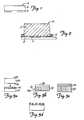
- one example of a method for rendering a porous medium temporarily nonporous using a filler compositionincludes: spinning a thin layer of a liquid filler composition 132 onto a relatively flat surface 131 (e.g., a silicon wafer) (preferably the thickness of the filler composition layer is adjusted so as to fill the pores of the porous medium to a predetermined height); contacting a first surface 136 of porous medium 130 to the spun-on filler composition 132 ( Fig. 3a ), allowing filler composition 132 to seep into the pores of the porous medium to a predetermined depth ( Fig.
- a relatively flat surface 131e.g., a silicon wafer
- liquid masking composition 134solidifies the filler composition 132; and applying (e.g., by spinning on) a sufficient amount of liquid masking composition 134 to a second surface 138 of the porous medium 130 opposite the first surface through which filler composition 132 entered the porous medium 130.
- Liquid masking composition 134is applied so as to produce a layer of masking composition of desired thickness on the surface of the porous medium. The remainder of the masking composition 134 can seep into the porous medium (for purposes of adhesion) only to the surface of the solidified filler 132.
- the methodfurther includes curing the masking composition 134; removing solidified filler 132; etching the negative features of the mask through the layer of porous medium 130 that is saturated with masking composition 134 to at least a depth at which the solidified filler 132 existed ( Fig. 3d ).
- Other methods for preventing or limiting soak ininclude restricting the volume of liquid masking composition that is applied to the porous medium to only a fraction of the pore volume in the porous medium causing the liquid to only partially fill the pores.
- One such methodincludes spraying a liquid masking composition onto the porous medium, while carefully controlling the flow rate and speed of the spray pattern.
- Another methodinvolves spin coating the liquid masking composition onto a non-absorbing sheet to obtain a uniform thin layer, and placing the porous medium in contact with the spun on liquid masking composition. When the porous medium is peeled away from the sheet or the sheet is dissolved or melted, a thin coating of masking composition is transferred to the porous medium (i.e., the masking composition remains adhered to the porous medium).
- the liquid masking compositioncan be cured prior to or subsequent to removal of the sheet.
- Another method for preventing soak ininvolves applying the liquid masking composition to a porous medium while the porous medium is spinning at high speed; the centrifugal forces spread the masking composition into a thin layer before it has had time to soak in excessively.
- barrier layerat or near the surface of the porous medium.
- the barrier layer(and optionally, some of the porous medium) is removed from the negative features of the mask, so as to expose the porosity of the porous medium.
- the regions of the barrier layer that will correspond to the positive features of the maskcan be removed prior to application of the mask.
- the barrier layercan be removed using various techniques including, e.g., chemical etching, dry etching, ion milling, laser machining, and melting (e.g., for thermoplastic based barriers).
- the barrier layercan also be formed by applying another material to the surface of the porous substrate, e.g., laminating a film of a solid material, such as dry film photoresist onto the porous medium; applying a liquid barrier layer, preferably of high viscosity, using one of the techniques discussed above that restrict soak-in volume; coating the porous medium with a thin layer of powder and melting the powder layer so as to form a non-porous coating; depositing a barrier film by vacuum evaporation, sputtering, CVD, or other process; and combinations thereof.
- another materiale.g., laminating a film of a solid material, such as dry film photoresist onto the porous medium
- a liquid barrier layerpreferably of high viscosity
- a porous anodeIn the case of a porous anode, soak in can be prevented using a variety of methods which include, applying a nonporous layer to the surface of the porous anode and, after patterning the mask, removing the nonporous layer in the negative areas of the mask to expose the anode; sintering a partly-compacted powder in a mold, patterning the mask, and immersing the structure in an etchant that attacks the metal of the anode, such that the outer non-porous layer of sintered anode material is dissolved (in the unmasked regions); melting the surface of the anode (e.g., by flame, or contact with a hot surface); temporarily filling the surface pores with a material, e.g., metal electrodeposited onto the porous surface; and by applying a nonporous barrier layer between the mask and the anode.
- a nonporous layerto the surface of the porous anode and, after patterning the mask, removing the non
- a method for forming an electroplating articleincludes forming a micromold 140 by coating (e.g., by spinning) a layer of resist 142 (e.g., photoresist commercially available under the trade designation SU-8 5 from MicroChem Corp.) onto a substrate 144 (e.g., a silicon wafer).
- a layer of photoresiste.g., photoresist commercially available under the trade designation SU-8 5 from MicroChem Corp.
- the layer of photoresisthas a thickness a few microns greater than that the desired thickness of the final mask.
- the photoresistcan be patterned using a photomask and, in the case of photopatternable resist compositions, a light source (e.g., a UV light source).
- the micromoldcan be made from a non-stick material such as, e.g., polytetrafluoroethylene or polypropylene, and can include a pattern formed, e.g., by reactive ion etching or excimer ablation, or micromolded from a master mold according to processes similar to processes used in the fabrication of compact discs.
- a non-stick materialsuch as, e.g., polytetrafluoroethylene or polypropylene
- the micromold surface including the photoresist and the substratecan be passivated by allowing the micromold to be exposed to vapors of, e.g., (tridecafluoro-1,1,2,2-tetrahydrooctyl)-1-trichlorosilane (commercially available from United Chemical Technologies).
- a liquid masking composition 146is then poured over the raised pattern defined by the patterned photoresist.
- Support 148is then pressed against micromold 140. Uniform pressure is applied such that liquid masking composition 148 is forced out of the area 150 located between the raised portions (i.e., positive features) of the resist pattern and the surface of support 148.
- liquid masking composition 146is completely squeezed out of the areas 150 corresponding to the positive features of resist 142.
- the entire assembly 152remains in this mating relationship until the liquid masking composition has cured.
- the assemblycan be transferred to an oven to cure.
- Any residual layer of masking composition remaining in negative features 158 of mask 156can be removed using dry etching (e.g., RIE with a mixture of O 2 and CF 4 gas), which may also reduce the thickness of the positive features of the mask.
- dry etchinge.g., RIE with a mixture of O 2 and CF 4 gas
- Uniform etching extending to the edge of the supportcan be accomplished by surrounding the support with a "dummy" substrate preferably of similar composition, such that non-uniformities due to edge effects are out of the area of interest.
- the etchmay be continued to remove any barrier layer present in the porous medium from the negative features of the mask and may be continued until a porous portion of the porous substrate is removed. If pores in a porous medium have been filled or are non-existent, the pores are re-established or established , e.g., by reactive ion etching.
- the methodincludes patterning a photoresist 142 onto a support 148 (i.e., the porous medium or the prepared anode) to the approximate thickness desired for the final mask.
- the areas of support 148 occupied by resist 142correspond to negative features of the mask through which metal can be deposited.
- the porous mediumcan be etched to remove the barrier layer from those areas of the porous medium that are not covered by resist.
- the methodfurther includes applying a liquid masking composition 146 to support 148, and optionally vacuum degassing the masking composition.
- a flat, smooth, non-stick (e.g., PTFE) sheet 160is then pressed against resist 142, and liquid masking composition 146 parallel to support 148, and pressure is applied to squeeze the liquid masking composition 146 out from between resist 142 and sheet 160.
- Masking composition 146is then cured, sheet 160 is removed, and residual masking composition overlaying the resist is removed, e.g., by etching (e.g., reactive ionization etching using a mixture of O 2 and CF 4 gas).
- Resist 142is then removed to expose areas of the support previously occupied by the resist.
- mask material that has seeped into the negative features of the mask from neighboring positive featurescan be removed by etching both mask and porous medium to the required depth. If pores of the porous medium have been filled or are non-existent, the pores can be established or re-established.
- another method for forming an electroplating articleincludes applying (e.g., by spinning on) a layer of photopatternable liquid masking composition 146, e.g., RMS-O33 (commercially available from Gelest) in combination with a photoinitiator (e.g., 2,2-dimethoxy-2-phenyl acetophenone (commercially available from Polysciences, Inc.)), to support 148.
- a layer of photopatternable liquid masking composition 146e.g., RMS-O33 (commercially available from Gelest) in combination with a photoinitiator (e.g., 2,2-dimethoxy-2-phenyl acetophenone (commercially available from Polysciences, Inc.)
- Liquid masking composition 146can be covered with a thin, oxygen-impermeable film (e.g., Mylar) to protect the composition from contact with oxygen.
- Masking composition 146is then exposed to patterned light (e.g., UV light transmitted through a photomask 162) to selectively cure the mask composition.
- patterned lighte.g., UV light transmitted through a photomask 162
- the filmis removed and the photopatternable masking composition is developed (e.g., by dissolving with xylene) removing uncured masking composition 146. If a nonporous barrier layer exists, it is removed (e.g., by dry etching) from the negative features of mask 156. Pores are established if necessary.
- the porous mediumcan be completely saturated with masking composition until there is a surface layer of masking composition having the desired thickness.
- the unexposed masking composition materialis dissolved in the developer.
- the porous mediumWhen patterning a porous medium, the porous medium can be tinted a dark shade or coated with an antireflection composition to reduce the amount of light scattered from the textured surface.
- the methodincludes applying a liquid masking composition 146 (or a solid mask) to support 148; curing liquid masking composition to form a solidified mask 156; coating mask 156 with either a thick resist 164 or a thin resist disposed on a thin metal layer (not shown); patterning resist 164 and, in the case of a metal layer, using the patterned resist to pattern the metal layer (e.g., by etching or lift-off); removing (e.g., wet etch, dry etch, or ion mill) mask 156 using thick resist 164 (and metal layer if present) as a mask; and in the case where the substrate is a porous medium, preferably removing the top layer of the porous medium to open pores; and removing, e.g., by stripping, the remaining resist 164 (and metal layer if used).
- a liquid masking composition 146or a solid mask
- a method for forming an electroplating articleincludes: applying a liquid masking composition 146 (or a solid mask) to support 148 to the desired thickness; curing (if liquid) the masking composition to form solidified mask 156; exposing solid mask 156 to patterned ultraviolet light of intensity and wavelength suitable for ablating the mask and support material, e.g., a UV excimer laser beam; ablating mask 156 until support 148 is exposed; and, when patterning a porous medium, ablating barrier layer 170 (if present) and, if necessary, the top layer of the porous medium to open pores.
- Methods similar to methods used in relief printingcan also be used to fabricate electroplating articles.
- One example of such a methodincludes: applying a liquid masking composition to a relief pattern, which might be produced by patterning a high aspect ratio photoresist such as AZ4620 or SU-8; pressing the relief pattern/masking composition structure against a support such that the masking composition adheres to the support; and removing the relief pattern.
- the formed electroplating articleincludes a support having a mask patterned with the inverse pattern of the relief pattern.
- Another example of such a methodincludes: creating a relief pattern on the support by etching of the support, or applying a durable photoresist, e.g., SU-8; coating a flat, smooth sheet with a thin, uniform layer of liquid masking composition; stamping the support/resist against the coated sheet (i.e., like a stamp and inkpad) to quickly mate and unmate the support/resist and the masking composition (preferably the support and the sheet are kept parallel); and curing the liquid masking composition.
- a durable photoresiste.g., SU-8
- coating a flat, smooth sheet with a thin, uniform layer of liquid masking compositioni.e., like a stamp and inkpad
- a method for forming an electroplating articlein which a surface layer of porous medium 148 is saturated with a liquid masking composition to the thickness of the desired mask.
- Liquid masking compositionis solidified producing a matrix 174 of solid mask 156 and porous medium 148.
- Matrix 174is then patterned, e.g., by etching or ablating selected areas of the matrix to a depth at least equal to the depth of the matrix "layer", to form electroplating article 176.
- the methodcan include saturating the entire porous medium with liquid masking composition, pattern curing the liquid masking composition, and removing the uncured masking composition.
- Other methods of forming electroplating articlesinclude, e.g., applying masking composition selectively to a support by such processes as screen printing, stencil printing and inkjet printing; and for porous mediums, melting a surface layer of the porous medium and forming negative features in the surface of the porous medium by etching/ablating through the melted layer to expose the pores of the porous medium and generate a relief pattern.
- the methods for forming electroplating articlescan also include etching the negative features (i.e., windows) of the mask pattern to increase the amount of relief on the electroplating article. In the case of a porous medium and a printed silicone mask, etching can be conducted by an oxygen plasma.
- the inventionfeatures electroplating methods that include contacting a substrate to be plated with an electroplating article of the invention; selectively electroplating a first metal, e.g., a support or sacrificial metal; and electroplating a second metal, e.g., a structural metal.
- the step of electroplating a second metalcan include selectively electroplating the second metal using an electroplating article of the present invention or blanket depositing the second metal.
- the electroplating methodcan be used to plate a single layer of metal or the method can be repeated such that additional metal is plated onto previously plated metal layers producing a multi-layered structure. After a predetermined number of layer(s) have been plated, at least a portion of the support metal can be removed, e.g., by etching.
- the structural metal that remainsdefines a microscopic or mesoscopic device.
- a method not forming part of the inventioncan also employ two electroplating articles to plate a single layer of one metal.
- a first metalis plated in a first pattern 230, the same metal is then plated in second pattern 232, to form plated metal layer 234.
- Second pattern 232may overlap first pattern 230.
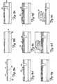
- the methodincludes contacting a substrate to be plated 2 with first article 4, which includes mask 6 and support 8, in the presence of a first metal ion source (i.e., electrolyte and anode 10), depositing a first metal 12, e.g., a sacrificial metal, contacting substrate 2 with a second article 14, which includes mask 16 and a support 18, depositing a second metal 20, e.g., a structural metal, in the presence of a second metal ion source (i.e., electrolyte and anode 22), optionally planarizing the layer, and repeating this method using differently patterned electroplating articles 4a, 4b, 14a, 14b to produce multi-layered structure 24, which, after etching all of sacrificial metal 12, becomes element 26.
- the second articlecan include a mask that has oversized positive features such that the surface area of one or more positive features of the mask extends beyond the corresponding surface area of the second metal ion source (i.e., electrolyte and
- the element formed during the electroplating methodcan remain attached to the substrate or can be removed from the substrate.
- One method for removing the elementincludes plating a first layer of support material onto the substrate such that etching removes the source of attachment of the element to the substrate.
- the electroplating methodincludes: contacting a substrate to be plated 2 with an electroplating article (not shown); selectively depositing a first metal 12 (i.e., either the structural or the support metal); blanket depositing a second metal 20 ( Fig. 12a ), and mechanically planarizing the deposited layer to achieve a flat, smooth layer of precise thickness ( Fig. 12b ).
- the planarized surfacecan be rinsed to remove abrasive particles present on the surface.
- the support metalis selectively plated and the structural metal is blanket deposited.
- planarization methodsinclude mechanical (e.g., diamond lapping and silicon carbide lapping), chemical-mechanical, and nonmechanical (e.g., electrical discharge machining), planarization processes.
- Diamond lappingis a particularly preferred planarization process. Diamond lapping can be performed using a single grade of diamond abrasive, e.g., about 1-6 micron, or diamond abrasives of various grades. Lapping with different grades of abrasive can be performed using separate lapping plates, or in different regions of a single plate. For example, a coarse diamond abrasive can be applied to the outer region of a spinning circular lapping plate, and a fine diamond abrasive can be applied to the inner region.
- a removable circular wallcan be provided between the inner and outer regions to increase segregation.
- the layer to be planarizedfirst contacts the outer region of the plate, is optionally rinsed to remove coarse abrasive, and then is moved to the inner region of the plate.
- the planarized surfacecan then be rinsed using a solution, e.g., water-based or electrolyte-based solution, to remove both abrasive and abraded particles from the planarized layer.
- the abrasive slurrypreferably is easily removable, e.g., water-soluble.
- Layer thickness, planarity and smoothnesscan be monitored, e.g., using an optical encoder, wear resistant stops, and by mating the layer under a known pressure with a precision flat metal plate and measuring the resistance across the plate-layer junction. Thickness of the plated metal can also be measured by contacting the plated metal with a mask having a pattern that is complementary to the plated metal pattern and measuring the displacement.
- One example of a preferred planarization processincludes allowing the work piece, i.e., the substrate having the layer to be planarized, to rotate within a "conditioning ring" on the lapping plate.
- Lappingcan also be performed by moving a workpiece around the surface of a lapping plate using the X/Y motion stages of the electroplating apparatus without rotating or releasing the workpiece. In this way, the tangential motion of the plate with respect to the substrate rotates through 360 degrees.
- the substrate to be platedcan include a conductive surface or a nonconductive surface provided with a conductive layer.
- the substrate to be platedcan be planar or nonplanar.
- the substrate to be platedcan also be a previously electroplated or deposited metal or a layer that includes at least one metal(s).
- the electroplating methodcan be performed, e.g., on an integrated circuit.
- One example of an electroplating method performed on an integrated circuitis shown in Fig. 13 .
- the aluminum padscan be connected to conductors that terminate at distant contact pads, which can be temporarily tied together by a bus. Referring to Fig.
- electroplating methodincludes: spin coating a layer of polyimide 34 onto thin copper disk 36; adhering copper disk 36 to bottom surface of silicon wafer 38, which includes aluminum pad 40, narrow conductor 42, contact pad 41, and passivation layer 44; partially sawing through wafer 38 to assist separation of the die after processing; spin coating photosensitive polyimide 35 on the top surface of wafer 38 to protect aluminum pads 40 and 41 during subsequent etching and to fill saw line 46; patterning polyimide to expose pads to be plated 40 and pads for electrical contact 41; degreasing wafer; immersing the structure in zincate plating solution; applying photoresist and patterning to create a bus; joining contact pads 41 by sputtering of copper to form a bus 48 that is in contact with pads 41 for the electroplating method; patterning resist over bus 48 to prevent nickel from depositing on bus 48; plating enough nickel 50 on aluminum pad 40 to allow planarization; removing the resist 35; making electrical contact with the plated metal; sputtering a planar base
- the electroplating methodscan employ cyclic plating to improve uniformity of the deposited metal layer.
- Cyclic platingincludes very briefly interrupting the current applied to the electrode in synchronization with removing the mask from the substrate to be plated, which simultaneously replenishes the electrolyte additives, vents any gases, and discharges particulates and broken-down additives from the microvolume defined by the support, the substrate to be plated, and the mask. Current is then re-applied in synchronization with contacting, i.e., remating, the mask with the substrate. This method can be repeated until the desired thickness of metal has been deposited.
- the walls of the maskcan be given a slight taper or draft (i.e., negative features defined by the mask are slightly larger on the side of the mask contacting the substrate), to facilitate repeated contact of a mask with a substrate in the presence of a deposit of incomplete thickness.
- Uniformity of the plated metal layercan be improved by controlling current density and adjusting current density on a feature-by-feature basis by controlling the local thickness, and optionally the local porosity, of the support of the electroplating article. Uniform plating can also be achieved by use as support an insoluble anode having a thin layer of a soluble coating having a thickness calculated to provide the desired thickness of plated metal on the substrate. Once the finite amount of ions in the volume of electrolyte within the area defined by the mask, the coating and the substrate are plated, plating ceases. As long as the coating is uniform in thickness, the plated metal will be uniform in thickness.
- Hydrogen bubble formationcan also be minimized by employing a low current density to increase current efficiency; decreasing temperature and/or pressurizing the electrolyte in bulk to increase the solubility of hydrogen in the electrolyte; employing a mask material that is impermeable to the electrolyte but gas permeable (e.g., a hydrophobic microporous material); performing the electroplating method under vacuum so that gas bubbles are pulled out of the mask features; employing antipitting agents (e.g., SNAP for nickel sulfamate electrolytes) to minimize the formation of pits by reducing the attachment of the gas bubbles to the substrate; increasing the masking pressure, which can locally increase electrolyte pressure due to reduced microvolume, which will establish large pressures on the electrolyte in localized areas keeping hydrogen in solution; and incorporating hydrogen gettering agent into the mask material (e.g., by mixing a fine powder into the liquid masking composition)
- a mask materialthat is impermeable to the electrolyte but gas
- etching compositions for selectively stripping copper from nickel structuresinclude: solutions of ammonium hydroxide and copper sulfate, solutions of ammonium hydroxide and sodium chlorite, with ammonium hydroxide-copper sulfate solution being preferred for etching structures attached to CMOS devices, and Enstripe C38 commercially available from Enthone OMI.
- Etchingcan also be performed in the presence of vibrations, e.g., ultrasound applied to the electrolyte or the substrate being plated, pressurized jets of etchant contacting the metal to be etched, and surfactant. Flash present on the structural metal, e.g., in the form of thin projections extending from the surface of the structural metal, can be removed, e.g., by acid etching or electropolishing.
- the electroplating methodescan be used to manufacture elements having complex microstructure and close tolerances between parts.
- One example of a method for manufacturing elements having parts that fit with close tolerances, e.g., gaps between the parts are between about 1-5um,involves electroplating the parts of the device in an unassembled, preferably pre-aligned, state. Once manufactured, the individual parts can be moved into operational relation with each other.
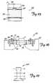
- a method of manufacturing device 188 including gear 190 and shaft 192 having retaining clips 200includes the electroplating methods disclosed above.
- Assembly fixture 194is plated in a pre-aligned location with gear 190.
- Chuck 196e.g., electromagnetic or vacuum
- etching gear 190may fall into contact with shaft 192.
- Chuck 196is then lowered, causing assembly fixture 194 to press gear 190 over retaining clips 200 on shaft 192 and into final position, as shown in Fig. 14c .
- Chuck 196is then raised removing assembly fixture 194 from the completed device 188, as shown in Figs. 14d-e .
- the electroplating methodcan also be used to manufacture elements in which at least a portion of the support metal is enclosed within the structural material such that the enclosed structural metal is not etched away during the removal process.
- a cross section of a plated element 236is shown in which support metal 238 remains encapsulated within structural metal 240 after support metal 238, that is accessible by etchant, is removed.
- the electroplating processescan also be used to manufacture tooling for molding (e.g., injection molding, metal injection molding, reaction injection molding, thermoforming, blow molding, and die casting). Mold inserts can be manufactured by orienting the two mold inserts so that the ejection axis of the part is parallel to the stacking axis of the layers and the parting surface of the part to be molded is the last layer deposited.
- the electroplating methodscan be used to form parts that include undercuts as shown in Fig. 16a , to form parts without draft as shown in Fig.
- the electroplating methodcan be performed in a variety of electroplating apparatus.
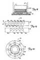
- One particularly useful apparatus for carrying out an electroplating methodis shown in Fig. 17 .
- Apparatus 56includes two baths 58, 60 (e.g., a nickel plating bath and a copper plating bath), and an inspection station 62.
- Each bath 58, 60is constructed to be capable of electroplating a different metal.
- Each bath 58, 60includes an electrolyte, an anode 59, 61, and an electroplating article 4, 14.
- apparatus 56accommodates a single substrate to be plated 2.
- the apparatuscan be constructed to accommodate multiple substrates to be plated and multiple electroplating articles.
- Each article 4, 14includes at least one patterned conformable mask 6,16 and is capable of depositing a pattern of metal.
- the mechanical and electrochemical control of the electroplating methodcan be controlled by computers.
- Substrate to be plated 2is transported by precision motion stages 64x, 64y, 64z, equipped with DC servo motors, stepper motors or combinations thereof, and precision encoders, between plating baths 58, 60 and rinsing station 66.
- Substrate 2 suspended on chuck 68enters first bath 58, positions itself over mask 6, contacts mask 6, and undergoes plating.
- substrate 2is removed from bath 58, rinsed and transferred to second plating bath 60 where it contacts a second mask 16, undergoes plating to a predetermined thickness (preferably the same thickness of the first deposited metal), is rinsed, and is returned to first bath 58.
- Inspection station 62including a high-resolution video microscope system with PC frame grabber, can be used in conjunction with control software to automatically record images of the deposited layers to a hard disk.
- apparatus 56is enclosed in a sealed chamber and equipped with a vacuum system to degas the mask.
- Useful mechanisms for applying controlled, uniform pressure to the substrateinclude applying a fluid pressure (e.g., through a pneumatic or hydraulic cylinder).
- a fluid pressuree.g., through a pneumatic or hydraulic cylinder.
- One particularly preferred method for applying uniform pressure across a circular substrateincludes applying pressure at the center of the substrate through a ball joint (e.g., a ball sandwiched between the cylinder or extension thereof and the substrate, possibly retained by a countersink in each).
- the ballallows the substrate to tilt as needed to conform to the mask surface and to find an equilibrium position within which pressure is uniformly distributed.
- the substratecan be held against the ball by surrounding the substrate with a tight-fitting flexible tube that is anchored at one end to the moving member.
- a very stiff, precision mechanical slide(e.g., a mechanical slide that incorporates crossed roller bearings) can be used to provide repeatable positioning of the mated substrate.
- the stages that move in the plane of the deposited layer, X/Y stages,can be fixed in location by clamps (e.g., an electromagnetic brake).
- the devicee.g., the chuck
- the devicethat carries the substrate to be plated can include a sliding insulating tube that moves into position as metal layers are added to the substrate.
- sliding insulating tube 67is shown in cross section in contact with edge mask 244 on support 14 and surrounding substrate 2 and plated metal layers 250.
- the electroplating apparatuscan be modified to include a device capable of directing a spray of electrolyte into the volume defined by the negative features of the article just prior to contacting the article to the substrate to be plated.
- the electroplating apparatuscan include a filtration system to control particulate contamination within the apparatus.
- the apparatuscan execute a self-cleaning cycle that includes pressurized rising, ultrasonic agitation, and filtration.
- the air within the apparatuscan be cleaned by a filtration system, e.g., a HEPA filtration system.
- the air and electrolyte filtration processescan operate continuously throughout the electroplating method.
- the electrolyte filtration systemcan be incorporated into a heating and pumping system to continuously circulate and warm the electrolyte to maintain homogeneous concentration and constant temperature.
- the thickness of the plated metal and plated metal layercan be controlled, e.g., by measuring the deposition rates of the metals and plating for a predetermined period; monitoring the integrated current, with adjustments for plating efficiency, normalizing for calculated mask area and calculating plating thickness; and through closed loop thickness control.
- the closed loop systemincludes inputing an estimate, based upon measured metal plating rates, into the software that controls the eletroplating method; plating a first metal to less than the desired thickness, pressing the substrate against a second electroplating article, such that the mask of the electroplating article contacts the first plated metal; forcing the substrate to move away from the support by an amount equal to the thickness of the plated layer; reading the thickness of the first plated metal using a high resolution (e.g., 0.1 um) encoder, linked to the substrate chuck; inputing this data into the software to update the stored rate value for the first metal; plating the remaining thickness of the first metal layer.
- This process and its complement for measuring the plating thickness of the second plated metalcan be repeated every few layers as a calibration.
- the position and orientation of the mask of the electroplating article with respect to the substrate and motion axes of the electroplating apparatuscan be determined by an alignment procedure that uses reserved areas on the substrate to be plated and at least two distantly separated masks, each bearing an alignment pattern.
- a thin layer of metalis plated onto the alignment pattern of the substrate, the rotational and translational misalignment of the mask with respect to the substrate is measured, e.g., using a video microscope, and corrections. Alignment accuracy can be verified by stripping the plated patterns and re-plating new patterns. Alignment can be repeated throughout the electroplating method as necessary.
- Another example of a useful alignment methodemploys a vernier pattern in which a pattern of fine lines having a first pitch is deposited over a second pattern of lines having a different pitch. The pitch spacing of the deposited pattern compared to the existing pattern provides an indication of the alignment error.
- a portion of another electroplating apparatus 66that includes bath 68 containing ions of a first metal, e.g., a nickel plating bath, bath 70 containing ions of a second metal, e.g., a copper plating bath, and multiple electroplating articles 72a-f and 74a-f, is shown.
- a first metale.g., a nickel plating bath
- bath 70containing ions of a second metal, e.g., a copper plating bath
- multiple electroplating articles 72a-f and 74a-fis shown.
- Each substrate to be plated 2enters apparatus 66 at the left end 76 of bath 68 contacts article 74a, becomes plated with first metal in the pattern of the mask of article 74a, transfers to bath 70 after rinse (not shown), contacts article 70a, becomes plated with a second metal in the pattern of the mask on article 70a, transfers to article 74b after rinse (not shown), in bath 68 and so on.
- substrate 2ahas received deposits of the first metal and the second metal for the first three layers of the microstructure and the first metal portion of the fourth layer.
- Substrate 2bis one layer behind substrate 2a
- substrate 2cis two layers behind wafer 2a, etc.
- the electroplating systemcan be arranged in an annular design in which the electroplating articles are arranged in rings and in which the individual electroplating articles are replaced after having contacted each of the substrates to be plated.
- Apparatus 78is designed to process 24 eight-inch diameter substrates 2.
- Apparatus 78is concentric in design and includes two outer rings 80, 82 and a central disk 84.
- Outer ring 80includes electrolyte bath 84 and electroplating articles (not shown) for selectively plating a first metal.
- Inner ring 82includes an electrolyte bath 86 for blanket-plating a second metal.
- Inner ring 82can include electroplating articles for selectively plating the second metal.
- Rotating lapping plate 85(if required), for planarizing the plated metal layers, is located at the center of apparatus 78. All processes (selective plating, blanket or selective plating and, optionally, planarization) occur during a single cycle, but on different substrates 2. At the end of the cycle, the substrates undergoing plating move in the pattern shown, in part, by arrows. Eight layers have been deposited after having completed all of the cycles in the system and arriving back at the starting point.
- the first plating articlePrior to the first substrate arriving back at the first plating article, the first plating article can be replaced by a new plating article. Likewise after the other plating articles have contacted each of the substrates they can be replaced, and substrates 2 can continue around apparatus 78, receiving as many layers as are required for the device being made. Rinsing stations are not shown but can be located in the spaces between the plating articles. Such an apparatus would permit the simultaneous manufacture about 2.5 million devices, each 500 microns square by 200 microns tall, in a 8 hour period.
- the electroplating apparatuscan also include a single bath containing ions of at least two metals (e.g., a Watts bath with added copper sulphate).
- a method for selectively depositing two metals from a common plating bath of their ionsis described in H. Yahalom and O. Zadok, "Formation of Compositionally Modulated Alloys by Electrodeposition," J. Material Sci., Vol. 22, p. 494 (1987 ).
- the plating bathincludes at least two electroplating articles, each of which is dedicated to plating one of the metals.
- the articlescan include a single mask pattern or multiple mask patterns in a side by side arrangement on the surface of the support.
- the substratecan contact the different mask patterns in a predetermined sequence, alternating with the mask pattern(s) on the second article, to build a three dimensional structure.
- an electroplating apparatus 88that includes a single bath 90 containing ions of two metals, e.g., nickel and copper ions, articles for plating the first metal 92, articles for plating the second metal 94, and substrates 2a-e, is shown.
- Each substrate 2enters apparatus 88 at the left end 96 of bath 90, contacts electroplating article 92a becomes plated with the first metal in the pattern of the mask of electroplating article 92a, transfers to and contacts article 94a, becomes plated with the second metal in the pattern of the mask on electroplating article 94a, transfers to electroplating article 92b, and so on.
- substrate 2ahas received deposits of the first metal and the second metal for the first three layers of the microstructure and the first metal portion of the fourth layer.
- Substrate 2bis one layer behind substrate 2a
- substrate 2cis two layers behind substrate 2a, and so on.
- a variety of methodscan be used to improve the copper deposition rate in a common bath electroplating system including, e.g., pulsing the plating current, increasing temperature (e.g., laser enhanced plating), pumping electrolyte through the support of the electroplating article, ultrasonic vibration, and increasing the copper content in the vicinity of the copper disk.
- One method for locally increasing the concentration of copperincludes galvanostatic dissolution of the copper anode while plating onto a dummy substrate.
- both nickel and copperare deposited onto the dummy substrate until sufficient copper to form a layer (about 1-2um thick) is generated in the electrolyte located between the anode and the substrate.
- the dummy substrateis substituted with the real substrate and the anode is replaced with a nickel anode. Copper is then deposited potentionstatically.
- Electroplating article holder 98Another method for locally increasing the concentration of copper includes employing a electroplating article holder 98 as shown in Fig. 22 .
- the volume of electroplating article holder 98contains copper rich electrolyte and is defined by side walls 100 of a cylinder, a porous support 102 having a conformable mask 104, and anode 106 (e.g., an insoluble platinized titanium anode).
- Electroplating article holder 98includes inlet and outlet ports for transferring electrolyte. This electroplating article holder can be immersed within a nickel plating bath, optionally separated by a barrier through which the substrate can intermittently pass.
- the substratepreferably is biased at a more positive potential than that at which copper reduction would occur until the substrate has contacted the copper electroplating article and current has been applied.
- the substratepreferably is again biased until the substrate is removed from the electrolyte, or applied to another article and current is again applied.
- Apparatus 260includes baths 262, 264 (e.g., a nickel plating bath and a copper plating bath), by an inspection station 266, and lapping station 268. Each bath 262, 264 is constructed to be capable of electroplating a different metal. Each bath 262, 264 includes an electrolyte and an anode 270, 272. Bath 264 also includes an electroplating article 274 for selectively depositing a first metal. Bath 262 is used for blanket depositing a second metal. Bath 262 includes a mask 276 for insulating the sides of element being fabricated on substrate 2 to prevent metal from plating on the sides of either one. Referring to Fig.
- Substrate 2includes a selectively deposited layer 278 and a blanket deposited layer 280.
- Electroplating article 108which is in contact with substrate to be plated 2, includes a relatively more rigid porous medium 110 having a relatively more coarse porosity, and relatively more thin, flexible porous membrane 112 having a relatively more fine porosity, and patterned mask 114 adhered to membrane 112. Patterned mask 114 is in contact with substrate 2 and anode 116 is disposed beyond porous medium 110. A metal deposit 118 is formed in the opening (i.e., a negative feature) defined by mask 114.
- FIG. 26another example of an electroplating apparatus 120 that employs a porous membrane 112 is shown.
- Porous membrane 112is mounted on drumhead 122 in a way that allows for handing and processing, maintains position of membrane 112 with respect to the substrate, and allows pressure to be exerted on porous membrane 112 through rigid porous medium 110 contacting porous membrane 112.
- Porous membrane 112is clamped between concentric O-rings 124, and pulled taut over a rigid porous medium, or, as shown, a cylindrical, hollow "barrel" 126 by tightening screws 128. If a barrel is used, rigid porous medium 110 is placed within barrel 126 so as to make contact with one side of membrane 112.
- Plating substrate 2contacts the other side of porous membrane 112.
- An intermediate compliant materiale.g., an open pore foam, may be disposed between porous membrane 112 and rigid porous medium 110 to provide a more uniform contact pressure between the mask and plating substrate 2.
- the methodemploys an automatic mask minimization algorithm for optimizing the number of masks for a given geometry.
- Application of the method to a valve like device 602, shown in Fig. 27can be described with reference to perforated lines A-D which indicate cross sections of the device 602.
- Cross sections B and Care identical and cross sections A and D are identical.
- a single maskcan be used for cross sections B and C and another mask can be used for cross sections A and D.
- the algorithmcompares the newly calculated cross sections with the previously calculated cross section for the same device or possibly those used to make the other devices and same metal.
- a new maskis generated if the difference between the two cross sections exceeds some predetermined (e.g., user specified) tolerance.
- the programalso generates an apparatus control file which directs the software that controls the electroplating apparatus such that masks are selected in a predetermined sequence corresponding to mask location within the electroplating apparatus and the layer being plated.
- the systemcan also export a layout file representing the first cross section of the part to be fabricated, allowing pad design for CMOS interfacing using a standard layout editor.
- the systemcan also display calculated cross sections to the user to allow error checking.
- Fig. 28is a functional block diagram of an exemplary computing system for calculation of cross sections of a three dimensional structure.
- system 610may include a processor 612, a memory 614 (e.g., a random access memory (RAM), and a program memory (for example, a writable read-only memory (ROM) such as a flash ROM)), input devices 616, and output devices 618.
- processor 612includes a central processing unit (CPU) that forms part of a general purpose computer, such as a PC, Macintosh, or workstation.
- CPUcentral processing unit
- Memory 614stores program code for execution by processor 612 including operating system code and application program code, and generally represents a magnetic hard drive or other storage device in combination with a random access memory accessed by processor 612. As one example, memory 614 could be realized in part by a storage drive contacting removable storage media carrying the application program code.
- Input devices 616include input media for entry of user input, such as a keyboard, mouse, and the like.
- Output devices 618include display devices including a view screen that provides graphic output, e.g., a CRT or flat panel monitor, a printer (e.g., a desk top printer, an inkjet printer, a laser printer, a photoplotter, and the like), the electroplating apparatus, a linotronic printer and the like.
- Fig. 29is a flow diagram illustrating a method for generating mask geometries and machine control parameters for fabrication of a three dimensional structure.
- processor 612receives and processes input corresponding to the three dimensional geometry of a structure to be cross sectioned from input devices 616 as indicated by block 622.
- Processor 612determines the extents in layer plane of the entire geometry of the three dimensional structure as indicated by block 623.
- Processor 612sets M, the number of layers (including one or more cross sections), equal to 1 and generates cross sections for the Mth layer, as indicated by block 624.
- Processor 612reads inputs relevant to each mask geometry including, e.g., scaling of the three dimensional geometry, layer thickness, mask dimensions, number of copies and spacing, and tolerance for mask minimization, as indicated by block 625.
- Processor 612creates the geometry of mask corresponding to the Mth layer, as indicated by block 616, writes the geometry of the cross section to a mask pattern file, indicated by blocks 628 and 630, and writes mask identification numbers for the Mth layer to a machine control file, as indicated by blocks 628 and 632.
- Memory 614stores mask pattern in the mask pattern file, as indicated at block 630.
- Memory 614stores location information in machine control file, as indicated at block 632.
- Processor 612queries if additional cross sections are needed to complete the geometry of the three dimensional structure, as indicated at block 634.
- processor 612increments M by 1 and generates a cross section for Mth layer as indicated at block 636.
- Processor 612creates a geometry of masks for Mth layer and sets N to zero, as indicated by blocks 638 and 640.
- Processor 612queries whether the geometry of the mask for the Mth layer is the same as or similar within a predetermined tolerance value to that of masks for the M-Nth layer, as indicated at blocks 642 and 646.
- processor 612replaces the mask geometry of the Mth layer with that of the M-Nth layer as indicated at block 648.
- Processor 612writes a mask identification number for the layer M to the machine control file (as indicated by blocks 650 and 652) and writes the mask geometry to the mask pattern file.
- processor 612queries whether M-N is greater than or equal to 1 as indicated at block 654.
- processor 612increments N by 1 and compares the geometry of mask for Mth layer with that of mask for M-Nth layer, as indicated at block 642. If processor 612 calculates that the geometry of the Mth layer has been compared to the geometry of each previous mask and no geometry matches, then processor 612 creates a geometry of the mask for the Mth layer, as indicated at block 656. Processor 612 then writes the geometry for the Mth layer to the mask pattern file (as indicated by block 658), sends an output to mask pattern file, as indicated by block 660, and writes mask identification number for the Mth layer to the machine control file (as indicated by blocks 650 and 652).
- Processor 612queries whether additional cross sections are required to be made of the three dimensional object (as indicated by block 634).
- processor 612increments M by 1 and continues the process again.
- Fig. 30is a flow diagram illustrating a method for electroplating a metal onto a substrate using patterned masks that represent a cross section slice of a three dimensional object.
- processor 612signals to the electroplating apparatus to perform machine initialization and sets M, the number of the layers plated equal to zero, as indicated at block 722.
- Processor 612increments M by 1 (as indicated by block 724), sets P (i.e., the number of different metals to be plated) equal to 1 and optionally biases the substrate to prevent spontaneous deposition of the metal (as indicated by block 726).
- Processor 612reads machine control file (indicated by block 730 to determine which layer is to be plated, and reads mask location file (indicated by block 732) to calculate the location of the mask pattern to be plated (indicated by block 728).
- Processor 612directs the electroplating apparatus to align the substrate to be plated with the mask for material P of layer M and to contact the substrate to the mask.
- Processor 612optionally measures layer thickness, if necessary, as indicated by block 734.
- Processor 612receives input that the substrate is in contact with the mask and turns off substrate bias (if turned on), as indicated by block 736.
- Processor 612instructs apparatus to deposit material P for layer M, as indicated by block 738.
- Processor 612receives input that layer has been deposited and applies a bias to the substrate, if required, as indicated at block 740.
- Processor 612instructs apparatus to remove the substrate from contact with the mask (as indicated at block 740), and to planarize layer M to predetermined thickness (if necessary), as indicated at block 744.
- Processorqueries whether P is greater than the number of metals of layer M, as indicated by block 746.
- processor 612increments P by 1 (as indicated by block 748), and drives the electroplating apparatus to align the substrate with a mask for P (i.e., Pi +1) metal of layer M, as indicated by block 728.
- processor 612drives electroplating apparatus to contact the substrate with the mask, and the above process is repeated until P is equal to the number of metals on layer M.
- processor 612queries whether M is the final layer (as indicated by block 750).
- processor 612ends the electroplating process as indicated by numeral 752.
- processor 612increments M by 1 as indicated by block 724, and processor 612 drives the electroplating process until the final layer has been plated.
- the data process and control processescan be implemented in digital electronic circuitry, or in computer hardware, firmware, software, or in combinations thereof.
- the data process and control processcan be implemented in a computer program product tangibly embodied in a machine-readable storage device for execution by a programmable processor; and method steps of the invention can be performed by a programmable processor executing a program of instructions to perform functions by operating on input data and generating output.
- the data processes and control processescan advantageously be implemented in one or more computer programs that are executable on a programmable system including at least one programmable processor coupled to receive data and instructions from, and to transmit data and instructions to, a data storage system, at least one input device, and at least one output device.
- Each computer programcan be implemented in a high-level procedural or object-oriented programming language, or in assembly or machine language if desired; and in any case, the language can be a compiled or interpreted language.
- Suitable processorsinclude, by way of example, both general and special purpose microprocessors. Generally, a processor will receive instructions and data from a read-only memory and/or a random access memory.
- Storage devices suitable for tangibly embodying computer program instructions and datainclude all forms of non-volatile memory, including by way of example semiconductor memory devices, such as EPROM, EEPROM, and flash memory devices; magnetic disks such as internal hard disks and removable disks; magneto-optical disks; and CD-ROM disks. Any of the foregoing can be supplemented by, or incorporated in, ASICs (application-specific integrated circuits).
- the data process and control processescan be implemented on a computer system having a display device such as a monitor or LCD screen for displaying information to the user and a keyboard and a pointing device such as a mouse or a trackball by which the user can provide input to the computer system.
- the computer systemcan be programmed to provide a graphical user interface through which computer programs interact with users.
- the substratecould be non-planar.
- the electroplating articlecan be sufficiently flexible to conform to the shape of the substrate surface, or shaped to match the surface.
- the electroplating articlecould be wrapped around a cylindrical substrate.
- Masking pressurecan be applied to nonplanar substrates through a powdered medium that conforms to the mask.
- electroplating methodeshave been described above with respect to two metals, a variety of materials, e.g., polymers, ceramics and semiconductor materials, and any number of metals can be deposited either by the electroplating methodes described above, or in separate processes that occur throughout the electroplating method.
- a thin plating basecan be deposited, e.g., by sputtering, over a deposit that is insufficiently conductive (e.g., an insulating layer) so as to enable continued electroplating.
- Multiple support materialscan be included in the electroplated element allowing selective removal of the support materials.
- electromagnetic motor 178including armature windings 180 connected to an integrated circuit at aluminum pads on substrate 182, can be formed by interrupting the electroplating method and etching a portion of the support metal (e.g., using a patterned resist) to produce cavity 184 (i.e., the rotor core of the motor) defined by structural metal 186 serving as an etch stop.
- Cavity 184is then filled with a magnetic powder (e.g., Ne-Fe-B), which is subsequently sintered and magnetized. If necessary, metal is sputtered onto the sintered magnetic powder to establish a plating base and the electroplating method can be resumed.
- Such cavitiescan be filled with solids, fluids or evacuated to form a vacuum.
- the metalscan be selectively deposited on the substrate by masking only the substrate.
- the metal being selectively plated onto the substrateis also deposited onto the previously deposited metals. After each of the metals for a given layer has been deposited, or more frequently, the layer is planarized to the desired thickness.
- the maskcan cover all of the previously deposited metals.
- the maskcan also be stepped in thickness to accommodate the topography of a partially plated substrate.
- Another embodiment of the electroplating methodinvolves manufacturing a structure well defined in shape and position according to the following method: preparing a piece of rigid, high strength material with an interconnected porosity (e.g., partly-sintered ceramic); shaping one surface of this piece such that it has the inverse (in the mold making sense) shape to that of the desired deposit; positioning the piece so that its surface lies opposite the substrate to be plated, at the desired position of the final deposit surface, and place an anode on the other side of it; plating metal onto the substrate while moving the piece (continuously or periodically) with sufficient force and in such a way that its surface still remains matched to that of the desired deposit (for a planar surface, move it within the plane, for a cylindrical surface, move it axially, etc.) (The movement can be a vibration sufficiently large to shear and remove any portion of the deposit that extends into the pores of the piece); continuing plating until the entire volume between the substrate and the piece is filled with the deposit, at which point the deposit will have molded itself to the shape of the
- Electroplating article 200includes a mask adhered to and coextensive with a patterned, rigid substrate (e.g., polymethylmethacrylate). During the electroplating method a deposit is formed in the window(s) (i.e., negative mask features) of the article. More specifically, substrate 204 is contacted with a first patterned electroplating article 200, as shown in Fig. 32a ; a first metal deposit 206 is formed in a shape defined by the pattern 202 in first electroplating article 200, first article 200 is then removed ( Fig. 32b ); substrate 204 is then contacted in alignment with a second patterned electroplating article 208 ( Fig.
- the electroplating articlescan include a region 210 of overlapping plated metal, which will have a corresponding greater thickness.
- the overlapping regioncan be planarized to create a planar layer of deposited metal.
- Masking pressurecan be applied by pressing an anode or porous medium against the electroplating article. The mask can be made stiffer by increasing its thickness.
Landscapes
- Chemical & Material Sciences (AREA)
- Engineering & Computer Science (AREA)
- Materials Engineering (AREA)
- Chemical Kinetics & Catalysis (AREA)
- Electrochemistry (AREA)
- Metallurgy (AREA)
- Organic Chemistry (AREA)
- Manufacturing & Machinery (AREA)
- Microelectronics & Electronic Packaging (AREA)
- Mechanical Engineering (AREA)
- Crystallography & Structural Chemistry (AREA)
- Analytical Chemistry (AREA)
- Physics & Mathematics (AREA)
- Condensed Matter Physics & Semiconductors (AREA)
- General Physics & Mathematics (AREA)
- Computer Hardware Design (AREA)
- Power Engineering (AREA)
- Electroplating Methods And Accessories (AREA)
- Micromachines (AREA)
- Ceramic Capacitors (AREA)
- Fixed Capacitors And Capacitor Manufacturing Machines (AREA)
- ing And Chemical Polishing (AREA)
Abstract
Description
- The invention relates to forming structures by electrochemical deposition.
- Microfabrication processes (also referred to as micromachining) are being developed and refined for eventual application to the manufacture of complex devices including machines and instrumentation. These processes are being directed to the production of machines of miniaturized devices having features in the range of a few microns and in some cases submicron, some of which currently exist on a macroscopic scale.
- Microfabrication processes include: bulk micromachining, in which material is removed from regions of a substrate; surface micromachining, in which a thin conformal structural layer and one or more sacrificial layers are deposited onto a substrate; and LIGA, which generates 2.5-D extruded shapes by molding materials around metals electrodeposited within openings in thick synchrotron-processed photoresists. These processes are used to produce structures of simple geometries (e.g., they can be defined by 1-4 different cross sections), and are usually customized for each application.
- Solid freeform fabrication, which is also referred to as rapid prototyping, is used to manufacture macroscopic parts from hundreds of layers by generating one layer at a time. These processes produce features typically greater than 50-100 um in width using layers typically greater than 50-150 um thick. These processes typically generate a layer serially. These processes employ structures for supporting the part being manufactured. The support structures are often customized to the part.
US 5,605,614 discloses a method of manufacturing by electrodeposition a magnetic microactuator which involves three subsequent electrodeposition steps using masks.US 5,209,817 teaches a method of fabricating wiring and via connectors including the formation of a masking layer and an electrodeposition step.- The present invention is an electroplating method for forming a multilayer structure, the method comprising:
- (a) forming a layer, comprising:
- (i) contacting a substrate to be plated with a conformable patterned mask;
- (ii) selectively electroplating a first metal onto the substrate using the conformable patterned mask;
- (iii) electroplating a second metal onto the substrate, wherein one of the metals is a support metal and the other is a structural metal;
- (b) repeating step (a) one or more times to form one or more additional layers onto one or more previously formed layers to form a multi-layered structure;
- (c) removing at least a portion of the support metal after a predetermined number of layers have been formed.
- The method includes electroplating a second metal from a second metal ion source onto the first substrate. In one embodiment, the step of electroplating the second metal includes: a) contacting the first substrate with a second article including a substrate and a conformable mask disposed in a pattern on the substrate; b) electroplating a second metal onto the first substrate in a second pattern, the second pattern corresponding to the complement of the conformable mask pattern of the second article; and c) removing the second article from the first substrate. The method can further include building additional layers.
- In another embodiment, the invention features a method for manufacturing an element that includes forming a multi-layer structure by repeatedly forming layers according to the above-described electroplating methods.
- The electroplating methods allow fabrication of devices from thin layers of materials such as, e.g., metals, polymers, ceramics, and semiconductor materials. The electroplating methods produce relatively homogeneous, isotropic elements (e.g., devices) without interlayer junctions. The electroplating methods can be performed at low temperatures, thus allowing substrates such as integrated circuits and silicon wafers to be used as plating substrates.
- The electroplating methods of the invention can be used to fabricate devices of freeform geometry including high aspect ratio devices, hollow devices with internal features, devices with cantilevered and "chandelier" geometries, and functional assemblies of interconnected, stationary or moving parts (i.e., devices fabricated in an assembled state). The electroplating articles, apparatus, and methods also are particularly useful in mass production of devices.
- Other features and advantages of the invention will be apparent from the following description of the preferred embodiments thereof, and from the claims.
Fig. 1 is view taken in cross section of an electroplating article ;Fig. 2 is a view taken in cross section of an electroplating article ;Fig. 3 is a diagram of a first embodiment of a method for forming an electroplating article;Fig. 4 is a diagram of a second embodiment of a method for forming an electroplating article;Fig. 5 is a diagram of a third embodiment of a method for forming an electroplating article;Fig. 6 is a diagram of a fourth embodiment of a method for forming an electroplating article;Fig. 7 is a diagram of a fifth embodiment of a method for forming an electroplating article;Fig. 8 is a diagram of a sixth embodiment of a method for forming an electroplating article;Fig. 9 is a diagram of a seventh embodiment of a method for forming an electroplating article;Fig. 10 is a diagram of a method for forming a deposit according to an electroplating method;Fig. 11 is a diagram of a method according to a first embodiment of the electroplating method of the invention;Fig. 12 is a diagram of a method according to a second embodiment of the electroplating method of the invention;Fig. 13 is a diagram of a method for fabricating an element on an integrated circuit;Fig. 14 is a diagram of a method for assembling elements fabricated together;Fig. 15 is a diagram of an element manufactured according to one embodiment of the electroplating method of the invention;Figs. 16a-d are views taken in cross section of elements manufactured according to one embodiment of the method of the invention;Fig. 17 is an electroplating apparatus ;Fig. 18 is a view taken in cross section of a substrate in contact with an electroplating article;Fig. 19 is a top view of a portion of an electroplating apparatus ;Fig. 20 is a top view of a portion of an electroplating apparatus ;Fig. 21 is a top view of a portion of an electroplating apparatus ;Fig. 22 is a view taken in cross section of one embodiment of an electroplating article holder ;Fig. 23 is a view taken in cross section of a second embodiment of an electroplating apparatus ;Fig. 24 is a highly enlarged view taken in cross section of a substrate in position in the electroplating apparatus ofFig. 23 ;Fig. 25 is a view taken in cross section of a third embodiment of a portion of an electroplating apparatus ;Fig. 26 is a view taken in cross section of another portion of the electroplating apparatus ofFig. 25 ;Fig. 27 is a diagram of a three dimensional object (shown in two dimensions) with cross section lines indicated;Fig. 28 is a functional block diagram of a computing system configured for calculation of cross sections of a three dimensional structure and for driving an electroplating apparatus;Fig. 29 is a flow diagram illustrating a method for generating mask pattern files and apparatus control files;Fig. 30 is a flow diagram illustrating a method for manufacturing a three dimensional object;Fig. 31 is a view taken in cross section of an electromagnetic motor;Fig. 32 is a diagram of an electroplating method employing more than one article- The invention features electroplating methods that enable the manufacture of elements having complex structures. The electroplating methods include selective electroplating of layers that include both structural materials (e.g., metals) and support (i.e., sacrificial) materials; and subsequent removal (e.g., by etching, melting, or electrolytically dissolving) of the support materials. The structural material remaining after removal of the support material defines an element such as a microscopic or mesoscopic device. The electroplating methods employ electroplating articles that include a patterned conformable mask, optionally adhered to a support such as an electrode or a porous medium.
- The electroplating method occurs in an electroplating apparatus that includes an electroplating bath filled with electrolyte, an anode, and a cathode. The electrolyte contains metal ions and, optionally, other additives. The anode can be part of the electroplating article, as described below, or can be located at a distance from the article. Throughout this application, the substrate to be plated functions as the cathode unless otherwise specified. To simplify the description, the materials are referred to as metals and similar features are indicated with the same reference numerals.
- Referring to
Fig. 1 ,electroplating articles 4 include a patternedconformable mask 6 adhered to asupport 8. The electroplating article can also be a patterned conformable mask. The support can be a porous medium (e.g., a filter), an anode, and combinations thereof. The article can include a plurality of different mask patterns on a single support. The different mask patterns can be contacted by a substrate in a predetermined sequence to sequentially plate a plurality of metal layers where each metal layer has a pattern corresponding to the complement of the mask pattern contacted, to form a multi-layered element. Referring toFig. 2 ,electroplating article 4 can include one ormore edge masks 3 on the outer surface of the article, for confining the metal being plated. - Contact between the electroplating article and the substrate to be plated is made by pressing the patterned mask against the substrate using a well-controlled, uniform pressure. The appropriate masking pressure will prevent flash (i.e., the deposition of metal in the area covered by the mask), and will prevent distortion of the features defined by the mask. When the electroplating article is removed from contact with the substrate, the mask remains adhered to the electroplating article.
- A variety of methods can be used to improve release of the mask from the substrate to be plated so as to prevent delamination of the mask from the support; gradually peeling the electroplating article (if flexible) off of the substrate with the aid of a dull blade; adding a non-stick/lubricating compound to the electrolyte; coating the mask surface with a non-stick composition (e.g., sputtered polytetrafluoroethylene); and vibration (e.g., ultrasound).
- The patterned conformable mask is sufficiently deformable (e.g., elastically deformable) to permit conformance of the mask to the surface of a substrate to be plated to maximize contact between the mask and the substrate, and to minimize (preferably eliminate) the presence of gaps between the mask and the substrate. Maximizing contact between the mask and the substrate minimizes the potential for flash formation. The mask is also sufficiently durable to enable repeated use (i.e., contacting with and removing from a substrate). The mask is sufficiently rigid and thin to prevent distortion of the mask features (i.e., the positive and negative features constituting the closed and open features of the mask pattern respectively) by the masking pressure. The mask preferably is relatively thick compared to its peak and valley roughness and the curvature of the substrate to be plated.
- The mask preferably exhibits very high volume electrical resistivity (e.g., 10-14 Ohm-cm), has a very low permeability to ions in the electrolyte solution, and is chemically non-reactive with the plating electrolytes at the temperatures at which the plating operation is conducted. The mask can be hydrophilic or hydrophobic, with hydrophilic being preferred. In the case of hydrophobic materials, relatively higher amounts of wetting agents can be included in the electrolyte to ensure wetting of the mask material.
- The mask preferably is capable of forming a strong bond (e.g., a chemical or mechanical bond) to the support, such that small (e.g., 15x15 µm) isolated positive features are not delaminated by the mask fabrication process, normal handling of the mask or by removal of the mask material from the substrate to be plated.
- The patterned mask is preferably substantially planar and smooth to enable conformance to the substrate to be plated. The mask is capable of being patterned with negative and positive features of varying dimensions (e.g., 10-25 um or smaller, such as submicron), preferably with no mask residue blocking the negative features of the mask pattern. The pattern of the mask includes apertures (i.e., negative features) extending through the mask thickness and defined by one or more side walls of the mask. The mask features preferably have a substantially planar wall profile and may have a slight wall angle (e.g., slightly divergent toward the substrate to be plated) re-contacting the mask to the substrate in the presence of an existing deposit.
- The mask can be compound so as to include one or more layers of material, e.g., a relatively rigid layer (i.e., a high aspect ratio photoresist, e.g., SU-8 commercially available from MicroChem Corporation and synchrotron-processed polymethylmethacrylate), and a conformable layer. Another example of a useful rigid layer is a positive photoresist such as Clariant AZ4620, which can be patterned by exposing it to ultraviolet light through the patterned conformable layer.
- Examples of useful masking compositions include elastomers such as, e.g., polydimethylsiloxane (i.e., silicone rubber) commercially available, e.g., under the trade designation Sylgard from Dow-Corning (e.g.,
Sylgard 182 and 184), and under the trade designation RMS-033 from Gelest. The masking compositions can include other additives, e.g., photoinitiators, fillers, and hydrogen getters. - The porous medium has interconnected pores and is permeable to ions and additives present in electrolyte compositions. The porous medium can have one or more layers of varying porosity. The porous medium preferably has a pore size considerably finer than the minimum negative feature of the mask. The pores are preferably uniform in open area, e.g., the open area of any 20 µm square of the medium is consistent to 1%. Particularly useful porous mediums, when used as filters, have a particle retention rating of 0.3-3µm. For those porous mediums that include multiple porous layers, each porous layer can vary in porosity and pore size, with the porous medium in closest proximity to the substrate to be plated exhibiting the above characteristics. The surfaces of the porous medium that contact the mask should be sufficiently flat and smooth to ensure that the surface of the adhered mask that contacts the substrate to be plated is also flat and smooth.
- The porous medium is chemically non-reactive with the electrolyte solution at the operating temperature of the electrolyte bath. Preferred porous mediums are hydrophilic. The porous medium preferably is permeable to gas to allow venting of gas bubbles generated during the electroplating method.
- Preferably the porous medium is free from shedding (i.e., does not release portions of itself into surrounding fluid), and is sufficiently durable so as to withstand multiple electroplating operations. Examples of suitable porous medium materials include rigid, hydrophilic, slip cast ceramic disk porous mediums (commercially available from Coors Ceramics) and hydrophilized membrane porous mediums made from, e.g., polypropylene (commercially available under the trade designation GH from Gelman), polyvinylidenefluoride (commercially available under the trade designation Durapore from Millipore) and polytetrafluoroethylene (commercially available under the trade designation LCR from Millipore). Rigid porous mediums can provide masking pressure when supported by their edges alone.
- Particularly useful highly permeable, porous mediums include relatively thin, flexible, porous membranes. Porous membranes can be combined with a more rigid porous medium, which serves as a backing to provide the requisite pressure for masking applications. The porous membrane can be sandwiched between the more rigid porous medium and the mask and the porous medium can be used to supply the requisite masking pressure for the plating operation. The more rigid porous medium can have a relatively more coarse (i.e., larger) porosity than that useful for direct contact with the mask. Porous membranes can be integrated with the mask composition (or transformed into a mask).
- To assist handling, porous membranes can be installed in the drumhead fixture described below, or temporarily adhered to a rigid flat substrate (e.g., a silicone wafer, glass) with an adhesive composition (e.g., dry film photoresist). Porous membranes can be processed while adhered to the substrate and, after processing, removed by dissolving the adhesive.
- Masking pressure can be applied to the porous membrane by the momentum of a stream or jet of electrolyte impinging on the membrane from behind, optionally in combination with dense particles incorporated into the electrolyte, and increasing the viscosity of the electrolyte, for example, by the addition of a polymer. Masking pressure can also be applied to the membrane by sealing the membrane against the walls of the tank of the electroplating system and then pressurizing the electrolyte, causing the membrane to be pushed against the substrate to be plated. A dummy substrate can be used when the substrate to be plated is smaller than the porous medium to prevent the membrane from bulging.
- One example of an electroplating method that employs a porous membrane includes pressing a relatively more rigid porous medium against the membrane, applying current, depositing a metal for a period, removing the current, withdrawing the rigid porous medium from contact with the membrane, slightly displacing the relatively more rigid porous medium in its own plane (e.g., in an orbital or linear fashion), and repeating the cycle. Displacing the relatively more rigid porous medium during each cycle allows a different portion of the rigid porous medium to make contact with the membrane. Preferably the mask/membrane separates from the substrate to be plated while the relatively more rigid porous medium is separated from the membrane so as to allow exchange of fluids between the microvolume and bulk electrolyte.
- Another membrane plating method includes pressing a granular medium, tiny spheres, or rollers against the membrane using, e.g., a rigid screen. The tiny spheres and rollers can be rotated in a pattern (e.g., a linear pattern using linear movement or a circular pattern using an orbital movement) on the membrane continuously or intermittently so as to average the local non-uniformities in pore structure of the rollers/spheres. Preferably the amplitude of movement is equal to (more preferably several times greater than) the diameter of the sphere or cylinder. Preferably the spheres/cylinders are relatively small and the membrane is relatively thick. The spheres/cylinders can be made of the metal being plated.
- The electroplating article can consist of a patterned mask on an anode. The anode can be soluble or insoluble, rigid or flexible, porous or nonporous, and can include an erodable layer (e.g., a metal layer) supported by a conductive material that does not erode (e.g., platinized titanium). The anode can be of any dimension including a thin flexible sheet of metal.
- A soluble anode will tend to erode during use. The anode can be "redressed" periodically by reversing the polarity of the anode and plating metal back onto the anode through the negative features of the mask. The excess metal is supplied by the electrolyte in conjunction with another anode according to, e.g., through-mask plating processes used in electronics manufacturing. For a system in which the mask is physically supported by and attached to a porous medium, and an anode is located directly behind the membrane, moving the anode will prevent localized erosion of the anode.
- In general, methods for forming electroplating articles include applying a solid mask or liquid masking composition to a support, i.e., an anode, a porous medium and combinations thereof. The solid mask can be patterned prior or subsequent to attachment to the support. Liquid masking compositions can be patterned on a non-porous substrate (e.g., inert material, or a material that can be dissolved or melted (e.g., substrates of plastic, lacquer, or low melting point alloy)), cured (i.e., crosslinked, polymerized, hardened, solidified, gelled, and combinations thereof), and attached to a support or patterned and solidified directly on the support.
- It is preferable to planarize the surface of the support that will receive the mask, so as to provide a smooth flat surface for receiving the mask. When applying the mask to an anode, it is preferable to first prepare the anode surface so as to maximize adhesion to the mask. Examples of useful anode surface preparation methods include chemical microetching, lapping, sandblasting, and sintering a thin layer of powder onto the surface. A chemical adhesion promoter (e.g., Sylgard Prime Coat) can also be used.
- A variety of methods can be used to maintain or improve adhesion of the mask to a porous medium. These methods include melting the mask while pressing it into the porous medium resulting in a mechanical interlocking of the mask with the porosity of the porous medium, and applying an adhesive composition between the mask and the porous medium. Adhesion of the mask to the porous medium can also be enhanced by employing an adhesive that is a meltable material (e.g., glass), which can be dry deposited (e.g., sputtered) onto the surface of the patterned mask. When using an adhesive composition, it is preferable to employ methods that confine the adhesive composition to the areas located between the mask and the support (i.e., preventing the adhesive from bridging a negative feature that is only a few microns wide).
- Liquid masking composition has a tendency to soak into (i.e., uncontrollably absorb into) the pores of a porous medium. A variety of methods can be employed to reduce "soak in" in regions of the porous medium that are to remain porous. Examples of suitable methods for preventing soak in include: supplying pressurized air to one side of the porous medium; treating the porous medium with a temporary filler composition that soaks in and fills the pores and then solidifies to form a barrier to penetration of the liquid masking composition; and treating the porous medium with a temporary filler composition that is immiscible with and denser than the liquid masking composition. The surface of the porous medium can be abraded after infiltrating the pores with filler composition to expose uncoated and unfilled surfaces allowing direct adhesion of the mask to the support. The filler composition can be dissolved or otherwise removed from the porous medium after the liquid masking composition has been cured to a solid.
- Examples of useful filler compositions include acetone-soluble waxes and lacquers, soluble waxes used for investment casting cores, water soluble salts, gels, Crystal Bond 509, soluble thermoplastics, and phase-change materials (e.g., ice, electrorheological fluids).
- Referring to
Fig. 3 , one example of a method for rendering a porous medium temporarily nonporous using a filler composition includes: spinning a thin layer of aliquid filler composition 132 onto a relatively flat surface 131 (e.g., a silicon wafer) (preferably the thickness of the filler composition layer is adjusted so as to fill the pores of the porous medium to a predetermined height); contacting afirst surface 136 of porous medium 130 to the spun-on filler composition 132 (Fig. 3a ), allowingfiller composition 132 to seep into the pores of the porous medium to a predetermined depth (Fig. 3b ); solidifying thefiller composition 132; and applying (e.g., by spinning on) a sufficient amount ofliquid masking composition 134 to asecond surface 138 of theporous medium 130 opposite the first surface through whichfiller composition 132 entered theporous medium 130.Liquid masking composition 134 is applied so as to produce a layer of masking composition of desired thickness on the surface of the porous medium. The remainder of the maskingcomposition 134 can seep into the porous medium (for purposes of adhesion) only to the surface of the solidifiedfiller 132. The method further includes curing the maskingcomposition 134; removing solidifiedfiller 132; etching the negative features of the mask through the layer of porous medium 130 that is saturated with maskingcomposition 134 to at least a depth at which the solidifiedfiller 132 existed (Fig. 3d ). - Other methods for preventing or limiting soak in include restricting the volume of liquid masking composition that is applied to the porous medium to only a fraction of the pore volume in the porous medium causing the liquid to only partially fill the pores. One such method includes spraying a liquid masking composition onto the porous medium, while carefully controlling the flow rate and speed of the spray pattern. Another method involves spin coating the liquid masking composition onto a non-absorbing sheet to obtain a uniform thin layer, and placing the porous medium in contact with the spun on liquid masking composition. When the porous medium is peeled away from the sheet or the sheet is dissolved or melted, a thin coating of masking composition is transferred to the porous medium (i.e., the masking composition remains adhered to the porous medium). The liquid masking composition can be cured prior to or subsequent to removal of the sheet.
- Another method for preventing soak in involves applying the liquid masking composition to a porous medium while the porous medium is spinning at high speed; the centrifugal forces spread the masking composition into a thin layer before it has had time to soak in excessively.
- Another approach to preventing soak in involves forming a barrier layer at or near the surface of the porous medium. After processing, the barrier layer (and optionally, some of the porous medium) is removed from the negative features of the mask, so as to expose the porosity of the porous medium. Optionally, to improve adhesion of the mask to the support, the regions of the barrier layer that will correspond to the positive features of the mask can be removed prior to application of the mask. The barrier layer can be removed using various techniques including, e.g., chemical etching, dry etching, ion milling, laser machining, and melting (e.g., for thermoplastic based barriers). The barrier layer can also be formed by applying another material to the surface of the porous substrate, e.g., laminating a film of a solid material, such as dry film photoresist onto the porous medium; applying a liquid barrier layer, preferably of high viscosity, using one of the techniques discussed above that restrict soak-in volume; coating the porous medium with a thin layer of powder and melting the powder layer so as to form a non-porous coating; depositing a barrier film by vacuum evaporation, sputtering, CVD, or other process; and combinations thereof.
- In the case of a porous anode, soak in can be prevented using a variety of methods which include, applying a nonporous layer to the surface of the porous anode and, after patterning the mask, removing the nonporous layer in the negative areas of the mask to expose the anode; sintering a partly-compacted powder in a mold, patterning the mask, and immersing the structure in an etchant that attacks the metal of the anode, such that the outer non-porous layer of sintered anode material is dissolved (in the unmasked regions); melting the surface of the anode (e.g., by flame, or contact with a hot surface); temporarily filling the surface pores with a material, e.g., metal electrodeposited onto the porous surface; and by applying a nonporous barrier layer between the mask and the anode.
- A variety of methods can be used to pattern the electroplating article. Referring to
Fig. 4 , a method for forming an electroplating article is shown. The method includes forming amicromold 140 by coating (e.g., by spinning) a layer of resist 142 (e.g., photoresist commercially available under the trade designation SU-8 5 from MicroChem Corp.) onto a substrate 144 (e.g., a silicon wafer). Preferably the layer of photoresist has a thickness a few microns greater than that the desired thickness of the final mask. The photoresist can be patterned using a photomask and, in the case of photopatternable resist compositions, a light source (e.g., a UV light source). A positive feature of the resist corresponds to a negative feature of the mask. Optionally, the micromold can be made from a non-stick material such as, e.g., polytetrafluoroethylene or polypropylene, and can include a pattern formed, e.g., by reactive ion etching or excimer ablation, or micromolded from a master mold according to processes similar to processes used in the fabrication of compact discs. - The micromold surface including the photoresist and the substrate can be passivated by allowing the micromold to be exposed to vapors of, e.g., (tridecafluoro-1,1,2,2-tetrahydrooctyl)-1-trichlorosilane (commercially available from United Chemical Technologies). A
liquid masking composition 146 is then poured over the raised pattern defined by the patterned photoresist.Support 148 is then pressed againstmicromold 140. Uniform pressure is applied such thatliquid masking composition 148 is forced out of thearea 150 located between the raised portions (i.e., positive features) of the resist pattern and the surface ofsupport 148. Preferably,liquid masking composition 146 is completely squeezed out of theareas 150 corresponding to the positive features of resist 142. Theentire assembly 152 remains in this mating relationship until the liquid masking composition has cured. For a heat-curable masking composition, the assembly can be transferred to an oven to cure. - After cure,
excess mask material 154 surroundingsupport 148 is removed. In the case of a mask that has been cured in the oven, the assembly is quickly disassembled to minimize differential thermal contraction between support and the mold. The support and curedmask 156 is pulled away frommold 140 such that curedmask 156 detaches frommicromold 140, yet remains adhered to support 148. Mask 156 exhibits a pattern inverse to that ofmicromold 140.Micromold 140 can be reused. If necessary,micromold 140 can be cleaned to remove mask residue. One example of a useful silicone cleaning composition is a silicone stripper, e.g., Amtex CCR (commercially available from Amtex Chemical Corp.). - Any residual layer of masking composition remaining in
negative features 158 ofmask 156 can be removed using dry etching (e.g., RIE with a mixture of O2 and CF4 gas), which may also reduce the thickness of the positive features of the mask. Uniform etching extending to the edge of the support can be accomplished by surrounding the support with a "dummy" substrate preferably of similar composition, such that non-uniformities due to edge effects are out of the area of interest. - When the mask is adhered to a porous medium, the etch may be continued to remove any barrier layer present in the porous medium from the negative features of the mask and may be continued until a porous portion of the porous substrate is removed. If pores in a porous medium have been filled or are non-existent, the pores are re-established or established , e.g., by reactive ion etching.
- Another method for forming an electroplating article is shown in
Fig. 5 . The method includes patterning aphotoresist 142 onto a support 148 (i.e., the porous medium or the prepared anode) to the approximate thickness desired for the final mask. The areas ofsupport 148 occupied by resist 142 correspond to negative features of the mask through which metal can be deposited. When patterning a porous medium that includes a barrier, the porous medium can be etched to remove the barrier layer from those areas of the porous medium that are not covered by resist. The method further includes applying aliquid masking composition 146 to support 148, and optionally vacuum degassing the masking composition. A flat, smooth, non-stick (e.g., PTFE)sheet 160 is then pressed against resist 142, andliquid masking composition 146 parallel to support 148, and pressure is applied to squeeze theliquid masking composition 146 out from between resist 142 andsheet 160. Maskingcomposition 146 is then cured,sheet 160 is removed, and residual masking composition overlaying the resist is removed, e.g., by etching (e.g., reactive ionization etching using a mixture of O2 and CF4 gas). Resist 142 is then removed to expose areas of the support previously occupied by the resist. When patterning a porous medium, mask material that has seeped into the negative features of the mask from neighboring positive features can be removed by etching both mask and porous medium to the required depth. If pores of the porous medium have been filled or are non-existent, the pores can be established or re-established. - Referring to
Fig. 6 , another method for forming an electroplating article includes applying (e.g., by spinning on) a layer of photopatternableliquid masking composition 146, e.g., RMS-O33 (commercially available from Gelest) in combination with a photoinitiator (e.g., 2,2-dimethoxy-2-phenyl acetophenone (commercially available from Polysciences, Inc.)), to support 148.Liquid masking composition 146 can be covered with a thin, oxygen-impermeable film (e.g., Mylar) to protect the composition from contact with oxygen. Maskingcomposition 146 is then exposed to patterned light (e.g., UV light transmitted through a photomask 162) to selectively cure the mask composition. The film is removed and the photopatternable masking composition is developed (e.g., by dissolving with xylene) removinguncured masking composition 146. If a nonporous barrier layer exists, it is removed (e.g., by dry etching) from the negative features ofmask 156. Pores are established if necessary. For those photopatternable masking compositions that are negative working the porous medium can be completely saturated with masking composition until there is a surface layer of masking composition having the desired thickness. After photopatterning, the unexposed masking composition material (including that in the pores) is dissolved in the developer. - When patterning a porous medium, the porous medium can be tinted a dark shade or coated with an antireflection composition to reduce the amount of light scattered from the textured surface.
- Referring to
Fig. 7 , another method for making an electroplating article is shown. The method includes applying a liquid masking composition 146 (or a solid mask) to support 148; curing liquid masking composition to form a solidifiedmask 156; coatingmask 156 with either a thick resist 164 or a thin resist disposed on a thin metal layer (not shown); patterning resist 164 and, in the case of a metal layer, using the patterned resist to pattern the metal layer (e.g., by etching or lift-off); removing (e.g., wet etch, dry etch, or ion mill)mask 156 using thick resist 164 (and metal layer if present) as a mask; and in the case where the substrate is a porous medium, preferably removing the top layer of the porous medium to open pores; and removing, e.g., by stripping, the remaining resist 164 (and metal layer if used). - Referring to
Fig. 8 , a method for forming an electroplating article is shown which includes: applying a liquid masking composition 146 (or a solid mask) to support 148 to the desired thickness; curing (if liquid) the masking composition to form solidifiedmask 156; exposingsolid mask 156 to patterned ultraviolet light of intensity and wavelength suitable for ablating the mask and support material, e.g., a UV excimer laser beam; ablatingmask 156 untilsupport 148 is exposed; and, when patterning a porous medium, ablating barrier layer 170 (if present) and, if necessary, the top layer of the porous medium to open pores. - Methods similar to methods used in relief printing can also be used to fabricate electroplating articles. One example of such a method includes: applying a liquid masking composition to a relief pattern, which might be produced by patterning a high aspect ratio photoresist such as AZ4620 or SU-8; pressing the relief pattern/masking composition structure against a support such that the masking composition adheres to the support; and removing the relief pattern. The formed electroplating article includes a support having a mask patterned with the inverse pattern of the relief pattern.
- Another example of such a method includes: creating a relief pattern on the support by etching of the support, or applying a durable photoresist, e.g., SU-8; coating a flat, smooth sheet with a thin, uniform layer of liquid masking composition; stamping the support/resist against the coated sheet (i.e., like a stamp and inkpad) to quickly mate and unmate the support/resist and the masking composition (preferably the support and the sheet are kept parallel); and curing the liquid masking composition.
- Referring to
Fig. 9 , a method for forming an electroplating article is shown in which a surface layer ofporous medium 148 is saturated with a liquid masking composition to the thickness of the desired mask. Liquid masking composition is solidified producing amatrix 174 ofsolid mask 156 andporous medium 148.Matrix 174 is then patterned, e.g., by etching or ablating selected areas of the matrix to a depth at least equal to the depth of the matrix "layer", to formelectroplating article 176. Alternately, the method can include saturating the entire porous medium with liquid masking composition, pattern curing the liquid masking composition, and removing the uncured masking composition. - Other methods of forming electroplating articles include, e.g., applying masking composition selectively to a support by such processes as screen printing, stencil printing and inkjet printing; and for porous mediums, melting a surface layer of the porous medium and forming negative features in the surface of the porous medium by etching/ablating through the melted layer to expose the pores of the porous medium and generate a relief pattern. The methods for forming electroplating articles can also include etching the negative features (i.e., windows) of the mask pattern to increase the amount of relief on the electroplating article. In the case of a porous medium and a printed silicone mask, etching can be conducted by an oxygen plasma.
- In general, the invention features electroplating methods that include contacting a substrate to be plated with an electroplating article of the invention; selectively electroplating a first metal, e.g., a support or sacrificial metal; and electroplating a second metal, e.g., a structural metal. The step of electroplating a second metal can include selectively electroplating the second metal using an electroplating article of the present invention or blanket depositing the second metal. The electroplating method can be used to plate a single layer of metal or the method can be repeated such that additional metal is plated onto previously plated metal layers producing a multi-layered structure. After a predetermined number of layer(s) have been plated, at least a portion of the support metal can be removed, e.g., by etching. The structural metal that remains defines a microscopic or mesoscopic device.
- A method not forming part of the invention can also employ two electroplating articles to plate a single layer of one metal. Referring to
Fig. 10 , a first metal is plated in afirst pattern 230, the same metal is then plated insecond pattern 232, to form platedmetal layer 234.Second pattern 232 may overlapfirst pattern 230. - One example of an electroplating method of the invention is shown in
Fig. 11 . The method includes contacting a substrate to be plated 2 withfirst article 4, which includesmask 6 andsupport 8, in the presence of a first metal ion source (i.e., electrolyte and anode 10), depositing afirst metal 12, e.g., a sacrificial metal, contactingsubstrate 2 with asecond article 14, which includesmask 16 and a support 18, depositing asecond metal 20, e.g., a structural metal, in the presence of a second metal ion source (i.e., electrolyte and anode 22), optionally planarizing the layer, and repeating this method using differently patternedelectroplating articles 4a, 4b, 14a, 14b to produce multi-layered structure 24, which, after etching all ofsacrificial metal 12, becomeselement 26. The second article can include a mask that has oversized positive features such that the surface area of one or more positive features of the mask extends beyond the corresponding surface area of the first plated metal. - The element formed during the electroplating method can remain attached to the substrate or can be removed from the substrate. One method for removing the element includes plating a first layer of support material onto the substrate such that etching removes the source of attachment of the element to the substrate.
- Another electroplating method is depicted in
Fig. 12 . The electroplating method includes: contacting a substrate to be plated 2 with an electroplating article (not shown); selectively depositing a first metal 12 (i.e., either the structural or the support metal); blanket depositing a second metal 20 (Fig. 12a ), and mechanically planarizing the deposited layer to achieve a flat, smooth layer of precise thickness (Fig. 12b ). The planarized surface can be rinsed to remove abrasive particles present on the surface. Preferably the support metal is selectively plated and the structural metal is blanket deposited. - Examples of useful planarization methods include mechanical (e.g., diamond lapping and silicon carbide lapping), chemical-mechanical, and nonmechanical (e.g., electrical discharge machining), planarization processes. Diamond lapping is a particularly preferred planarization process. Diamond lapping can be performed using a single grade of diamond abrasive, e.g., about 1-6 micron, or diamond abrasives of various grades. Lapping with different grades of abrasive can be performed using separate lapping plates, or in different regions of a single plate. For example, a coarse diamond abrasive can be applied to the outer region of a spinning circular lapping plate, and a fine diamond abrasive can be applied to the inner region. A removable circular wall can be provided between the inner and outer regions to increase segregation. The layer to be planarized first contacts the outer region of the plate, is optionally rinsed to remove coarse abrasive, and then is moved to the inner region of the plate. The planarized surface can then be rinsed using a solution, e.g., water-based or electrolyte-based solution, to remove both abrasive and abraded particles from the planarized layer. The abrasive slurry preferably is easily removable, e.g., water-soluble. Layer thickness, planarity and smoothness can be monitored, e.g., using an optical encoder, wear resistant stops, and by mating the layer under a known pressure with a precision flat metal plate and measuring the resistance across the plate-layer junction. Thickness of the plated metal can also be measured by contacting the plated metal with a mask having a pattern that is complementary to the plated metal pattern and measuring the displacement.
- One example of a preferred planarization process includes allowing the work piece, i.e., the substrate having the layer to be planarized, to rotate within a "conditioning ring" on the lapping plate. Lapping can also be performed by moving a workpiece around the surface of a lapping plate using the X/Y motion stages of the electroplating apparatus without rotating or releasing the workpiece. In this way, the tangential motion of the plate with respect to the substrate rotates through 360 degrees. The timing of slurry delivery may be synchronized to the motion of the substrate such that the slurry is delivered to the plate. Movement of the workpiece can occur in paths other than circular including a path having a sinusoidal orbit of the form r = r0 + AsinBθ.
- The substrate to be plated can include a conductive surface or a nonconductive surface provided with a conductive layer. The substrate to be plated can be planar or nonplanar. The substrate to be plated can also be a previously electroplated or deposited metal or a layer that includes at least one metal(s).
- The electroplating method can be performed, e.g., on an integrated circuit. One example of an electroplating method performed on an integrated circuit is shown in
Fig. 13 . To permit electrical contact during plating, the aluminum pads can be connected to conductors that terminate at distant contact pads, which can be temporarily tied together by a bus. Referring toFig. 13 , electroplating method includes: spin coating a layer of polyimide 34 onto thin copper disk 36; adhering copper disk 36 to bottom surface of silicon wafer 38, which includes aluminum pad 40, narrow conductor 42, contact pad 41, and passivation layer 44; partially sawing through wafer 38 to assist separation of the die after processing; spin coating photosensitive polyimide 35 on the top surface of wafer 38 to protect aluminum pads 40 and 41 during subsequent etching and to fill saw line 46; patterning polyimide to expose pads to be plated 40 and pads for electrical contact 41; degreasing wafer; immersing the structure in zincate plating solution; applying photoresist and patterning to create a bus; joining contact pads 41 by sputtering of copper to form a bus 48 that is in contact with pads 41 for the electroplating method; patterning resist over bus 48 to prevent nickel from depositing on bus 48; plating enough nickel 50 on aluminum pad 40 to allow planarization; removing the resist 35; making electrical contact with the plated metal; sputtering a planar base 51 and plating a sufficient amount of copper 52 over the entire wafer surface to allow planarization; planarizing surface to expose nickel 50; electroplating the layers of the microstructure; etching copper 51 and 52 including bus 48 and copper disk 36; and stripping polyimide 34 thereby defining microstructure device 54 attached to wafer 38 (i.e., the integrated circuit) (Fig. 13i ). - The electroplating methods can employ cyclic plating to improve uniformity of the deposited metal layer. Cyclic plating includes very briefly interrupting the current applied to the electrode in synchronization with removing the mask from the substrate to be plated, which simultaneously replenishes the electrolyte additives, vents any gases, and discharges particulates and broken-down additives from the microvolume defined by the support, the substrate to be plated, and the mask. Current is then re-applied in synchronization with contacting, i.e., remating, the mask with the substrate. This method can be repeated until the desired thickness of metal has been deposited. The walls of the mask can be given a slight taper or draft (i.e., negative features defined by the mask are slightly larger on the side of the mask contacting the substrate), to facilitate repeated contact of a mask with a substrate in the presence of a deposit of incomplete thickness.
- Uniformity of the plated metal layer can be improved by controlling current density and adjusting current density on a feature-by-feature basis by controlling the local thickness, and optionally the local porosity, of the support of the electroplating article. Uniform plating can also be achieved by use as support an insoluble anode having a thin layer of a soluble coating having a thickness calculated to provide the desired thickness of plated metal on the substrate. Once the finite amount of ions in the volume of electrolyte within the area defined by the mask, the coating and the substrate are plated, plating ceases. As long as the coating is uniform in thickness, the plated metal will be uniform in thickness.
- Hydrogen bubble formation can also be minimized by employing a low current density to increase current efficiency; decreasing temperature and/or pressurizing the electrolyte in bulk to increase the solubility of hydrogen in the electrolyte; employing a mask material that is impermeable to the electrolyte but gas permeable (e.g., a hydrophobic microporous material); performing the electroplating method under vacuum so that gas bubbles are pulled out of the mask features; employing antipitting agents (e.g., SNAP for nickel sulfamate electrolytes) to minimize the formation of pits by reducing the attachment of the gas bubbles to the substrate; increasing the masking pressure, which can locally increase electrolyte pressure due to reduced microvolume, which will establish large pressures on the electrolyte in localized areas keeping hydrogen in solution; and incorporating hydrogen gettering agent into the mask material (e.g., by mixing a fine powder into the liquid masking composition)
- Examples of useful etching compositions for selectively stripping copper from nickel structures include: solutions of ammonium hydroxide and copper sulfate, solutions of ammonium hydroxide and sodium chlorite, with ammonium hydroxide-copper sulfate solution being preferred for etching structures attached to CMOS devices, and Enstripe C38 commercially available from Enthone OMI. Etching can also be performed in the presence of vibrations, e.g., ultrasound applied to the electrolyte or the substrate being plated, pressurized jets of etchant contacting the metal to be etched, and surfactant. Flash present on the structural metal, e.g., in the form of thin projections extending from the surface of the structural metal, can be removed, e.g., by acid etching or electropolishing.
- The electroplating methodes can be used to manufacture elements having complex microstructure and close tolerances between parts. One example of a method for manufacturing elements having parts that fit with close tolerances, e.g., gaps between the parts are between about 1-5um, involves electroplating the parts of the device in an unassembled, preferably pre-aligned, state. Once manufactured, the individual parts can be moved into operational relation with each other. Referring to
Fig. 14 , a method ofmanufacturing device 188 includinggear 190 andshaft 192 having retainingclips 200 includes the electroplating methods disclosed above.Assembly fixture 194 is plated in a pre-aligned location withgear 190. Chuck 196 (e.g., electromagnetic or vacuum) secures theassembly fixture pieces 194 as support material 198 is etched. Duringetching gear 190 may fall into contact withshaft 192.Chuck 196 is then lowered, causingassembly fixture 194 to pressgear 190 over retainingclips 200 onshaft 192 and into final position, as shown inFig. 14c .Chuck 196 is then raised removingassembly fixture 194 from the completeddevice 188, as shown inFigs. 14d-e . - The electroplating method can also be used to manufacture elements in which at least a portion of the support metal is enclosed within the structural material such that the enclosed structural metal is not etched away during the removal process. Referring to
Fig. 15 , a cross section of a plated element 236 is shown in which supportmetal 238 remains encapsulated withinstructural metal 240 aftersupport metal 238, that is accessible by etchant, is removed. - The electroplating processes can also be used to manufacture tooling for molding (e.g., injection molding, metal injection molding, reaction injection molding, thermoforming, blow molding, and die casting). Mold inserts can be manufactured by orienting the two mold inserts so that the ejection axis of the part is parallel to the stacking axis of the layers and the parting surface of the part to be molded is the last layer deposited. The electroplating methods can be used to form parts that include undercuts as shown in
Fig. 16a , to form parts without draft as shown inFig. 16b , and to form molds without undercuts and with draft by depositing layers of structural material where each subsequently plated layer of structural metal lies entirely within the boundary of the previously deposited layer (e.g., layers 801-805) of structural metal, as shown inFigs. 16c and d , optionally without the use of support material. Referring toFig. 16c , layer 800 is deposited before layer 801, and so on. - The electroplating method can be performed in a variety of electroplating apparatus. One particularly useful apparatus for carrying out an electroplating method is shown in
Fig. 17 .Apparatus 56 includes twobaths 58, 60 (e.g., a nickel plating bath and a copper plating bath), and an inspection station 62. Eachbath bath anode electroplating article apparatus 56 accommodates a single substrate to be plated 2. The apparatus can be constructed to accommodate multiple substrates to be plated and multiple electroplating articles. Eacharticle conformable mask - The mechanical and electrochemical control of the electroplating method can be controlled by computers. Substrate to be plated 2 is transported by
precision motion stages baths station 66.Substrate 2 suspended onchuck 68 entersfirst bath 58, positions itself overmask 6, contacts mask 6, and undergoes plating. After a predetermined thickness of metal has been plated ontosubstrate 2,substrate 2 is removed frombath 58, rinsed and transferred tosecond plating bath 60 where it contacts asecond mask 16, undergoes plating to a predetermined thickness (preferably the same thickness of the first deposited metal), is rinsed, and is returned tofirst bath 58. Inspection station 62, including a high-resolution video microscope system with PC frame grabber, can be used in conjunction with control software to automatically record images of the deposited layers to a hard disk. Preferablyapparatus 56 is enclosed in a sealed chamber and equipped with a vacuum system to degas the mask. - Useful mechanisms for applying controlled, uniform pressure to the substrate include applying a fluid pressure (e.g., through a pneumatic or hydraulic cylinder). One particularly preferred method for applying uniform pressure across a circular substrate includes applying pressure at the center of the substrate through a ball joint (e.g., a ball sandwiched between the cylinder or extension thereof and the substrate, possibly retained by a countersink in each). The ball allows the substrate to tilt as needed to conform to the mask surface and to find an equilibrium position within which pressure is uniformly distributed. The substrate can be held against the ball by surrounding the substrate with a tight-fitting flexible tube that is anchored at one end to the moving member.
- A very stiff, precision mechanical slide (e.g., a mechanical slide that incorporates crossed roller bearings) can be used to provide repeatable positioning of the mated substrate. The stages that move in the plane of the deposited layer, X/Y stages, can be fixed in location by clamps (e.g., an electromagnetic brake).
- The device (e.g., the chuck) that carries the substrate to be plated can include a sliding insulating tube that moves into position as metal layers are added to the substrate. Referring to
Figs. 17 and18 , sliding insulatingtube 67 is shown in cross section in contact withedge mask 244 onsupport 14 and surroundingsubstrate 2 and plated metal layers 250. - The electroplating apparatus can be modified to include a device capable of directing a spray of electrolyte into the volume defined by the negative features of the article just prior to contacting the article to the substrate to be plated.
- The electroplating apparatus can include a filtration system to control particulate contamination within the apparatus. After the electroplating articles and substrate(s) are loaded into the electroplating apparatus, the apparatus can execute a self-cleaning cycle that includes pressurized rising, ultrasonic agitation, and filtration. The air within the apparatus can be cleaned by a filtration system, e.g., a HEPA filtration system. The air and electrolyte filtration processes can operate continuously throughout the electroplating method. The electrolyte filtration system can be incorporated into a heating and pumping system to continuously circulate and warm the electrolyte to maintain homogeneous concentration and constant temperature.
- The thickness of the plated metal and plated metal layer can be controlled, e.g., by measuring the deposition rates of the metals and plating for a predetermined period; monitoring the integrated current, with adjustments for plating efficiency, normalizing for calculated mask area and calculating plating thickness; and through closed loop thickness control. The closed loop system includes inputing an estimate, based upon measured metal plating rates, into the software that controls the eletroplating method; plating a first metal to less than the desired thickness, pressing the substrate against a second electroplating article, such that the mask of the electroplating article contacts the first plated metal; forcing the substrate to move away from the support by an amount equal to the thickness of the plated layer; reading the thickness of the first plated metal using a high resolution (e.g., 0.1 um) encoder, linked to the substrate chuck; inputing this data into the software to update the stored rate value for the first metal; plating the remaining thickness of the first metal layer. This process and its complement for measuring the plating thickness of the second plated metal can be repeated every few layers as a calibration.
- The position and orientation of the mask of the electroplating article with respect to the substrate and motion axes of the electroplating apparatus (described below) can be determined by an alignment procedure that uses reserved areas on the substrate to be plated and at least two distantly separated masks, each bearing an alignment pattern. To align the mask to the substrate, a thin layer of metal is plated onto the alignment pattern of the substrate, the rotational and translational misalignment of the mask with respect to the substrate is measured, e.g., using a video microscope, and corrections. Alignment accuracy can be verified by stripping the plated patterns and re-plating new patterns. Alignment can be repeated throughout the electroplating method as necessary.
- Another example of a useful alignment method employs a vernier pattern in which a pattern of fine lines having a first pitch is deposited over a second pattern of lines having a different pitch. The pitch spacing of the deposited pattern compared to the existing pattern provides an indication of the alignment error.
- Referring to
Fig. 19 , a portion of anotherelectroplating apparatus 66 that includesbath 68 containing ions of a first metal, e.g., a nickel plating bath,bath 70 containing ions of a second metal, e.g., a copper plating bath, andmultiple electroplating articles 72a-f and 74a-f, is shown. Each substrate to be plated 2 (labeled 2a-e) entersapparatus 66 at theleft end 76 ofbath 68contacts article 74a, becomes plated with first metal in the pattern of the mask ofarticle 74a, transfers tobath 70 after rinse (not shown), contacts article 70a, becomes plated with a second metal in the pattern of the mask on article 70a, transfers to article 74b after rinse (not shown), inbath 68 and so on. As depicted, substrate 2a has received deposits of the first metal and the second metal for the first three layers of the microstructure and the first metal portion of the fourth layer. Substrate 2b is one layer behind substrate 2a, substrate 2c is two layers behind wafer 2a, etc. - For elements (e.g., devices) that require dozens or hundreds of deposited layers, the electroplating system can be arranged in an annular design in which the electroplating articles are arranged in rings and in which the individual electroplating articles are replaced after having contacted each of the substrates to be plated. One example of an apparatus for mass producing electroplated structures is shown in
Fig. 20 .Apparatus 78 is designed to process 24 eight-inch diameter substrates 2.Apparatus 78 is concentric in design and includes twoouter rings Outer ring 80 includes electrolyte bath 84 and electroplating articles (not shown) for selectively plating a first metal.Inner ring 82 includes anelectrolyte bath 86 for blanket-plating a second metal.Inner ring 82 can include electroplating articles for selectively plating the second metal. Rotating lapping plate 85 (if required), for planarizing the plated metal layers, is located at the center ofapparatus 78. All processes (selective plating, blanket or selective plating and, optionally, planarization) occur during a single cycle, but ondifferent substrates 2. At the end of the cycle, the substrates undergoing plating move in the pattern shown, in part, by arrows. Eight layers have been deposited after having completed all of the cycles in the system and arriving back at the starting point. Prior to the first substrate arriving back at the first plating article, the first plating article can be replaced by a new plating article. Likewise after the other plating articles have contacted each of the substrates they can be replaced, andsubstrates 2 can continue aroundapparatus 78, receiving as many layers as are required for the device being made. Rinsing stations are not shown but can be located in the spaces between the plating articles. Such an apparatus would permit the simultaneous manufacture about 2.5 million devices, each 500 microns square by 200 microns tall, in a 8 hour period. - The electroplating apparatus can also include a single bath containing ions of at least two metals (e.g., a Watts bath with added copper sulphate). A method for selectively depositing two metals from a common plating bath of their ions is described in H. Yahalom and O. Zadok, "Formation of Compositionally Modulated Alloys by Electrodeposition," J. Material Sci., Vol. 22, p. 494 (1987). The plating bath includes at least two electroplating articles, each of which is dedicated to plating one of the metals. The articles can include a single mask pattern or multiple mask patterns in a side by side arrangement on the surface of the support. In the case of an article having multiple mask patterns, the substrate can contact the different mask patterns in a predetermined sequence, alternating with the mask pattern(s) on the second article, to build a three dimensional structure. Referring to
Fig. 21 , an electroplating apparatus 88 that includes asingle bath 90 containing ions of two metals, e.g., nickel and copper ions, articles for plating thefirst metal 92, articles for plating thesecond metal 94, and substrates 2a-e, is shown. - Each
substrate 2 enters apparatus 88 at theleft end 96 ofbath 90, contacts electroplating article 92a becomes plated with the first metal in the pattern of the mask of electroplating article 92a, transfers to and contacts article 94a, becomes plated with the second metal in the pattern of the mask on electroplating article 94a, transfers to electroplating article 92b, and so on. As depicted, substrate 2a has received deposits of the first metal and the second metal for the first three layers of the microstructure and the first metal portion of the fourth layer. Substrate 2b is one layer behind substrate 2a, substrate 2c is two layers behind substrate 2a, and so on. - A variety of methods can be used to improve the copper deposition rate in a common bath electroplating system including, e.g., pulsing the plating current, increasing temperature (e.g., laser enhanced plating), pumping electrolyte through the support of the electroplating article, ultrasonic vibration, and increasing the copper content in the vicinity of the copper disk. One method for locally increasing the concentration of copper includes galvanostatic dissolution of the copper anode while plating onto a dummy substrate. By applying a current pulse at a density of, e.g., about 20-50 mA/cm2, both nickel and copper are deposited onto the dummy substrate until sufficient copper to form a layer (about 1-2um thick) is generated in the electrolyte located between the anode and the substrate. At this point the dummy substrate is substituted with the real substrate and the anode is replaced with a nickel anode. Copper is then deposited potentionstatically.
- Another method for locally increasing the concentration of copper includes employing a
electroplating article holder 98 as shown inFig. 22 . The volume ofelectroplating article holder 98 contains copper rich electrolyte and is defined byside walls 100 of a cylinder, aporous support 102 having aconformable mask 104, and anode 106 (e.g., an insoluble platinized titanium anode). Electroplatingarticle holder 98 includes inlet and outlet ports for transferring electrolyte. This electroplating article holder can be immersed within a nickel plating bath, optionally separated by a barrier through which the substrate can intermittently pass. - In general when there is a risk of spontaneous deposition onto a substrate while not in contact with an electroplating article, the substrate preferably is biased at a more positive potential than that at which copper reduction would occur until the substrate has contacted the copper electroplating article and current has been applied. Similarly, when current is removed, the substrate preferably is again biased until the substrate is removed from the electrolyte, or applied to another article and current is again applied.
- Another electroplating apparatus is shown in
Fig. 23 . Apparatus 260 includesbaths 262, 264 (e.g., a nickel plating bath and a copper plating bath), by an inspection station 266, and lappingstation 268. Eachbath bath anode Bath 264 also includes an electroplating article 274 for selectively depositing a first metal.Bath 262 is used for blanket depositing a second metal.Bath 262 includes amask 276 for insulating the sides of element being fabricated onsubstrate 2 to prevent metal from plating on the sides of either one. Referring toFig. 24 , a portion of electroplating apparatus 260 in whichsubstrate 2 is positioned withinelectroplating bath 262 and is insulated, in part, bymask 276 is shown.Substrate 2 includes a selectively depositedlayer 278 and a blanket depositedlayer 280. - Referring to
Fig. 25 , an example of an electroplating apparatus that includes an electroplating article that includes a porous membrane is shown. Electroplatingarticle 108, which is in contact with substrate to be plated 2, includes a relatively more rigid porous medium 110 having a relatively more coarse porosity, and relatively more thin, flexibleporous membrane 112 having a relatively more fine porosity, and patternedmask 114 adhered tomembrane 112.Patterned mask 114 is in contact withsubstrate 2 andanode 116 is disposed beyondporous medium 110. Ametal deposit 118 is formed in the opening (i.e., a negative feature) defined bymask 114. - Referring to
Fig. 26 , another example of an electroplating apparatus 120 that employs aporous membrane 112 is shown.Porous membrane 112 is mounted on drumhead 122 in a way that allows for handing and processing, maintains position ofmembrane 112 with respect to the substrate, and allows pressure to be exerted onporous membrane 112 through rigid porous medium 110 contactingporous membrane 112.Porous membrane 112 is clamped between concentric O-rings 124, and pulled taut over a rigid porous medium, or, as shown, a cylindrical, hollow "barrel" 126 by tighteningscrews 128. If a barrel is used, rigid porous medium 110 is placed withinbarrel 126 so as to make contact with one side ofmembrane 112.Plating substrate 2 contacts the other side ofporous membrane 112. An intermediate compliant material (not shown) e.g., an open pore foam, may be disposed betweenporous membrane 112 and rigid porous medium 110 to provide a more uniform contact pressure between the mask andplating substrate 2. - Next, a method is described for generating a mask patterns of very thin cross section for a three dimensional structure and a method for automated electroplating that includes contacting electroplating articles having the generated mask patterns in a predetermined sequence to form the three dimensional structure.
- The method employs an automatic mask minimization algorithm for optimizing the number of masks for a given geometry. Application of the method to a valve like
device 602, shown inFig. 27 , can be described with reference to perforated lines A-D which indicate cross sections of thedevice 602. Cross sections B and C are identical and cross sections A and D are identical. A single mask can be used for cross sections B and C and another mask can be used for cross sections A and D. The algorithm compares the newly calculated cross sections with the previously calculated cross section for the same device or possibly those used to make the other devices and same metal. A new mask is generated if the difference between the two cross sections exceeds some predetermined (e.g., user specified) tolerance. This allows the number of masks to be minimized, allowing a greater number of layers to be produced from fewer electroplating articles. The program also generates an apparatus control file which directs the software that controls the electroplating apparatus such that masks are selected in a predetermined sequence corresponding to mask location within the electroplating apparatus and the layer being plated. The system can also export a layout file representing the first cross section of the part to be fabricated, allowing pad design for CMOS interfacing using a standard layout editor. The system can also display calculated cross sections to the user to allow error checking. Fig. 28 is a functional block diagram of an exemplary computing system for calculation of cross sections of a three dimensional structure. As shown inFig.28 ,system 610 may include aprocessor 612, a memory 614 (e.g., a random access memory (RAM), and a program memory (for example, a writable read-only memory (ROM) such as a flash ROM)), input devices 616, andoutput devices 618.Processor 612 includes a central processing unit (CPU) that forms part of a general purpose computer, such as a PC, Macintosh, or workstation.Memory 614 stores program code for execution byprocessor 612 including operating system code and application program code, and generally represents a magnetic hard drive or other storage device in combination with a random access memory accessed byprocessor 612. As one example,memory 614 could be realized in part by a storage drive contacting removable storage media carrying the application program code. Input devices 616 include input media for entry of user input, such as a keyboard, mouse, and the like.Output devices 618 include display devices including a view screen that provides graphic output, e.g., a CRT or flat panel monitor, a printer (e.g., a desk top printer, an inkjet printer, a laser printer, a photoplotter, and the like), the electroplating apparatus, a linotronic printer and the like.Fig. 29 is a flow diagram illustrating a method for generating mask geometries and machine control parameters for fabrication of a three dimensional structure. When the user starts the application program, as indicated byreference numeral 620,processor 612 receives and processes input corresponding to the three dimensional geometry of a structure to be cross sectioned from input devices 616 as indicated byblock 622.Processor 612 determines the extents in layer plane of the entire geometry of the three dimensional structure as indicated byblock 623.Processor 612 sets M, the number of layers (including one or more cross sections), equal to 1 and generates cross sections for the Mth layer, as indicated byblock 624.Processor 612 reads inputs relevant to each mask geometry including, e.g., scaling of the three dimensional geometry, layer thickness, mask dimensions, number of copies and spacing, and tolerance for mask minimization, as indicated byblock 625.Processor 612 creates the geometry of mask corresponding to the Mth layer, as indicated by block 616, writes the geometry of the cross section to a mask pattern file, indicated byblocks blocks Memory 614 stores mask pattern in the mask pattern file, as indicated atblock 630.Memory 614 stores location information in machine control file, as indicated atblock 632.Processor 612 queries if additional cross sections are needed to complete the geometry of the three dimensional structure, as indicated atblock 634.- If so,
processor 612 increments M by 1 and generates a cross section for Mth layer as indicated atblock 636.Processor 612 creates a geometry of masks for Mth layer and sets N to zero, as indicated byblocks Processor 612 queries whether the geometry of the mask for the Mth layer is the same as or similar within a predetermined tolerance value to that of masks for the M-Nth layer, as indicated atblocks - If so,
processor 612 replaces the mask geometry of the Mth layer with that of the M-Nth layer as indicated atblock 648.Processor 612 writes a mask identification number for the layer M to the machine control file (as indicated byblocks 650 and 652) and writes the mask geometry to the mask pattern file. - If not,
processor 612 queries whether M-N is greater than or equal to 1 as indicated atblock 654. - If so,
processor 612 increments N by 1 and compares the geometry of mask for Mth layer with that of mask for M-Nth layer, as indicated atblock 642. Ifprocessor 612 calculates that the geometry of the Mth layer has been compared to the geometry of each previous mask and no geometry matches, thenprocessor 612 creates a geometry of the mask for the Mth layer, as indicated atblock 656.Processor 612 then writes the geometry for the Mth layer to the mask pattern file (as indicated by block 658), sends an output to mask pattern file, as indicated byblock 660, and writes mask identification number for the Mth layer to the machine control file (as indicated byblocks 650 and 652). Processor 612 queries whether additional cross sections are required to be made of the three dimensional object (as indicated by block 634).- If so,
processor 612 increments M by 1 and continues the process again. - If not, the process ends.
Fig. 30 is a flow diagram illustrating a method for electroplating a metal onto a substrate using patterned masks that represent a cross section slice of a three dimensional object. When the user starts the application program, as indicated byreference numeral 720,processor 612 signals to the electroplating apparatus to perform machine initialization and sets M, the number of the layers plated equal to zero, as indicated atblock 722.Processor 612 increments M by 1 (as indicated by block 724), sets P (i.e., the number of different metals to be plated) equal to 1 and optionally biases the substrate to prevent spontaneous deposition of the metal (as indicated by block 726).Processor 612 reads machine control file (indicated byblock 730 to determine which layer is to be plated, and reads mask location file (indicated by block 732) to calculate the location of the mask pattern to be plated (indicated by block 728).Processor 612 directs the electroplating apparatus to align the substrate to be plated with the mask for material P of layer M and to contact the substrate to the mask.Processor 612 optionally measures layer thickness, if necessary, as indicated byblock 734.Processor 612 receives input that the substrate is in contact with the mask and turns off substrate bias (if turned on), as indicated byblock 736.Processor 612 instructs apparatus to deposit material P for layer M, as indicated byblock 738.Processor 612 receives input that layer has been deposited and applies a bias to the substrate, if required, as indicated atblock 740.Processor 612 instructs apparatus to remove the substrate from contact with the mask (as indicated at block 740), and to planarize layer M to predetermined thickness (if necessary), as indicated atblock 744. Processor queries whether P is greater than the number of metals of layer M, as indicated byblock 746.- If so,
processor 612 increments P by 1 (as indicated by block 748), and drives the electroplating apparatus to align the substrate with a mask for P (i.e., Pi +1) metal of layer M, as indicated byblock 728.Processor 612 drives electroplating apparatus to contact the substrate with the mask, and the above process is repeated until P is equal to the number of metals on layer M. - If not,
processor 612 queries whether M is the final layer (as indicated by block 750). - If so,
processor 612 ends the electroplating process as indicated bynumeral 752. - If not,
processor 612 increments M by 1 as indicated byblock 724, andprocessor 612 drives the electroplating process until the final layer has been plated. - The data process and control processes can be implemented in digital electronic circuitry, or in computer hardware, firmware, software, or in combinations thereof. The data process and control process can be implemented in a computer program product tangibly embodied in a machine-readable storage device for execution by a programmable processor; and method steps of the invention can be performed by a programmable processor executing a program of instructions to perform functions by operating on input data and generating output. The data processes and control processes can advantageously be implemented in one or more computer programs that are executable on a programmable system including at least one programmable processor coupled to receive data and instructions from, and to transmit data and instructions to, a data storage system, at least one input device, and at least one output device. Each computer program can be implemented in a high-level procedural or object-oriented programming language, or in assembly or machine language if desired; and in any case, the language can be a compiled or interpreted language. Suitable processors include, by way of example, both general and special purpose microprocessors. Generally, a processor will receive instructions and data from a read-only memory and/or a random access memory. Storage devices suitable for tangibly embodying computer program instructions and data include all forms of non-volatile memory, including by way of example semiconductor memory devices, such as EPROM, EEPROM, and flash memory devices; magnetic disks such as internal hard disks and removable disks; magneto-optical disks; and CD-ROM disks. Any of the foregoing can be supplemented by, or incorporated in, ASICs (application-specific integrated circuits).
- To provide for interaction with a user, the data process and control processes can be implemented on a computer system having a display device such as a monitor or LCD screen for displaying information to the user and a keyboard and a pointing device such as a mouse or a trackball by which the user can provide input to the computer system. The computer system can be programmed to provide a graphical user interface through which computer programs interact with users.
- Other embodiments are within the claims. Although the above description is directed to planar substrates, the substrate could be non-planar. In such embodiments, the electroplating article can be sufficiently flexible to conform to the shape of the substrate surface, or shaped to match the surface. For example, the electroplating article could be wrapped around a cylindrical substrate. Masking pressure can be applied to nonplanar substrates through a powdered medium that conforms to the mask.
- In addition, although the electroplating methodes have been described above with respect to two metals, a variety of materials, e.g., polymers, ceramics and semiconductor materials, and any number of metals can be deposited either by the electroplating methodes described above, or in separate processes that occur throughout the electroplating method. A thin plating base can be deposited, e.g., by sputtering, over a deposit that is insufficiently conductive (e.g., an insulating layer) so as to enable continued electroplating. Multiple support materials can be included in the electroplated element allowing selective removal of the support materials.
- The electroplating methods of the invention can be used in combination with other processes. Referring to
Fig. 31 , for example, electromagnetic motor 178 includingarmature windings 180 connected to an integrated circuit at aluminum pads onsubstrate 182, can be formed by interrupting the electroplating method and etching a portion of the support metal (e.g., using a patterned resist) to produce cavity 184 (i.e., the rotor core of the motor) defined bystructural metal 186 serving as an etch stop.Cavity 184 is then filled with a magnetic powder (e.g., Ne-Fe-B), which is subsequently sintered and magnetized. If necessary, metal is sputtered onto the sintered magnetic powder to establish a plating base and the electroplating method can be resumed. Such cavities can be filled with solids, fluids or evacuated to form a vacuum. - Where multiple metals are to be deposited, the metals can be selectively deposited on the substrate by masking only the substrate. The metal being selectively plated onto the substrate is also deposited onto the previously deposited metals. After each of the metals for a given layer has been deposited, or more frequently, the layer is planarized to the desired thickness. Alternatively, the mask can cover all of the previously deposited metals. The mask can also be stepped in thickness to accommodate the topography of a partially plated substrate.
- Another embodiment of the electroplating method involves manufacturing a structure well defined in shape and position according to the following method: preparing a piece of rigid, high strength material with an interconnected porosity (e.g., partly-sintered ceramic); shaping one surface of this piece such that it has the inverse (in the mold making sense) shape to that of the desired deposit; positioning the piece so that its surface lies opposite the substrate to be plated, at the desired position of the final deposit surface, and place an anode on the other side of it; plating metal onto the substrate while moving the piece (continuously or periodically) with sufficient force and in such a way that its surface still remains matched to that of the desired deposit (for a planar surface, move it within the plane, for a cylindrical surface, move it axially, etc.) (The movement can be a vibration sufficiently large to shear and remove any portion of the deposit that extends into the pores of the piece); continuing plating until the entire volume between the substrate and the piece is filled with the deposit, at which point the deposit will have molded itself to the shape of the piece. The piece can be disposed of, or periodically reconditioned by chemically flushing the piece with fluid, dissolving the clogging material or placing the clogged surface in contact with an anode and deplating it onto a substrate in an electrolyte.
- Referring to
Fig. 32 , another embodiment of an electroplating article is shown. Electroplatingarticle 200 includes a mask adhered to and coextensive with a patterned, rigid substrate (e.g., polymethylmethacrylate). During the electroplating method a deposit is formed in the window(s) (i.e., negative mask features) of the article. More specifically,substrate 204 is contacted with a first patternedelectroplating article 200, as shown inFig. 32a ; afirst metal deposit 206 is formed in a shape defined by thepattern 202 infirst electroplating article 200,first article 200 is then removed (Fig. 32b );substrate 204 is then contacted in alignment with a second patterned electroplating article 208 (Fig. 32c ),deposit 210 is formed, andsecond article 208 is removed (Fig. 32d ). The plated metal is then planarized and the method repeated until an element of sufficient thickness and dimension has been achieved. The electroplating articles can include aregion 210 of overlapping plated metal, which will have a corresponding greater thickness. The overlapping region can be planarized to create a planar layer of deposited metal. Masking pressure can be applied by pressing an anode or porous medium against the electroplating article. The mask can be made stiffer by increasing its thickness.
Claims (17)
- An electroplating method for forming a multilayer structure, the method comprising:(a) forming a layer, comprising:(i) contacting a substrate to be plated with a conformable patterned mask;(ii) selectively electroplating a first metal onto the substrate using the conformable patterned mask;(iii) electroplating a second metal onto the substrate, wherein one of the metals is a support metal and the other is a structural metal;(b) repeating step (a) one or more times to form one or more additional layers onto one or more previously formed layers to form a multi-layered structure;(c) removing at least a portion of the support metal after a predetermined number of layers have been formed.
- The method of claim 1 wherein the first metal is the support metal.
- The method of claim 1 wherein the second metal is the structural metal.
- The method of claim 1 wherein the second metal is selectively electroplated using a further conformable patterned mask.
- The method of claim 1 wherein the second metal is blanket electroplated.
- The method of claim 1 wherein the structure defines a microscopic device.
- The method of claim 1 wherein the structure defines a mesoscopic device.
- The method of claim 1 wherein forming the layer further comprises planarizing the first and second electroplated metals.
- The method of claim 8, wherein said planarizing comprises diamond lapping.
- The method of claim 8 wherein said planarizing comprises silicon carbide lapping.
- The method of claim 1 wherein the patterned conformable mask is adhered to a support.
- The method of claim 11 wherein the support comprises an anode.
- The method of claim 11 wherein the support comprises a porous medium.
- The method of claim 1 wherein selectively electroplating the first metal further comprises using two patterned conformable masks having first and second respective patterns to selectively electroplate a single layer of the first metal.
- The method of claim 1 further comprising removing the structure from the substrate.
- The method of claim 1 wherein the substrate is a cylindrical substrate.
- The method of claim 1 wherein the structure comprises a functional assembly of interconnected moving parts.
Applications Claiming Priority (3)
| Application Number | Priority Date | Filing Date | Title |
|---|---|---|---|
| US43742 | 1993-04-07 | ||
| US4374297P | 1997-04-04 | 1997-04-04 | |
| PCT/US1998/006591WO1998045504A1 (en) | 1997-04-04 | 1998-04-03 | Article, method, and apparatus for electrochemical fabrication |
Publications (3)
| Publication Number | Publication Date |
|---|---|
| EP1015669A1 EP1015669A1 (en) | 2000-07-05 |
| EP1015669A4 EP1015669A4 (en) | 2003-07-02 |
| EP1015669B1true EP1015669B1 (en) | 2010-11-17 |
Family
ID=21928664
Family Applications (1)
| Application Number | Title | Priority Date | Filing Date |
|---|---|---|---|
| EP98914464AExpired - LifetimeEP1015669B1 (en) | 1997-04-04 | 1998-04-03 | Electroplating method for forming a multilayer structure |
Country Status (10)
| Country | Link |
|---|---|
| US (21) | US6027630A (en) |
| EP (1) | EP1015669B1 (en) |
| JP (8) | JP3269827B2 (en) |
| KR (1) | KR100397227B1 (en) |
| AT (1) | ATE488621T1 (en) |
| AU (1) | AU743394B2 (en) |
| CA (4) | CA2572503A1 (en) |
| DE (1) | DE69842001D1 (en) |
| IL (1) | IL132165A (en) |
| WO (1) | WO1998045504A1 (en) |
Cited By (2)
| Publication number | Priority date | Publication date | Assignee | Title |
|---|---|---|---|---|
| CN106903383A (en)* | 2017-04-27 | 2017-06-30 | 广东工业大学 | For the device and electrochemical machining method of Electrolyzed Processing plane complications group's groove |
| US11155074B2 (en) | 2013-05-23 | 2021-10-26 | Exentis Knowledge Gmbh | Machine for producing 3D screen-printed articles |
Families Citing this family (353)
| Publication number | Priority date | Publication date | Assignee | Title |
|---|---|---|---|---|
| US6703150B2 (en)* | 1993-10-12 | 2004-03-09 | California Institute Of Technology | Direct methanol feed fuel cell and system |
| US5599638A (en)* | 1993-10-12 | 1997-02-04 | California Institute Of Technology | Aqueous liquid feed organic fuel cell using solid polymer electrolyte membrane |
| EP1015669B1 (en)* | 1997-04-04 | 2010-11-17 | University Of Southern California | Electroplating method for forming a multilayer structure |
| JP3780700B2 (en)* | 1998-05-26 | 2006-05-31 | セイコーエプソン株式会社 | Pattern forming method, pattern forming apparatus, pattern forming plate, pattern forming plate manufacturing method, color filter manufacturing method, conductive film manufacturing method, and liquid crystal panel manufacturing method |
| US6258220B1 (en) | 1998-11-30 | 2001-07-10 | Applied Materials, Inc. | Electro-chemical deposition system |
| US6555408B1 (en)* | 1999-02-05 | 2003-04-29 | Alien Technology Corporation | Methods for transferring elements from a template to a substrate |
| US6436265B1 (en)* | 1999-03-29 | 2002-08-20 | Canon Kabushiki Kaisha | Microstructure array, and apparatus and method for forming the microstructure array, and a mold for fabricating a microstructure array |
| TW408417B (en)* | 1999-05-03 | 2000-10-11 | Ind Tech Res Inst | Planar-shape thin probe having electrostatic actuator manufactured by using sacrificed layer technology and its manufacturing method |
| JP2000331975A (en)* | 1999-05-19 | 2000-11-30 | Ebara Corp | Wafer cleaning device |
| IT1311361B1 (en)* | 1999-11-15 | 2002-03-12 | Olivetti Lexikon Spa | MONILITHIC PRINT HEAD WITH INTEGRATED EQUIPOTENTIAL NETWORK ERELATIVE MANUFACTURING METHOD. |
| US6294398B1 (en)* | 1999-11-23 | 2001-09-25 | The Trustees Of Princeton University | Method for patterning devices |
| US6299741B1 (en) | 1999-11-29 | 2001-10-09 | Applied Materials, Inc. | Advanced electrolytic polish (AEP) assisted metal wafer planarization method and apparatus |
| US6379223B1 (en) | 1999-11-29 | 2002-04-30 | Applied Materials, Inc. | Method and apparatus for electrochemical-mechanical planarization |
| US6454916B1 (en)* | 2000-01-05 | 2002-09-24 | Advanced Micro Devices, Inc. | Selective electroplating with direct contact chemical polishing |
| US6352935B1 (en)* | 2000-01-18 | 2002-03-05 | Analog Devices, Inc. | Method of forming a cover cap for semiconductor wafer devices |
| WO2001086762A2 (en)* | 2000-05-12 | 2001-11-15 | University Of Southern California | Reflector for laser interrogation of three-dimensional objects |
| US6780353B2 (en)* | 2000-09-26 | 2004-08-24 | Romain L. Billiet | Method for making micromolds |
| US7511675B2 (en)* | 2000-10-26 | 2009-03-31 | Advanced Automotive Antennas, S.L. | Antenna system for a motor vehicle |
| US6422528B1 (en)* | 2001-01-17 | 2002-07-23 | Sandia National Laboratories | Sacrificial plastic mold with electroplatable base |
| GB0102896D0 (en)* | 2001-02-06 | 2001-03-21 | Univ Greenwich | Improved electrophoretic deposition |
| US20020110673A1 (en)* | 2001-02-14 | 2002-08-15 | Ramin Heydarpour | Multilayered electrode/substrate structures and display devices incorporating the same |
| US6762124B2 (en) | 2001-02-14 | 2004-07-13 | Avery Dennison Corporation | Method for patterning a multilayered conductor/substrate structure |
| US6864589B2 (en)* | 2001-03-30 | 2005-03-08 | Sharp Laboratories Of America, Inc. | X/Y alignment vernier formed on a substrate |
| US20040222304A1 (en)* | 2001-04-11 | 2004-11-11 | Matthew Adams | Method and apparatus for on-demand marking or etching of metal |
| US6895667B2 (en)* | 2001-04-13 | 2005-05-24 | The Trustees Of Princeton University | Transfer of patterned metal by cold-welding |
| SE523309E (en)* | 2001-06-15 | 2010-03-02 | Replisaurus Technologies Ab | Method, electrode and apparatus for creating micro- and nanostructures in conductive materials by patterning with master electrode and electrolyte |
| US7240420B1 (en)* | 2001-06-19 | 2007-07-10 | Zyvex Labs, Llc | System and method for post-fabrication reduction of minimum feature size spacing of microcomponents |
| US7070687B2 (en)* | 2001-08-14 | 2006-07-04 | Intel Corporation | Apparatus and method of surface treatment for electrolytic and electroless plating of metals in integrated circuit manufacturing |
| US20030071016A1 (en)* | 2001-10-11 | 2003-04-17 | Wu-Sheng Shih | Patterned structure reproduction using nonsticking mold |
| TWI227285B (en)* | 2001-10-15 | 2005-02-01 | Univ Southern California | Methods of and apparatus for producing a three-dimensional structure |
| US6815354B2 (en)* | 2001-10-27 | 2004-11-09 | Nutool, Inc. | Method and structure for thru-mask contact electrodeposition |
| US20040026366A1 (en)* | 2001-11-28 | 2004-02-12 | Andre Sharon | Method of manufacturing ultra-precise, self-assembled micro systems |
| US20070198038A1 (en)* | 2001-12-03 | 2007-08-23 | Cohen Adam L | Microdevices for Tissue Approximation and Retention, Methods for Using, and Methods for Making |
| US7252861B2 (en)* | 2002-05-07 | 2007-08-07 | Microfabrica Inc. | Methods of and apparatus for electrochemically fabricating structures via interlaced layers or via selective etching and filling of voids |
| US20080121343A1 (en)* | 2003-12-31 | 2008-05-29 | Microfabrica Inc. | Electrochemical Fabrication Methods Incorporating Dielectric Materials and/or Using Dielectric Substrates |
| US7239219B2 (en)* | 2001-12-03 | 2007-07-03 | Microfabrica Inc. | Miniature RF and microwave components and methods for fabricating such components |
| US20050121411A1 (en)* | 2002-10-29 | 2005-06-09 | Microfabrica Inc. | Medical devices and EFAB methods and apparatus for producing them |
| US9614266B2 (en) | 2001-12-03 | 2017-04-04 | Microfabrica Inc. | Miniature RF and microwave components and methods for fabricating such components |
| US20050072681A1 (en)* | 2001-12-03 | 2005-04-07 | Microfabrica Inc. | Multi-step release method for electrochemically fabricated structures |
| US7498714B2 (en)* | 2003-09-24 | 2009-03-03 | Microfabrica Inc. | Multi-layer three-dimensional structures having features smaller than a minimum feature size associated with the formation of individual layers |
| US20050202667A1 (en)* | 2001-12-03 | 2005-09-15 | University Of Southern California | Electrochemical fabrication methods incorporating dielectric materials and/or using dielectric substrates |
| US20040146650A1 (en)* | 2002-10-29 | 2004-07-29 | Microfabrica Inc. | EFAB methods and apparatus including spray metal or powder coating processes |
| US20050023145A1 (en)* | 2003-05-07 | 2005-02-03 | Microfabrica Inc. | Methods and apparatus for forming multi-layer structures using adhered masks |
| US20050230261A1 (en)* | 2003-06-27 | 2005-10-20 | Cohen Adam L | Electrochemical fabrication methods incorporating dielectric materials and/or using dielectric substrates |
| US8382423B1 (en) | 2001-12-03 | 2013-02-26 | Microfabrica Inc. | Micro-scale and meso-scale hydraulically or pneumatically powered devices capable of rotational motion |
| US20070112338A1 (en)* | 2005-11-01 | 2007-05-17 | Microfabrica Inc. | Microdevices for tissue approximation and retention, methods for using, and methods for making |
| US7303663B2 (en)* | 2002-05-07 | 2007-12-04 | Microfabrica, Inc. | Multistep release method for electrochemically fabricated structures |
| US20070158200A1 (en)* | 2002-10-29 | 2007-07-12 | Microfabrica Inc. | Electrochemical fabrication processes incorporating non-platable metals and/or metals that are difficult to plate on |
| US7501328B2 (en)* | 2003-05-07 | 2009-03-10 | Microfabrica Inc. | Methods for electrochemically fabricating structures using adhered masks, incorporating dielectric sheets, and/or seed layers that are partially removed via planarization |
| US7686770B2 (en)* | 2005-10-14 | 2010-03-30 | Microfabrica Inc. | Discrete or continuous tissue capture device and method for making |
| US7195989B2 (en)* | 2003-05-07 | 2007-03-27 | Microfabrica Inc. | Electrochemical fabrication methods using transfer plating of masks |
| AU2002360464A1 (en)* | 2001-12-03 | 2003-06-17 | Memgen Corporation | Miniature rf and microwave components and methods for fabricating such components |
| US20060282065A1 (en)* | 2002-10-29 | 2006-12-14 | Microfabrica, Inc. | Microtools and methods for fabricating such tools |
| US7674361B2 (en)* | 2003-09-24 | 2010-03-09 | Microfabrica Inc. | Micro-turbines, roller bearings, bushings, and design of hollow closed structures and fabrication methods for creating such structures |
| US20050194348A1 (en)* | 2001-12-03 | 2005-09-08 | University Of Southern California | Electrochemical fabrication methods incorporating dielectric materials and/or using dielectric substrates |
| US20080105646A1 (en)* | 2002-05-07 | 2008-05-08 | Microfabrica Inc. | Multi-step Release Method for Electrochemically Fabricated Structures |
| US7517462B2 (en)* | 2003-06-27 | 2009-04-14 | Microfabrica Inc. | Electrochemical fabrication methods incorporating dielectric materials and/or using dielectric substrates |
| US7372616B2 (en)* | 2001-12-06 | 2008-05-13 | Microfabrica, Inc. | Complex microdevices and apparatus and methods for fabricating such devices |
| US7185542B2 (en)* | 2001-12-06 | 2007-03-06 | Microfabrica Inc. | Complex microdevices and apparatus and methods for fabricating such devices |
| EP1518822A3 (en)* | 2001-12-06 | 2007-02-28 | Microfabrica Inc. | Complex microdevices and apparatus and methods for fabricating such devices |
| WO2003050852A2 (en)* | 2001-12-06 | 2003-06-19 | Memgem Corporation | Complex microdevices and appparatus and methods for fabricating such devices |
| JP2003260142A (en)* | 2002-03-11 | 2003-09-16 | Kanegafuchi Chem Ind Co Ltd | Stent for intracranial blood vessel treatment, and production method |
| US20030221968A1 (en)* | 2002-03-13 | 2003-12-04 | Memgen Corporation | Electrochemical fabrication method and apparatus for producing three-dimensional structures having improved surface finish |
| US20030201170A1 (en)* | 2002-04-24 | 2003-10-30 | Applied Materials, Inc. | Apparatus and method for electropolishing a substrate in an electroplating cell |
| US20030201185A1 (en)* | 2002-04-29 | 2003-10-30 | Applied Materials, Inc. | In-situ pre-clean for electroplating process |
| US20050067292A1 (en)* | 2002-05-07 | 2005-03-31 | Microfabrica Inc. | Electrochemically fabricated structures having dielectric or active bases and methods of and apparatus for producing such structures |
| US20050029225A1 (en)* | 2002-05-07 | 2005-02-10 | University Of Southern California | Electrochemical fabrication methods with enhanced post deposition processing |
| US20060006888A1 (en)* | 2003-02-04 | 2006-01-12 | Microfabrica Inc. | Electrochemically fabricated microprobes |
| US20040007469A1 (en)* | 2002-05-07 | 2004-01-15 | Memgen Corporation | Selective electrochemical deposition methods using pyrophosphate copper plating baths containing ammonium salts, citrate salts and/or selenium oxide |
| US20060238209A1 (en)* | 2002-05-07 | 2006-10-26 | Microfabrica Inc. | Vertical microprobes for contacting electronic components and method for making such probes |
| US7265565B2 (en) | 2003-02-04 | 2007-09-04 | Microfabrica Inc. | Cantilever microprobes for contacting electronic components and methods for making such probes |
| EP1506329A1 (en)* | 2002-05-07 | 2005-02-16 | University Of Southern California | Methods and apparatus for monitoring deposition quality during conformable contact mask plating operations |
| US7273812B2 (en)* | 2002-05-07 | 2007-09-25 | Microfabrica Inc. | Microprobe tips and methods for making |
| WO2003095708A2 (en)* | 2002-05-07 | 2003-11-20 | Memgen Corporation | Methods of and apparatus for molding structures |
| US7531077B2 (en) | 2003-02-04 | 2009-05-12 | Microfabrica Inc. | Electrochemical fabrication process for forming multilayer multimaterial microprobe structures |
| US20080050524A1 (en)* | 2006-04-07 | 2008-02-28 | Microfabrica Inc. | Methods of Forming Three-Dimensional Structures Having Reduced Stress and/or Curvature |
| US9919472B1 (en) | 2002-05-07 | 2018-03-20 | Microfabrica Inc. | Stacking and bonding methods for forming multi-layer, three-dimensional, millimeter scale and microscale structures |
| US20040065550A1 (en)* | 2002-05-07 | 2004-04-08 | University Of Southern California | Electrochemical fabrication methods with enhanced post deposition processing |
| US7640651B2 (en)* | 2003-12-31 | 2010-01-05 | Microfabrica Inc. | Fabrication process for co-fabricating multilayer probe array and a space transformer |
| US20070045121A1 (en)* | 2002-05-07 | 2007-03-01 | Microfabrica Inc. | Electrochemically fabricated hermetically sealed microstructures and methods of and apparatus for producing such structures |
| US20060053625A1 (en)* | 2002-05-07 | 2006-03-16 | Microfabrica Inc. | Microprobe tips and methods for making |
| US8070931B1 (en)* | 2002-05-07 | 2011-12-06 | Microfabrica Inc. | Electrochemical fabrication method including elastic joining of structures |
| US20050202660A1 (en)* | 2002-05-07 | 2005-09-15 | Microfabrica Inc. | Electrochemical fabrication process including process monitoring, making corrective action decisions, and taking appropriate actions |
| US20060108678A1 (en)* | 2002-05-07 | 2006-05-25 | Microfabrica Inc. | Probe arrays and method for making |
| WO2003095712A2 (en)* | 2002-05-07 | 2003-11-20 | University Of Southern California | Method of and apparatus for forming three-dimensional structures integral with semiconductor based circuitry |
| US7250101B2 (en)* | 2002-05-07 | 2007-07-31 | Microfabrica Inc. | Electrochemically fabricated structures having dielectric or active bases and methods of and apparatus for producing such structures |
| WO2003095713A1 (en)* | 2002-05-07 | 2003-11-20 | University Of Southern California | Conformable contact masking methods and apparatus utilizing in situ cathodic activation of a substrate |
| US20050184748A1 (en)* | 2003-02-04 | 2005-08-25 | Microfabrica Inc. | Pin-type probes for contacting electronic circuits and methods for making such probes |
| US20050029109A1 (en)* | 2002-05-07 | 2005-02-10 | Gang Zhang | Method of electrochemically fabricating multilayer structures having improved interlayer adhesion |
| US7363705B2 (en)* | 2003-02-04 | 2008-04-29 | Microfabrica, Inc. | Method of making a contact |
| EP1576206A2 (en)* | 2002-05-07 | 2005-09-21 | Microfabrica Inc. | Method of and apparatus for forming three-dimensional structures |
| US7611616B2 (en)* | 2002-05-07 | 2009-11-03 | Microfabrica Inc. | Mesoscale and microscale device fabrication methods using split structures and alignment elements |
| US20040134772A1 (en)* | 2002-10-01 | 2004-07-15 | Microfabrica Inc. | Monolithic structures including alignment and/or retention fixtures for accepting components |
| US9533376B2 (en) | 2013-01-15 | 2017-01-03 | Microfabrica Inc. | Methods of forming parts using laser machining |
| US7412767B2 (en)* | 2003-02-04 | 2008-08-19 | Microfabrica, Inc. | Microprobe tips and methods for making |
| US20060051948A1 (en)* | 2003-02-04 | 2006-03-09 | Microfabrica Inc. | Microprobe tips and methods for making |
| JP4554357B2 (en)* | 2002-05-07 | 2010-09-29 | マイクロファブリカ インク | Electrochemically molded and hermetically sealed microstructure and method and apparatus for producing the microstructure |
| US20050045585A1 (en) | 2002-05-07 | 2005-03-03 | Gang Zhang | Method of electrochemically fabricating multilayer structures having improved interlayer adhesion |
| US20050104609A1 (en)* | 2003-02-04 | 2005-05-19 | Microfabrica Inc. | Microprobe tips and methods for making |
| US7384530B2 (en)* | 2002-05-07 | 2008-06-10 | Microfabrica Inc. | Methods for electrochemically fabricating multi-layer structures including regions incorporating maskless, patterned, multiple layer thickness depositions of selected materials |
| US20050142739A1 (en)* | 2002-05-07 | 2005-06-30 | Microfabrica Inc. | Probe arrays and method for making |
| US20040065551A1 (en)* | 2002-05-07 | 2004-04-08 | University Of Southern California | Electrochemical deposition with enhanced uniform deposition capabilities and/or enhanced longevity of contact masks |
| JP4719464B2 (en)* | 2002-05-08 | 2011-07-06 | エージェンシー フォー サイエンス,テクノロジー アンド リサーチ | Method for imprinting micro / nano structures on a substrate |
| US20030209523A1 (en)* | 2002-05-09 | 2003-11-13 | Applied Materials, Inc. | Planarization by chemical polishing for ULSI applications |
| US7189313B2 (en)* | 2002-05-09 | 2007-03-13 | Applied Materials, Inc. | Substrate support with fluid retention band |
| CN1669177A (en)* | 2002-06-27 | 2005-09-14 | 微制造公司 | Small radio frequency and microwave components and methods of making these components |
| US20040072445A1 (en)* | 2002-07-11 | 2004-04-15 | Applied Materials, Inc. | Effective method to improve surface finish in electrochemically assisted CMP |
| US20040118694A1 (en)* | 2002-12-19 | 2004-06-24 | Applied Materials, Inc. | Multi-chemistry electrochemical processing system |
| US7235166B2 (en)* | 2002-10-01 | 2007-06-26 | Microfabrica Inc. | Multi-cell masks and methods and apparatus for using such masks to form three-dimensional structures |
| US7229544B2 (en)* | 2002-10-01 | 2007-06-12 | University Of Southern California | Multi-cell masks and methods and apparatus for using such masks to form three-dimensional structures |
| US20050167894A1 (en)* | 2002-10-08 | 2005-08-04 | Wu-Sheng Shih | Patterned structure reproduction using nonsticking mold |
| US20100094320A1 (en)* | 2002-10-29 | 2010-04-15 | Microfabrica Inc. | Atherectomy and Thrombectomy Devices, Methods for Making, and Procedures for Using |
| US8454652B1 (en) | 2002-10-29 | 2013-06-04 | Adam L. Cohen | Releasable tissue anchoring device, methods for using, and methods for making |
| US20110092988A1 (en)* | 2002-10-29 | 2011-04-21 | Microfabrica Inc. | Microdevices for Tissue Approximation and Retention, Methods for Using, and Methods for Making |
| US7368044B2 (en)* | 2002-11-26 | 2008-05-06 | Microfabrica, Inc. | Non-conformable masks and methods and apparatus for forming three-dimensional structures |
| US7291254B2 (en)* | 2002-11-26 | 2007-11-06 | Microfabrica, Inc. | Method for electrochemically forming structures including non-parallel mating of contact masks and substrates |
| CN100514581C (en)* | 2002-12-09 | 2009-07-15 | Acm研究公司 | Measurement alignment between wafer chuck and polishing/plating receptacle |
| US6916409B1 (en) | 2002-12-31 | 2005-07-12 | Advanced Cardiovascular Systems, Inc. | Apparatus and process for electrolytic removal of material from a medical device |
| US6875322B1 (en) | 2003-01-15 | 2005-04-05 | Lam Research Corporation | Electrochemical assisted CMP |
| US20040239006A1 (en)* | 2003-01-22 | 2004-12-02 | Microfabrica Inc. | Silicone compositions, methods of making, and uses thereof |
| US9244101B2 (en)* | 2003-02-04 | 2016-01-26 | University Of Southern California | Electrochemical fabrication process for forming multilayer multimaterial microprobe structures |
| US20060226015A1 (en)* | 2003-02-04 | 2006-10-12 | Microfabrica Inc. | Method of forming electrically isolated structures using thin dielectric coatings |
| US20080211524A1 (en)* | 2003-02-04 | 2008-09-04 | Microfabrica Inc. | Electrochemically Fabricated Microprobes |
| US7567089B2 (en)* | 2003-02-04 | 2009-07-28 | Microfabrica Inc. | Two-part microprobes for contacting electronic components and methods for making such probes |
| US20080157793A1 (en)* | 2003-02-04 | 2008-07-03 | Microfabrica Inc. | Vertical Microprobes for Contacting Electronic Components and Method for Making Such Probes |
| US8613846B2 (en)* | 2003-02-04 | 2013-12-24 | Microfabrica Inc. | Multi-layer, multi-material fabrication methods for producing micro-scale and millimeter-scale devices with enhanced electrical and/or mechanical properties |
| US10416192B2 (en) | 2003-02-04 | 2019-09-17 | Microfabrica Inc. | Cantilever microprobes for contacting electronic components |
| EP1609206B1 (en)* | 2003-03-04 | 2010-07-28 | Rohm and Haas Electronic Materials, L.L.C. | Coaxial waveguide microstructures and methods of formation thereof |
| JP3898137B2 (en)* | 2003-03-06 | 2007-03-28 | 富士通株式会社 | Automatic output return method and optical communication system |
| US7198704B2 (en)* | 2003-04-21 | 2007-04-03 | Microfabrica Inc. | Methods of reducing interlayer discontinuities in electrochemically fabricated three-dimensional structures |
| US7433811B2 (en)* | 2003-05-06 | 2008-10-07 | The Regents Of The University Of California | Direct patterning of silicon by photoelectrochemical etching |
| WO2004101855A2 (en)* | 2003-05-07 | 2004-11-25 | Microfabrica Inc. | Electrochemical fabrication methods including use of surface treatments to reduce overplating and/or planarization during formation of multi-layer three-dimensional structures |
| US7527721B2 (en)* | 2003-05-07 | 2009-05-05 | Microfabrica Inc. | Electrochemical fabrication method for producing multi-layer three-dimensional structures on a porous dielectric |
| US9671429B2 (en) | 2003-05-07 | 2017-06-06 | University Of Southern California | Multi-layer, multi-material micro-scale and millimeter-scale devices with enhanced electrical and/or mechanical properties |
| TWI291500B (en)* | 2003-05-07 | 2007-12-21 | Univ Southern California | Method of electrochemically fabricating multilayer structures having improved interlayer adhesion |
| US10297421B1 (en)* | 2003-05-07 | 2019-05-21 | Microfabrica Inc. | Plasma etching of dielectric sacrificial material from reentrant multi-layer metal structures |
| US7244326B2 (en)* | 2003-05-16 | 2007-07-17 | Alien Technology Corporation | Transfer assembly for manufacturing electronic devices |
| US7465661B2 (en)* | 2003-05-28 | 2008-12-16 | The United States Of America As Represented By The Secretary Of The Navy | High aspect ratio microelectrode arrays |
| US7131578B2 (en) | 2003-05-28 | 2006-11-07 | Ewi Holdings, Inc. | System and method for electronic prepaid account replenishment |
| US20050194258A1 (en)* | 2003-06-27 | 2005-09-08 | Microfabrica Inc. | Electrochemical fabrication methods incorporating dielectric materials and/or using dielectric substrates |
| US7524427B2 (en)* | 2003-06-27 | 2009-04-28 | Microfabrica Inc. | Electrochemical fabrication methods incorporating dielectric materials and/or using dielectric substrates |
| US20050215046A1 (en)* | 2003-06-27 | 2005-09-29 | Cohen Adam L | Electrochemical fabrication methods incorporating dielectric materials and/or using dielectric substrates |
| US20050176238A1 (en)* | 2003-06-27 | 2005-08-11 | Microfabrica Inc. | Electrochemical fabrication methods incorporating dielectric materials and/or using dielectric substrates |
| US20050053849A1 (en)* | 2003-07-03 | 2005-03-10 | Microfabrica Inc. | Electrochemical fabrication method for producing compliant beam-like structures |
| US7585549B2 (en)* | 2003-07-09 | 2009-09-08 | Fry's Metals, Inc. | Method of applying a pattern of particles to a substrate |
| US20080119703A1 (en) | 2006-10-04 | 2008-05-22 | Mark Brister | Analyte sensor |
| US20190357827A1 (en) | 2003-08-01 | 2019-11-28 | Dexcom, Inc. | Analyte sensor |
| ES2383689T3 (en) | 2003-09-23 | 2012-06-25 | University Of North Carolina At Chapel Hill | Photocurable perfluoropolyethers for use as novel materials in microfluidic devices |
| US20050145122A1 (en)* | 2003-09-24 | 2005-07-07 | Matthew Adams | Use of a UV-curable thermal ribbon in conjunction with a porous substrate to form a durable, on-demand electro-chemical stencil |
| US20050067286A1 (en)* | 2003-09-26 | 2005-03-31 | The University Of Cincinnati | Microfabricated structures and processes for manufacturing same |
| US7615141B2 (en)* | 2003-10-03 | 2009-11-10 | University Of Washington | Electrochemical micromanufacturing system and method |
| US20050205430A1 (en)* | 2003-11-26 | 2005-09-22 | Microfabrica Inc. | EFAB methods including controlled mask to substrate mating |
| EP1538482B1 (en)* | 2003-12-05 | 2016-02-17 | Obducat AB | Device and method for large area lithography |
| US20060127581A1 (en)* | 2003-12-11 | 2006-06-15 | Aspens Glenn D | Method for on-demand direct item marking via a screen printing process |
| US8521284B2 (en) | 2003-12-12 | 2013-08-27 | Cardiac Pacemakers, Inc. | Cardiac response classification using multisite sensing and pacing |
| EP3242318A1 (en) | 2003-12-19 | 2017-11-08 | The University of North Carolina at Chapel Hill | Monodisperse micro-structure or nano-structure product |
| US9040090B2 (en) | 2003-12-19 | 2015-05-26 | The University Of North Carolina At Chapel Hill | Isolated and fixed micro and nano structures and methods thereof |
| US7479213B2 (en)* | 2003-12-25 | 2009-01-20 | Ebara Corporation | Plating method and plating apparatus |
| US7623935B2 (en)* | 2003-12-31 | 2009-11-24 | University Of Southern California | Method for electrochemically fabricating three-dimensional structures including pseudo-rasterization of data |
| US7430731B2 (en)* | 2003-12-31 | 2008-09-30 | University Of Southern California | Method for electrochemically fabricating three-dimensional structures including pseudo-rasterization of data |
| US20160194774A1 (en)* | 2003-12-31 | 2016-07-07 | University Of Southern California | Electrochemical Fabrication Process for Forming Multilayer Multimaterial Microprobe Structures Incorporating Dielectrics |
| US20080108221A1 (en)* | 2003-12-31 | 2008-05-08 | Microfabrica Inc. | Microprobe Tips and Methods for Making |
| US10641792B2 (en) | 2003-12-31 | 2020-05-05 | University Of Southern California | Multi-layer, multi-material micro-scale and millimeter-scale devices with enhanced electrical and/or mechanical properties |
| US20080105355A1 (en)* | 2003-12-31 | 2008-05-08 | Microfabrica Inc. | Probe Arrays and Method for Making |
| US20080142369A1 (en)* | 2003-12-31 | 2008-06-19 | Microfabrica Inc. | Integrated Circuit Packaging Using Electrochemically Fabricated Structures |
| WO2005065436A2 (en) | 2003-12-31 | 2005-07-21 | Microfabrica Inc. | Method and apparatus for maintaining parallelism of layers and/or achieving desired thicknesses of layers during the electrochemical fabrication of structures |
| US20090020433A1 (en)* | 2003-12-31 | 2009-01-22 | Microfabrica Inc. | Electrochemical Fabrication Methods for Producing Multilayer Structures Including the use of Diamond Machining in the Planarization of Deposits of Material |
| US20060134831A1 (en)* | 2003-12-31 | 2006-06-22 | Microfabrica Inc. | Integrated circuit packaging using electrochemically fabricated structures |
| US9039401B2 (en) | 2006-02-27 | 2015-05-26 | Microcontinuum, Inc. | Formation of pattern replicating tools |
| US9307648B2 (en) | 2004-01-21 | 2016-04-05 | Microcontinuum, Inc. | Roll-to-roll patterning of transparent and metallic layers |
| US7833389B1 (en)* | 2005-01-21 | 2010-11-16 | Microcontinuum, Inc. | Replication tools and related fabrication methods and apparatus |
| JP2005223063A (en)* | 2004-02-04 | 2005-08-18 | Seiko Epson Corp | Wiring board manufacturing method and electronic device manufacturing method |
| WO2005084191A2 (en)* | 2004-02-13 | 2005-09-15 | The University Of North Carolina At Chapel Hill | Functional materials and novel methods for the fabrication of microfluidic devices |
| WO2007021762A2 (en) | 2005-08-09 | 2007-02-22 | The University Of North Carolina At Chapel Hill | Methods and materials for fabricating microfluidic devices |
| US7280644B2 (en) | 2004-12-07 | 2007-10-09 | Ewi Holdings, Inc. | Transaction processing platform for faciliating electronic distribution of plural prepaid services |
| US7256107B2 (en)* | 2004-05-04 | 2007-08-14 | The Regents Of The University Of California | Damascene process for use in fabricating semiconductor structures having micro/nano gaps |
| EP1594001B1 (en)* | 2004-05-07 | 2015-12-30 | Obducat AB | Device and method for imprint lithography |
| US9097740B2 (en)* | 2004-05-21 | 2015-08-04 | Formfactor, Inc. | Layered probes with core |
| US8988091B2 (en) | 2004-05-21 | 2015-03-24 | Microprobe, Inc. | Multiple contact probes |
| US7733101B2 (en)* | 2004-05-21 | 2010-06-08 | Microprobe, Inc. | Knee probe having increased scrub motion |
| US9476911B2 (en) | 2004-05-21 | 2016-10-25 | Microprobe, Inc. | Probes with high current carrying capability and laser machining methods |
| US7759949B2 (en)* | 2004-05-21 | 2010-07-20 | Microprobe, Inc. | Probes with self-cleaning blunt skates for contacting conductive pads |
| US7659739B2 (en)* | 2006-09-14 | 2010-02-09 | Micro Porbe, Inc. | Knee probe having reduced thickness section for control of scrub motion |
| USRE43503E1 (en) | 2006-06-29 | 2012-07-10 | Microprobe, Inc. | Probe skates for electrical testing of convex pad topologies |
| GB0416600D0 (en)* | 2004-07-24 | 2004-08-25 | Univ Newcastle | A process for manufacturing micro- and nano-devices |
| US6956389B1 (en)* | 2004-08-16 | 2005-10-18 | Jem America Corporation | Highly resilient cantilever spring probe for testing ICs |
| WO2006023696A2 (en)* | 2004-08-19 | 2006-03-02 | Microfabrica, Inc. | Integrated circuit packaging using electrochemically fabricated |
| US7335463B2 (en)* | 2004-12-16 | 2008-02-26 | Palo Alto Research Center, Inc. | Electroplated three dimensional ink jet manifold and nozzle structures using successive lithography and electroplated sacrificial layers |
| US7169649B2 (en)* | 2004-12-16 | 2007-01-30 | Palo Alto Research Center, Inc. | Wafer scale integration of electroplated 3D structures using successive lithography, electroplated sacrificial layers, and flip-chip bonding |
| EP1849181A4 (en) | 2005-01-21 | 2009-03-18 | Microcontinuum Inc | Replication tools and related fabrication methods and apparatus |
| EP1853967A4 (en)* | 2005-02-03 | 2009-11-11 | Univ North Carolina | LOW-VOLTAGE SURFACE-VOLTAGE POLYMER MATERIAL FOR USE IN LIQUID CRYSTAL DISPLAY DEVICES |
| JP4479535B2 (en)* | 2005-02-21 | 2010-06-09 | セイコーエプソン株式会社 | Optical element manufacturing method |
| US7696102B2 (en)* | 2005-03-31 | 2010-04-13 | Gang Zhang | Methods for fabrication of three-dimensional structures |
| US8216931B2 (en)* | 2005-03-31 | 2012-07-10 | Gang Zhang | Methods for forming multi-layer three-dimensional structures |
| JP4624873B2 (en)* | 2005-06-28 | 2011-02-02 | 株式会社荏原製作所 | Plating method |
| US7419630B2 (en)* | 2005-04-22 | 2008-09-02 | Sandia Corporation | Methods and systems for rapid prototyping of high density circuits |
| FR2885913B1 (en)* | 2005-05-18 | 2007-08-10 | Centre Nat Rech Scient | COMPOSITE ELEMENT COMPRISING A CONDUCTIVE SUBSTRATE AND A NANOSTRUCTURED METAL COATING. |
| EP1882056A2 (en)* | 2005-05-18 | 2008-01-30 | Fry's Metals Inc. | Mask and method for electrokinetic deposition and patterning process on substrates |
| KR101137862B1 (en)* | 2005-06-17 | 2012-04-20 | 엘지디스플레이 주식회사 | Fabricating method for flat display device |
| WO2007001977A2 (en)* | 2005-06-20 | 2007-01-04 | Microcontinuum, Inc. | Systems and methods for roll-to-roll patterning |
| US8273117B2 (en)* | 2005-06-22 | 2012-09-25 | Integran Technologies Inc. | Low texture, quasi-isotropic metallic stent |
| WO2007133235A2 (en)* | 2005-08-08 | 2007-11-22 | Liquidia Technologies, Inc. | Micro and nano-structure metrology |
| US8231948B2 (en)* | 2005-08-15 | 2012-07-31 | The University Of Florida Research Foundation, Inc. | Micro-molded integral non-line-of sight articles and method |
| US7767126B2 (en)* | 2005-08-22 | 2010-08-03 | Sipix Imaging, Inc. | Embossing assembly and methods of preparation |
| CN101305454B (en)* | 2005-11-07 | 2010-05-19 | 应用材料股份有限公司 | Method for forming photovoltaic contacts and connections |
| US20090234417A1 (en)* | 2005-11-10 | 2009-09-17 | Electrocore, Inc. | Methods And Apparatus For The Treatment Of Metabolic Disorders |
| DK1948850T3 (en) | 2005-11-18 | 2019-07-29 | Luxembourg Inst Science & Tech List | PROCEDURE FOR MAKING A MULTIPLE LAYER STRUCTURE |
| US7649367B2 (en)* | 2005-12-07 | 2010-01-19 | Microprobe, Inc. | Low profile probe having improved mechanical scrub and reduced contact inductance |
| US7658831B2 (en)* | 2005-12-21 | 2010-02-09 | Formfactor, Inc | Three dimensional microstructures and methods for making three dimensional microstructures |
| IL173121A (en)* | 2006-01-12 | 2011-07-31 | Dina Katsir | Electrodes, membranes, printing plate precursors and other articles including multi-strata porous coatings |
| WO2007117346A2 (en)* | 2006-01-26 | 2007-10-18 | California Institute Of Technology | Programming microfluidic devices with molecular information |
| DE06405114T1 (en)* | 2006-03-15 | 2008-04-24 | Doniar S.A. | LIGA Process for producing a single or multilayer metallic structure and structure produced therewith |
| US7312617B2 (en) | 2006-03-20 | 2007-12-25 | Microprobe, Inc. | Space transformers employing wire bonds for interconnections with fine pitch contacts |
| US7655126B2 (en) | 2006-03-27 | 2010-02-02 | Federal Mogul World Wide, Inc. | Fabrication of topical stopper on MLS gasket by active matrix electrochemical deposition |
| US7622382B2 (en)* | 2006-03-29 | 2009-11-24 | Intel Corporation | Filling narrow and high aspect ratio openings with electroless deposition |
| US7998323B1 (en)* | 2006-06-07 | 2011-08-16 | Actus Potentia, Inc. | Apparatus for focused electric-field imprinting for micron and sub-micron patterns on wavy or planar surfaces |
| WO2008011051A1 (en)* | 2006-07-17 | 2008-01-24 | Liquidia Technologies, Inc. | Nanoparticle fabrication methods, systems, and materials |
| US7876087B2 (en)* | 2006-09-12 | 2011-01-25 | Innoconnex, Inc. | Probe card repair using coupons with spring contacts and separate atachment points |
| US9615463B2 (en)* | 2006-09-22 | 2017-04-04 | Oscar Khaselev | Method for producing a high-aspect ratio conductive pattern on a substrate |
| US7786740B2 (en)* | 2006-10-11 | 2010-08-31 | Astria Semiconductor Holdings, Inc. | Probe cards employing probes having retaining portions for potting in a potting region |
| CN101161870B (en)* | 2006-10-11 | 2010-11-10 | 富准精密工业(深圳)有限公司 | Gas-tight cavity forming method |
| US8907689B2 (en)* | 2006-10-11 | 2014-12-09 | Microprobe, Inc. | Probe retention arrangement |
| US20080127490A1 (en)* | 2006-12-01 | 2008-06-05 | Lotes Co., Ltd. | Manufacture process of connector |
| US7736928B2 (en)* | 2006-12-01 | 2010-06-15 | Applied Materials, Inc. | Precision printing electroplating through plating mask on a solar cell substrate |
| US7704352B2 (en)* | 2006-12-01 | 2010-04-27 | Applied Materials, Inc. | High-aspect ratio anode and apparatus for high-speed electroplating on a solar cell substrate |
| US7799182B2 (en)* | 2006-12-01 | 2010-09-21 | Applied Materials, Inc. | Electroplating on roll-to-roll flexible solar cell substrates |
| US20080128019A1 (en)* | 2006-12-01 | 2008-06-05 | Applied Materials, Inc. | Method of metallizing a solar cell substrate |
| KR101253274B1 (en)* | 2006-12-07 | 2013-04-10 | 삼성디스플레이 주식회사 | Method of manufacturing a mold for light guard plate and method of manufacturing the light guard plate using the same |
| US8877074B2 (en)* | 2006-12-15 | 2014-11-04 | The Regents Of The University Of California | Methods of manufacturing microdevices in laminates, lead frames, packages, and printed circuit boards |
| US7763326B2 (en)* | 2006-12-20 | 2010-07-27 | United Technologies Corporation | Photocurable maskant composition and method of use |
| US7656256B2 (en) | 2006-12-30 | 2010-02-02 | Nuvotronics, PLLC | Three-dimensional microstructures having an embedded support member with an aperture therein and method of formation thereof |
| KR101472134B1 (en) | 2007-03-20 | 2014-12-15 | 누보트로닉스, 엘.엘.씨 | Coaxial transmission line microstructure and method of forming the same |
| US7755174B2 (en) | 2007-03-20 | 2010-07-13 | Nuvotonics, LLC | Integrated electronic components and methods of formation thereof |
| US20100151031A1 (en)* | 2007-03-23 | 2010-06-17 | Desimone Joseph M | Discrete size and shape specific organic nanoparticles designed to elicit an immune response |
| US7514948B2 (en) | 2007-04-10 | 2009-04-07 | Microprobe, Inc. | Vertical probe array arranged to provide space transformation |
| GB0715621D0 (en)* | 2007-08-10 | 2007-09-19 | Rolls Royce Plc | Support architecture |
| US20100121307A1 (en)* | 2007-08-24 | 2010-05-13 | Microfabrica Inc. | Microneedles, Microneedle Arrays, Methods for Making, and Transdermal and/or Intradermal Applications |
| US7918984B2 (en)* | 2007-09-17 | 2011-04-05 | International Business Machines Corporation | Method of electrodepositing germanium compound materials on a substrate |
| US8498464B2 (en)* | 2007-09-27 | 2013-07-30 | Siemens Medical Solutions Usa, Inc. | Intrinsic co-registration for modular multimodality medical imaging systems |
| US8723546B2 (en)* | 2007-10-19 | 2014-05-13 | Microprobe, Inc. | Vertical guided layered probe |
| US7671610B2 (en)* | 2007-10-19 | 2010-03-02 | Microprobe, Inc. | Vertical guided probe array providing sideways scrub motion |
| EP2206567B1 (en)* | 2007-10-24 | 2014-01-15 | Honda Motor Co., Ltd. | Press mold for sheet metal forming, method of treating press mold surface, and process for manufacturing automobile body |
| FR2923078B1 (en)* | 2007-10-26 | 2017-09-01 | Centre Nat De La Rech Scient - Cnrs | METHOD FOR MANUFACTURING ELECTRICALLY CONDUCTIVE MECHANICAL INTERCONNECTION MEMBER |
| JP2009117699A (en)* | 2007-11-08 | 2009-05-28 | Shinko Electric Ind Co Ltd | Component for semiconductor package, and manufacturing method of component for semiconductor package |
| US20090133788A1 (en)* | 2007-11-09 | 2009-05-28 | Firestar Engineering, Llc | Nitrous oxide fuel blend monopropellants |
| KR101689519B1 (en)* | 2007-12-26 | 2016-12-26 | 가부시키가이샤 한도오따이 에네루기 켄큐쇼 | Evaporation donor substrate, method for manufacturing the same, and method for manufacturing light-emitting device |
| JP4913082B2 (en)* | 2008-03-03 | 2012-04-11 | 株式会社東芝 | Three-dimensional structure manufacturing method and three-dimensional structure |
| US8078309B1 (en)* | 2008-03-31 | 2011-12-13 | The United States Of America As Represented By The Administrator Of The National Aeronautics And Space Administration | Method to create arbitrary sidewall geometries in 3-dimensions using liga with a stochastic optimization framework |
| US8230593B2 (en)* | 2008-05-29 | 2012-07-31 | Microprobe, Inc. | Probe bonding method having improved control of bonding material |
| JP2009291293A (en) | 2008-06-03 | 2009-12-17 | Olympus Corp | Stacked structure, light controlling apparatus, and method of manufacturing stacked structure |
| US9451977B2 (en) | 2008-06-23 | 2016-09-27 | Microfabrica Inc. | MEMS micro debrider devices and methods of tissue removal |
| US8795278B2 (en) | 2008-06-23 | 2014-08-05 | Microfabrica Inc. | Selective tissue removal tool for use in medical applications and methods for making and using |
| US8414607B1 (en) | 2008-06-23 | 2013-04-09 | Microfabrica Inc. | Miniature shredding tool for use in medical applications and methods for making |
| US9814484B2 (en) | 2012-11-29 | 2017-11-14 | Microfabrica Inc. | Micro debrider devices and methods of tissue removal |
| US10939934B2 (en) | 2008-06-23 | 2021-03-09 | Microfabrica Inc. | Miniature shredding tools for use in medical applications, methods for making, and procedures for using |
| US8968346B2 (en)* | 2008-06-23 | 2015-03-03 | Microfabrica Inc. | Miniature shredding tool for use in medical applications and methods for making |
| EP2355920A4 (en)* | 2008-10-28 | 2012-11-14 | Solopower Inc | ENHANCED DRUM DESIGN FOR BAND PROCESSING |
| US20100126849A1 (en)* | 2008-11-24 | 2010-05-27 | Applied Materials, Inc. | Apparatus and method for forming 3d nanostructure electrode for electrochemical battery and capacitor |
| US9441661B2 (en) | 2008-12-31 | 2016-09-13 | Microfabrica Inc. | Microscale and millimeter scale devices including threaded elements, methods for designing, and methods for making |
| US8511960B1 (en) | 2008-12-31 | 2013-08-20 | Microfabrica Inc. | Microscale and millimeter scale devices including threaded elements, methods for designing, and methods for making |
| JP5319326B2 (en) | 2009-02-25 | 2013-10-16 | 株式会社東芝 | Method for forming uneven pattern and sheet for forming uneven pattern |
| US8073019B2 (en)* | 2009-03-02 | 2011-12-06 | Jian Liu | 810 nm ultra-short pulsed fiber laser |
| US8362578B2 (en)* | 2009-06-02 | 2013-01-29 | Taiwan Semiconductor Manufacturing Company, Ltd. | Triple-axis MEMS accelerometer |
| BRPI1009045A2 (en) | 2009-06-24 | 2019-09-24 | Ultradent Products Inc | low strength orthodontic arch that has hitch blocks for improved treatment |
| US8262916B1 (en) | 2009-06-30 | 2012-09-11 | Microfabrica Inc. | Enhanced methods for at least partial in situ release of sacrificial material from cavities or channels and/or sealing of etching holes during fabrication of multi-layer microscale or millimeter-scale complex three-dimensional structures |
| EP2448486B1 (en) | 2009-07-02 | 2021-08-25 | Dexcom, Inc. | Analyte sensors and methods of manufacturing same |
| WO2011005891A1 (en)* | 2009-07-07 | 2011-01-13 | Firestar Engineering Llc | Flashback shut-off |
| US8041442B2 (en)* | 2009-07-27 | 2011-10-18 | Toyota Motor Engineering & Manufacturing North America, Inc. | Process for selecting surrogate part |
| EP3175803A1 (en) | 2009-08-18 | 2017-06-07 | Microfabrica Inc. | Concentric cutting devices for use in minimally invasive medical procedures |
| US20230324436A1 (en)* | 2009-10-16 | 2023-10-12 | University Of Southern California | Multi-Layer, Multi-Material Micro-Scale and Millimeter-Scale Devices with Enhanced Electrical and/or Mechanical Properties |
| US20110123783A1 (en) | 2009-11-23 | 2011-05-26 | David Sherrer | Multilayer build processses and devices thereof |
| DE102009060937A1 (en)* | 2009-12-22 | 2011-06-30 | Siemens Aktiengesellschaft, 80333 | Process for electrochemical coating |
| DE112009005487A5 (en)* | 2009-12-29 | 2012-10-04 | Werner Suedes | Method for producing a composite body with a self-supporting surface |
| KR101917052B1 (en)* | 2010-01-22 | 2019-01-30 | 누보트로닉스, 인크. | Thermal management |
| US8917150B2 (en)* | 2010-01-22 | 2014-12-23 | Nuvotronics, Llc | Waveguide balun having waveguide structures disposed over a ground plane and having probes located in channels |
| US8641883B2 (en)* | 2010-02-22 | 2014-02-04 | The Regents Of The University Of California | Polymer-based high surface area multi-layered three-dimensional structures and method of making same |
| WO2012007522A2 (en)* | 2010-07-15 | 2012-01-19 | Replisaurus Group Sas | Separation of master electrode and substrate in ecpr |
| TW201209197A (en)* | 2010-08-24 | 2012-03-01 | Hon Hai Prec Ind Co Ltd | Method of coating |
| US8845912B2 (en) | 2010-11-22 | 2014-09-30 | Microcontinuum, Inc. | Tools and methods for forming semi-transparent patterning masks |
| TWI415730B (en)* | 2011-02-17 | 2013-11-21 | The system of masking | |
| FR2972298B1 (en)* | 2011-03-04 | 2015-07-31 | Commissariat Energie Atomique | METHOD FOR METALLIZING TEXTURED SURFACES |
| EP2697650B1 (en) | 2011-04-15 | 2020-09-30 | Dexcom, Inc. | Advanced analyte sensor calibration and error detection |
| US8866300B1 (en) | 2011-06-05 | 2014-10-21 | Nuvotronics, Llc | Devices and methods for solder flow control in three-dimensional microstructures |
| US8814601B1 (en)* | 2011-06-06 | 2014-08-26 | Nuvotronics, Llc | Batch fabricated microconnectors |
| WO2013010108A1 (en) | 2011-07-13 | 2013-01-17 | Nuvotronics, Llc | Methods of fabricating electronic and mechanical structures |
| EP2780762B1 (en) | 2011-11-15 | 2017-06-28 | Ashwin-Ushas Corporation, Inc. | Complimentary polymer electrochromic device |
| US8338283B1 (en)* | 2011-12-07 | 2012-12-25 | Innovative Micro Technology | Method and apparatus for applying thin liquid coatings |
| US9903033B2 (en) | 2012-07-24 | 2018-02-27 | Uchicago Argonne Llc | Nanowire and microwire fabrication technique and product |
| US20140054178A1 (en)* | 2012-08-22 | 2014-02-27 | Thomas W. Valentine | Electrode mask for electrowinning a metal |
| US9233504B2 (en)* | 2012-10-29 | 2016-01-12 | Makerbot Industries, Llc | Tagged build material for three-dimensional printing |
| BR102012028367B1 (en) | 2012-11-06 | 2022-03-22 | Timpel S.A | Method and apparatus for generating and displaying a simplified representation of information obtained through electrical impedance tomography |
| US9636639B2 (en) | 2012-12-21 | 2017-05-02 | Agency For Science, Technology And Research | Porous metallic membrane |
| US20180085995A1 (en)* | 2013-01-04 | 2018-03-29 | New York University | 3d manufacturing using multiple material deposition and/or fusion sources simultaneously with single or multi-flute helical build surfaces |
| US9878401B1 (en) | 2013-01-15 | 2018-01-30 | Microfabrica Inc. | Methods of forming parts using laser machining |
| US9325044B2 (en) | 2013-01-26 | 2016-04-26 | Nuvotronics, Inc. | Multi-layer digital elliptic filter and method |
| US9814543B2 (en)* | 2013-02-16 | 2017-11-14 | Ormco Corporation | Methods for fabrication of orthodontic appliances and orthodontic appliances made thereby |
| US9207515B2 (en) | 2013-03-15 | 2015-12-08 | Ashwin-Ushas Corporation, Inc. | Variable-emittance electrochromic devices and methods of preparing the same |
| US9306255B1 (en) | 2013-03-15 | 2016-04-05 | Nuvotronics, Inc. | Microstructure including microstructural waveguide elements and/or IC chips that are mechanically interconnected to each other |
| US9306254B1 (en) | 2013-03-15 | 2016-04-05 | Nuvotronics, Inc. | Substrate-free mechanical interconnection of electronic sub-systems using a spring configuration |
| JP2014208395A (en)* | 2013-03-26 | 2014-11-06 | 学校法人 関西大学 | Microstructure, electronic element, and production method of microstructure |
| US9589797B2 (en) | 2013-05-17 | 2017-03-07 | Microcontinuum, Inc. | Tools and methods for producing nanoantenna electronic devices |
| US9802360B2 (en)* | 2013-06-04 | 2017-10-31 | Stratsys, Inc. | Platen planarizing process for additive manufacturing system |
| EP3022064A4 (en) | 2013-07-16 | 2017-06-07 | Microfabrica Inc. | Counterfeiting deterent and security devices systems and methods |
| US9134602B2 (en) | 2013-07-29 | 2015-09-15 | Taiwan Semiconductor Manufacturing Co., Ltd. | Method of manufacturing an extreme ultraviolet (EUV) mask and the mask manufactured therefrom |
| US9401337B2 (en)* | 2013-12-18 | 2016-07-26 | Taiwan Semiconductor Manufacturing Company, Ltd. | Molding structure for wafer level package |
| US10310009B2 (en) | 2014-01-17 | 2019-06-04 | Nuvotronics, Inc | Wafer scale test interface unit and contactors |
| US10026609B2 (en) | 2014-10-23 | 2018-07-17 | Board Of Regents, The University Of Texas System | Nanoshape patterning techniques that allow high-speed and low-cost fabrication of nanoshape structures |
| US10847469B2 (en) | 2016-04-26 | 2020-11-24 | Cubic Corporation | CTE compensation for wafer-level and chip-scale packages and assemblies |
| EP3021412A1 (en)* | 2014-11-12 | 2016-05-18 | Toto Ltd. | Solid oxid fuel cell manufacturing method and dispenser apparatus for manufacturing same |
| EP3224899A4 (en) | 2014-12-03 | 2018-08-22 | Nuvotronics, Inc. | Systems and methods for manufacturing stacked circuits and transmission lines |
| KR102282216B1 (en)* | 2015-02-24 | 2021-07-27 | 삼성디스플레이 주식회사 | Method of manufacturing mask |
| JP6640245B2 (en)* | 2015-04-29 | 2020-02-05 | スリーエム イノベイティブ プロパティズ カンパニー | Swellable film-forming composition and nanoimprint lithography method using the same |
| EP3298416A1 (en)* | 2015-05-22 | 2018-03-28 | Ecole Polytechnique Federale de Lausanne (EPFL) | Multilayer mems cantilevers |
| US9933578B1 (en) | 2015-06-11 | 2018-04-03 | Microfabrica Inc. | Multi-layer monolithic fiber optic alignment structures, methods for making, and methods for using |
| US9632059B2 (en) | 2015-09-03 | 2017-04-25 | Ashwin-Ushas Corporation, Inc. | Potentiostat/galvanostat with digital interface |
| US9482880B1 (en) | 2015-09-15 | 2016-11-01 | Ashwin-Ushas Corporation, Inc. | Electrochromic eyewear |
| US9945045B2 (en) | 2015-12-02 | 2018-04-17 | Ashwin-Ushas Corporation, Inc. | Electrochemical deposition apparatus and methods of using the same |
| CN108473832B (en)* | 2015-12-29 | 2024-03-08 | 3M创新有限公司 | Additive manufacturing methods for adhesives and adhesive articles |
| US10096537B1 (en) | 2015-12-31 | 2018-10-09 | Microfabrica Inc. | Thermal management systems, methods for making, and methods for using |
| US20170253988A1 (en)* | 2016-03-01 | 2017-09-07 | The Boeing Company | Electromodification of Conductive Surfaces |
| US10197178B2 (en) | 2016-03-07 | 2019-02-05 | Honeywell International Inc. | Electrohydraulic valve including a vibration-resistant, flexible hermetic seal |
| US10806557B1 (en) | 2016-07-11 | 2020-10-20 | Microfabrica Inc. | Tissue scaffolding devices, methods of using, and methods of making |
| US10131570B2 (en)* | 2016-10-15 | 2018-11-20 | Behzad Haghighi | Liquid-based masking layer |
| CN107379966A (en)* | 2017-07-31 | 2017-11-24 | 浙江联宜电机有限公司 | Heavy-Duty Drive-Axle |
| US10865497B2 (en) | 2017-09-28 | 2020-12-15 | Sharp Kabushiki Kaisha | Manufacturing method of mask |
| WO2019083531A1 (en)* | 2017-10-25 | 2019-05-02 | Hewlett-Packard Development Company, L.P. | Thermal supports for 3d features formed from particles |
| US11686012B2 (en) | 2017-10-26 | 2023-06-27 | Unison Industries, Llc | Mandrel for electroforming |
| US10927711B2 (en) | 2017-10-26 | 2021-02-23 | Unison Industries, Llc | Tunable compliant attachment structure |
| US12297553B2 (en) | 2017-10-26 | 2025-05-13 | Unison Industries, Llc | Device and method for forming electroformed component |
| US10319654B1 (en) | 2017-12-01 | 2019-06-11 | Cubic Corporation | Integrated chip scale packages |
| US10961967B1 (en) | 2017-12-12 | 2021-03-30 | Microfabrica Inc. | Fuel injector systems, fuel injectors, fuel injector nozzles, and methods for making fuel injector nozzles |
| US20200024763A1 (en)* | 2018-07-23 | 2020-01-23 | Microsoft Technology Licensing, Llc | Electroform vapor chamber integrated thermal module into pcb layout design |
| US20210354395A1 (en)* | 2018-07-31 | 2021-11-18 | Hewlett-Packard Development Company, L.P. | Thermal supports for formation of 3d object portions |
| US10515812B1 (en)* | 2018-08-13 | 2019-12-24 | Taiwan Semiconductor Manufacturing Co., Ltd. | Methods of reducing pattern roughness in semiconductor fabrication |
| US11383302B2 (en) | 2018-09-21 | 2022-07-12 | Battelle Energy Alliance, Llc | Heat exchangers fabricated by additive manufacturing, related components, and related methods |
| US11262383B1 (en) | 2018-09-26 | 2022-03-01 | Microfabrica Inc. | Probes having improved mechanical and/or electrical properties for making contact between electronic circuit elements and methods for making |
| US12078657B2 (en) | 2019-12-31 | 2024-09-03 | Microfabrica Inc. | Compliant pin probes with extension springs, methods for making, and methods for using |
| IT201900013626A1 (en) | 2019-08-01 | 2021-02-01 | Fluid Metal 3D As | PROCEDURE AND SYSTEM OF LOCALIZED ELECTROFORMING BY JETS WITH CLOSED-LOOP FEEDBACK IN REAL TIME |
| JP7432887B2 (en)* | 2019-11-05 | 2024-02-19 | ニチコン株式会社 | Aluminum foil surface processing method |
| EP3839626B1 (en)* | 2019-12-18 | 2023-10-11 | Nivarox-FAR S.A. | Method for manufacturing a timepiece component |
| US11802891B1 (en) | 2019-12-31 | 2023-10-31 | Microfabrica Inc. | Compliant pin probes with multiple spring segments and compression spring deflection stabilization structures, methods for making, and methods for using |
| CN113634831A (en)* | 2020-05-11 | 2021-11-12 | 光群雷射科技股份有限公司 | Seamless hologram pattern transfer method |
| JP7049409B2 (en)* | 2020-07-17 | 2022-04-06 | マクセル株式会社 | Manufacturing method of mold for plastic working |
| JP2025511747A (en) | 2022-04-06 | 2025-04-16 | マイクロファブリカ インコーポレイテッド | Probe with planar non-biased spring element for contacting electronic components, method for making same, and method for using same - Patents.com |
| KR20240169071A (en) | 2022-04-06 | 2024-12-02 | 마이크로패브리카 인크. | Probe having a flat non-deflecting spring element for contacting electronic components, method of making such probe, and method of using such probe |
| KR20240169072A (en) | 2022-04-06 | 2024-12-02 | 마이크로패브리카 인크. | Probe having a flat non-deflecting spring element for contacting electronic components, method of making such probe, and method of using such probe |
| EP4505193A1 (en) | 2022-04-07 | 2025-02-12 | Microfabrica Inc. | Probes with planar unbiased spring elements for electronic component contact, methods for making such probes, and methods for using such probes |
| CN119013568A (en) | 2022-04-07 | 2024-11-22 | 微制造股份有限公司 | Probe with planar non-biased spring element for electronic component contact, method for manufacturing such a probe and method for using such a probe |
| EP4505191A1 (en) | 2022-04-08 | 2025-02-12 | Microfabrica Inc. | Probes with planar unbiased spring elements for electronic component contact, methods for making such probes, and methods for using such probes |
| EP4515254A1 (en) | 2022-04-28 | 2025-03-05 | Technoprobe America Inc. | Probes with planar unbiased spring elements for electronic component contact, methods for making such probes, and methods for using such probes |
| WO2024025700A1 (en) | 2022-06-30 | 2024-02-01 | Microfabrica Inc. | Compliant probes with enhanced pointing stability and including at least one extension spring or spring segment |
| US12296360B2 (en)* | 2022-08-30 | 2025-05-13 | Intel Corporation | Material deposition method and material deposition apparatus |
| US20240074682A1 (en) | 2022-09-02 | 2024-03-07 | Dexcom, Inc. | Devices and methods for measuring a concentration of a target analyte in a biological fluid in vivo |
Family Cites Families (91)
| Publication number | Priority date | Publication date | Assignee | Title |
|---|---|---|---|---|
| US2306082A (en)* | 1940-04-27 | 1942-12-22 | Clarence O Prest | Method for line or design reproduction by electrolysis |
| US2606082A (en)* | 1946-11-11 | 1952-08-05 | Separator Ab | Self-aligning vertical shaft |
| US3240685A (en)* | 1962-02-23 | 1966-03-15 | Ibm | Method and device for selective anodization |
| BE756431A (en)* | 1969-09-20 | 1971-03-22 | Philips Nv | PROCESS ALLOWING THE MANUFACTURE OF A BODY PRESENTING PERMANENT MAGNETIC ANISOTROPIC PROPERTIES |
| US3697401A (en)* | 1970-01-09 | 1972-10-10 | Avco Corp | Electrochemical milling process |
| US3745105A (en)* | 1970-11-18 | 1973-07-10 | Auric Corp | Apparatus for selective electroplating of sheets |
| DE2127855A1 (en) | 1971-06-04 | 1972-12-14 | Nautschno-issledowatelskij institut po udobrenijam i insektofungizidam imeni professora Ja. W. Semojlowa, Moskau | Drying phosphate gypsum - without escape of fluorine by adding calcium oxide/hydroxide/carbonate |
| US3835017A (en) | 1972-12-22 | 1974-09-10 | Buckbee Mears Co | Reusable shields for selective electrodeposition |
| US3926916A (en)* | 1972-12-22 | 1975-12-16 | Du Pont | Dielectric composition capable of electrical activation |
| US4080267A (en)* | 1975-12-29 | 1978-03-21 | International Business Machines Corporation | Method for forming thick self-supporting masks |
| US4043891A (en)* | 1976-01-14 | 1977-08-23 | Bell Telephone Laboratories, Incorporated | Electrolytic cell with bipolar electrodes |
| SU642382A1 (en)* | 1976-07-28 | 1979-01-15 | Предприятие П/Я А-7501 | Device for local electroplating |
| US4090267A (en)* | 1977-03-31 | 1978-05-23 | Casper Cuschera | Self caulking toilet drain |
| US4187553A (en)* | 1977-12-23 | 1980-02-05 | International Business Machines Corporation | Pedestal bubble domain chip and processes for making same |
| US4155815A (en)* | 1978-04-03 | 1979-05-22 | Francis William L | Method of continuous electroplating and continuous electroplating machine for printed circuit board terminals |
| ZA811368B (en)* | 1980-03-24 | 1982-04-28 | Genentech Inc | Bacterial polypedtide expression employing tryptophan promoter-operator |
| US4294669A (en)* | 1980-09-08 | 1981-10-13 | Gte Products Corporation | Process for plating selected metal areas |
| US4370941A (en)* | 1981-03-23 | 1983-02-01 | Belton Betty R | Apparatus for batiking eggs and the like |
| US4376017A (en)* | 1982-01-04 | 1983-03-08 | Western Electric Co., Inc. | Methods of electrolytically treating portions of digitated strips and treating cell |
| US4404080A (en) | 1982-03-22 | 1983-09-13 | National Semiconductor Corporation | Molded plating mask |
| DE3212152C2 (en)* | 1982-04-01 | 1985-01-17 | Doduco KG Dr. Eugen Dürrwächter, 7530 Pforzheim | Device for the selective electroplating of a strip |
| GB2127855B (en)* | 1982-10-05 | 1986-03-26 | Owen S G Ltd | Selective plating |
| US4537647A (en)* | 1982-10-06 | 1985-08-27 | The Boeing Company | Method for applying turbulators to wind tunnel models |
| US4452684A (en)* | 1983-03-11 | 1984-06-05 | The Carolinch Company | Apparatus for selective electrolytic plating |
| JPS59191356A (en) | 1983-04-13 | 1984-10-30 | Mitsubishi Electric Corp | Method for forming metal conductive patterns in semiconductor devices |
| JPS59216453A (en)* | 1983-05-20 | 1984-12-06 | Hitachi Metals Ltd | Manufacture of cylindrical permanent magnet |
| US4575330A (en) | 1984-08-08 | 1986-03-11 | Uvp, Inc. | Apparatus for production of three-dimensional objects by stereolithography |
| JPH0821567B2 (en) | 1985-03-14 | 1996-03-04 | 富士通株式会社 | Ultrafine tube manufacturing method |
| US4764449A (en)* | 1985-11-01 | 1988-08-16 | The Chromaline Corporation | Adherent sandblast photoresist laminate |
| NL8600838A (en)* | 1986-04-02 | 1987-11-02 | Meco Equip Eng | METHOD AND APPARATUS FOR ELECTROLYTIC PATTERNING OF METAL COATING ON BELT-CONNECTED METALLIC METALS AND / OR METALIZED ARTICLES. |
| ES2063737T3 (en) | 1986-06-03 | 1995-01-16 | Cubital Ltd | APPARATUS AND METHOD FOR THREE-DIMENSIONAL MODELING. |
| US4752352A (en) | 1986-06-06 | 1988-06-21 | Michael Feygin | Apparatus and method for forming an integral object from laminations |
| JPH01106570U (en)* | 1988-01-11 | 1989-07-18 | ||
| GB2214930A (en)* | 1988-02-11 | 1989-09-13 | Twickenham Plating & Enamellin | Mask for use in electriplating on elongate substrate |
| JPH01255682A (en)* | 1988-04-05 | 1989-10-12 | Mitsui Toatsu Chem Inc | Method for detecting breakage of ion exchange membrane |
| US5059359A (en)* | 1988-04-18 | 1991-10-22 | 3 D Systems, Inc. | Methods and apparatus for production of three-dimensional objects by stereolithography |
| JP3004667B2 (en)* | 1988-04-18 | 2000-01-31 | スリーディー、システムズ、インコーポレーテッド | Conversion of CAD / CAM stereolithographic data |
| EP0362982B1 (en)* | 1988-04-18 | 1997-03-26 | 3D Systems, Inc. | Stereolithographic curl reduction |
| DE69016515T2 (en)* | 1989-07-05 | 1995-06-08 | Fujisawa Pharmaceutical Co | Aqueous liquid agent for external use. |
| US4920639A (en)* | 1989-08-04 | 1990-05-01 | Microelectronics And Computer Technology Corporation | Method of making a multilevel electrical airbridge interconnect |
| US4954192A (en)* | 1989-08-30 | 1990-09-04 | Pristine Products | Process for applying identification to objects made of porous material |
| US5011580A (en)* | 1989-10-24 | 1991-04-30 | Microelectronics And Computer Technology Corporation | Method of reworking an electrical multilayer interconnect |
| US4985116A (en)* | 1990-02-23 | 1991-01-15 | Mint-Pac Technologies, Inc. | Three dimensional plating or etching process and masks therefor |
| US5209878A (en)* | 1990-10-30 | 1993-05-11 | 3D Systems, Inc. | Surface resolution in three-dimensional objects by inclusion of thin fill layers |
| US5999184A (en)* | 1990-10-30 | 1999-12-07 | 3D Systems, Inc. | Simultaneous multiple layer curing in stereolithography |
| US5286573A (en) | 1990-12-03 | 1994-02-15 | Fritz Prinz | Method and support structures for creation of objects by layer deposition |
| JP2654871B2 (en) | 1991-04-16 | 1997-09-17 | 株式会社三井ハイテック | Partial metal plating method for lead frame |
| US5209817A (en)* | 1991-08-22 | 1993-05-11 | International Business Machines Corporation | Selective plating method for forming integral via and wiring layers |
| US5223110A (en)* | 1991-12-11 | 1993-06-29 | Microelectronics And Computer Technology Corporation | Apparatus for electroplating electrical contacts |
| US5478699A (en)* | 1992-03-12 | 1995-12-26 | Amtx, Inc. | Method for preparing a screen printing stencil |
| US5190637A (en)* | 1992-04-24 | 1993-03-02 | Wisconsin Alumni Research Foundation | Formation of microstructures by multiple level deep X-ray lithography with sacrificial metal layers |
| US5928839A (en)* | 1992-05-15 | 1999-07-27 | Morton International, Inc. | Method of forming a multilayer printed circuit board and product thereof |
| US5512163A (en) | 1992-06-08 | 1996-04-30 | Motorola, Inc. | Method for forming a planarization etch stop |
| US5512162A (en)* | 1992-08-13 | 1996-04-30 | Massachusetts Institute Of Technology | Method for photo-forming small shaped metal containing articles from porous precursors |
| JP3361556B2 (en)* | 1992-09-25 | 2003-01-07 | 日本メクトロン株式会社 | Method of forming circuit wiring pattern |
| FR2696478B1 (en) | 1992-10-05 | 1994-10-28 | Commissariat Energie Atomique | Process for the electrolytic deposition of a metal on a flexible weakly conductive substrate, device for electrolytic deposition allowing the carrying out of this process and product obtained by this process. |
| US5378583A (en)* | 1992-12-22 | 1995-01-03 | Wisconsin Alumni Research Foundation | Formation of microstructures using a preformed photoresist sheet |
| DE4307869C2 (en)* | 1993-03-12 | 1996-04-04 | Microparts Gmbh | Microstructure body and process for its manufacture |
| US5412265A (en)* | 1993-04-05 | 1995-05-02 | Ford Motor Company | Planar micro-motor and method of fabrication |
| JPH0722425A (en) | 1993-07-05 | 1995-01-24 | Fuji Electric Co Ltd | Method for manufacturing semiconductor device |
| US5501162A (en)* | 1993-07-19 | 1996-03-26 | Kravets; Alexander | Method of fuel combustion |
| US5435902A (en)* | 1993-10-01 | 1995-07-25 | Andre, Sr.; Larry E. | Method of incremental object fabrication |
| US5413668A (en)* | 1993-10-25 | 1995-05-09 | Ford Motor Company | Method for making mechanical and micro-electromechanical devices |
| US5476699A (en)* | 1993-11-02 | 1995-12-19 | Hughes Aircraft Company | Extrusion interlock assembly |
| US5472539A (en)* | 1994-06-06 | 1995-12-05 | General Electric Company | Methods for forming and positioning moldable permanent magnets on electromagnetically actuated microfabricated components |
| FR2721435B1 (en)* | 1994-06-17 | 1996-08-02 | Asulab Sa | Magnetic microswitch and its manufacturing process. |
| JPH0821567A (en) | 1994-07-08 | 1996-01-23 | Inax Corp | Water hammer preventing device |
| JPH0874099A (en)* | 1994-09-09 | 1996-03-19 | Terumo Corp | Structural body having mechanical element and moving part and its production |
| JP2615429B2 (en) | 1994-09-13 | 1997-05-28 | 工業技術院長 | Creating 3D solid shapes |
| JP3842318B2 (en)* | 1994-10-27 | 2006-11-08 | Tdk株式会社 | Handling micromachine parts |
| JP3448988B2 (en)* | 1994-10-31 | 2003-09-22 | 三菱電機株式会社 | Manufacturing method of micro mechanical parts |
| JP3448987B2 (en)* | 1994-10-31 | 2003-09-22 | 三菱電機株式会社 | Manufacturing method of micro mechanical parts |
| US5560837A (en) | 1994-11-08 | 1996-10-01 | Hewlett-Packard Company | Method of making ink-jet component |
| WO1996030645A1 (en)* | 1995-03-29 | 1996-10-03 | Robert Bosch Gmbh | Process for producing a perforated disc |
| US5596504A (en)* | 1995-04-10 | 1997-01-21 | Clemson University | Apparatus and method for layered modeling of intended objects represented in STL format and adaptive slicing thereof |
| US5641391A (en)* | 1995-05-15 | 1997-06-24 | Hunter; Ian W. | Three dimensional microfabrication by localized electrodeposition and etching |
| US5718618A (en)* | 1996-02-09 | 1998-02-17 | Wisconsin Alumni Research Foundation | Lapping and polishing method and apparatus for planarizing photoresist and metal microstructure layers |
| WO1997029223A1 (en) | 1996-02-09 | 1997-08-14 | Board Of Supervisors Of Louisiana State University And Agricultural And Mechanical College | High aspect ratio, microstructure-covered, macroscopic surfaces |
| US6019784A (en)* | 1996-04-04 | 2000-02-01 | Electroformed Stents, Inc. | Process for making electroformed stents |
| JP3580462B2 (en)* | 1996-07-05 | 2004-10-20 | 富士写真フイルム株式会社 | Method for producing aluminum support for lithographic printing plate |
| US5874011A (en)* | 1996-08-01 | 1999-02-23 | Revise, Inc. | Laser-induced etching of multilayer materials |
| US5876424A (en)* | 1997-01-23 | 1999-03-02 | Cardiac Pacemakers, Inc. | Ultra-thin hermetic enclosure for implantable medical devices |
| EP1015669B1 (en)* | 1997-04-04 | 2010-11-17 | University Of Southern California | Electroplating method for forming a multilayer structure |
| US5945058A (en)* | 1997-05-13 | 1999-08-31 | 3D Systems, Inc. | Method and apparatus for identifying surface features associated with selected lamina of a three-dimensional object being stereolithographically formed |
| WO2001027517A1 (en)* | 1999-10-14 | 2001-04-19 | Siemens Canada Limited | Connection formed by engagement of a tube and a valve surface |
| JP2001142210A (en) | 1999-11-10 | 2001-05-25 | Fuji Photo Film Co Ltd | Positive photoresist composition |
| US6458263B1 (en)* | 2000-09-29 | 2002-10-01 | Sandia National Laboratories | Cantilevered multilevel LIGA devices and methods |
| US20080121343A1 (en)* | 2003-12-31 | 2008-05-29 | Microfabrica Inc. | Electrochemical Fabrication Methods Incorporating Dielectric Materials and/or Using Dielectric Substrates |
| US7531077B2 (en)* | 2003-02-04 | 2009-05-12 | Microfabrica Inc. | Electrochemical fabrication process for forming multilayer multimaterial microprobe structures |
| US20060226015A1 (en)* | 2003-02-04 | 2006-10-12 | Microfabrica Inc. | Method of forming electrically isolated structures using thin dielectric coatings |
| JP4318187B2 (en) | 2005-11-11 | 2009-08-19 | アルパイン株式会社 | Device connection mechanism |
- 1998
- 1998-04-03EPEP98914464Apatent/EP1015669B1/ennot_activeExpired - Lifetime
- 1998-04-03CACA 2572503patent/CA2572503A1/ennot_activeAbandoned
- 1998-04-03CACA 2572499patent/CA2572499A1/ennot_activeAbandoned
- 1998-04-03ILIL13216598Apatent/IL132165A/enactiveIP Right Grant
- 1998-04-03CACA002286326Apatent/CA2286326C/ennot_activeExpired - Lifetime
- 1998-04-03KRKR10-1999-7009072Apatent/KR100397227B1/ennot_activeExpired - Fee Related
- 1998-04-03AUAU68815/98Apatent/AU743394B2/ennot_activeCeased
- 1998-04-03USUS09/055,183patent/US6027630A/ennot_activeExpired - Lifetime
- 1998-04-03JPJP54291798Apatent/JP3269827B2/ennot_activeExpired - Fee Related
- 1998-04-03ATAT98914464Tpatent/ATE488621T1/ennot_activeIP Right Cessation
- 1998-04-03DEDE69842001Tpatent/DE69842001D1/ennot_activeExpired - Lifetime
- 1998-04-03WOPCT/US1998/006591patent/WO1998045504A1/enactiveIP Right Grant
- 1998-04-03CACA 2572786patent/CA2572786A1/ennot_activeAbandoned
- 2000
- 2000-01-18USUS09/487,408patent/US6475369B1/ennot_activeExpired - Lifetime
- 2000-01-20USUS09/488,142patent/US6572742B1/ennot_activeExpired - Lifetime
- 2000-01-28USUS09/493,496patent/US6790377B1/ennot_activeExpired - Lifetime
- 2001
- 2001-05-11JPJP2001142211Apatent/JP2002011700A/enactivePending
- 2001-05-11JPJP2001142210Apatent/JP2001355095A/enactivePending
- 2003
- 2003-10-01USUS10/677,409patent/US20040065552A1/ennot_activeAbandoned
- 2003-10-01USUS10/677,548patent/US7351321B2/ennot_activeExpired - Fee Related
- 2003-10-01USUS10/677,549patent/US20040065553A1/ennot_activeAbandoned
- 2007
- 2007-01-11USUS11/622,279patent/US20070181430A1/ennot_activeAbandoned
- 2007-10-29USUS11/927,309patent/US20080230390A1/ennot_activeAbandoned
- 2007-10-29USUS11/927,361patent/US20080179279A1/ennot_activeAbandoned
- 2007-10-29USUS11/927,327patent/US20080099338A1/ennot_activeAbandoned
- 2007-10-29USUS11/927,369patent/US7981269B2/ennot_activeExpired - Fee Related
- 2007-10-29USUS11/927,287patent/US7618525B2/ennot_activeExpired - Fee Related
- 2007-10-29USUS11/927,342patent/US20080110857A1/ennot_activeAbandoned
- 2009
- 2009-01-16JPJP2009007288Apatent/JP2009102743A/enactivePending
- 2009-02-12JPJP2009029268Apatent/JP2009102749A/enactivePending
- 2010
- 2010-02-01USUS12/698,026patent/US7998331B2/ennot_activeExpired - Fee Related
- 2010-05-28USUS12/789,704patent/US20100264037A1/ennot_activeAbandoned
- 2011
- 2011-06-23USUS13/167,451patent/US8603316B2/ennot_activeExpired - Fee Related
- 2011-11-29JPJP2011260617Apatent/JP5449299B2/ennot_activeExpired - Fee Related
- 2012
- 2012-04-06USUS13/441,136patent/US20120234688A1/ennot_activeAbandoned
- 2012-04-06USUS13/441,573patent/US8551315B2/ennot_activeExpired - Fee Related
- 2013
- 2013-09-04USUS14/017,510patent/US9752247B2/ennot_activeExpired - Fee Related
- 2013-11-11JPJP2013232987Apatent/JP5668124B2/ennot_activeExpired - Fee Related
- 2014
- 2014-11-17JPJP2014232626Apatent/JP5971312B2/ennot_activeExpired - Lifetime
- 2014-12-31USUS14/587,883patent/US20150108004A1/ennot_activeAbandoned
Cited By (4)
| Publication number | Priority date | Publication date | Assignee | Title |
|---|---|---|---|---|
| US11155074B2 (en) | 2013-05-23 | 2021-10-26 | Exentis Knowledge Gmbh | Machine for producing 3D screen-printed articles |
| US11872799B2 (en) | 2013-05-23 | 2024-01-16 | Exentis Knowledge Gmbh | Machine for producing 3D screen-printed articles |
| CN106903383A (en)* | 2017-04-27 | 2017-06-30 | 广东工业大学 | For the device and electrochemical machining method of Electrolyzed Processing plane complications group's groove |
| CN106903383B (en)* | 2017-04-27 | 2019-11-05 | 广东工业大学 | Device and electrochemical machining method for Electrolyzed Processing plane complications group's groove |
Also Published As
Similar Documents
| Publication | Publication Date | Title |
|---|---|---|
| EP1015669B1 (en) | Electroplating method for forming a multilayer structure | |
| US20010014409A1 (en) | Article, method, and apparatus for electrochemical fabrication | |
| AU779161B2 (en) | Article, method, and apparatus for electrochemical fabrication |
Legal Events
| Date | Code | Title | Description |
|---|---|---|---|
| PUAI | Public reference made under article 153(3) epc to a published international application that has entered the european phase | Free format text:ORIGINAL CODE: 0009012 | |
| 17P | Request for examination filed | Effective date:19991008 | |
| AK | Designated contracting states | Kind code of ref document:A1 Designated state(s):AT BE CH CY DE DK ES FI FR GB GR IE IT LI LU MC NL PT SE | |
| A4 | Supplementary search report drawn up and despatched | Effective date:20030515 | |
| 17Q | First examination report despatched | Effective date:20070917 | |
| RTI1 | Title (correction) | Free format text:ELECTROPLATING METHOD FOR FORMING A MULTILAYER STRUCTURE | |
| GRAP | Despatch of communication of intention to grant a patent | Free format text:ORIGINAL CODE: EPIDOSNIGR1 | |
| GRAS | Grant fee paid | Free format text:ORIGINAL CODE: EPIDOSNIGR3 | |
| GRAA | (expected) grant | Free format text:ORIGINAL CODE: 0009210 | |
| AK | Designated contracting states | Kind code of ref document:B1 Designated state(s):AT BE CH CY DE DK ES FI FR GB GR IE IT LI LU MC NL PT SE | |
| REG | Reference to a national code | Ref country code:GB Ref legal event code:FG4D | |
| REG | Reference to a national code | Ref country code:CH Ref legal event code:EP | |
| REG | Reference to a national code | Ref country code:IE Ref legal event code:FG4D | |
| REF | Corresponds to: | Ref document number:69842001 Country of ref document:DE Date of ref document:20101230 Kind code of ref document:P | |
| REG | Reference to a national code | Ref country code:SE Ref legal event code:TRGR | |
| REG | Reference to a national code | Ref country code:NL Ref legal event code:VDEP Effective date:20101117 | |
| PG25 | Lapsed in a contracting state [announced via postgrant information from national office to epo] | Ref country code:CY Free format text:LAPSE BECAUSE OF FAILURE TO SUBMIT A TRANSLATION OF THE DESCRIPTION OR TO PAY THE FEE WITHIN THE PRESCRIBED TIME-LIMIT Effective date:20101117 Ref country code:PT Free format text:LAPSE BECAUSE OF FAILURE TO SUBMIT A TRANSLATION OF THE DESCRIPTION OR TO PAY THE FEE WITHIN THE PRESCRIBED TIME-LIMIT Effective date:20110317 Ref country code:NL Free format text:LAPSE BECAUSE OF FAILURE TO SUBMIT A TRANSLATION OF THE DESCRIPTION OR TO PAY THE FEE WITHIN THE PRESCRIBED TIME-LIMIT Effective date:20101117 Ref country code:FI Free format text:LAPSE BECAUSE OF FAILURE TO SUBMIT A TRANSLATION OF THE DESCRIPTION OR TO PAY THE FEE WITHIN THE PRESCRIBED TIME-LIMIT Effective date:20101117 Ref country code:AT Free format text:LAPSE BECAUSE OF FAILURE TO SUBMIT A TRANSLATION OF THE DESCRIPTION OR TO PAY THE FEE WITHIN THE PRESCRIBED TIME-LIMIT Effective date:20101117 | |
| PG25 | Lapsed in a contracting state [announced via postgrant information from national office to epo] | Ref country code:GR Free format text:LAPSE BECAUSE OF FAILURE TO SUBMIT A TRANSLATION OF THE DESCRIPTION OR TO PAY THE FEE WITHIN THE PRESCRIBED TIME-LIMIT Effective date:20110218 | |
| PG25 | Lapsed in a contracting state [announced via postgrant information from national office to epo] | Ref country code:BE Free format text:LAPSE BECAUSE OF FAILURE TO SUBMIT A TRANSLATION OF THE DESCRIPTION OR TO PAY THE FEE WITHIN THE PRESCRIBED TIME-LIMIT Effective date:20101117 Ref country code:ES Free format text:LAPSE BECAUSE OF FAILURE TO SUBMIT A TRANSLATION OF THE DESCRIPTION OR TO PAY THE FEE WITHIN THE PRESCRIBED TIME-LIMIT Effective date:20110228 | |
| PG25 | Lapsed in a contracting state [announced via postgrant information from national office to epo] | Ref country code:DK Free format text:LAPSE BECAUSE OF FAILURE TO SUBMIT A TRANSLATION OF THE DESCRIPTION OR TO PAY THE FEE WITHIN THE PRESCRIBED TIME-LIMIT Effective date:20101117 | |
| PLBE | No opposition filed within time limit | Free format text:ORIGINAL CODE: 0009261 | |
| STAA | Information on the status of an ep patent application or granted ep patent | Free format text:STATUS: NO OPPOSITION FILED WITHIN TIME LIMIT | |
| 26N | No opposition filed | Effective date:20110818 | |
| REG | Reference to a national code | Ref country code:DE Ref legal event code:R119 Ref document number:69842001 Country of ref document:DE | |
| REG | Reference to a national code | Ref country code:DE Ref legal event code:R119 Ref document number:69842001 Country of ref document:DE | |
| REG | Reference to a national code | Ref country code:SE Ref legal event code:EUG | |
| PG25 | Lapsed in a contracting state [announced via postgrant information from national office to epo] | Ref country code:MC Free format text:LAPSE BECAUSE OF NON-PAYMENT OF DUE FEES Effective date:20110430 | |
| REG | Reference to a national code | Ref country code:CH Ref legal event code:PL | |
| REG | Reference to a national code | Ref country code:DE Ref legal event code:R097 Ref document number:69842001 Country of ref document:DE Effective date:20110818 | |
| GBPC | Gb: european patent ceased through non-payment of renewal fee | Effective date:20110403 | |
| PG25 | Lapsed in a contracting state [announced via postgrant information from national office to epo] | Ref country code:IT Free format text:LAPSE BECAUSE OF FAILURE TO SUBMIT A TRANSLATION OF THE DESCRIPTION OR TO PAY THE FEE WITHIN THE PRESCRIBED TIME-LIMIT Effective date:20101117 | |
| REG | Reference to a national code | Ref country code:FR Ref legal event code:ST Effective date:20111230 | |
| PG25 | Lapsed in a contracting state [announced via postgrant information from national office to epo] | Ref country code:FR Free format text:LAPSE BECAUSE OF NON-PAYMENT OF DUE FEES Effective date:20110502 Ref country code:LI Free format text:LAPSE BECAUSE OF NON-PAYMENT OF DUE FEES Effective date:20110430 Ref country code:CH Free format text:LAPSE BECAUSE OF NON-PAYMENT OF DUE FEES Effective date:20110430 | |
| REG | Reference to a national code | Ref country code:IE Ref legal event code:MM4A | |
| PG25 | Lapsed in a contracting state [announced via postgrant information from national office to epo] | Ref country code:GB Free format text:LAPSE BECAUSE OF NON-PAYMENT OF DUE FEES Effective date:20110403 | |
| PG25 | Lapsed in a contracting state [announced via postgrant information from national office to epo] | Ref country code:IE Free format text:LAPSE BECAUSE OF NON-PAYMENT OF DUE FEES Effective date:20110403 | |
| PG25 | Lapsed in a contracting state [announced via postgrant information from national office to epo] | Ref country code:SE Free format text:LAPSE BECAUSE OF NON-PAYMENT OF DUE FEES Effective date:20110404 | |
| PG25 | Lapsed in a contracting state [announced via postgrant information from national office to epo] | Ref country code:LU Free format text:LAPSE BECAUSE OF NON-PAYMENT OF DUE FEES Effective date:20110403 | |
| PG25 | Lapsed in a contracting state [announced via postgrant information from national office to epo] | Ref country code:DE Free format text:LAPSE BECAUSE OF NON-PAYMENT OF DUE FEES Effective date:20111031 |