EP1005708B1 - Circuit board arrangement - Google Patents
Circuit board arrangementDownload PDFInfo
- Publication number
- EP1005708B1 EP1005708B1EP98939969AEP98939969AEP1005708B1EP 1005708 B1EP1005708 B1EP 1005708B1EP 98939969 AEP98939969 AEP 98939969AEP 98939969 AEP98939969 AEP 98939969AEP 1005708 B1EP1005708 B1EP 1005708B1
- Authority
- EP
- European Patent Office
- Prior art keywords
- circuit board
- signal generator
- data acquisition
- power supply
- digital
- Prior art date
- Legal status (The legal status is an assumption and is not a legal conclusion. Google has not performed a legal analysis and makes no representation as to the accuracy of the status listed.)
- Expired - Lifetime
Links
- 238000012360testing methodMethods0.000claimsabstractdescription42
- 238000004891communicationMethods0.000claimsdescription6
- 238000001228spectrumMethods0.000claimsdescription2
- 230000001419dependent effectEffects0.000claims1
- 238000013480data collectionMethods0.000description3
- 230000008878couplingEffects0.000description2
- 238000010168coupling processMethods0.000description2
- 238000005859coupling reactionMethods0.000description2
- 230000009977dual effectEffects0.000description1
- 238000000802evaporation-induced self-assemblyMethods0.000description1
- 238000000034methodMethods0.000description1
Images


Classifications
- G—PHYSICS
- G01—MEASURING; TESTING
- G01R—MEASURING ELECTRIC VARIABLES; MEASURING MAGNETIC VARIABLES
- G01R31/00—Arrangements for testing electric properties; Arrangements for locating electric faults; Arrangements for electrical testing characterised by what is being tested not provided for elsewhere
- G01R31/28—Testing of electronic circuits, e.g. by signal tracer
- G01R31/317—Testing of digital circuits
- G01R31/3181—Functional testing
- G—PHYSICS
- G01—MEASURING; TESTING
- G01R—MEASURING ELECTRIC VARIABLES; MEASURING MAGNETIC VARIABLES
- G01R31/00—Arrangements for testing electric properties; Arrangements for locating electric faults; Arrangements for electrical testing characterised by what is being tested not provided for elsewhere
- G01R31/28—Testing of electronic circuits, e.g. by signal tracer
- G01R31/2851—Testing of integrated circuits [IC]
- G01R31/2886—Features relating to contacting the IC under test, e.g. probe heads; chucks
- G01R31/2889—Interfaces, e.g. between probe and tester
Definitions
- the present inventionrelates to a circuit board arrangement, and in particular the circuit board arrangement disposing at least a data acquisition device and a power supply thereon.
- a conventional electronics test facilityincludes three basic instruments - a data acquisition device (e.g., oscilloscopes, multimeters, etc.), a signal generator and a power supply.
- the signal generatorprovides test signals to test circuits so that output signals may be generated by the test circuits, in which the data acquisition device measures the output signals from the test circuits, and the power supply supplies power to the test circuits.
- U.S. Patent No. 5,526,287describes a portable data collection device capable of sensing voltage, resistance and current data in a digital form or in an analog form.
- the data collection deviceincludes a housing, a processor for controlling input and output information corresponding to the sensed information, a storage device storing the information, a serial port and an internal power source.
- this portable data collection deviceis disposed on a single circuit board along with a power source.
- US Patent No. 4,380,764describes a data acquisition circuit which provides sampled input voltage signals generated in a hostile environment to an input device.
- German Patent Application No. DE-A-196,03,942describes a data acquisition device having an input for acquiring electrical signals, and a communications interface.
- the devicehas a suitable power supply which can be provided via an interface.
- EP-A-0,347,632describes an apparatus for detecting and recording method data consisting of a housing in which a circuit board with electronic components and a separate power supply is accommodated.
- One of the objects of the present inventionis to provide presently available components economically on a single circuit board so that test circuits can be easily tested using a standalone device connected between a digital computer and the test circuit, or by connecting this arrangement between an internal connection slot of the digital computer and the test circuit.
- the present inventionprovides a circuit arrangement for testing a test circuit according to claim 1.
- a circuit arrangement embodying the present inventionincludes a single circuit board, a data acquisition device and a power supply device.
- the data acquisition device and the power supply deviceare each disposed on the single circuit board.
- the circuit board arrangementis connected to a test circuit so that the data acquisition device can receive test output signals from the test circuit.
- the power supplyprovides power to the test circuit.
- the test output signals from the test circuitcan be analyzed by e.g., a digital computer.
- a signal generating devicemay also be provided on the single circuit to stimulate a generation of the test output signal from the test circuit.
- Figs. 1 and 2show a first embodiment of a circuit board arrangement 1 including a single circuit board 3, a data acquisition device 4 (e.g., a multichannel data acquisition device) and a power supply 5 (e.g, a flexible multiple voltage user power supply).
- the data acquisition device 4 and the power supply 5are disposed on the single circuit board 3.
- Figs. 1 and 2also show the circuit board arrangement 1 situated in a dedicated housing 2.
- the data acquisition device 4 and the power supply 5may, for example, be provided directly on the circuit board 3 or upon a number of daughter boards (e.g., not exceeding three daughter boards) mounted on the single circuit board 3.
- the daughter boards(not shown) may also be provided on the single circuit board 3. If the daughter boards are utilized, these daughter boards should preferably not exceed a surface area of, for example, approximately six square inches.
- the circuit board arrangement 1further includes an externally accessible communications port 6 (which may be connected to a serial port, a parallel port, or a USB port of a digital computer 7, as are known in the art) for operably coupling the arrangement 1 to the digital computer 7 (e.g., a general purpose computer, dedicated computer, or the like).
- the communications port 6is connected to the data acquisition device 4 and the power supply 5 either directly or via a digital control system 8 (e.g., a microprocessor) using, for example, a communications bus or hard-wired connections.
- the digital control system 8(which may include discrete circuit elements or an integrated circuit) can be situated on the single circuit board 3 or on the daughter boards.
- the digital control system 8may be either a separate circuit element, or may be embedded into the data acquisition device 4 or into the power supply 5.
- the data acquisition device 4 provided on the single circuit board 3may also be known in the art.
- the circuit board arrangement 1also includes a plurality of externally accessible data acquisition channel input ports (A and B) 12, an externally accessible trigger input 13 for a scope mode operation, an externally accessible trigger level control system 14, and a data/power supply output 15.
- the data acquisition channel input ports 12 and the trigger input 13can be coupled to an external electrical test circuit.
- the data from the external electrical test circuitcan be provided to the data acquisition device 4 via the externally accessible data ports 12.
- the trigger level control system 14may be coupled to the data acquisition device 4 either directly or via the digital control system 8.
- the power supply 5may be, e.g., a triple output user controlled power supply 17 as shown in Fig 8.
- the circuit board arrangement 1includes an externally accessible power supply controller 18 and an externally accessible power supply input 19.
- the power supply controller 18may be coupled to the power supply 5 either directly or via the digital control system 8.
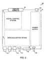
- Fig. 3shows a second embodiment of a circuit board arrangement 20.
- the circuit board arrangement 20includes the single circuit board 3, the data acquisition device 4 and the power supply 5 thereon. As described above, the data acquisition device 4 and the power supply 5 are disposed on the single circuit board 3.
- the single circuit board arrangement 20is positioned in a casing of a digital computer (not shown).
- the single circuit board 3includes a computer connector 22 operably coupling the single circuit board 3 and circuit elements disposed thereon to the digital computer.
- the computer connector 22interfaces with the digital computer via a standard data bus slot (e.g. EISA, ISA, PCI, VXI, etc.) that is connected to the motherboard of the digital computer.
- a standard data bus slote.g. EISA, ISA, PCI, VXI, etc.
- the data acquisition device 4 and the power supply 5may be disposed directly on (or attached directly to) the single circuit board 3 or upon a predetermined number of the daughter boards (e.g., preferably not exceeding three daughter boards) mounted on the single circuit board 3. If the daughter boards are used, these daughter boards should preferably not exceed an area of, e.g., approximately six square inches.
- the single circuit board arrangement 20 according to the second embodimentincludes similar externally accessible input ports, output ports, control systems, and connection systems as described for the first embodiment above.
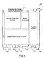
- Figs. 4 and 5show a third embodiment of a circuit board arrangement 23 with the data acquisition device 4 and the power supply 5 arranged on the single circuit board 3.
- the third embodiment of a circuit board arrangement 23includes the similar elements as described above with respect to the first embodiment shown in Fig. 1 and further disposes a signal generator 24 on the single circuit board 3 or on the daughter boards that may be situated on the single circuit board 3, and may communicate with the digital control system 8, the power supply 5 and/or the data acquisition device 4, either directly or indirectly.
- the data/power supply output 15is also included, however, a signal generated output (generated by the signal generator 24) can also be provided using this output port.
- the signal generator 24can be used for providing test signals (either analog or digital) to a user-built (or prefabricated) test circuit, that may be powered by, e.g., the power supply 5, in order to stimulate such test circuit to provide a test output signal. This test output signal can then be measured by, e.g., the data acquisition device 4.
- the signal generator 24can include, e.g., a conventional signal generator as are known in the art.
- the circuit board arrangement 23also includes an externally accessible signal output port 26, which is connected to the signal generator 24, either directly or via the digital control system 8.
- Fig. 6shows a fourth embodiment of a single circuit board arrangement 28 which includes a single circuit board 3, the data acquisition device 4 and the power supply 5.
- the data acquisition device 4 and the power supply 5are disposed on the single circuit board 3.
- the circuit board arrangement 28includes the elements described above in the second embodiment as shown in Fig. 3 and further provides a signal generator 24 on the single circuit board 3 or on the daughter boards that can be situated on the single circuit board 3.
- the circuit board arrangement 28further includes the same externally accessible signal output port 26 as described for the third embodiment above and shown in Figs. 4 and 5.
- the data acquisition device 4can be configured by manually adjusting the externally accessible trigger level control system 14 which can be electrically coupled directly to the data acquisition device 4 or via the digital control system 8.
- the power supply 5can be configured by manually adjusting the externally accessible power supply controller 18 which can be electrically coupled directly to the power supply 5 or also via the digital control system 8.
- the signal generator 24can be configured by manually adjusting the externally accessible signal output port 26 which can be electrically coupled directly to the signal generator 24 or via the digital control system 8.
- the data acquisition device 4, the power supply 5 and/or the signal generator 24can also be adjusted automatically by using, e.g., the digital computer.
- the data acquisition device 4can be configured by a software program operating in the digital computer or by adjusting the externally accessible trigger level control system 14 to function as, e.g., a dual channel storage oscilloscope, a frequency meter, a digital multimeter, or a spectrum analyzer.
- the power supply 5can also be configured by the software program operating in the digital computer and/or by adjusting the externally accessible power supply controller 18 to control the voltage and/or current output.
- the power supply 5is capable of generating either a digital voltage and/or current signal or an analog voltage and/or current signal.
- the type of the signal (i.e., digital or analog) generated by the signal generatorcan be configured by the software program or manually configured.
- the data acquisition device 4, the power supply 5 and/or the signal generator 24can also be controlled using, e.g., the digital control system 8.
Landscapes
- Engineering & Computer Science (AREA)
- General Engineering & Computer Science (AREA)
- Physics & Mathematics (AREA)
- General Physics & Mathematics (AREA)
- Computer Hardware Design (AREA)
- Microelectronics & Electronic Packaging (AREA)
- Tests Of Electronic Circuits (AREA)
- Oscillators With Electromechanical Resonators (AREA)
- Diaphragms For Electromechanical Transducers (AREA)
- Production Of Multi-Layered Print Wiring Board (AREA)
Abstract
Description
Claims (11)
- An electronic circuit board arrangment (1) for testing a test circuitcomprising:a multi-channel data acquisition means (4) foracquiring analog and digital test signals and storing thesignals for processing by a computer (7);a user variable power supply (5) for providing power toan external test circuit for operating the test circuit; anda single circuit board (3) supporting the dataacquisition means (4) and the power supply (5).
- The electronic circuit board arrangement of claim 1,further comprising a user variable signal generator (24),the signal generator providing analog and digital signalsfor general use and disposed on the single circuit board(3).
- The electronic circuit board arrangement of claim 1,further comprising a user variable signal generator (24),the signal generator (24) providing analog and digitalsignals for general use, the single circuit board (3)supporting the user variable signal generator (24), andwherein the multi-channel data acquisition means (4) isfurther provided for communicating through a port of acomputer and providing a storage oscilloscope.
- The electronic circuit board arrangement of claim 1, claim 2 or claim 3,further comprising a digital control system (8) disposed onthe single circuit board (3) and a power supply controller(18), wherein the power supply controller (18) is coupled tothe power supply (5) directly or by the digital controlsystem (8).
- The electronic circuit board arrangement of claim 4when dependent on claim 2, wherein the data acquisitionmeans (4) acquires signals from the test circuit, the powersupply (5) provides multiple power outputs to the testcircuit, the signal generator (24) provides analog anddigital test signals to the test circuit, and acommunications port (6) connected to the data acquisitionmeans (4) or the digital control system (8) provides theacquired signals from the test circuit to a digital computer(7).
- The electronic circuit board arrangement of claim 1 or claim 3, furthercomprising a dedicated housing (2) for the single circuitboard (3).
- The electronic circuit board arrangement of claim 3, further comprisingan externally accessible trigger input (13) for the storageoscilloscope mode of operation.
- The electronic circuit board arrangement of claim 1coupled with a computer (7), and further comprising:wherein the multi-channel data acquisition means (4) isfurther provided for communicating through a port of thecomputer (7) and providing a function.a user variable signal generator (24), the signalgenerator (24) providing analog and digital signals forgeneral use, the single circuit board (3) supporting theuser variable signal generator (24); andsoftware operating in the computer (17) forconfiguring the data acquisition means (4), the power supply(5), and the signal generator (24);
- The electronic circuit board arrangement of claim 1further comprising:wherein the multi-channel data acquisition means (4) isfurther provided for communicating through a port of thecomputer (7) and providing a function.a user variable signal generator (24), the signalgenerator (24) providing analog and digital signals forgeneral use, the single circuit board (3) supporting theuser variable signal generator (24) and contained in adedicated housing (2); andmeans (12, 13, 14, 18) for adjusting the dataacquisition means (4), the power supply (5), or the signalgenerator (24);
- The electronic circuit board arrangement of claim 8 orclaim 9, wherein the function is selected from the groupconsisting of a storage oscilloscope, a frequency meter, adigital multimeter, and a spectrum analyzer.
- The electronic circuit board arrangement of claim 1,claim 3 or claim 9, wherein the single circuit board (3)includes at least one daughter board mounted to the singlecircuit board (3).
Applications Claiming Priority (3)
| Application Number | Priority Date | Filing Date | Title |
|---|---|---|---|
| US914413 | 1997-08-19 | ||
| US08/914,413US6094624A (en) | 1997-08-19 | 1997-08-19 | Electronic test facility |
| PCT/US1998/017020WO1999009623A1 (en) | 1997-08-19 | 1998-08-17 | Circuit board arrangement |
Publications (3)
| Publication Number | Publication Date |
|---|---|
| EP1005708A1 EP1005708A1 (en) | 2000-06-07 |
| EP1005708A4 EP1005708A4 (en) | 2000-11-08 |
| EP1005708B1true EP1005708B1 (en) | 2005-10-26 |
Family
ID=25434329
Family Applications (1)
| Application Number | Title | Priority Date | Filing Date |
|---|---|---|---|
| EP98939969AExpired - LifetimeEP1005708B1 (en) | 1997-08-19 | 1998-08-17 | Circuit board arrangement |
Country Status (9)
| Country | Link |
|---|---|
| US (1) | US6094624A (en) |
| EP (1) | EP1005708B1 (en) |
| JP (1) | JP2001516037A (en) |
| CN (1) | CN1161692C (en) |
| AT (1) | ATE308136T1 (en) |
| AU (1) | AU734069B2 (en) |
| CA (1) | CA2300162A1 (en) |
| DE (1) | DE69832077T2 (en) |
| WO (1) | WO1999009623A1 (en) |
Families Citing this family (12)
| Publication number | Priority date | Publication date | Assignee | Title |
|---|---|---|---|---|
| US6745146B1 (en)* | 1998-10-30 | 2004-06-01 | Avaya Technology Corp. | Automated test system and method for device having circuit and ground connections |
| US6385739B1 (en)* | 1999-07-19 | 2002-05-07 | Tivo Inc. | Self-test electronic assembly and test system |
| WO2003010612A2 (en)* | 2001-07-24 | 2003-02-06 | University Of Delhi | Multifunction interface device for use, inter alia, in laboratory procedures |
| CN1327350C (en)* | 2003-10-30 | 2007-07-18 | 英业达股份有限公司 | Digital signal acquisition system and method |
| CN100517257C (en)* | 2005-10-28 | 2009-07-22 | 鸿富锦精密工业(深圳)有限公司 | High-speed peripheral component interconnection bus interface test device |
| CN101686414B (en)* | 2008-09-26 | 2013-06-05 | 深圳富泰宏精密工业有限公司 | Testing device for mobile phone |
| US8161335B2 (en)* | 2009-05-05 | 2012-04-17 | Bae Systems Information And Electronic Systems Integration Inc. | System and method for testing a circuit |
| CN102645627B (en)* | 2012-03-09 | 2014-06-25 | 中国南方电网有限责任公司超高压输电公司检修试验中心 | Closed-loop test system for IO (input/output) channel signals of analog board in RTDS (real time digital simulator) |
| EP3382408B1 (en) | 2017-03-30 | 2025-05-28 | Rohde & Schwarz GmbH & Co. KG | Measurement device and method for measuring a device under test |
| US10620091B2 (en) | 2017-11-17 | 2020-04-14 | Hamilton Sundstrand Corporation | Electronic control system tester |
| US11307061B2 (en)* | 2018-03-08 | 2022-04-19 | Rohde & Schwarz Gmbh & Co. Kg | Electrical measurement device |
| CN111077431A (en)* | 2019-12-30 | 2020-04-28 | 浙江力创自动化科技有限公司 | A kind of electrical performance testing equipment for control circuit board |
Citations (3)
| Publication number | Priority date | Publication date | Assignee | Title |
|---|---|---|---|---|
| US4380764A (en)* | 1981-03-12 | 1983-04-19 | Data Translation, Inc. | Data acquisition apparatus |
| EP0347632A1 (en)* | 1988-06-20 | 1989-12-27 | Regeltron Computer Gmbh | Apparatus for automatically detecting and recording measured values |
| DE19603942A1 (en)* | 1996-02-05 | 1997-08-07 | Eps Electronic Production Schl | Data acquisition device for automatic independent acquisition and storage of electrical parameters |
Family Cites Families (21)
| Publication number | Priority date | Publication date | Assignee | Title |
|---|---|---|---|---|
| US4238784A (en)* | 1975-01-23 | 1980-12-09 | Colt Industries Operating Corp. | Electronic measuring system with pulsed power supply and stability sensing |
| US4072851A (en)* | 1976-03-26 | 1978-02-07 | Norland Corporation | Waveform measuring instrument with resident programmed processor for controlled waveform display and waveform data reduction and calculation |
| US4571689A (en)* | 1982-10-20 | 1986-02-18 | The United States Of America As Represented By The Secretary Of The Air Force | Multiple thermocouple testing device |
| US4747060A (en)* | 1986-03-31 | 1988-05-24 | Halliburton Company | Data acquisition module and method |
| US4758779A (en)* | 1986-04-07 | 1988-07-19 | Tektronix, Inc. | Probe body for an electrical measurement system |
| US4862067A (en)* | 1987-06-24 | 1989-08-29 | Schlumberger Technologies, Inc. | Method and apparatus for in-circuit testing of electronic devices |
| JPH01180645A (en)* | 1988-01-13 | 1989-07-18 | Hitachi Ltd | Automatic verification method of maintenance diagnosis mechanism |
| US5014226A (en)* | 1988-09-29 | 1991-05-07 | Lsi Logic Corporation | Method and apparatus for predicting the metastable behavior of logic circuits |
| US5307290A (en)* | 1988-10-18 | 1994-04-26 | Fiat Auto S.P.A. | System for the automatic testing, preferably on a bench, of electronic control systems which are intended to be fitted in vehicles |
| US5003486A (en)* | 1989-02-24 | 1991-03-26 | Nero Technologies Ltd. | Programmable safety electrical socket controller |
| IE80813B1 (en)* | 1989-05-16 | 1999-03-10 | Formia Limited | Electronic test systems |
| US5058112A (en)* | 1989-07-31 | 1991-10-15 | Ag Communication Systems Corporation | Programmable fault insertion circuit |
| US5345392A (en)* | 1991-01-25 | 1994-09-06 | International Business Machines Corporation | Battery charge monitor for a personal computer |
| US5254992A (en)* | 1991-10-31 | 1993-10-19 | Fairbanks Inc. | Low power electronic measuring system |
| US5396168A (en)* | 1992-03-27 | 1995-03-07 | Tandy Corporation | Digital multimeter with microprocessor control |
| US5406495A (en)* | 1993-02-01 | 1995-04-11 | Systems Analysis And Integration, Inc. | Substation load distribution monitor system |
| US5459671A (en)* | 1993-02-19 | 1995-10-17 | Advanced Micro Devices, Inc. | Programmable battery controller |
| US5526287A (en)* | 1994-07-01 | 1996-06-11 | Ada Technologies, Inc. | Portable data collection device |
| US5544107A (en)* | 1994-08-22 | 1996-08-06 | Adaptec, Inc. | Diagnostic data port for a LSI or VLSI integrated circuit |
| US5852737A (en)* | 1995-04-24 | 1998-12-22 | National Semiconductor Corporation | Method and apparatus for operating digital static CMOS components in a very low voltage mode during power-down |
| US5790839A (en)* | 1996-12-20 | 1998-08-04 | International Business Machines Corporation | System integration of DRAM macros and logic cores in a single chip architecture |
- 1997
- 1997-08-19USUS08/914,413patent/US6094624A/ennot_activeExpired - Lifetime
- 1998
- 1998-08-17CACA002300162Apatent/CA2300162A1/ennot_activeAbandoned
- 1998-08-17AUAU88307/98Apatent/AU734069B2/ennot_activeCeased
- 1998-08-17WOPCT/US1998/017020patent/WO1999009623A1/enactiveIP Right Grant
- 1998-08-17CNCNB988103168Apatent/CN1161692C/ennot_activeExpired - Fee Related
- 1998-08-17JPJP2000510187Apatent/JP2001516037A/enactivePending
- 1998-08-17ATAT98939969Tpatent/ATE308136T1/ennot_activeIP Right Cessation
- 1998-08-17DEDE69832077Tpatent/DE69832077T2/ennot_activeExpired - Fee Related
- 1998-08-17EPEP98939969Apatent/EP1005708B1/ennot_activeExpired - Lifetime
Patent Citations (3)
| Publication number | Priority date | Publication date | Assignee | Title |
|---|---|---|---|---|
| US4380764A (en)* | 1981-03-12 | 1983-04-19 | Data Translation, Inc. | Data acquisition apparatus |
| EP0347632A1 (en)* | 1988-06-20 | 1989-12-27 | Regeltron Computer Gmbh | Apparatus for automatically detecting and recording measured values |
| DE19603942A1 (en)* | 1996-02-05 | 1997-08-07 | Eps Electronic Production Schl | Data acquisition device for automatic independent acquisition and storage of electrical parameters |
Also Published As
| Publication number | Publication date |
|---|---|
| US6094624A (en) | 2000-07-25 |
| AU8830798A (en) | 1999-03-08 |
| EP1005708A1 (en) | 2000-06-07 |
| EP1005708A4 (en) | 2000-11-08 |
| DE69832077T2 (en) | 2006-07-13 |
| CA2300162A1 (en) | 1999-02-25 |
| AU734069B2 (en) | 2001-05-31 |
| WO1999009623A1 (en) | 1999-02-25 |
| CN1161692C (en) | 2004-08-11 |
| CN1276925A (en) | 2000-12-13 |
| DE69832077D1 (en) | 2005-12-01 |
| JP2001516037A (en) | 2001-09-25 |
| ATE308136T1 (en) | 2005-11-15 |
Similar Documents
| Publication | Publication Date | Title |
|---|---|---|
| CN1987487B (en) | Accessory device voltage management system controlled by a host | |
| EP1005708B1 (en) | Circuit board arrangement | |
| US5479610A (en) | System interface fault isolator test set | |
| JP4869545B2 (en) | Voltage management device for measuring equipment | |
| WO2005022172A1 (en) | A digital multi-meter | |
| CN104133139A (en) | Multifunctional PXI module integration testing instrument and testing method thereof | |
| US5939875A (en) | Universal probe interface | |
| TW200416547A (en) | Probe based information storage for probes used for opens detection in in-circuit testing | |
| GB2194348A (en) | Multimeters | |
| KR100723611B1 (en) | Voltage management system for measurement test equipment using accessories | |
| CN107179451A (en) | Integrated low frequency noise measurement device | |
| US5804971A (en) | Modular card based meter | |
| US6564158B1 (en) | Broadband electromagnetic field component measurement system | |
| US5359327A (en) | A/D converter system with interface and passive voltage reference source | |
| CN206990690U (en) | Low frequency noise measurement device | |
| EP0157028A1 (en) | Programmable tester | |
| CN107015556A (en) | A kind of bus solid-state power controller test device | |
| US6513086B1 (en) | Signal conditioning system including low voltage and high voltage analog buses | |
| CN215448014U (en) | Main structure, checking device, pressure, process and temperature and humidity checking or recording instrument | |
| CN108008345A (en) | Buckle type single-phase electric energy meter on-site calibration instrument | |
| CN112486237B (en) | Multi-channel high-precision micro-current source for nuclear power reactor core nuclear measurement system | |
| CN106771613B (en) | A kind of cable crimping resistance nondestructive measurement system | |
| CN212514752U (en) | Voltage detector | |
| CN120761945A (en) | Integrated calibration system for insulation resistance meter and withstand voltage tester | |
| Harris et al. | 16-channel PC-based aircraft electrical power monitor |
Legal Events
| Date | Code | Title | Description |
|---|---|---|---|
| PUAI | Public reference made under article 153(3) epc to a published international application that has entered the european phase | Free format text:ORIGINAL CODE: 0009012 | |
| 17P | Request for examination filed | Effective date:20000308 | |
| AK | Designated contracting states | Kind code of ref document:A1 Designated state(s):AT BE CH CY DE DK ES FI FR GB GR IE IT LI LU MC NL PT SE | |
| A4 | Supplementary search report drawn up and despatched | Effective date:20000927 | |
| AK | Designated contracting states | Kind code of ref document:A4 Designated state(s):AT BE CH CY DE DK ES FI FR GB GR IE IT LI LU MC NL PT SE | |
| RIC1 | Information provided on ipc code assigned before grant | Free format text:7H 01S 3/10 A, 7G 06F 11/267 B | |
| 17Q | First examination report despatched | Effective date:20040401 | |
| GRAP | Despatch of communication of intention to grant a patent | Free format text:ORIGINAL CODE: EPIDOSNIGR1 | |
| GRAS | Grant fee paid | Free format text:ORIGINAL CODE: EPIDOSNIGR3 | |
| GRAA | (expected) grant | Free format text:ORIGINAL CODE: 0009210 | |
| AK | Designated contracting states | Kind code of ref document:B1 Designated state(s):AT BE CH CY DE DK ES FI FR GB GR IE IT LI LU MC NL PT SE | |
| PG25 | Lapsed in a contracting state [announced via postgrant information from national office to epo] | Ref country code:NL Free format text:LAPSE BECAUSE OF FAILURE TO SUBMIT A TRANSLATION OF THE DESCRIPTION OR TO PAY THE FEE WITHIN THE PRESCRIBED TIME-LIMIT Effective date:20051026 Ref country code:LI Free format text:LAPSE BECAUSE OF FAILURE TO SUBMIT A TRANSLATION OF THE DESCRIPTION OR TO PAY THE FEE WITHIN THE PRESCRIBED TIME-LIMIT Effective date:20051026 Ref country code:IT Free format text:LAPSE BECAUSE OF FAILURE TO SUBMIT A TRANSLATION OF THE DESCRIPTION OR TO PAY THE FEE WITHIN THE PRESCRIBED TIME-LIMIT;WARNING: LAPSES OF ITALIAN PATENTS WITH EFFECTIVE DATE BEFORE 2007 MAY HAVE OCCURRED AT ANY TIME BEFORE 2007. THE CORRECT EFFECTIVE DATE MAY BE DIFFERENT FROM THE ONE RECORDED. Effective date:20051026 Ref country code:FI Free format text:LAPSE BECAUSE OF FAILURE TO SUBMIT A TRANSLATION OF THE DESCRIPTION OR TO PAY THE FEE WITHIN THE PRESCRIBED TIME-LIMIT Effective date:20051026 Ref country code:CH Free format text:LAPSE BECAUSE OF FAILURE TO SUBMIT A TRANSLATION OF THE DESCRIPTION OR TO PAY THE FEE WITHIN THE PRESCRIBED TIME-LIMIT Effective date:20051026 Ref country code:BE Free format text:LAPSE BECAUSE OF FAILURE TO SUBMIT A TRANSLATION OF THE DESCRIPTION OR TO PAY THE FEE WITHIN THE PRESCRIBED TIME-LIMIT Effective date:20051026 Ref country code:AT Free format text:LAPSE BECAUSE OF FAILURE TO SUBMIT A TRANSLATION OF THE DESCRIPTION OR TO PAY THE FEE WITHIN THE PRESCRIBED TIME-LIMIT Effective date:20051026 | |
| REG | Reference to a national code | Ref country code:GB Ref legal event code:FG4D | |
| REG | Reference to a national code | Ref country code:CH Ref legal event code:EP | |
| REG | Reference to a national code | Ref country code:IE Ref legal event code:FG4D | |
| REF | Corresponds to: | Ref document number:69832077 Country of ref document:DE Date of ref document:20051201 Kind code of ref document:P | |
| PG25 | Lapsed in a contracting state [announced via postgrant information from national office to epo] | Ref country code:SE Free format text:LAPSE BECAUSE OF FAILURE TO SUBMIT A TRANSLATION OF THE DESCRIPTION OR TO PAY THE FEE WITHIN THE PRESCRIBED TIME-LIMIT Effective date:20060126 Ref country code:GR Free format text:LAPSE BECAUSE OF FAILURE TO SUBMIT A TRANSLATION OF THE DESCRIPTION OR TO PAY THE FEE WITHIN THE PRESCRIBED TIME-LIMIT Effective date:20060126 Ref country code:DK Free format text:LAPSE BECAUSE OF FAILURE TO SUBMIT A TRANSLATION OF THE DESCRIPTION OR TO PAY THE FEE WITHIN THE PRESCRIBED TIME-LIMIT Effective date:20060126 | |
| PG25 | Lapsed in a contracting state [announced via postgrant information from national office to epo] | Ref country code:ES Free format text:LAPSE BECAUSE OF FAILURE TO SUBMIT A TRANSLATION OF THE DESCRIPTION OR TO PAY THE FEE WITHIN THE PRESCRIBED TIME-LIMIT Effective date:20060206 | |
| PG25 | Lapsed in a contracting state [announced via postgrant information from national office to epo] | Ref country code:PT Free format text:LAPSE BECAUSE OF FAILURE TO SUBMIT A TRANSLATION OF THE DESCRIPTION OR TO PAY THE FEE WITHIN THE PRESCRIBED TIME-LIMIT Effective date:20060327 | |
| NLV1 | Nl: lapsed or annulled due to failure to fulfill the requirements of art. 29p and 29m of the patents act | ||
| REG | Reference to a national code | Ref country code:CH Ref legal event code:PL | |
| ET | Fr: translation filed | ||
| PGFP | Annual fee paid to national office [announced via postgrant information from national office to epo] | Ref country code:FR Payment date:20060808 Year of fee payment:9 | |
| PGFP | Annual fee paid to national office [announced via postgrant information from national office to epo] | Ref country code:DE Payment date:20060810 Year of fee payment:9 | |
| PGFP | Annual fee paid to national office [announced via postgrant information from national office to epo] | Ref country code:GB Payment date:20060816 Year of fee payment:9 | |
| PG25 | Lapsed in a contracting state [announced via postgrant information from national office to epo] | Ref country code:IE Free format text:LAPSE BECAUSE OF NON-PAYMENT OF DUE FEES Effective date:20060817 | |
| PG25 | Lapsed in a contracting state [announced via postgrant information from national office to epo] | Ref country code:MC Free format text:LAPSE BECAUSE OF NON-PAYMENT OF DUE FEES Effective date:20060831 | |
| PLBE | No opposition filed within time limit | Free format text:ORIGINAL CODE: 0009261 | |
| STAA | Information on the status of an ep patent application or granted ep patent | Free format text:STATUS: NO OPPOSITION FILED WITHIN TIME LIMIT | |
| 26N | No opposition filed | Effective date:20060727 | |
| REG | Reference to a national code | Ref country code:IE Ref legal event code:MM4A | |
| GBPC | Gb: european patent ceased through non-payment of renewal fee | Effective date:20070817 | |
| REG | Reference to a national code | Ref country code:FR Ref legal event code:ST Effective date:20080430 | |
| PG25 | Lapsed in a contracting state [announced via postgrant information from national office to epo] | Ref country code:LU Free format text:LAPSE BECAUSE OF NON-PAYMENT OF DUE FEES Effective date:20060817 Ref country code:DE Free format text:LAPSE BECAUSE OF NON-PAYMENT OF DUE FEES Effective date:20080301 | |
| PG25 | Lapsed in a contracting state [announced via postgrant information from national office to epo] | Ref country code:FR Free format text:LAPSE BECAUSE OF NON-PAYMENT OF DUE FEES Effective date:20070831 | |
| PG25 | Lapsed in a contracting state [announced via postgrant information from national office to epo] | Ref country code:GB Free format text:LAPSE BECAUSE OF NON-PAYMENT OF DUE FEES Effective date:20070817 Ref country code:CY Free format text:LAPSE BECAUSE OF FAILURE TO SUBMIT A TRANSLATION OF THE DESCRIPTION OR TO PAY THE FEE WITHIN THE PRESCRIBED TIME-LIMIT Effective date:20051026 |