EP1003219B1 - DRAM with stacked capacitor and buried word line - Google Patents
DRAM with stacked capacitor and buried word lineDownload PDFInfo
- Publication number
- EP1003219B1 EP1003219B1EP99119420AEP99119420AEP1003219B1EP 1003219 B1EP1003219 B1EP 1003219B1EP 99119420 AEP99119420 AEP 99119420AEP 99119420 AEP99119420 AEP 99119420AEP 1003219 B1EP1003219 B1EP 1003219B1
- Authority
- EP
- European Patent Office
- Prior art keywords
- layer
- trench
- semiconductor body
- dielectric
- over
- Prior art date
- Legal status (The legal status is an assumption and is not a legal conclusion. Google has not performed a legal analysis and makes no representation as to the accuracy of the status listed.)
- Expired - Lifetime
Links
- 239000003990capacitorSubstances0.000titleclaimsdescription32
- 230000015654memoryEffects0.000claimsdescription30
- 239000004065semiconductorSubstances0.000claimsdescription30
- 238000003860storageMethods0.000claimsdescription21
- XUIMIQQOPSSXEZ-UHFFFAOYSA-NSiliconChemical compound[Si]XUIMIQQOPSSXEZ-UHFFFAOYSA-N0.000claimsdescription15
- 229910052710siliconInorganic materials0.000claimsdescription15
- 239000010703siliconSubstances0.000claimsdescription15
- 229910021420polycrystalline siliconInorganic materials0.000claimsdescription12
- 229920005591polysiliconPolymers0.000claimsdescription12
- 238000000034methodMethods0.000claimsdescription10
- FVBUAEGBCNSCDD-UHFFFAOYSA-Nsilicide(4-)Chemical group[Si-4]FVBUAEGBCNSCDD-UHFFFAOYSA-N0.000claimsdescription9
- 229910021332silicideInorganic materials0.000claimsdescription8
- VYPSYNLAJGMNEJ-UHFFFAOYSA-NSilicium dioxideChemical compoundO=[Si]=OVYPSYNLAJGMNEJ-UHFFFAOYSA-N0.000claimsdescription7
- 239000004020conductorSubstances0.000claimsdescription7
- 229910052814silicon oxideInorganic materials0.000claimsdescription7
- 239000000463materialSubstances0.000claimsdescription5
- 229910021421monocrystalline siliconInorganic materials0.000claimsdescription4
- 238000011049fillingMethods0.000claimsdescription3
- 238000002955isolationMethods0.000claimsdescription3
- 239000003989dielectric materialSubstances0.000claimsdescription2
- 239000010410layerSubstances0.000description31
- 125000006850spacer groupChemical group0.000description10
- 239000000758substrateSubstances0.000description8
- 238000001020plasma etchingMethods0.000description5
- 229910052581Si3N4Inorganic materials0.000description3
- BOTDANWDWHJENH-UHFFFAOYSA-NTetraethyl orthosilicateChemical compoundCCO[Si](OCC)(OCC)OCCBOTDANWDWHJENH-UHFFFAOYSA-N0.000description3
- 229910052751metalInorganic materials0.000description3
- 239000002184metalSubstances0.000description3
- 230000002093peripheral effectEffects0.000description3
- HQVNEWCFYHHQES-UHFFFAOYSA-Nsilicon nitrideChemical compoundN12[Si]34N5[Si]62N3[Si]51N64HQVNEWCFYHHQES-UHFFFAOYSA-N0.000description3
- 229910052454barium strontium titanateInorganic materials0.000description2
- 230000015572biosynthetic processEffects0.000description2
- 238000005229chemical vapour depositionMethods0.000description2
- -1chipSubstances0.000description2
- 238000005530etchingMethods0.000description2
- 230000005669field effectEffects0.000description2
- 238000005468ion implantationMethods0.000description2
- BASFCYQUMIYNBI-UHFFFAOYSA-NplatinumChemical compound[Pt]BASFCYQUMIYNBI-UHFFFAOYSA-N0.000description2
- 238000000576coating methodMethods0.000description1
- 230000000295complement effectEffects0.000description1
- 238000000151depositionMethods0.000description1
- 230000008021depositionEffects0.000description1
- 239000012212insulatorSubstances0.000description1
- 238000010884ion-beam techniqueMethods0.000description1
- 230000000873masking effectEffects0.000description1
- 229910044991metal oxideInorganic materials0.000description1
- 150000004706metal oxidesChemical class0.000description1
- 238000000059patterningMethods0.000description1
- 229910052697platinumInorganic materials0.000description1
- 238000005498polishingMethods0.000description1
- 238000002360preparation methodMethods0.000description1
- VBIZUNYMJSPHBH-OQLLNIDSSA-NsalinazidChemical compoundOC1=CC=CC=C1\C=N\NC(=O)C1=CC=NC=C1VBIZUNYMJSPHBH-OQLLNIDSSA-N0.000description1
- 229950007671salinazidDrugs0.000description1
- 238000000926separation methodMethods0.000description1
- 239000005368silicate glassSubstances0.000description1
- 239000002356single layerSubstances0.000description1
- 239000000126substanceSubstances0.000description1
- 229910052721tungstenInorganic materials0.000description1
- WQJQOUPTWCFRMM-UHFFFAOYSA-Ntungsten disilicideChemical compound[Si]#[W]#[Si]WQJQOUPTWCFRMM-UHFFFAOYSA-N0.000description1
- 229910021342tungsten silicideInorganic materials0.000description1
Images


Classifications
- H—ELECTRICITY
- H10—SEMICONDUCTOR DEVICES; ELECTRIC SOLID-STATE DEVICES NOT OTHERWISE PROVIDED FOR
- H10B—ELECTRONIC MEMORY DEVICES
- H10B12/00—Dynamic random access memory [DRAM] devices
- H10B12/30—DRAM devices comprising one-transistor - one-capacitor [1T-1C] memory cells
- H10B12/31—DRAM devices comprising one-transistor - one-capacitor [1T-1C] memory cells having a storage electrode stacked over the transistor
- H—ELECTRICITY
- H10—SEMICONDUCTOR DEVICES; ELECTRIC SOLID-STATE DEVICES NOT OTHERWISE PROVIDED FOR
- H10B—ELECTRONIC MEMORY DEVICES
- H10B12/00—Dynamic random access memory [DRAM] devices
- H—ELECTRICITY
- H10—SEMICONDUCTOR DEVICES; ELECTRIC SOLID-STATE DEVICES NOT OTHERWISE PROVIDED FOR
- H10B—ELECTRONIC MEMORY DEVICES
- H10B12/00—Dynamic random access memory [DRAM] devices
- H10B12/01—Manufacture or treatment
- H10B12/02—Manufacture or treatment for one transistor one-capacitor [1T-1C] memory cells
- H10B12/05—Making the transistor
- H10B12/053—Making the transistor the transistor being at least partially in a trench in the substrate
- H—ELECTRICITY
- H10—SEMICONDUCTOR DEVICES; ELECTRIC SOLID-STATE DEVICES NOT OTHERWISE PROVIDED FOR
- H10B—ELECTRONIC MEMORY DEVICES
- H10B12/00—Dynamic random access memory [DRAM] devices
- H10B12/30—DRAM devices comprising one-transistor - one-capacitor [1T-1C] memory cells
- H10B12/34—DRAM devices comprising one-transistor - one-capacitor [1T-1C] memory cells the transistor being at least partially in a trench in the substrate
Definitions
- This inventionrelates to a dynamic random access memory (DRAM) that uses as the memory cell a series combination of a transistor and a storage capacitor, and more particularly, to a DRAM of the kind in which the storage capacitor is formed as a multilayer stack on the top surface of a semiconductor body (substrate, chip) in which has been formed the transistor.
- DRAMdynamic random access memory
- DRAMs of the kind described abovehave become one of the more important of the integrated circuit devices. Moreover, the trend is to memories of larger and larger capacities. To increase the capacity of a memory, it is important to increase the density and decrease the size of the memory cells that are used to form the memory.
- the memory cells of the memoryare arranged in rows and columns in a semiconductor body (silicon chip, substrate) and binary digits (bits) are read-in and read-out of the individual cells by means of bit lines and word lines that typically are provided by conductive layers that run over the surface of the chip spaced apart by dielectric layers.
- the transistorsare formed in a silicon integrated circuit chip and the storage capacitors are formed as multilayer stacks over a top surface of the chip.
- the density of memory cellshas increased, it has become more difficult to locate such stacked capacitors on the surface while maintaining the necessary electric isolation between individual capacitors and between the capacitors and the bit and word lines, all of which are competing for space on the surface of the chip.
- US 5,502,320discloses a stacked capacitor memory device having a buried word line in a trench arranged between regions serving as source and drain of a memory MOSFET.
- US 5,307,310discloses a memory cell having a silicided word line.
- the present inventionseeks to reduce the competition for space between individual capacitors, and between the capacitors and the bit and word lines by burying the word lines that are normally above the surface of a semiconductor body (substrate, chip) into the interior of the semiconductor body.
- the word linesare buried below the storage capacitors and the bit lines. The space freed by so locating the word lines can be used to increase the separation that can be provided to the storage capacitors and the bit lines that still remain in the space above the semiconductor body surface.
- MOSFETmetal-oxide semiconductor field effect
- IGFETinsulated gate field effect transistor
- semiconductor body 10is monocrystalline of p-type conductivity and can be a layer either as a well in a substrate of either p-type and n-type conductivity.
- the p-type layercan be formed as an epitaxial layer grown on a suitable substrate, either of silicon or an insulator.
- PAD layer 11Athat typically includes an underlying layer of silicon oxide and an overlying layer of silicon nitride.
- the PAD layer 11Ais shown as a single layer in the interest of simplicity.
- This PAD layerhas been patterned to expose regions where there will be formed shallow trenches filled with a dielectric material, typically silicon oxide, that will serve to isolate the memory cells from one another.
- Oxide filled trenches 12are shown at the two ends of the body 10.
- the shallow oxide filled trenchestypically are about 2500 Angstroms deep and surround the active areas, typically of square or rectangular shape, in which are largely formed individual pairs of memory cells.
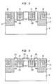
- FIG. 2shows the semiconductor body 10 has been etched to form vertical trenches 13 therein in a central region thereof and in the oxide-filled trenches 12. Typically this can be done by first removing the remainder of the original PAD layer 11A, forming a second PAD layer 11B over the surface, patterning it to form a mask that is used in a reactive ion etching (RIE) to define the vertical trenches 13 shown.
- RIEreactive ion etching
- the trenches 13typically can be about 2000 Angstroms deep and those in the semiconductor body 10 eventually house buried word lines.
- the walls of the trenches 13also will define the channels and the gate electrodes.
- a dielectric layersuitable for use as the gate dielectric, and including two vertical segments 14A and 14C, and a horizontal segment 14B, is formed over sidewalls and a bottom of each trench 13.
- the walls and bottomcan be subjected to ion implantation to set separately the threshold voltage of each of the three channel portions that will be formed adjacent the three dielectric segments 14A, 14B, and 14C.
- Each of these three segmentsis be subjected to ion implantation from a different one of three different ion beam directions, making it possible to provide, if desired, a different threshold voltage V T for each segment.
- these shallow central trenches 13have now been partially filled with doped polysilicon fill 15 that will serve as the gate conductors.
- the top level of the polysilicon fillis made to be below the level of the top surface 10A of the semiconductor body 10, typically about 500 Angstroms below, to insure that the word line remains buried below the top surface 10A of the semiconductor body 10. This typically can be accomplished by conformal deposition of the polysilicon to overfill the trenches 13 and then using reactive ion etching to form recesses in the fill to below the surface 10A.
- FIG. 4shows suitable spacers 16 formed over the sidewalls of the trenches 13 about 150 Angstroms thick. These can be formed by first filling the trenches 13 and then using reactive ion etching to form a central opening leaving the sidewall spacers 16. With the spacers 16 in place, there can now be formed a recess in each of the polysilicon fill 15 without disturbing the gate oxide layer 14A, 14B and 14C that is in place along the side walls and bottom of the gate conductor polysilicon fill 15 that will provide the word line.
- each recess formed in the polysilicon gate conductors 15is filled with fill 17 of a silicide, such as tungsten silicide, to increase the its conductivity for use as the word line.
- a silicidesuch as tungsten silicide
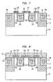
- FIG. 5shows the second PAD layer 11B and the spacers 16 have been stripped away, and the recess left by their removal filled with a dielectric, typically silicon oxide 18. This can be done by chemical vapor deposition (CVD) of silicon oxide to cover the surface and then chemical mechanical polishing (CMP) to planarize the surface using the monocrystalline silicon as an etch stop.
- CVDchemical vapor deposition
- CMPchemical mechanical polishing
- the word lineincluding the doped polysilicon 15 and silicide 17, is completely surrounded by dielectric from gate dielectric 14 or the new dielectric 18 and is located below the surface 10A, a main feature of the process of the present invention.
- the result shown in FIG. 5could have been obtained by stripping only the spacers 16, and removing the PAD layers 11B only after the oxide has been formed to the desired level, leaving the structure shown.
- FIG. 6shows n+ type conductivity regions 20, 21 and 22 have been formed just below the surface 10A of the semiconductor body 10.
- regions 20 and 22will be described separate as sources and region 21 as the common drain for the two transistors being formed in one active area.
- the sources and drains of the transistorexchange roles during the read-in and read-out operations, but it is conventional to describe the region that is connected to the bit line as the drain and the region that is connected to the storage node of the storage capacitor as the source.
- n+ type conductivity epitaxial contact regions 25A, 25B, and 25Cthat have been respectively grown selectively over the monocrystalline silicon source/drain regions 20, 22, and 21, respectively, to provide further elevation and possible lateral expansion of these regions to simplify the provision of source and drain contacts. It can be appreciated that this step is optional.
- the source contacts 25A and 25B and drain contact 25Chave been each surrounded by coatings 27A, 27B, and 27C, respectively, of a silicide, typically Ti or W silicide, to improve their conductivity. Because the elevated source and drain contacts 25A, 25B, and 25C are well defined, the silicide contacts are desirably self aligned (salizide contacts).
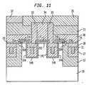
- FIG. 8shows stacked capacitors over the surface 10A of the semiconductor body 10.
- a dielectric layer 29 of a material with a high dielectric constant suitable for use as the dielectric of the storage capacitorfor example barium strontium titanate (BSTO)
- BSTObarium strontium titanate
- the second plateis typically kept at the ground or reference potential so that a single continuous layer of platinum can serve as the second plate of each storage capacitor in the DRAM.
- the lower or first plate of the capacitorsis provided by the individual raised salicidized contacts 25A and 25B, and 27A and 27B that also serve as the source contacts.
- capacitor-source contactshave been formed essentially without the need for any patterned etching.
- a dielectric capsuch as a layer 31 of boro-phosphide silicate glass (BPSG) has been deposited over the top of layer 30.
- BPSGboro-phosphide silicate glass
- a masking layer denoted aboveis first removed and then layer 30 is deposited over the peripheral areas at the same time it is deposited over the memory cell areas. Then a central portion of layers 31, 30, and 29 above semiconductor body 10 is removed by localized etching to leave exposed the salicidized drain contact 27C.
- dielectric spacers 33are provided over the sidewalls of the opening that had been formed in the BPSG. These typically are formed by filling the opening with a suitable spacer dielectric, such as silicon nitride, after which RIE is used to form an opening in the silicon nitride to leave the spacers 33. Now, the opening is overfilled with a suitable bit line contact material, such as doped polysilicon or a metal, after which the surface is planarized by CMP to leave the bit-line contact plug 34 in place.
- a suitable spacer dielectricsuch as silicon nitride
- FIG. 11there is realized the result shown in FIG. 11 in which there has been added the bit line 35 making contact to the bit line contact plug 34.
- the interlevel TEOS dielectric 37can be first deposited and planarized over the top surface of the BPSG. Then the TEOS and the BPSG can be patterned and etched to a level below that of the contact plug 34, after which the wiring metal can be deposited and planarized also to achieve the result shown in FIG. 11 .
- the layer 37 of the interlevel dielectrictypically the silicon oxide described as TEOS that has become popular in the art for this purpose.
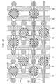
- FIGS. 12 , 13 , and 14are a top view illustrating various possible layouts of the memory cells of a memory array of a DRAM.
- the word lines 40 of which eight are shown in FIGS. 12 and 13 and six are shown in FIG. 14extend vertically and the bit lines 41, of which only two are shown for purposes of simplification, extending horizontally.
- the location of the bit line contactsare shown by the inner circles 43 that are shown surrounded by the outer circles 44, representing spacer layers.
- the location of epitaxial grown silicon regions that serve as the lower plate of the storage capacitorsare represented by the circles 45.
- the shallow oxide-filled isolation trenchesare excluded in areas 46.
- FIGS. 1-11essentially represent cross-sections taken along the dashed line X-X of FIG. 12 .
Landscapes
- Engineering & Computer Science (AREA)
- Manufacturing & Machinery (AREA)
- Semiconductor Memories (AREA)
Description
- This invention relates to a dynamic random access memory (DRAM) that uses as the memory cell a series combination of a transistor and a storage capacitor, and more particularly, to a DRAM of the kind in which the storage capacitor is formed as a multilayer stack on the top surface of a semiconductor body (substrate, chip) in which has been formed the transistor.
- DRAMs of the kind described above have become one of the more important of the integrated circuit devices. Moreover, the trend is to memories of larger and larger capacities. To increase the capacity of a memory, it is important to increase the density and decrease the size of the memory cells that are used to form the memory.
- In the typical DRAM, the memory cells of the memory are arranged in rows and columns in a semiconductor body (silicon chip, substrate) and binary digits (bits) are read-in and read-out of the individual cells by means of bit lines and word lines that typically are provided by conductive layers that run over the surface of the chip spaced apart by dielectric layers.
- In a popular form of DRAM the transistors are formed in a silicon integrated circuit chip and the storage capacitors are formed as multilayer stacks over a top surface of the chip. As the density of memory cells has increased, it has become more difficult to locate such stacked capacitors on the surface while maintaining the necessary electric isolation between individual capacitors and between the capacitors and the bit and word lines, all of which are competing for space on the surface of the chip.
US 5,502,320 discloses a stacked capacitor memory device having a buried word line in a trench arranged between regions serving as source and drain of a memory MOSFET.US 5,307,310 discloses a memory cell having a silicided word line.- The present invention seeks to reduce the competition for space between individual capacitors, and between the capacitors and the bit and word lines by burying the word lines that are normally above the surface of a semiconductor body (substrate, chip) into the interior of the semiconductor body. In particular, the word lines are buried below the storage capacitors and the bit lines. The space freed by so locating the word lines can be used to increase the separation that can be provided to the storage capacitors and the bit lines that still remain in the space above the semiconductor body surface.
- This problem is solved by the memory cell of claim 1 and the method of claim 6.
- The invention will be better understood from the following more detailed description taken in conjunction with the accompanying drawing.
FIGS. 1-11 show cross sections of a semiconductor body (substrate, chip, silicon wafer) at different stages of formation of a pair of memory cells therein in accordance with the present invention; andFIGS. 12 ,13 , and14 show schematic top views of transistors, storage capacitors, word lines, and bit lines of a DRAM in accordance with the present invention.- It will be convenient to describe the invention with reference to a portion of a semiconductor body (chip, substrate), in which the memory is formed that is of a size sufficient to form a pair of memory cells. As is known, typically most of the processing of a DRAM is done on a wafer scale, after which the wafer is diced into individual chips of a single DRAM for the final steps of the processing.
- The process will be described specifically with reference to the preparation of memory cells that use an n-channel metal-oxide semiconductor field effect (MOSFET), also denoted as an insulated gate field effect transistor (IGFET), as the transistor. To this end, there is first prepared a semiconductor body (silicon chip, substrate, workpiece) 10 that includes at least at a
top surface 10A thereof. In an illustrativeembodiment semiconductor body 10 is monocrystalline of p-type conductivity and can be a layer either as a well in a substrate of either p-type and n-type conductivity. Alternatively, the p-type layer can be formed as an epitaxial layer grown on a suitable substrate, either of silicon or an insulator. - It is usual to begin the processing by forming over a
surface 10A of semiconductor body 10 a "PAD"layer 11A that typically includes an underlying layer of silicon oxide and an overlying layer of silicon nitride. ThePAD layer 11A is shown as a single layer in the interest of simplicity. This PAD layer has been patterned to expose regions where there will be formed shallow trenches filled with a dielectric material, typically silicon oxide, that will serve to isolate the memory cells from one another. Oxide filledtrenches 12 are shown at the two ends of thebody 10. The shallow oxide filled trenches typically are about 2500 Angstroms deep and surround the active areas, typically of square or rectangular shape, in which are largely formed individual pairs of memory cells. FIG. 2 shows thesemiconductor body 10 has been etched to formvertical trenches 13 therein in a central region thereof and in the oxide-filledtrenches 12. Typically this can be done by first removing the remainder of theoriginal PAD layer 11A, forming a second PAD layer 11B over the surface, patterning it to form a mask that is used in a reactive ion etching (RIE) to define thevertical trenches 13 shown. Thetrenches 13 typically can be about 2000 Angstroms deep and those in thesemiconductor body 10 eventually house buried word lines. The walls of thetrenches 13 also will define the channels and the gate electrodes. To this end, a dielectric layer, suitable for use as the gate dielectric, and including twovertical segments horizontal segment 14B, is formed over sidewalls and a bottom of eachtrench 13. Before the growth of this oxide, the walls and bottom can be subjected to ion implantation to set separately the threshold voltage of each of the three channel portions that will be formed adjacent the threedielectric segments - As is shown in
FIG. 3 , these shallowcentral trenches 13 have now been partially filled with doped polysilicon fill 15 that will serve as the gate conductors. As shown, the top level of the polysilicon fill is made to be below the level of thetop surface 10A of thesemiconductor body 10, typically about 500 Angstroms below, to insure that the word line remains buried below thetop surface 10A of thesemiconductor body 10. This typically can be accomplished by conformal deposition of the polysilicon to overfill thetrenches 13 and then using reactive ion etching to form recesses in the fill to below thesurface 10A. FIG. 4 showssuitable spacers 16 formed over the sidewalls of thetrenches 13 about 150 Angstroms thick. These can be formed by first filling thetrenches 13 and then using reactive ion etching to form a central opening leaving thesidewall spacers 16. With thespacers 16 in place, there can now be formed a recess in each of the polysilicon fill 15 without disturbing thegate oxide layer - Now each recess formed in the
polysilicon gate conductors 15 is filled withfill 17 of a silicide, such as tungsten silicide, to increase the its conductivity for use as the word line. To this end, there typically needs first to fill each opening and then the excess is etched away. Care should be taken to keep the word line fill 17 sufficiently below thesurface 10A, typically the 500 Angstroms mentioned earlier. FIG. 5 shows the second PAD layer 11B and thespacers 16 have been stripped away, and the recess left by their removal filled with a dielectric, typicallysilicon oxide 18. This can be done by chemical vapor deposition (CVD) of silicon oxide to cover the surface and then chemical mechanical polishing (CMP) to planarize the surface using the monocrystalline silicon as an etch stop.- At this point, as is shown in
FIG. 5 , the word line, including thedoped polysilicon 15 andsilicide 17, is completely surrounded by dielectric from gate dielectric 14 or thenew dielectric 18 and is located below thesurface 10A, a main feature of the process of the present invention. - Alternatively, the result shown in
FIG. 5 could have been obtained by stripping only thespacers 16, and removing the PAD layers 11B only after the oxide has been formed to the desired level, leaving the structure shown. FIG. 6 shows n+type conductivity regions surface 10A of thesemiconductor body 10. Generally,regions region 21 as the common drain for the two transistors being formed in one active area. However, as is known in a DRAM, the sources and drains of the transistor exchange roles during the read-in and read-out operations, but it is conventional to describe the region that is connected to the bit line as the drain and the region that is connected to the storage node of the storage capacitor as the source.- Also shown in
FIG. 6 are n+ type conductivityepitaxial contact regions drain regions - Moreover, it can be appreciated that there is little need to limit the depth of the source and drain diffused regions since the effective depth of the source and drain regions can be controlled by the thickness of the
oxide layer 18 that was provided over thegate conductors 15. - As is shown in
FIG. 7 , thesource contacts drain contact 25C have been each surrounded bycoatings drain contacts FIG. 8 shows stacked capacitors over thesurface 10A of thesemiconductor body 10. To this end, there is first deposited adielectric layer 29 of a material with a high dielectric constant suitable for use as the dielectric of the storage capacitor, for example barium strontium titanate (BSTO), over thesurface 10A to serve as the common dielectric layer of all the storage capacitors. This in turn is covered by alayer 30 of high conductivity metal that will serve as the upper or second plate of each storage capacitor of a memory cell in a memory area ofsemiconductor body 10. Peripheral areas which contain support circuitry for the memory cells are masked to prevent formation oflayers salicidized contacts - It is to be noted that the capacitor-source contacts have been formed essentially without the need for any patterned etching.
- Now to achieve the result shown in
FIG. 9 , a dielectric cap, such as alayer 31 of boro-phosphide silicate glass (BPSG), has been deposited over the top oflayer 30. In the peripheral areas of semiconductor body 10 a masking layer denoted above is first removed and then layer 30 is deposited over the peripheral areas at the same time it is deposited over the memory cell areas. Then a central portion oflayers semiconductor body 10 is removed by localized etching to leave exposed thesalicidized drain contact 27C. - Now to achieve the result shown in
FIG. 10 ,dielectric spacers 33 are provided over the sidewalls of the opening that had been formed in the BPSG. These typically are formed by filling the opening with a suitable spacer dielectric, such as silicon nitride, after which RIE is used to form an opening in the silicon nitride to leave thespacers 33. Now, the opening is overfilled with a suitable bit line contact material, such as doped polysilicon or a metal, after which the surface is planarized by CMP to leave the bit-line contact plug 34 in place. - Next there is realized the result shown in
FIG. 11 in which there has been added thebit line 35 making contact to the bitline contact plug 34. There can be first deposited and planarized theinterlevel TEOS dielectric 37 over the top surface of the BPSG. Then the TEOS and the BPSG can be patterned and etched to a level below that of thecontact plug 34, after which the wiring metal can be deposited and planarized also to achieve the result shown inFIG. 11 . Alternatively, there is deposited and patterned thebit line wiring 35. Then there is deposited and planarized thelayer 37 of the interlevel dielectric, typically the silicon oxide described as TEOS that has become popular in the art for this purpose. FIGS. 12 ,13 , and14 are a top view illustrating various possible layouts of the memory cells of a memory array of a DRAM. In each of these figures the word lines 40 of which eight are shown inFIGS. 12 and13 and six are shown inFIG. 14 , extend vertically and the bit lines 41, of which only two are shown for purposes of simplification, extending horizontally. The location of the bit line contacts are shown by theinner circles 43 that are shown surrounded by theouter circles 44, representing spacer layers. The location of epitaxial grown silicon regions that serve as the lower plate of the storage capacitors are represented by thecircles 45. Generally the shallow oxide-filled isolation trenches are excluded inareas 46.- The various cross-sections of
FIGS. 1-11 essentially represent cross-sections taken along the dashed line X-X ofFIG. 12 . - It should be apparent that the specific embodiment described is merely illustrative of the general principles of the invention. In particular, it should be evident that the particular materials mentioned for use as the dielectric layers, spacer layers, and contacts can be varied. It is also evident that the complementary structure using p-channel transistors is feasible.
Claims (12)
- A memory cell including a transistor in series with a storage capacitor for use in an array of memory cells that form a dynamic random access memory comprising:a semiconductor body (10) of one conductivity type having a top surface (10A);first and second regions of the opposite conductivity type of the semiconductor body suitable for serving as the source (20, 22) and drain (21) of the transistor and being formed in the semiconductor body (10) and being spaced apart by a portion of the semiconductor body and each having a portion thereof which includes a portion of the top surface (10A);a trench (13) in the semiconductor body (10) in the region intermediate between the spaced apart regions, the trench (13) including a conductive fill (15), the level of the conductive fill (15) being below that of the top surface (10A) of the semiconductor body (10), the conductive fill (15) being electrically isolated from the surrounding semiconductor body (10) by a layer of a material (14A, 14B, 14C) suitable for serving as the gate dielectric of the transistor and including an overlying dielectric layer (18)that forms a planar surface with top surface (10A); anda storage capacitor located over the semiconductor body (10) including a conductive layer (25A, 25B, 25C) over the source (20, 22) region to serve as the lower plate, a layer (29) of material suitable for a capacitor dielectric overlying the lower plate (25A, 25B, 25C), and a conductive layer (30) over the capacitor dielectric to serve as an upper plate;wherein the source (20, 22) and drain (21) regions include a doped epitaxial silicon layer (25A, 25B, 25C) grown over the original surface of the semiconductor body (10) to serve as a lower plate of the storage capacitor.
- The memory cell of claim 1 in which the conductive fill (15) of the trench is doped polysilicon and the surrounding dielectric (14A, 14B, 14C) is silicon oxide.
- The memory cell of claim 2 in which the conductive fill (15) of the trench includes a silicide core (17).
- The memory cell of claim 1 in which a layer of a silicide (27A, 27B, 27C) overlies the doped epitaxial silicon layer (25A, 25B, 25C).
- The memory cell of claim 1
wherein said semiconductor body (10)is of monocrystalline silicon, and
wherein the trench (13) includes wall and bottom portions of doped polysilicon and a core region (17) of a highly conductive material, the core region (17) serving as a gate contact plug. - A method for forming a memory cell that includes a transistor and a storage capacitor comprising the steps of:defining in a surface portion of a monocrystalline silicon wafer (10) an active area in which there is to be formed a switch transistor;forming in an intermediate region of said surface portion a trench (13);lining the trench (13) with a dielectric layer (14A, 14B, 14C) suitable for use as the gate dielectric of the transistor;partially filling the trench (13) to a level below that of the top surface (10A) of the silicon wafer (10) with a conductive material (15) suitable for use as the gate electrode of the transistor;forming a dielectric layer (18) over the trench (13) to fill the trench (13) essentially to the level of the top surface (10A) of the silicon wafer (10);forming source (20, 22) and drain (21) regions in the silicon wafer (10) on opposite sides of the trench (13) of said silicon wafer (10);forming an epitaxial layer (25A, 25B) of doped silicon over the source (20, 22) region for serving as the lower plate of the storage capacitor and forming an epitaxial layer (25C) of doped silicon over the drain (21) region for serving as a bit-line contact to the drain (21) region;forming over the source (20, 22) region a layer (29) suitable for use as the dielectric layer of the storage capacitor; andforming over said dielectric layer (29) of the storage capacitor a conductive layer (30) suitable for use as the upper plate of the capacitor.
- The method of claim 6 in which the conductive material (15) suitable for use as the gate electrode comprises an inner core (17) of a silicide surrounded by doped polysilicon (15) .
- The method of claim 6 in which the active area is defined by a surrounding trench filled with a dielectric material.
- The method of claim 6 in which a pair of trenches are formed in the active area and a common drain (21) region is formed in the region intermediate between the two trenches and separate source (20, 22) regions are formed in the two regions outside the two trenches and each of the trenches is similarly filled.
- The method of claim 9 in which the active area is defined by a surrounding isolation trench filled with silicon oxide.
- The method of claim 9 in which each of the two trenches are similarly filled with an inner core (17) of a silicide and a surrounding layer of doped polysilicon (15).
- The method of claim 6 in which each of the doped epitaxial silicon layers (25A, 25B, 25C) over the two source (22, 22) regions is covered with a dielectric layer (29) and a conductive layer (30) to form separate storage capacitors.
Applications Claiming Priority (2)
| Application Number | Priority Date | Filing Date | Title |
|---|---|---|---|
| US19560298A | 1998-11-19 | 1998-11-19 | |
| US195602 | 1998-11-19 |
Publications (3)
| Publication Number | Publication Date |
|---|---|
| EP1003219A2 EP1003219A2 (en) | 2000-05-24 |
| EP1003219A3 EP1003219A3 (en) | 2001-06-20 |
| EP1003219B1true EP1003219B1 (en) | 2011-12-28 |
Family
ID=22722028
Family Applications (1)
| Application Number | Title | Priority Date | Filing Date |
|---|---|---|---|
| EP99119420AExpired - LifetimeEP1003219B1 (en) | 1998-11-19 | 1999-09-30 | DRAM with stacked capacitor and buried word line |
Country Status (5)
| Country | Link |
|---|---|
| EP (1) | EP1003219B1 (en) |
| JP (1) | JP2000164833A (en) |
| KR (1) | KR20000035579A (en) |
| CN (1) | CN1255752A (en) |
| TW (1) | TW423152B (en) |
Cited By (9)
| Publication number | Priority date | Publication date | Assignee | Title |
|---|---|---|---|---|
| US8120101B2 (en) | 2004-09-01 | 2012-02-21 | Micron Technology, Inc. | Semiconductor constructions and transistors, and methods of forming semiconductor constructions and transistors |
| US8389363B2 (en) | 2006-02-02 | 2013-03-05 | Micron Technology, Inc. | Methods of forming field effect transistors, methods of forming field effect transistor gates, methods of forming integrated circuitry comprising a transistor gate array and circuitry peripheral to the gate array, and methods of forming integrated circuitry comprising a transistor gate array including first gates and second grounded isolation gates |
| US8394699B2 (en) | 2006-08-21 | 2013-03-12 | Micron Technology, Inc. | Memory arrays and methods of fabricating memory arrays |
| US8399920B2 (en) | 2005-07-08 | 2013-03-19 | Werner Juengling | Semiconductor device comprising a transistor gate having multiple vertically oriented sidewalls |
| US8426273B2 (en) | 2005-08-30 | 2013-04-23 | Micron Technology, Inc. | Methods of forming field effect transistors on substrates |
| US8446762B2 (en) | 2006-09-07 | 2013-05-21 | Micron Technology, Inc. | Methods of making a semiconductor memory device |
| US8551823B2 (en) | 2006-07-17 | 2013-10-08 | Micron Technology, Inc. | Methods of forming lines of capacitorless one transistor DRAM cells, methods of patterning substrates, and methods of forming two conductive lines |
| US11882693B2 (en) | 2020-09-07 | 2024-01-23 | Changxin Memory Technologies, Inc. | Method for manufacturing semiconductor device |
| US12185521B2 (en) | 2021-07-01 | 2024-12-31 | Icleague Technology Co., Ltd. | Method for manufacturing memory device and memory |
Families Citing this family (32)
| Publication number | Priority date | Publication date | Assignee | Title |
|---|---|---|---|---|
| DE19928781C1 (en)* | 1999-06-23 | 2000-07-06 | Siemens Ag | DRAM cell array has deep word line trenches for increasing transistor channel length and has no fixed potential word lines separating adjacent memory cells |
| JP2002184957A (en)* | 2000-12-13 | 2002-06-28 | Sony Corp | Semiconductor device and method of manufacturing the same |
| US6498062B2 (en)* | 2001-04-27 | 2002-12-24 | Micron Technology, Inc. | DRAM access transistor |
| JP5023415B2 (en)* | 2001-06-29 | 2012-09-12 | ソニー株式会社 | Manufacturing method of semiconductor device |
| JP2003023104A (en)* | 2001-07-06 | 2003-01-24 | Sony Corp | Semiconductor device and manufacturing method therefor |
| JP4715065B2 (en)* | 2001-09-06 | 2011-07-06 | ソニー株式会社 | Semiconductor device and manufacturing method thereof |
| US6844591B1 (en)* | 2003-09-17 | 2005-01-18 | Micron Technology, Inc. | Method of forming DRAM access transistors |
| GB0405325D0 (en)* | 2004-03-10 | 2004-04-21 | Koninkl Philips Electronics Nv | Trench-gate transistors and their manufacture |
| US7122425B2 (en) | 2004-08-24 | 2006-10-17 | Micron Technology, Inc. | Methods of forming semiconductor constructions |
| US7384849B2 (en) | 2005-03-25 | 2008-06-10 | Micron Technology, Inc. | Methods of forming recessed access devices associated with semiconductor constructions |
| DE102005035641B4 (en)* | 2005-07-29 | 2010-11-25 | Qimonda Ag | A method of fabricating a folded bit line array memory cell array and folded bit line array memory cell array |
| KR100665853B1 (en)* | 2005-12-26 | 2007-01-09 | 삼성전자주식회사 | Stacked memory cells suitable for use in highly integrated static random access memories |
| US7642586B2 (en)* | 2006-09-08 | 2010-01-05 | Qimonda Ag | Integrated memory cell array |
| US7956387B2 (en)* | 2006-09-08 | 2011-06-07 | Qimonda Ag | Transistor and memory cell array |
| US7612406B2 (en) | 2006-09-08 | 2009-11-03 | Infineon Technologies Ag | Transistor, memory cell array and method of manufacturing a transistor |
| KR100855967B1 (en)* | 2007-01-04 | 2008-09-02 | 삼성전자주식회사 | Semiconductor device having buried word line structure and manufacturing method thereof |
| US7923373B2 (en) | 2007-06-04 | 2011-04-12 | Micron Technology, Inc. | Pitch multiplication using self-assembling materials |
| JP5717943B2 (en) | 2008-07-03 | 2015-05-13 | ピーエスフォー ルクスコ エスエイアールエルPS4 Luxco S.a.r.l. | Semiconductor device and manufacturing method thereof |
| US9129945B2 (en) | 2010-03-24 | 2015-09-08 | Applied Materials, Inc. | Formation of liner and barrier for tungsten as gate electrode and as contact plug to reduce resistance and enhance device performance |
| CN102237364B (en)* | 2010-04-21 | 2013-02-06 | 中国科学院微电子研究所 | Method for manufacturing memory device |
| US9881924B2 (en) | 2016-05-11 | 2018-01-30 | Micron Technology, Inc. | Semiconductor memory device having coplanar digit line contacts and storage node contacts in memory array and method for fabricating the same |
| CN108063140B (en)* | 2017-11-27 | 2024-03-29 | 长鑫存储技术有限公司 | Transistor structure, memory cell array and preparation method thereof |
| CN110895954B (en)* | 2018-09-13 | 2024-05-17 | 长鑫存储技术有限公司 | Memory word line driver structure with symmetrical paths and method of forming the same |
| TWI702715B (en)* | 2019-07-24 | 2020-08-21 | 漢薩科技股份有限公司 | Semiconductor device and fabrication method thereof |
| CN113629144B (en) | 2020-05-08 | 2023-07-07 | 长鑫存储技术有限公司 | Semiconductor device and method for manufacturing the same |
| CN114156234B (en)* | 2020-09-07 | 2024-09-17 | 长鑫存储技术有限公司 | Method for manufacturing semiconductor device |
| CN114388505A (en)* | 2020-10-22 | 2022-04-22 | 长鑫存储技术有限公司 | Embedded word line structure, preparation method thereof and dynamic random access memory |
| TWI856303B (en) | 2021-04-30 | 2024-09-21 | 美商應用材料股份有限公司 | Methods of forming semiconductor devices |
| CN116648062B (en)* | 2021-07-08 | 2024-06-28 | 长鑫存储技术有限公司 | Semiconductor device structure and preparation method |
| US12322602B2 (en) | 2021-09-13 | 2025-06-03 | Applied Materials, Inc. | Recessed metal etching methods |
| CN116133431B (en)* | 2023-02-14 | 2023-08-08 | 北京超弦存储器研究院 | Semiconductor structure, preparation method thereof and electronic equipment |
| TWI874024B (en)* | 2023-12-06 | 2025-02-21 | 力晶積成電子製造股份有限公司 | Manufacturing method of dynamic random access memory |
Family Cites Families (4)
| Publication number | Priority date | Publication date | Assignee | Title |
|---|---|---|---|---|
| US4949138A (en)* | 1987-10-27 | 1990-08-14 | Texas Instruments Incorporated | Semiconductor integrated circuit device |
| JP2932635B2 (en)* | 1990-08-11 | 1999-08-09 | 日本電気株式会社 | Semiconductor storage device |
| JP3311070B2 (en)* | 1993-03-15 | 2002-08-05 | 株式会社東芝 | Semiconductor device |
| DE19519159C2 (en)* | 1995-05-24 | 1998-07-09 | Siemens Ag | DRAM cell arrangement and method for its production |
- 1999
- 1999-09-30EPEP99119420Apatent/EP1003219B1/ennot_activeExpired - Lifetime
- 1999-10-15TWTW088117887Apatent/TW423152B/ennot_activeIP Right Cessation
- 1999-11-19KRKR1019990051498Apatent/KR20000035579A/ennot_activeCeased
- 1999-11-19CNCN99124475Apatent/CN1255752A/enactivePending
- 1999-11-19JPJP11330032Apatent/JP2000164833A/ennot_activeWithdrawn
Cited By (13)
| Publication number | Priority date | Publication date | Assignee | Title |
|---|---|---|---|---|
| US8120101B2 (en) | 2004-09-01 | 2012-02-21 | Micron Technology, Inc. | Semiconductor constructions and transistors, and methods of forming semiconductor constructions and transistors |
| US9536971B2 (en) | 2005-07-08 | 2017-01-03 | Micron Technology, Inc. | Semiconductor device comprising a transistor gate having multiple vertically oriented sidewalls |
| US8399920B2 (en) | 2005-07-08 | 2013-03-19 | Werner Juengling | Semiconductor device comprising a transistor gate having multiple vertically oriented sidewalls |
| US8916912B2 (en) | 2005-07-08 | 2014-12-23 | Micron Technology, Inc. | Semiconductor device comprising a transistor gate having multiple vertically oriented sidewalls |
| US8877589B2 (en) | 2005-08-30 | 2014-11-04 | Micron Technology, Inc. | Methods of forming field effect transistors on substrates |
| US8426273B2 (en) | 2005-08-30 | 2013-04-23 | Micron Technology, Inc. | Methods of forming field effect transistors on substrates |
| US8389363B2 (en) | 2006-02-02 | 2013-03-05 | Micron Technology, Inc. | Methods of forming field effect transistors, methods of forming field effect transistor gates, methods of forming integrated circuitry comprising a transistor gate array and circuitry peripheral to the gate array, and methods of forming integrated circuitry comprising a transistor gate array including first gates and second grounded isolation gates |
| US8551823B2 (en) | 2006-07-17 | 2013-10-08 | Micron Technology, Inc. | Methods of forming lines of capacitorless one transistor DRAM cells, methods of patterning substrates, and methods of forming two conductive lines |
| US9129847B2 (en) | 2006-07-17 | 2015-09-08 | Micron Technology, Inc. | Transistor structures and integrated circuitry comprising an array of transistor structures |
| US8394699B2 (en) | 2006-08-21 | 2013-03-12 | Micron Technology, Inc. | Memory arrays and methods of fabricating memory arrays |
| US8446762B2 (en) | 2006-09-07 | 2013-05-21 | Micron Technology, Inc. | Methods of making a semiconductor memory device |
| US11882693B2 (en) | 2020-09-07 | 2024-01-23 | Changxin Memory Technologies, Inc. | Method for manufacturing semiconductor device |
| US12185521B2 (en) | 2021-07-01 | 2024-12-31 | Icleague Technology Co., Ltd. | Method for manufacturing memory device and memory |
Also Published As
| Publication number | Publication date |
|---|---|
| TW423152B (en) | 2001-02-21 |
| JP2000164833A (en) | 2000-06-16 |
| CN1255752A (en) | 2000-06-07 |
| EP1003219A2 (en) | 2000-05-24 |
| KR20000035579A (en) | 2000-06-26 |
| EP1003219A3 (en) | 2001-06-20 |
Similar Documents
| Publication | Publication Date | Title |
|---|---|---|
| EP1003219B1 (en) | DRAM with stacked capacitor and buried word line | |
| KR100624872B1 (en) | Dynamic random access memory | |
| US5937296A (en) | Memory cell that includes a vertical transistor and a trench capacitor | |
| US7601608B2 (en) | Memory array buried digit line | |
| US6849496B2 (en) | DRAM with vertical transistor and trench capacitor memory cells and method of fabrication | |
| US5214603A (en) | Folded bitline, ultra-high density dynamic random access memory having access transistors stacked above trench storage capacitors | |
| US6426252B1 (en) | Silicon-on-insulator vertical array DRAM cell with self-aligned buried strap | |
| US6355520B1 (en) | Method for fabricating 4F2 memory cells with improved gate conductor structure | |
| US7776706B2 (en) | Forming SOI trench memory with single-sided buried strap | |
| US5854105A (en) | Method for making dynamic random access memory cells having double-crown stacked capacitors with center posts | |
| EP1199745A2 (en) | Vertical transistor trench capacitor DRAM with SOI logic devices | |
| US6642097B2 (en) | Structure for capacitor-top-plate to bit-line-contact overlay margin | |
| US6010933A (en) | Method for making a planarized capacitor-over-bit-line structure for dynamic random access memory (DRAM) devices | |
| US6787838B1 (en) | Trench capacitor DRAM cell using buried oxide as array top oxide | |
| US6355529B2 (en) | Method of fabricating memory cell with vertical transistor | |
| US7125790B2 (en) | Inclusion of low-k dielectric material between bit lines | |
| US5539230A (en) | Chimney capacitor | |
| US5753549A (en) | Method for fabricating capacitor of semiconductor device | |
| US6130127A (en) | Method for making dynamic random access memory cells having cactus-shaped stacked capacitors with increased capacitance | |
| HK1024983A (en) | Dram with stacked capacitor and buried word line | |
| HK1009207A (en) | Memory cell that includes a vertical transistor and a trench capacitor |
Legal Events
| Date | Code | Title | Description |
|---|---|---|---|
| PUAI | Public reference made under article 153(3) epc to a published international application that has entered the european phase | Free format text:ORIGINAL CODE: 0009012 | |
| AK | Designated contracting states | Kind code of ref document:A2 Designated state(s):DE FR GB IE IT NL | |
| AX | Request for extension of the european patent | Free format text:AL;LT;LV;MK;RO;SI | |
| PUAL | Search report despatched | Free format text:ORIGINAL CODE: 0009013 | |
| AK | Designated contracting states | Kind code of ref document:A3 Designated state(s):AT BE CH CY DE DK ES FI FR GB GR IE IT LI LU MC NL PT SE | |
| AX | Request for extension of the european patent | Free format text:AL;LT;LV;MK;RO;SI | |
| 17P | Request for examination filed | Effective date:20010803 | |
| AKX | Designation fees paid | Free format text:DE FR GB IE IT NL | |
| RAP1 | Party data changed (applicant data changed or rights of an application transferred) | Owner name:INFINEON TECHNOLOGIES AG | |
| REG | Reference to a national code | Ref country code:HK Ref legal event code:WD Ref document number:1024983 Country of ref document:HK | |
| RAP1 | Party data changed (applicant data changed or rights of an application transferred) | Owner name:INFINEON TECHNOLOGIES AG | |
| RAP1 | Party data changed (applicant data changed or rights of an application transferred) | Owner name:QIMONDA AG | |
| GRAP | Despatch of communication of intention to grant a patent | Free format text:ORIGINAL CODE: EPIDOSNIGR1 | |
| GRAS | Grant fee paid | Free format text:ORIGINAL CODE: EPIDOSNIGR3 | |
| GRAA | (expected) grant | Free format text:ORIGINAL CODE: 0009210 | |
| AK | Designated contracting states | Kind code of ref document:B1 Designated state(s):DE FR GB IE IT NL | |
| REG | Reference to a national code | Ref country code:GB Ref legal event code:FG4D | |
| REG | Reference to a national code | Ref country code:IE Ref legal event code:FG4D | |
| REG | Reference to a national code | Ref country code:NL Ref legal event code:VDEP Effective date:20111228 | |
| REG | Reference to a national code | Ref country code:DE Ref legal event code:R081 Ref document number:69943950 Country of ref document:DE Owner name:POLARIS INNOVATIONS LTD., IE Free format text:FORMER OWNER: SIEMENS AKTIENGESELLSCHAFT, 80333 MUENCHEN, DE Ref country code:DE Ref legal event code:R081 Ref document number:69943950 Country of ref document:DE Owner name:INFINEON TECHNOLOGIES AG, DE Free format text:FORMER OWNER: SIEMENS AKTIENGESELLSCHAFT, 80333 MUENCHEN, DE | |
| REG | Reference to a national code | Ref country code:DE Ref legal event code:R096 Ref document number:69943950 Country of ref document:DE Effective date:20120614 | |
| PG25 | Lapsed in a contracting state [announced via postgrant information from national office to epo] | Ref country code:NL Free format text:LAPSE BECAUSE OF FAILURE TO SUBMIT A TRANSLATION OF THE DESCRIPTION OR TO PAY THE FEE WITHIN THE PRESCRIBED TIME-LIMIT Effective date:20111228 | |
| PLBE | No opposition filed within time limit | Free format text:ORIGINAL CODE: 0009261 | |
| STAA | Information on the status of an ep patent application or granted ep patent | Free format text:STATUS: NO OPPOSITION FILED WITHIN TIME LIMIT | |
| PG25 | Lapsed in a contracting state [announced via postgrant information from national office to epo] | Ref country code:IT Free format text:LAPSE BECAUSE OF FAILURE TO SUBMIT A TRANSLATION OF THE DESCRIPTION OR TO PAY THE FEE WITHIN THE PRESCRIBED TIME-LIMIT Effective date:20111228 | |
| 26N | No opposition filed | Effective date:20121001 | |
| REG | Reference to a national code | Ref country code:DE Ref legal event code:R097 Ref document number:69943950 Country of ref document:DE Effective date:20121001 | |
| REG | Reference to a national code | Ref country code:DE Ref legal event code:R081 Ref document number:69943950 Country of ref document:DE Owner name:POLARIS INNOVATIONS LTD., IE Free format text:FORMER OWNER: QIMONDA AG, 81739 MUENCHEN, DE Ref country code:DE Ref legal event code:R081 Ref document number:69943950 Country of ref document:DE Owner name:INFINEON TECHNOLOGIES AG, DE Free format text:FORMER OWNER: QIMONDA AG, 81739 MUENCHEN, DE | |
| REG | Reference to a national code | Ref country code:GB Ref legal event code:732E Free format text:REGISTERED BETWEEN 20150827 AND 20150902 | |
| REG | Reference to a national code | Ref country code:FR Ref legal event code:PLFP Year of fee payment:17 | |
| REG | Reference to a national code | Ref country code:DE Ref legal event code:R081 Ref document number:69943950 Country of ref document:DE Owner name:POLARIS INNOVATIONS LTD., IE Free format text:FORMER OWNER: INFINEON TECHNOLOGIES AG, 85579 NEUBIBERG, DE | |
| REG | Reference to a national code | Ref country code:FR Ref legal event code:TP Owner name:INFINEON TECHNOLOGIES AG, DE Effective date:20160212 | |
| REG | Reference to a national code | Ref country code:FR Ref legal event code:PLFP Year of fee payment:18 | |
| PGFP | Annual fee paid to national office [announced via postgrant information from national office to epo] | Ref country code:GB Payment date:20160928 Year of fee payment:18 Ref country code:IE Payment date:20160909 Year of fee payment:18 | |
| PGFP | Annual fee paid to national office [announced via postgrant information from national office to epo] | Ref country code:FR Payment date:20160816 Year of fee payment:18 | |
| PGFP | Annual fee paid to national office [announced via postgrant information from national office to epo] | Ref country code:DE Payment date:20160927 Year of fee payment:18 | |
| REG | Reference to a national code | Ref country code:DE Ref legal event code:R119 Ref document number:69943950 Country of ref document:DE | |
| GBPC | Gb: european patent ceased through non-payment of renewal fee | Effective date:20170930 | |
| REG | Reference to a national code | Ref country code:IE Ref legal event code:MM4A | |
| REG | Reference to a national code | Ref country code:FR Ref legal event code:ST Effective date:20180531 | |
| PG25 | Lapsed in a contracting state [announced via postgrant information from national office to epo] | Ref country code:IE Free format text:LAPSE BECAUSE OF NON-PAYMENT OF DUE FEES Effective date:20170930 Ref country code:DE Free format text:LAPSE BECAUSE OF NON-PAYMENT OF DUE FEES Effective date:20180404 Ref country code:GB Free format text:LAPSE BECAUSE OF NON-PAYMENT OF DUE FEES Effective date:20170930 | |
| PG25 | Lapsed in a contracting state [announced via postgrant information from national office to epo] | Ref country code:FR Free format text:LAPSE BECAUSE OF NON-PAYMENT OF DUE FEES Effective date:20171002 |