EP0987715B1 - Method for maintaining the memory of non-volatile memory cells - Google Patents
Method for maintaining the memory of non-volatile memory cellsDownload PDFInfo
- Publication number
- EP0987715B1 EP0987715B1EP98830536AEP98830536AEP0987715B1EP 0987715 B1EP0987715 B1EP 0987715B1EP 98830536 AEP98830536 AEP 98830536AEP 98830536 AEP98830536 AEP 98830536AEP 0987715 B1EP0987715 B1EP 0987715B1
- Authority
- EP
- European Patent Office
- Prior art keywords
- memory
- threshold voltage
- cells
- memory cells
- voltage values
- Prior art date
- Legal status (The legal status is an assumption and is not a legal conclusion. Google has not performed a legal analysis and makes no representation as to the accuracy of the status listed.)
- Expired - Lifetime
Links
- 230000015654memoryEffects0.000titleclaimsdescription74
- 238000000034methodMethods0.000titleclaimsdescription30
- 230000007774longtermEffects0.000claimsdescription2
- 230000002596correlated effectEffects0.000claims1
- 230000014759maintenance of locationEffects0.000description8
- 238000009826distributionMethods0.000description5
- 239000006144Dulbecco’s modified Eagle's mediumSubstances0.000description3
- 230000007423decreaseEffects0.000description2
- 238000010586diagramMethods0.000description2
- DNGRSVWAENAWJR-UHFFFAOYSA-Ndianthra[2,3-b:2',3'-f]thieno[3,2-b]thiopheneChemical compoundC1=CC=C2C=C(C=C3C(C=4SC=5C(C=4S3)=CC3=CC4=CC=CC=C4C=C3C=5)=C3)C3=CC2=C1DNGRSVWAENAWJR-UHFFFAOYSA-N0.000description2
- 230000000694effectsEffects0.000description2
- 230000008672reprogrammingEffects0.000description2
- 238000004364calculation methodMethods0.000description1
- RDYMFSUJUZBWLH-UHFFFAOYSA-NendosulfanChemical compoundC12COS(=O)OCC2C2(Cl)C(Cl)=C(Cl)C1(Cl)C2(Cl)ClRDYMFSUJUZBWLH-UHFFFAOYSA-N0.000description1
- 238000005516engineering processMethods0.000description1
- 238000012986modificationMethods0.000description1
- 230000004048modificationEffects0.000description1
- 230000000717retained effectEffects0.000description1
- 238000000926separation methodMethods0.000description1
Images


Classifications
- G—PHYSICS
- G11—INFORMATION STORAGE
- G11C—STATIC STORES
- G11C16/00—Erasable programmable read-only memories
- G11C16/02—Erasable programmable read-only memories electrically programmable
- G11C16/06—Auxiliary circuits, e.g. for writing into memory
- G11C16/34—Determination of programming status, e.g. threshold voltage, overprogramming or underprogramming, retention
- G11C16/3418—Disturbance prevention or evaluation; Refreshing of disturbed memory data
- G11C16/3431—Circuits or methods to detect disturbed nonvolatile memory cells, e.g. which still read as programmed but with threshold less than the program verify threshold or read as erased but with threshold greater than the erase verify threshold, and to reverse the disturbance via a refreshing programming or erasing step
- G—PHYSICS
- G11—INFORMATION STORAGE
- G11C—STATIC STORES
- G11C11/00—Digital stores characterised by the use of particular electric or magnetic storage elements; Storage elements therefor
- G11C11/56—Digital stores characterised by the use of particular electric or magnetic storage elements; Storage elements therefor using storage elements with more than two stable states represented by steps, e.g. of voltage, current, phase, frequency
- G11C11/5621—Digital stores characterised by the use of particular electric or magnetic storage elements; Storage elements therefor using storage elements with more than two stable states represented by steps, e.g. of voltage, current, phase, frequency using charge storage in a floating gate
- G—PHYSICS
- G11—INFORMATION STORAGE
- G11C—STATIC STORES
- G11C16/00—Erasable programmable read-only memories
- G11C16/02—Erasable programmable read-only memories electrically programmable
- G11C16/06—Auxiliary circuits, e.g. for writing into memory
- G11C16/34—Determination of programming status, e.g. threshold voltage, overprogramming or underprogramming, retention
- G11C16/3418—Disturbance prevention or evaluation; Refreshing of disturbed memory data
Definitions
- the present inventionrelates to a method for maintaining the memory content of non-volatile memory cells, in particular flash-EEPROM cells.
- the existing technologiesallow retention times of more than 10 years; however if there are 4 bits/cell (16 levels), even when the used reference elements are reference flash cells storing the various voltage levels such as to (obviously partially) compensate for the losses, the maximum times of use decrease to approximately 4-5 years, or to as little as approximately 6 months when there are 6 bits/cell.
- Figures 1a and 1bshow the effect of charge losses from the floating gate regions of a flash memory, in case of storing 2 bits/cell (four levels).
- figure 1ashows the distribution of the cells, i.e. the number of cells N versus the cell threshold voltage Vth for four stored levels, immediately after programming the memory
- figure 1bshows the distribution of the same cells after a time close to the retention time.
- the charge lossmodifies the cell distribution, both such as to displace towards lower threshold voltages the centre of each bell-shaped curve (from voltages R1, R2, R3, R4 to voltages R1', R2', R3', R4' for the four stored levels), and to cause extension of at least some distributions. Further charge losses subsequently prevent discrimination between the various levels, and thus correct reading of the cells.
- EP-A-0 791 933discloses a refreshing method for a non-volatile memory according to the preamble of claim 1.
- US-A-4, 218, 764discloses another refreshing method wherein the gap between adjacent memory level, as measured, is compared with reference gap values to decide when refresh is needed.
- GB-A-2 136 992teaches a different method based on redundancy wherein the cells that are supposed to be susceptible to become faulty are copied in auxiliary memory location that replace the original cells when faults are detected.
- the object of the inventionis to provide a method for maintaining the charge stored in non-volatile memory cells, such as to allow retention of the data for long periods, even in multilevel memories.
- a methodfor maintaining the memory content of non-volatile memory cells, as defined in claim 1.
- the methodis based on the finding that as long as it is possible to read the cells correctly, it is also possible to restore the original voltage levels (including those of the reference cells), thereby eliminating the effects caused by charge losses.
- the decision concerning the moment at which the process of restoring the memory is to be carried outcan be taken for example when the memory is switched on, based on the difference between current reference values (current threshold voltage of the reference cells) and original reference values (original threshold voltage of the reference cells).
- the threshold voltages corresponding to the various original levelsare stored in the data memory in a digital manner, and can then be used when necessary to restore all the memory cells (including the reference cells and the cells themselves that store the references).
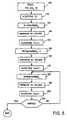
- FIG. 2shows the architecture of a memory device 1 that does not belong to the invention.
- the memory device 1comprises a memory array 2, preferably of flash type, comprising a plurality of data cells 3.
- Memory array 2additionally comprises reference cells 4, used for comparison reading of data cells 3.
- Memory array 2is connected to a memory control unit 5, generally integrated in a single chip with the memory array 2, and comprising address circuits and management circuits of the memory array 2, in a known manner.
- Memory control unit 5additionally comprises a small permanent memory (ROM memory 6), for storing the original reference levels.
- the memory control unit 5is also connected to the exterior through a control unit 7 of a user.
- Figure 3shows a different architecture, wherein some data cells 3 of memory array 2, indicated at 10, store the date of the latest restoration of memory array 2, and some data cells, indicated at 11, store the original threshold voltages corresponding to the various preset digital levels.
- memory control unit 5dispenses with an ROM memory for the original threshold voltages.
- memory control unit 5 of figures 2 and 3begins a test regarding the need to carry out memory refreshing or restoration, at switching on, as described in detail hereinafter.
- memory control unit 5upon switching on (block 20), checks whether it is necessary to carry out refreshing, for example according to the method shown in figure 4b, block 21.
- memory control unit 5requests from the exterior (for example from user control unit 7) the current date DATT, and reads from data cells 10 the stored date DMEM of the latest refreshing or programming, block 23. Memory control unit 5 then checks whether the difference between the current date DATT and the stored date DMEM is equal to, or greater than, a predetermined threshold value K1 (for example 5 years), block 24.
- a predetermined threshold value K1for example 5 years
- memory control unit 5reads the current threshold voltage RIFATT of reference cells 4 and the original threshold voltage RIFMEM from data cells 11 , block 26. Memory control unit 5 then checks whether the difference between the current threshold voltage RIFATT and the stored threshold voltage RIFMEM, is equal to, or greater than, a predetermined threshold value K2, corresponding to the separation between the various levels, block 27.
- the refreshing processbegins with resetting an address counter I, block 32; the threshold voltage THi of the i-th data cell 3, block 33, is then read; threshold voltage THi is compared with threshold value THr corresponding to the level stored in the i-th data cell 3, block 34; if the difference between THi and Thr in absolute value exceeds a predetermined error K3, reprogramming of the i-th cell itself is carried out (block 35).
- the check according to block 34is carried out to take into account any cells originally overprogrammed, which, on completion of the latest programming, had a threshold voltage greater than the reference voltage, and therefore, even after long-term charge losses, have maintained a substantially correct threshold value.
- the following algorithmis based on the fact that when a series of programming voltage pulses with a linearly increasing value is applied to the gate terminal of a nonvolatile cell, at equilibrium, the threshold voltage increases in the same manner as the programming voltage. Reading the present threshold voltage of the cell to be programmed with high precision, once set the increase speed of the cell gate voltage (gradient of the ramp) based on the required threshold voltage value, the time necessary to reach the required value, and thus the number of programming pulses (of constant, predetermined duration) are determined.
- the number of pulsesis calculated from the following equation: N - (V p - V i )/ ⁇ V G wherein N is the number of programming pulses to be applied; V p is the required threshold voltage, V i is the initial (measured) threshold voltage, and ⁇ V G is the amplitude of each programming pulse, set on the basis of the required precision.
- a first sequence of pulsesis initially applied, to bring the cells into an equilibrium condition; a verify step is then carried out, to identify the value of the present cell threshold voltage; the number of pulses necessary to obtain the required threshold value is calculated; a number of pulses close to the number of pulses just calculated is applied, to prevent the cell from being overwritten; the present threshold value is verified out again; the number of pulses necessary to obtain the required threshold value is calculated; the number of pulses just calculated is applied; and a verify step is carried out again, optionally followed by further steps of applying programming and verify pulses.
- the memory control unitreads the data necessary for programming a predetermined data cell 3 of the array.
- the following dataare supplied: the intermediate voltage value V int to which the threshold voltage of the data cell 3 is to be brought to arrive into the linear zone, the amplitude ⁇ V G of the programming pulses, and the required final threshold voltage V p .
- memory control units 5acquires the initial threshold voltage V i corresponding to the just measured value THi for data cell 3, or controls reading of the threshold voltage of reference cell 4 (block 110).
- memory control unit 5calculates the number of pulses N1 necessary to reach the intermediate threshold voltage V int on the basis of (1), and controls that N1 pulses are supplied (block 130). Subsequently, a further verify step is carried out, and the output voltage V eff representing the present threshold voltage of the data cell 3 (block 140) is acquired.
- memory control unit 5calculates the number of pulses N2 necessary to reach the final threshold voltage V p , less one, for safety (block 150) , and controls supplying of the N2 pulses (block 160).
- a further verify stepis then carried out, the value of the present threshold V eff is acquired (block 170), and the number of pulses N3 necessary to reach the final threshold voltage V p is calculated (block 180).
- the N3 pulsesare applied (block 190), and a further verify step is carried out, acquiring the present threshold value V eff (200).
Landscapes
- Engineering & Computer Science (AREA)
- Computer Hardware Design (AREA)
- Read Only Memory (AREA)
Description
- figures 1a and 1b show memory cell distributions,respectively after programming, and after a time close to theretention time;
- figure 2 shows a block diagram of a memory used according toa method that does not belong to the invention;
- figure 3 shows a block diagram of a memory used in anembodiment of the invention;
- figure 4 shows a flow chart of the present method;
- figure 4a show the detail of a block in figure 4,according to an embodiment of the present method;
- figure 4b shows the detail of a block in figure 4, according to an embodiment of the present method; and
- figure 5 shows the detail of two blocks of figure 4.
Claims (4)
- A method for maintaining the memory content of memory cells(3) of a nonvolatile memory (2), the memory cells (3) beingsubjected to long-term charge losses, after a programming step
wherein said memory cells have been programmed to predeterminedthreshold voltage values, comprising the steps of:wherein the step of checking whether said memory cells (3)require refreshing includes the steps of:checking whether said memory cells (3) require refreshing;andrestoring said predetermined threshold voltage values,characterized in that the step of checking whether saidmemory cells (3) require refreshing further includes the stepsof:reading predetermined threshold voltage values;reading present threshold voltage values of said memorycells (3);andin that said predetermined threshold voltage values are readfrom memory locations (11) of said nonvolatile memory (2) where they are stored in digital manner andsaid step of restoring further comprises refreshing said memorylocations (11).determining the difference between said predeterminedthreshold voltage values and said present threshold voltagevalues; andchecking whether said difference exceeds a predeterminedvalue; - A method according to claim 1, wherein said step of checkingwhether said memory cells (3) require refreshing is carried outat switching on of said nonvolatile memory (2).
- A method according to claim 1, for a memory arraycomprising data cells (3) and reference cells (4),characterised in that said step of reading said presentthreshold values comprises the step of reading said referencecells (4).
- A method according to any one of the preceding claims,characterised in that said step of restoring saidpredetermined threshold voltage values comprises the stepsof:determining a present threshold voltage value of onecell (3) of said memory cells;acquiring a predetermined threshold value for said onecell;calculating a first number of programming pulses withregularly increasing amplitude, as necessary to bring saidpresent threshold value to said predetermined threshold value; andapplying a second number of pulses correlated to thefirst number of pulses.
Priority Applications (3)
| Application Number | Priority Date | Filing Date | Title |
|---|---|---|---|
| EP98830536AEP0987715B1 (en) | 1998-09-15 | 1998-09-15 | Method for maintaining the memory of non-volatile memory cells |
| DE69828966TDE69828966D1 (en) | 1998-09-15 | 1998-09-15 | Method for protecting the content of non-volatile memory cells |
| US09/397,387US6169691B1 (en) | 1998-09-15 | 1999-09-15 | Method for maintaining the memory content of non-volatile memory cells |
Applications Claiming Priority (1)
| Application Number | Priority Date | Filing Date | Title |
|---|---|---|---|
| EP98830536AEP0987715B1 (en) | 1998-09-15 | 1998-09-15 | Method for maintaining the memory of non-volatile memory cells |
Publications (2)
| Publication Number | Publication Date |
|---|---|
| EP0987715A1 EP0987715A1 (en) | 2000-03-22 |
| EP0987715B1true EP0987715B1 (en) | 2005-02-09 |
Family
ID=8236784
Family Applications (1)
| Application Number | Title | Priority Date | Filing Date |
|---|---|---|---|
| EP98830536AExpired - LifetimeEP0987715B1 (en) | 1998-09-15 | 1998-09-15 | Method for maintaining the memory of non-volatile memory cells |
Country Status (3)
| Country | Link |
|---|---|
| US (1) | US6169691B1 (en) |
| EP (1) | EP0987715B1 (en) |
| DE (1) | DE69828966D1 (en) |
Families Citing this family (119)
| Publication number | Priority date | Publication date | Assignee | Title |
|---|---|---|---|---|
| IL125604A (en)* | 1997-07-30 | 2004-03-28 | Saifun Semiconductors Ltd | Non-volatile electrically erasable and programmble semiconductor memory cell utilizing asymmetrical charge |
| US6768165B1 (en)* | 1997-08-01 | 2004-07-27 | Saifun Semiconductors Ltd. | Two bit non-volatile electrically erasable and programmable semiconductor memory cell utilizing asymmetrical charge trapping |
| KR100331847B1 (en)* | 1999-06-29 | 2002-04-09 | 박종섭 | Circuit for holding threshold voltage of reference memory cell and method for holding threshold voltage thereby |
| US6396741B1 (en)* | 2000-05-04 | 2002-05-28 | Saifun Semiconductors Ltd. | Programming of nonvolatile memory cells |
| US6928001B2 (en)* | 2000-12-07 | 2005-08-09 | Saifun Semiconductors Ltd. | Programming and erasing methods for a non-volatile memory cell |
| US6396742B1 (en)* | 2000-07-28 | 2002-05-28 | Silicon Storage Technology, Inc. | Testing of multilevel semiconductor memory |
| US6538922B1 (en) | 2000-09-27 | 2003-03-25 | Sandisk Corporation | Writable tracking cells |
| FR2820539B1 (en) | 2001-02-02 | 2003-05-30 | St Microelectronics Sa | METHOD AND DEVICE FOR COOLING REFERENCE CELLS |
| US6584017B2 (en) | 2001-04-05 | 2003-06-24 | Saifun Semiconductors Ltd. | Method for programming a reference cell |
| US6636440B2 (en)* | 2001-04-25 | 2003-10-21 | Saifun Semiconductors Ltd. | Method for operation of an EEPROM array, including refresh thereof |
| US7098107B2 (en)* | 2001-11-19 | 2006-08-29 | Saifun Semiconductor Ltd. | Protective layer in memory device and method therefor |
| US6975536B2 (en)* | 2002-01-31 | 2005-12-13 | Saifun Semiconductors Ltd. | Mass storage array and methods for operation thereof |
| US7190620B2 (en)* | 2002-01-31 | 2007-03-13 | Saifun Semiconductors Ltd. | Method for operating a memory device |
| US6700818B2 (en)* | 2002-01-31 | 2004-03-02 | Saifun Semiconductors Ltd. | Method for operating a memory device |
| US6633500B1 (en)* | 2002-04-26 | 2003-10-14 | Macronix International Co., Ltd. | Systems and methods for refreshing a non-volatile memory using a token |
| US6639839B1 (en)* | 2002-05-21 | 2003-10-28 | Macronix International Co., Ltd. | Sensing method for EEPROM refresh scheme |
| US6917544B2 (en)* | 2002-07-10 | 2005-07-12 | Saifun Semiconductors Ltd. | Multiple use memory chip |
| US6826107B2 (en)* | 2002-08-01 | 2004-11-30 | Saifun Semiconductors Ltd. | High voltage insertion in flash memory cards |
| US6992932B2 (en) | 2002-10-29 | 2006-01-31 | Saifun Semiconductors Ltd | Method circuit and system for read error detection in a non-volatile memory array |
| US6963505B2 (en) | 2002-10-29 | 2005-11-08 | Aifun Semiconductors Ltd. | Method circuit and system for determining a reference voltage |
| US7136304B2 (en) | 2002-10-29 | 2006-11-14 | Saifun Semiconductor Ltd | Method, system and circuit for programming a non-volatile memory array |
| JP4129170B2 (en)* | 2002-12-05 | 2008-08-06 | シャープ株式会社 | Semiconductor memory device and memory data correction method for memory cell |
| US6967896B2 (en)* | 2003-01-30 | 2005-11-22 | Saifun Semiconductors Ltd | Address scramble |
| US7178004B2 (en)* | 2003-01-31 | 2007-02-13 | Yan Polansky | Memory array programming circuit and a method for using the circuit |
| US7142464B2 (en)* | 2003-04-29 | 2006-11-28 | Saifun Semiconductors Ltd. | Apparatus and methods for multi-level sensing in a memory array |
| US7237074B2 (en) | 2003-06-13 | 2007-06-26 | Sandisk Corporation | Tracking cells for a memory system |
| US7123532B2 (en)* | 2003-09-16 | 2006-10-17 | Saifun Semiconductors Ltd. | Operating array cells with matched reference cells |
| US6954393B2 (en)* | 2003-09-16 | 2005-10-11 | Saifun Semiconductors Ltd. | Reading array cell with matched reference cell |
| US7301807B2 (en) | 2003-10-23 | 2007-11-27 | Sandisk Corporation | Writable tracking cells |
| WO2005094178A2 (en)* | 2004-04-01 | 2005-10-13 | Saifun Semiconductors Ltd. | Method, circuit and systems for erasing one or more non-volatile memory cells |
| US7755938B2 (en)* | 2004-04-19 | 2010-07-13 | Saifun Semiconductors Ltd. | Method for reading a memory array with neighbor effect cancellation |
| US7366025B2 (en)* | 2004-06-10 | 2008-04-29 | Saifun Semiconductors Ltd. | Reduced power programming of non-volatile cells |
| US7317633B2 (en) | 2004-07-06 | 2008-01-08 | Saifun Semiconductors Ltd | Protection of NROM devices from charge damage |
| US7095655B2 (en)* | 2004-08-12 | 2006-08-22 | Saifun Semiconductors Ltd. | Dynamic matching of signal path and reference path for sensing |
| US20060068551A1 (en)* | 2004-09-27 | 2006-03-30 | Saifun Semiconductors, Ltd. | Method for embedding NROM |
| US7638850B2 (en) | 2004-10-14 | 2009-12-29 | Saifun Semiconductors Ltd. | Non-volatile memory structure and method of fabrication |
| US20060146624A1 (en)* | 2004-12-02 | 2006-07-06 | Saifun Semiconductors, Ltd. | Current folding sense amplifier |
| US7535765B2 (en) | 2004-12-09 | 2009-05-19 | Saifun Semiconductors Ltd. | Non-volatile memory device and method for reading cells |
| US7257025B2 (en)* | 2004-12-09 | 2007-08-14 | Saifun Semiconductors Ltd | Method for reading non-volatile memory cells |
| EP1686592A3 (en)* | 2005-01-19 | 2007-04-25 | Saifun Semiconductors Ltd. | Partial erase verify |
| US8053812B2 (en) | 2005-03-17 | 2011-11-08 | Spansion Israel Ltd | Contact in planar NROM technology |
| US20070141788A1 (en)* | 2005-05-25 | 2007-06-21 | Ilan Bloom | Method for embedding non-volatile memory with logic circuitry |
| US8400841B2 (en)* | 2005-06-15 | 2013-03-19 | Spansion Israel Ltd. | Device to program adjacent storage cells of different NROM cells |
| US7184313B2 (en)* | 2005-06-17 | 2007-02-27 | Saifun Semiconductors Ltd. | Method circuit and system for compensating for temperature induced margin loss in non-volatile memory cells |
| US7786512B2 (en)* | 2005-07-18 | 2010-08-31 | Saifun Semiconductors Ltd. | Dense non-volatile memory array and method of fabrication |
| US20070036007A1 (en)* | 2005-08-09 | 2007-02-15 | Saifun Semiconductors, Ltd. | Sticky bit buffer |
| US7668017B2 (en) | 2005-08-17 | 2010-02-23 | Saifun Semiconductors Ltd. | Method of erasing non-volatile memory cells |
| US20070096199A1 (en)* | 2005-09-08 | 2007-05-03 | Eli Lusky | Method of manufacturing symmetric arrays |
| US7221138B2 (en) | 2005-09-27 | 2007-05-22 | Saifun Semiconductors Ltd | Method and apparatus for measuring charge pump output current |
| US20070120180A1 (en)* | 2005-11-25 | 2007-05-31 | Boaz Eitan | Transition areas for dense memory arrays |
| US7352627B2 (en)* | 2006-01-03 | 2008-04-01 | Saifon Semiconductors Ltd. | Method, system, and circuit for operating a non-volatile memory array |
| US7808818B2 (en)* | 2006-01-12 | 2010-10-05 | Saifun Semiconductors Ltd. | Secondary injection for NROM |
| US20070173017A1 (en)* | 2006-01-20 | 2007-07-26 | Saifun Semiconductors, Ltd. | Advanced non-volatile memory array and method of fabrication thereof |
| US7760554B2 (en)* | 2006-02-21 | 2010-07-20 | Saifun Semiconductors Ltd. | NROM non-volatile memory and mode of operation |
| US8253452B2 (en)* | 2006-02-21 | 2012-08-28 | Spansion Israel Ltd | Circuit and method for powering up an integrated circuit and an integrated circuit utilizing same |
| US7692961B2 (en)* | 2006-02-21 | 2010-04-06 | Saifun Semiconductors Ltd. | Method, circuit and device for disturb-control of programming nonvolatile memory cells by hot-hole injection (HHI) and by channel hot-electron (CHE) injection |
| US7638835B2 (en) | 2006-02-28 | 2009-12-29 | Saifun Semiconductors Ltd. | Double density NROM with nitride strips (DDNS) |
| US20070255889A1 (en)* | 2006-03-22 | 2007-11-01 | Yoav Yogev | Non-volatile memory device and method of operating the device |
| US7590600B2 (en)* | 2006-03-28 | 2009-09-15 | Microsoft Corporation | Self-contained rights management for non-volatile memory |
| KR100784107B1 (en) | 2006-04-24 | 2007-12-10 | 주식회사 하이닉스반도체 | Driving method of flash memory device |
| US7701779B2 (en)* | 2006-04-27 | 2010-04-20 | Sajfun Semiconductors Ltd. | Method for programming a reference cell |
| KR101202537B1 (en) | 2006-05-12 | 2012-11-19 | 애플 인크. | Combined distortion estimation and error correction coding for memory devices |
| WO2007132453A2 (en) | 2006-05-12 | 2007-11-22 | Anobit Technologies Ltd. | Distortion estimation and cancellation in memory devices |
| WO2007132456A2 (en) | 2006-05-12 | 2007-11-22 | Anobit Technologies Ltd. | Memory device with adaptive capacity |
| US7605579B2 (en)* | 2006-09-18 | 2009-10-20 | Saifun Semiconductors Ltd. | Measuring and controlling current consumption and output current of charge pumps |
| KR100875292B1 (en)* | 2006-09-19 | 2008-12-23 | 삼성전자주식회사 | Flash memory device and its refresh method |
| US7975192B2 (en) | 2006-10-30 | 2011-07-05 | Anobit Technologies Ltd. | Reading memory cells using multiple thresholds |
| WO2008068747A2 (en) | 2006-12-03 | 2008-06-12 | Anobit Technologies Ltd. | Automatic defect management in memory devices |
| US8151166B2 (en)* | 2007-01-24 | 2012-04-03 | Anobit Technologies Ltd. | Reduction of back pattern dependency effects in memory devices |
| US8369141B2 (en) | 2007-03-12 | 2013-02-05 | Apple Inc. | Adaptive estimation of memory cell read thresholds |
| US20080239599A1 (en)* | 2007-04-01 | 2008-10-02 | Yehuda Yizraeli | Clamping Voltage Events Such As ESD |
| WO2008139441A2 (en)* | 2007-05-12 | 2008-11-20 | Anobit Technologies Ltd. | Memory device with internal signal processing unit |
| US8234545B2 (en) | 2007-05-12 | 2012-07-31 | Apple Inc. | Data storage with incremental redundancy |
| US8259497B2 (en)* | 2007-08-06 | 2012-09-04 | Apple Inc. | Programming schemes for multi-level analog memory cells |
| US8174905B2 (en) | 2007-09-19 | 2012-05-08 | Anobit Technologies Ltd. | Programming orders for reducing distortion in arrays of multi-level analog memory cells |
| US8527819B2 (en) | 2007-10-19 | 2013-09-03 | Apple Inc. | Data storage in analog memory cell arrays having erase failures |
| US8270246B2 (en) | 2007-11-13 | 2012-09-18 | Apple Inc. | Optimized selection of memory chips in multi-chips memory devices |
| US8225181B2 (en)* | 2007-11-30 | 2012-07-17 | Apple Inc. | Efficient re-read operations from memory devices |
| US8209588B2 (en) | 2007-12-12 | 2012-06-26 | Anobit Technologies Ltd. | Efficient interference cancellation in analog memory cell arrays |
| US8456905B2 (en)* | 2007-12-16 | 2013-06-04 | Apple Inc. | Efficient data storage in multi-plane memory devices |
| US8938655B2 (en)* | 2007-12-20 | 2015-01-20 | Spansion Llc | Extending flash memory data retension via rewrite refresh |
| US8156398B2 (en) | 2008-02-05 | 2012-04-10 | Anobit Technologies Ltd. | Parameter estimation based on error correction code parity check equations |
| US8230300B2 (en) | 2008-03-07 | 2012-07-24 | Apple Inc. | Efficient readout from analog memory cells using data compression |
| US8400858B2 (en) | 2008-03-18 | 2013-03-19 | Apple Inc. | Memory device with reduced sense time readout |
| US7821839B2 (en)* | 2008-06-27 | 2010-10-26 | Sandisk Il Ltd. | Gain control for read operations in flash memory |
| US8498151B1 (en) | 2008-08-05 | 2013-07-30 | Apple Inc. | Data storage in analog memory cells using modified pass voltages |
| US8949684B1 (en) | 2008-09-02 | 2015-02-03 | Apple Inc. | Segmented data storage |
| US8169825B1 (en) | 2008-09-02 | 2012-05-01 | Anobit Technologies Ltd. | Reliable data storage in analog memory cells subjected to long retention periods |
| US8482978B1 (en) | 2008-09-14 | 2013-07-09 | Apple Inc. | Estimation of memory cell read thresholds by sampling inside programming level distribution intervals |
| US8239734B1 (en) | 2008-10-15 | 2012-08-07 | Apple Inc. | Efficient data storage in storage device arrays |
| US8713330B1 (en) | 2008-10-30 | 2014-04-29 | Apple Inc. | Data scrambling in memory devices |
| US8208304B2 (en) | 2008-11-16 | 2012-06-26 | Anobit Technologies Ltd. | Storage at M bits/cell density in N bits/cell analog memory cell devices, M>N |
| DE112008004246B4 (en)* | 2008-12-30 | 2018-11-15 | Micron Technology, Inc. | Temperature alarm and low-rate refresh for nonvolatile memory |
| US8174857B1 (en) | 2008-12-31 | 2012-05-08 | Anobit Technologies Ltd. | Efficient readout schemes for analog memory cell devices using multiple read threshold sets |
| US8248831B2 (en) | 2008-12-31 | 2012-08-21 | Apple Inc. | Rejuvenation of analog memory cells |
| US8924661B1 (en) | 2009-01-18 | 2014-12-30 | Apple Inc. | Memory system including a controller and processors associated with memory devices |
| US8223551B2 (en)* | 2009-02-19 | 2012-07-17 | Micron Technology, Inc. | Soft landing for desired program threshold voltage |
| US8228701B2 (en)* | 2009-03-01 | 2012-07-24 | Apple Inc. | Selective activation of programming schemes in analog memory cell arrays |
| US8832354B2 (en) | 2009-03-25 | 2014-09-09 | Apple Inc. | Use of host system resources by memory controller |
| US8259506B1 (en) | 2009-03-25 | 2012-09-04 | Apple Inc. | Database of memory read thresholds |
| US8238157B1 (en) | 2009-04-12 | 2012-08-07 | Apple Inc. | Selective re-programming of analog memory cells |
| JP5359570B2 (en)* | 2009-06-03 | 2013-12-04 | 富士通株式会社 | Memory test control apparatus and memory test control method |
| US8479080B1 (en) | 2009-07-12 | 2013-07-02 | Apple Inc. | Adaptive over-provisioning in memory systems |
| US8495465B1 (en) | 2009-10-15 | 2013-07-23 | Apple Inc. | Error correction coding over multiple memory pages |
| US8677054B1 (en) | 2009-12-16 | 2014-03-18 | Apple Inc. | Memory management schemes for non-volatile memory devices |
| US8694814B1 (en) | 2010-01-10 | 2014-04-08 | Apple Inc. | Reuse of host hibernation storage space by memory controller |
| US8572311B1 (en) | 2010-01-11 | 2013-10-29 | Apple Inc. | Redundant data storage in multi-die memory systems |
| US8694853B1 (en) | 2010-05-04 | 2014-04-08 | Apple Inc. | Read commands for reading interfering memory cells |
| US8572423B1 (en) | 2010-06-22 | 2013-10-29 | Apple Inc. | Reducing peak current in memory systems |
| US8595591B1 (en) | 2010-07-11 | 2013-11-26 | Apple Inc. | Interference-aware assignment of programming levels in analog memory cells |
| US9104580B1 (en) | 2010-07-27 | 2015-08-11 | Apple Inc. | Cache memory for hybrid disk drives |
| US8645794B1 (en) | 2010-07-31 | 2014-02-04 | Apple Inc. | Data storage in analog memory cells using a non-integer number of bits per cell |
| US8856475B1 (en) | 2010-08-01 | 2014-10-07 | Apple Inc. | Efficient selection of memory blocks for compaction |
| US8694854B1 (en) | 2010-08-17 | 2014-04-08 | Apple Inc. | Read threshold setting based on soft readout statistics |
| US9021181B1 (en) | 2010-09-27 | 2015-04-28 | Apple Inc. | Memory management for unifying memory cell conditions by using maximum time intervals |
| US9236132B2 (en) | 2013-06-04 | 2016-01-12 | Apple Inc. | Mitigating reliability degradation of analog memory cells during long static and erased state retention |
| KR20170090357A (en)* | 2016-01-28 | 2017-08-07 | 가부시키가이샤 한도오따이 에네루기 켄큐쇼 | Method for operating the semiconductor device |
| US11556416B2 (en) | 2021-05-05 | 2023-01-17 | Apple Inc. | Controlling memory readout reliability and throughput by adjusting distance between read thresholds |
| US11847342B2 (en) | 2021-07-28 | 2023-12-19 | Apple Inc. | Efficient transfer of hard data and confidence levels in reading a nonvolatile memory |
Family Cites Families (5)
| Publication number | Priority date | Publication date | Assignee | Title |
|---|---|---|---|---|
| US4218764A (en)* | 1978-10-03 | 1980-08-19 | Matsushita Electric Industrial Co., Ltd. | Non-volatile memory refresh control circuit |
| KR100473308B1 (en)* | 1995-01-31 | 2005-03-14 | 가부시끼가이샤 히다치 세이사꾸쇼 | Nonvolatile memory device |
| JP3562043B2 (en)* | 1995-07-19 | 2004-09-08 | ソニー株式会社 | Non-volatile storage device |
| FR2745114B1 (en)* | 1996-02-20 | 1998-04-17 | Sgs Thomson Microelectronics | NON-VOLATILE ELECTRICALLY MODIFIABLE MEMORY WITH SELF-CONTAINED COOLING |
| US5852582A (en)* | 1997-02-18 | 1998-12-22 | Advanced Micro Devices, Inc. | Non-volatile storage device refresh time detector |
- 1998
- 1998-09-15EPEP98830536Apatent/EP0987715B1/ennot_activeExpired - Lifetime
- 1998-09-15DEDE69828966Tpatent/DE69828966D1/ennot_activeExpired - Lifetime
- 1999
- 1999-09-15USUS09/397,387patent/US6169691B1/ennot_activeExpired - Lifetime
Also Published As
| Publication number | Publication date |
|---|---|
| US6169691B1 (en) | 2001-01-02 |
| EP0987715A1 (en) | 2000-03-22 |
| DE69828966D1 (en) | 2005-03-17 |
Similar Documents
| Publication | Publication Date | Title |
|---|---|---|
| EP0987715B1 (en) | Method for maintaining the memory of non-volatile memory cells | |
| US7310270B2 (en) | Nonvolatile semiconductor memory device | |
| JP3941149B2 (en) | Semiconductor nonvolatile memory device | |
| KR100841980B1 (en) | Method of erasing flash memory device to improve scattering of erased cells | |
| US8345487B2 (en) | Method of setting read voltage minimizing read data errors | |
| US7437631B2 (en) | Soft errors handling in EEPROM devices | |
| US7903467B2 (en) | Programming method of multi-bit flash memory device for reducing programming error | |
| US20070086244A1 (en) | Data restoration in case of page-programming failure | |
| EP0685852A2 (en) | Memory system and method of using same | |
| US20060242485A1 (en) | Error detection, documentation, and correction in a flash memory device | |
| JP2004185745A (en) | Semiconductor memory device and reference cell correction method | |
| KR950009731A (en) | Nonvolatile Semiconductor Memory | |
| WO1996018193A1 (en) | Flash memory having adaptive sensing and method | |
| WO2001063613A1 (en) | Multilevel cell programming | |
| KR20080080511A (en) | Method and apparatus for programming / deleting nonvolatile memory | |
| EP2704150A2 (en) | Non-volatile memory (NVM) that uses soft programming | |
| JP3850791B2 (en) | Nonvolatile semiconductor memory device | |
| US20040015649A1 (en) | Circuit for supplying program/erase voltages in flash memory device | |
| US6128224A (en) | Method and apparatus for writing an erasable non-volatile memory | |
| CN110473584B (en) | Method for re-verifying erased block in solid state storage device | |
| US7289368B2 (en) | Control of voltages during erase and re-program operations of memory cells | |
| US20100332898A1 (en) | Nonvolatile memory device and copyback program method thereof | |
| EP1782426B1 (en) | Self-adaptive program delay circuitry for programmable memories | |
| KR19990042162A (en) | Nonvolatile Memory Device And Its Program Method | |
| KR20100034613A (en) | Method for programming charge trap flash memory device |
Legal Events
| Date | Code | Title | Description |
|---|---|---|---|
| PUAI | Public reference made under article 153(3) epc to a published international application that has entered the european phase | Free format text:ORIGINAL CODE: 0009012 | |
| AK | Designated contracting states | Kind code of ref document:A1 Designated state(s):DE FR GB IT | |
| AX | Request for extension of the european patent | Free format text:AL;LT;LV;MK;RO;SI | |
| K1C3 | Correction of patent application (complete document) published | Effective date:20000322 | |
| 17P | Request for examination filed | Effective date:20000912 | |
| AKX | Designation fees paid | Free format text:DE FR GB IT | |
| 17Q | First examination report despatched | Effective date:20040120 | |
| GRAP | Despatch of communication of intention to grant a patent | Free format text:ORIGINAL CODE: EPIDOSNIGR1 | |
| GRAS | Grant fee paid | Free format text:ORIGINAL CODE: EPIDOSNIGR3 | |
| GRAA | (expected) grant | Free format text:ORIGINAL CODE: 0009210 | |
| AK | Designated contracting states | Kind code of ref document:B1 Designated state(s):DE FR GB IT | |
| REG | Reference to a national code | Ref country code:GB Ref legal event code:FG4D | |
| REF | Corresponds to: | Ref document number:69828966 Country of ref document:DE Date of ref document:20050317 Kind code of ref document:P | |
| PG25 | Lapsed in a contracting state [announced via postgrant information from national office to epo] | Ref country code:DE Free format text:LAPSE BECAUSE OF FAILURE TO SUBMIT A TRANSLATION OF THE DESCRIPTION OR TO PAY THE FEE WITHIN THE PRESCRIBED TIME-LIMIT Effective date:20050510 | |
| PG25 | Lapsed in a contracting state [announced via postgrant information from national office to epo] | Ref country code:GB Free format text:LAPSE BECAUSE OF NON-PAYMENT OF DUE FEES Effective date:20050915 | |
| PLBE | No opposition filed within time limit | Free format text:ORIGINAL CODE: 0009261 | |
| STAA | Information on the status of an ep patent application or granted ep patent | Free format text:STATUS: NO OPPOSITION FILED WITHIN TIME LIMIT | |
| 26N | No opposition filed | Effective date:20051110 | |
| ET | Fr: translation filed | ||
| GBPC | Gb: european patent ceased through non-payment of renewal fee | Effective date:20050915 | |
| PGFP | Annual fee paid to national office [announced via postgrant information from national office to epo] | Ref country code:IT Payment date:20070913 Year of fee payment:10 | |
| PGFP | Annual fee paid to national office [announced via postgrant information from national office to epo] | Ref country code:FR Payment date:20080929 Year of fee payment:11 | |
| PG25 | Lapsed in a contracting state [announced via postgrant information from national office to epo] | Ref country code:IT Free format text:LAPSE BECAUSE OF NON-PAYMENT OF DUE FEES Effective date:20080915 | |
| REG | Reference to a national code | Ref country code:FR Ref legal event code:ST Effective date:20100531 | |
| PG25 | Lapsed in a contracting state [announced via postgrant information from national office to epo] | Ref country code:FR Free format text:LAPSE BECAUSE OF NON-PAYMENT OF DUE FEES Effective date:20090930 |