EP0985289B1 - Optical multiplexing and demultiplexing - Google Patents
Optical multiplexing and demultiplexingDownload PDFInfo
- Publication number
- EP0985289B1 EP0985289B1EP98922822AEP98922822AEP0985289B1EP 0985289 B1EP0985289 B1EP 0985289B1EP 98922822 AEP98922822 AEP 98922822AEP 98922822 AEP98922822 AEP 98922822AEP 0985289 B1EP0985289 B1EP 0985289B1
- Authority
- EP
- European Patent Office
- Prior art keywords
- ports
- input
- port
- group
- output
- Prior art date
- Legal status (The legal status is an assumption and is not a legal conclusion. Google has not performed a legal analysis and makes no representation as to the accuracy of the status listed.)
- Expired - Lifetime
Links
- 230000003287optical effectEffects0.000titleclaimsdescription41
- 238000000034methodMethods0.000claimsdescription12
- 239000000835fiberSubstances0.000description27
- 230000008878couplingEffects0.000description7
- 238000010168coupling processMethods0.000description7
- 238000005859coupling reactionMethods0.000description7
- 230000005540biological transmissionEffects0.000description4
- 230000003595spectral effectEffects0.000description4
- 239000013307optical fiberSubstances0.000description3
- 238000000926separation methodMethods0.000description3
- 238000001228spectrumMethods0.000description2
- 239000000758substrateSubstances0.000description2
- VYPSYNLAJGMNEJ-UHFFFAOYSA-NSilicium dioxideChemical compoundO=[Si]=OVYPSYNLAJGMNEJ-UHFFFAOYSA-N0.000description1
- XUIMIQQOPSSXEZ-UHFFFAOYSA-NSiliconChemical compound[Si]XUIMIQQOPSSXEZ-UHFFFAOYSA-N0.000description1
- 239000006185dispersionSubstances0.000description1
- 238000005516engineering processMethods0.000description1
- 239000011521glassSubstances0.000description1
- 230000000737periodic effectEffects0.000description1
- 230000001902propagating effectEffects0.000description1
- 229910052710siliconInorganic materials0.000description1
- 239000010703siliconSubstances0.000description1
Images


Classifications
- G—PHYSICS
- G02—OPTICS
- G02B—OPTICAL ELEMENTS, SYSTEMS OR APPARATUS
- G02B6/00—Light guides; Structural details of arrangements comprising light guides and other optical elements, e.g. couplings
- G02B6/10—Light guides; Structural details of arrangements comprising light guides and other optical elements, e.g. couplings of the optical waveguide type
- G02B6/12—Light guides; Structural details of arrangements comprising light guides and other optical elements, e.g. couplings of the optical waveguide type of the integrated circuit kind
- G02B6/12007—Light guides; Structural details of arrangements comprising light guides and other optical elements, e.g. couplings of the optical waveguide type of the integrated circuit kind forming wavelength selective elements, e.g. multiplexer, demultiplexer
- G02B6/12009—Light guides; Structural details of arrangements comprising light guides and other optical elements, e.g. couplings of the optical waveguide type of the integrated circuit kind forming wavelength selective elements, e.g. multiplexer, demultiplexer comprising arrayed waveguide grating [AWG] devices, i.e. with a phased array of waveguides
- G02B6/12019—Light guides; Structural details of arrangements comprising light guides and other optical elements, e.g. couplings of the optical waveguide type of the integrated circuit kind forming wavelength selective elements, e.g. multiplexer, demultiplexer comprising arrayed waveguide grating [AWG] devices, i.e. with a phased array of waveguides characterised by the optical interconnection to or from the AWG devices, e.g. integration or coupling with lasers or photodiodes
- G02B6/12021—Comprising cascaded AWG devices; AWG multipass configuration; Plural AWG devices integrated on a single chip
- H—ELECTRICITY
- H04—ELECTRIC COMMUNICATION TECHNIQUE
- H04J—MULTIPLEX COMMUNICATION
- H04J14/00—Optical multiplex systems
- H04J14/02—Wavelength-division multiplex systems
- H04J14/03—WDM arrangements
- H04J14/0305—WDM arrangements in end terminals
- H—ELECTRICITY
- H04—ELECTRIC COMMUNICATION TECHNIQUE
- H04Q—SELECTING
- H04Q11/00—Selecting arrangements for multiplex systems
- H04Q11/0001—Selecting arrangements for multiplex systems using optical switching
- H04Q11/0003—Details
- H—ELECTRICITY
- H04—ELECTRIC COMMUNICATION TECHNIQUE
- H04Q—SELECTING
- H04Q11/00—Selecting arrangements for multiplex systems
- H04Q11/0001—Selecting arrangements for multiplex systems using optical switching
- H04Q11/0005—Switch and router aspects
- H04Q2011/0007—Construction
- H04Q2011/0022—Construction using fibre gratings
- H—ELECTRICITY
- H04—ELECTRIC COMMUNICATION TECHNIQUE
- H04Q—SELECTING
- H04Q11/00—Selecting arrangements for multiplex systems
- H04Q11/0001—Selecting arrangements for multiplex systems using optical switching
- H04Q11/0005—Switch and router aspects
- H04Q2011/0037—Operation
- H04Q2011/0049—Crosstalk reduction; Noise; Power budget
Definitions
- the inventiongenerally relates to optical transmission systems employing wavelength division multiplexing, and particularly to a so-called waveguide phased array component used therein to carry out multiplexing and demultiplexing of the optical signal.
- Wavelength Division Multiplexingrepresents an efficient way to increase manyfold the capacity of an optical fiber.
- a number of independent transmitter-receiver pairsuse the same fiber.
- the principle of WDMis illustrated in Figures 1a and 1b by using a system comprising four parallel transmitter-receiver pairs as an example.
- Each of the four information sources(not shown in the figure) modulates one of the four optical transmitters each of which produces light at a different wavelength ( ⁇ 1 ... ⁇ 4 ).
- the modulation bandwidth of each sourceis narrower than the separation between the wavelengths, resulting in that the spectra of the modulated signals do not overlap.
- the signals produced by the transmittersare combined into the same optical fiber OF in a WDM multiplexer WDM1, which is an entirely optical (and often passive) component.
- WDM demultiplexer WDM2also an entirely optical (and often passive) component, separates the different spectral components of the combined signal from each other.
- Each of these signalsis detected by a different receiver.
- each signalis assigned a narrow wavelength window in a specific wavelength range.
- a typical practical examplecould then be a system where the signals are in the 1550 nm wavelength range, e.g.
- the de facto standard for wavelength separationis a multiple of 100 GHz (appr. 0.8 nm).
- the waveguide phased array component(also known as waveguide array grating or arrayed waveguide grating) is a known component in fiber optics, most suitable for systems employing wavelength division multiplexing due to e.g. the fact that a large number of wavelengths can be transferred over it, such as a WDM signal comprising 16 or 32 wavelengths.
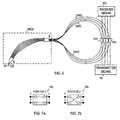
- Figure 2illustrates the structure of a waveguide phased array component WGA.
- the componentcomprises, integrated on the same substrate, N optical input/output guides AWG on the first side of the component, N optical input/output guides BWG on the second side of the component, two slab waveguides SWG1 and SWG2, and a grating GR constituted by optical channel waveguides WG, the grating GR connecting the slab waveguides to one another.
- Both sides of the componentmay act as the input or output side, whereby the waveguides AWG and BWG may be output or input guides.
- the slab waveguideswhich connect input/output guides to separate channel waveguides WG in the grating, restrict propagation of light only in the plane perpendicular to the substrate but allow light propagation to the sides.
- the channel waveguides in the gratinginstead, prevent light propagation also to the sides.
- the channel waveguides that connect to the slab waveguides on both sidesare arranged on a circular arc so that each of them is directed towards the center waveguide of the waveguide group on the opposite side.
- a constant difference in lengthexists between two adjacent channel waveguides in the grating, the difference in length being a multiple of the center wavelength used.
- the lightis distributed to all the waveguides of the grating.
- the difference in length of the waveguidesis a multiple of the center wavelength, all the waves are in the same phase upon arriving in the output slab waveguide whereupon the light is focused to the center output waveguide.
- the wave front arriving in the outputis slightly tilted, which means that it is not focused exactly at the center but at another waveguide of the output side.
- the componentfocuses different wavelengths to different outputs, the dimensioning of the component determining which wavelengths are focused on which output.
- the wavelength of the center input waveguidedetermines which the output waveguide is, the location of the input waveguide determines which the output waveguide is.
- the waveguide phased array componentthus comprises a number of light channels whose geometry defines that they have both focusing characteristics (a lens) and dispersing characteristics (the wavelength dependency of the grating).
- Figure 3illustrates the basic operational principle of the component in association with a case in which three different wavelengths ( ⁇ 1 , ⁇ 2 , ⁇ 3 ) are used to couple light alternately to each of the three input ports.
- the output port of a specific wavelength channeldepends both on the wavelength of the channel in question and which the input port of the channel in question is.
- the componentis capable of demultiplexing N wavelength channels received from one input port so that each of the channels goes to a different output port. How the channels are distributed among the output ports depends on which the input port is. Examined from the network point of view, a situation thus exists in which a network element connected to a specific output port and receiving a signal at a specific wavelength knows, based on the output port and the wavelength, from which input port the signal originates.
- a symmetrical N ⁇ N phased array componenthas N optical ports on the A-side and N optical ports on the B-side.
- the componenthas been so designed that it multiplexes wavelengths whose separation is ⁇ .
- istands for the port sequence number on the A-side and j for the port sequence number on the B-side
- the wavelength coupled between two portsis the same regardless of whether light is input to the A-side port and output from the B-side port or in the opposite direction, and the operation of the component is also in other respects symmetric as regards changes of the A- and B-sides.
- Nis the number of ports on the side which has the majority, and the other side may simply be seen as lacking some ports, but the coupling between the ports is nevertheless described by the above formula.
- the basic function of the component as a demultiplexeris illustrated as the wavelengths coupling from one A-side port to all the B-side ports so that a dedicated wavelength is coupled to each of them.
- a reverse operation as a multiplexeris obtained when a wavelength is input to each A-side port, the wavelengths being selected so that all wavelengths are coupled out of the same B-side port.
- the operation of the componentis periodic also with respect to wavelength, the period between the wavelengths being the Free Spectral Range (FSR).
- FSRFree Spectral Range
- a couplingexists between two ports at the wavelength ⁇
- a couplingalso exists between them at the wavelengths ⁇ + n ⁇ FSR, where n is a positive or negative integer.
- the components used in practiceare planned so that FSR is larger than ⁇ N because otherwise the same wavelength couples from a specific input port to more than one output port, which is undesirable.
- a special caseis an N ⁇ N phased array where FSR equals ⁇ N exactly.
- N-1 wavelengthsare separated to the output fibers.
- EP0591042discloses an optical device for multiplexing and demultiplexing optical signals in looped optical paths, consisting of a plurality of individual loop-back optical paths.
- the deviceis a multi/demultiplexer having an arrayed waveguide grating disposed between a plurality of input sections and output sections which are joined by the plurality of individual loop-back optical paths.
- US5488680discloses an optical apparatus that includes a first frequency routing device having at least one input port and P output ports, where P>2.
- a second frequency routing deviceis also provided that has P input ports and at least one output port. P optical paths couple the input port of the first frequency routing device to the output port of the second frequency routing device.
- WO9804944discloses an optical multiplexer/demultiplexer where an improved spectral characteristic is provided by two diffraction gratings that are arranged optically in tandem.
- the gratingsare arranged so to provide free spectral ranges differing by a factor of at least two, and have a coupling between them that carries over into the second grating information concerning the dispersion afforded by the first grating.
- This solutionprovides the advantage that the same wavelengths present in the multiplexing and demultiplexing pass the component in opposite directions, which considerably reduces crosstalk between two signals at the same wavelength.
- the problem of this solutionis that crosstalk takes place between different wavelengths passing through the component in the same direction, particularly between adjacent wavelengths coupled to adjacent ports.
- the object of the inventionis to obviate the above drawbacks and to obtain a solution by means of which crosstalk can be minimized both between two signals at the same wavelength and between different wavelengths passing through the component.
- the idea of the inventionis to carry out the multiplexer and demultiplexer functions so that the signals being multiplexed and demultiplexed propagate through the component in opposite directions and, further, alternately couple to ports of one end.
- crosstalkcan be reduced (a) between same wavelengths because mutually identical wavelengths propagate in opposite directions, and additionally (b) between adjacent wavelengths because light propagates in opposite directions in adjacent ports.
- the inventive solutionprovides the further advantage that multiplexing and demultiplexing can be carried out economically, because these functions can be carried out with the same component.
- the multiplexer and demultiplexer functionsare carried out as illustrated by the example of Figure 5 .
- the input fiber IFD of the demultiplexer functionis connected to an A-side port of the waveguide phased array component.
- the output fibers of the demultiplexer function, of which there are N/2are connected to even ports on the B-side. In such a case, N/2 different wavelengths are separated to the output ports.
- the input fibers of the multiplexer function, of which there are N/2 also,are connected to the free, odd B-side ports whereby the same N/2 different wavelengths that were demultiplexed are multiplexed to the fiber OFM connected to the A-side port (adjacent port to the one to which the fiber IFD is connected).
- the ports on the B-sideare divided into two groups; the first group consisting of the demultiplexer function output ports (illustrated with outgoing arrows), and a second group consisting of the multiplexer function input ports (illustrated with incoming arrows).
- the portsmay naturally be assigned to the groups in an opposite order, so that the demultiplexer output fibers are connected to the odd ports on the B-side and the multiplexer function input fibers to even ports. Light thus propagates into opposite directions in adjacent ports on the B-side.
- An advantageous use for the component implemented according to the inventionis an add/drop device or filter in an optical network.
- the function of an optical add/drop filteris (1) to guide a preselected narrowband channel (wavelength) out of the optical WDM signal that propagates in the fiber coming to the filter (drop function), and/or (2) to add a preselected narrowband channel to the fiber leaving the filter (add function).
- Signals (wavelengths) that have not been selected to be droppedpass the add/drop filter from the input fiber to the output fiber. With the filter, then, the desired narrowband channel is added or dropped without influencing the spectrum of the optical WDM signal in any other way.
- an add/drop deviceis a network element that can be configured so that the wavelengths to be dropped/added can be chosen.
- Figure 6illustrates an add/drop device that is based on the inventive solution in which the waveguides of the component are connected to the ports according to the principle of Figure 5 .
- the devicehas two ports on the A-side, one of these being the input port IG (to which the input fiber is connected) and the second being the output port (to which the output fiber is connected).
- Nbeing an even integer
- These output ports(aforementioned first group) are in this example the B-side odd ports, and the multiplexer input ports (aforementioned second group) are the B-side even ports.
- Ports in the first and second group, corresponding to a specific wavelength, form a pair of ports, and for each of such pairs the device has an optical 2x2 switch (2 inputs and 2 outputs) SW i (i1...N/2).
- An optical waveguide OWGis connected from a port belonging to the first group (demultiplexer output port) in the pair of ports to the first input of the optical switch corresponding to the pair in question.
- a transmitter means TSthat generates the wavelength channel to be added.
- the first output of the switchis connected to a port belonging to the second group (multiplexer input port) in the pair of ports in question, and the second output is connected to a receiving means RS, used to receive the dropped wavelength channel.
- Each switchhas a through connection position according to Figure 7a , in which the switch connects the first input R to the first output T, and the second input S to the second output U, and a cross-connection position according to Figure 7b , in which the switch connects the first input R to the second output U, and the second input S to the first output T.
- the switchesare known optical switches, for example electromechanical switches. Such switches are manufactured e.g. by JDS FITEL Inc., Canada. It should be noted that the switches do not necessarily need to be 2 ⁇ 2 switches, as the same functions can be constructed from larger switches. The size of the switches is consequently not an issue, as long as they operate as described above.
- Two links according to Figure 1bmay also exist in parallel, with operation in opposite directions. In such a case, both ends require multiplexer and demultiplexer functions, which may be incorporated in the same component in accordance with the invention.
- the waveguide phased array component operating as described aboveis dimensioned as in prior art and manufactured by a prior art method, for example by planar fiber-optic technique using e.g. doped glass light channels that are manufactured on either silicon wafer or quartz glass wafer.
- the demultiplexer function output and the multiplexer function inputdo not necessarily have to be in adjacent ports, but an empty port may be left between them. It is essential, however, that the demultiplexer function outputs and the multiplexer function inputs on the second side (B-side) occur alternately, whereby two adjacent ports will not have signals propagating in the same direction.
- the componentmay also have empty ports on the A-side. The essential issue is that one of the ports acts as the input port and one as the output port. In other words, the inventive component may be implemented as part of a larger component.
Landscapes
- Engineering & Computer Science (AREA)
- Computer Networks & Wireless Communication (AREA)
- Physics & Mathematics (AREA)
- Signal Processing (AREA)
- Microelectronics & Electronic Packaging (AREA)
- General Physics & Mathematics (AREA)
- Optics & Photonics (AREA)
- Optical Integrated Circuits (AREA)
- Optical Communication System (AREA)
Description
- The invention generally relates to optical transmission systems employing wavelength division multiplexing, and particularly to a so-called waveguide phased array component used therein to carry out multiplexing and demultiplexing of the optical signal.
- Wavelength Division Multiplexing (WDM) represents an efficient way to increase manyfold the capacity of an optical fiber. In wavelength division multiplexing, a number of independent transmitter-receiver pairs use the same fiber. The principle of WDM is illustrated in
Figures 1a and 1b by using a system comprising four parallel transmitter-receiver pairs as an example. Each of the four information sources (not shown in the figure) modulates one of the four optical transmitters each of which produces light at a different wavelength (λ1...λ4). As appears fromFigure 1a , the modulation bandwidth of each source is narrower than the separation between the wavelengths, resulting in that the spectra of the modulated signals do not overlap. The signals produced by the transmitters are combined into the same optical fiber OF in a WDM multiplexer WDM1, which is an entirely optical (and often passive) component. At the opposite end of the fiber, a WDM demultiplexer WDM2, also an entirely optical (and often passive) component, separates the different spectral components of the combined signal from each other. Each of these signals is detected by a different receiver. Thus, each signal is assigned a narrow wavelength window in a specific wavelength range. A typical practical example could then be a system where the signals are in the 1550 nm wavelength range, e.g. so that the first signal is at the wavelength 1544 nm, the second signal at the wavelength 1548 nm, the third signal at the wavelength 1552 nm, and the fourth signal at the wavelength 1556 nm. Nowadays, to an ever greater extent, the de facto standard for wavelength separation is a multiple of 100 GHz (appr. 0.8 nm). - The waveguide phased array component (also known as waveguide array grating or arrayed waveguide grating) is a known component in fiber optics, most suitable for systems employing wavelength division multiplexing due to e.g. the fact that a large number of wavelengths can be transferred over it, such as a WDM signal comprising 16 or 32 wavelengths.
Figure 2 illustrates the structure of a waveguide phased array component WGA. The component comprises, integrated on the same substrate, N optical input/output guides AWG on the first side of the component, N optical input/output guides BWG on the second side of the component, two slab waveguides SWG1 and SWG2, and a grating GR constituted by optical channel waveguides WG, the grating GR connecting the slab waveguides to one another. Both sides of the component may act as the input or output side, whereby the waveguides AWG and BWG may be output or input guides. The slab waveguides, which connect input/output guides to separate channel waveguides WG in the grating, restrict propagation of light only in the plane perpendicular to the substrate but allow light propagation to the sides. The channel waveguides in the grating, instead, prevent light propagation also to the sides. The channel waveguides that connect to the slab waveguides on both sides are arranged on a circular arc so that each of them is directed towards the center waveguide of the waveguide group on the opposite side. A constant difference in length exists between two adjacent channel waveguides in the grating, the difference in length being a multiple of the center wavelength used. If light is input from the center input/output waveguide of one side at the center wavelength of the component, the light is distributed to all the waveguides of the grating. As the difference in length of the waveguides is a multiple of the center wavelength, all the waves are in the same phase upon arriving in the output slab waveguide whereupon the light is focused to the center output waveguide. In case the wavelength differs from the center wavelength, the wave front arriving in the output is slightly tilted, which means that it is not focused exactly at the center but at another waveguide of the output side. Hence, the component focuses different wavelengths to different outputs, the dimensioning of the component determining which wavelengths are focused on which output. Similarly as the wavelength of the center input waveguide determines which the output waveguide is, the location of the input waveguide determines which the output waveguide is.- The waveguide phased array component thus comprises a number of light channels whose geometry defines that they have both focusing characteristics (a lens) and dispersing characteristics (the wavelength dependency of the grating).
Figure 3 illustrates the basic operational principle of the component in association with a case in which three different wavelengths (λ1, λ2, λ3) are used to couple light alternately to each of the three input ports. As the figure shows, the output port of a specific wavelength channel depends both on the wavelength of the channel in question and which the input port of the channel in question is. The component is capable of demultiplexing N wavelength channels received from one input port so that each of the channels goes to a different output port. How the channels are distributed among the output ports depends on which the input port is. Examined from the network point of view, a situation thus exists in which a network element connected to a specific output port and receiving a signal at a specific wavelength knows, based on the output port and the wavelength, from which input port the signal originates.- In the following, the operation of the component is examined in closer detail. A symmetrical N×N phased array component has N optical ports on the A-side and N optical ports on the B-side. The component has been so designed that it multiplexes wavelengths whose separation is Δλ. When optical fibers are connected to the optical ports, light is coupled between each port on the A-side and each port on the B-side on a wavelength determined from the formula: λ=λ0+Δλ(i+j-2). In the formula, i stands for the port sequence number on the A-side and j for the port sequence number on the B-side, and λ0 is the wavelength coupling between the ports i=1 and j=1. The wavelength coupled between two ports is the same regardless of whether light is input to the A-side port and output from the B-side port or in the opposite direction, and the operation of the component is also in other respects symmetric as regards changes of the A- and B-sides.
- The above description is also valid for a component in which the number of optical ports differs on the A-side and B-side. In such a case, N is the number of ports on the side which has the majority, and the other side may simply be seen as lacking some ports, but the coupling between the ports is nevertheless described by the above formula.
- The basic function of the component as a demultiplexer is illustrated as the wavelengths coupling from one A-side port to all the B-side ports so that a dedicated wavelength is coupled to each of them. This is illustrated in
Figure 4a . For example, when light is input to port i=1, the wavelengths λ=λ0+Δλ(j-1) couple to the output ports. A reverse operation as a multiplexer is obtained when a wavelength is input to each A-side port, the wavelengths being selected so that all wavelengths are coupled out of the same B-side port. This is illustrated byFigure 4b . For example, when the wavelength input to each port is λ=λ0+Δλ(i-1), all wavelengths are coupled out of the port j=1. - Commonly the operation of the component is periodic also with respect to wavelength, the period between the wavelengths being the Free Spectral Range (FSR). In such a case, if a coupling exists between two ports at the wavelength λ, a coupling also exists between them at the wavelengths λ + n × FSR, where n is a positive or negative integer. The components used in practice are planned so that FSR is larger than Δλ×N because otherwise the same wavelength couples from a specific input port to more than one output port, which is undesirable. A special case is an N×N phased array where FSR equals Δλ×N exactly. In such a component, the same N wavelengths λ=λ0,λ0+Δλ,λ0+2Δλ,...,λ0+(N-1)Δλ from each A-side port can each be coupled to a different port on the B-side. This also means that the order of these wavelengths is always different on the B-side ports whenever the coupling takes place from a different port on the A-side.
- The theoretical basis of the waveguide phased array component is described more closely e.g. in Transmission Characteristics of Arrayed Waveguide NxN Wavelength Multiplexer, Journal of Lightwave Technology, pp. 447-455, Vol. 13, No. 3, March 1995, in which readers interested in the topic can find a more thorough description.
- Nowadays, two methods are known to use the phased array component so that the same component simultaneously acts as a multiplexer and demultiplexer for the same set of wavelengths. These methods will be described briefly in the following. Both methods are also described inAnti-crosstalk arrayed-waveguide add-drop multiplexer with foldback paths for penalty-free transmission, Electronics Letters, pp. 2053-2055, November 1994, Vol. 30, No. 24.
- In the first prior art method, the input fiber of the demultiplexer function is connected to the A-side port i=k, and the output fibers of which there are N-1 are connected to all the B-side ports but the one whose sequence number j is equal to k. Thus, N-1 wavelengths are separated to the output fibers. The input fibers of the multiplexer function, of which there are N-1, are connected to the free A-side ports, to all other ports but the one whose sequence number i is equal to k, whereby the same N-1 wavelengths for which demultiplexing was carried out are multiplexed to the fiber connected to the B-side port j=k.
- The problem with such a solution is that the same wavelengths in the multiplexing and demultiplexing pass the component in the same direction, which leads to crosstalk between two signals that are at the same wavelength.
- In the second prior art method, the input fiber of the demultiplexer function is connected to the A-side port i=k (k being no more than N/2 where N is even number of ports), and the output fibers, of which there are N/2, are connected to ports j=N/2+1, N/2+2,..., N on the B-side. So, N/2 different wavelengths are separated to the output fibers. The input fibers of the multiplexer function, of which there are N/2, are connected to the free B-side ports j=1, 2..., N/2, whereby the same N/2 wavelengths for which demultiplexing was carried out are multiplexed to the fiber connected to the A-side port i=k+N/2.
EP0591042 discloses an optical device for multiplexing and demultiplexing optical signals in looped optical paths, consisting of a plurality of individual loop-back optical paths. The device is a multi/demultiplexer having an arrayed waveguide grating disposed between a plurality of input sections and output sections which are joined by the plurality of individual loop-back optical paths.US5488680 discloses an optical apparatus that includes a first frequency routing device having at least one input port and P output ports, where P>2. A second frequency routing device is also provided that has P input ports and at least one output port. P optical paths couple the input port of the first frequency routing device to the output port of the second frequency routing device.WO9804944 - This solution provides the advantage that the same wavelengths present in the multiplexing and demultiplexing pass the component in opposite directions, which considerably reduces crosstalk between two signals at the same wavelength. The problem of this solution is that crosstalk takes place between different wavelengths passing through the component in the same direction, particularly between adjacent wavelengths coupled to adjacent ports.
- The object of the invention is to obviate the above drawbacks and to obtain a solution by means of which crosstalk can be minimized both between two signals at the same wavelength and between different wavelengths passing through the component.
- This object is achieved with the solution defined in the independent claims.
- The idea of the invention is to carry out the multiplexer and demultiplexer functions so that the signals being multiplexed and demultiplexed propagate through the component in opposite directions and, further, alternately couple to ports of one end.
- Due to the inventive solution, crosstalk can be reduced (a) between same wavelengths because mutually identical wavelengths propagate in opposite directions, and additionally (b) between adjacent wavelengths because light propagates in opposite directions in adjacent ports.
- The inventive solution provides the further advantage that multiplexing and demultiplexing can be carried out economically, because these functions can be carried out with the same component.
- The invention and its preferred embodiments will be described below in closer detail, with reference to
Figures 5 ...7b in the examples of the accompanying drawings, in which Figure 1a and 1b illustrate an optical transmission system employing wavelength division multiplexing,Figure 2 illustrates the structure of the waveguide phased array component,Figure 3 illustrates the operation of the waveguide phased array component,Figure 4a illustrates the operation of the waveguide phased array component as a demultiplexer,Figure 4b illustrates the operation of the waveguide phased array component as a multiplexer,Figure 5 illustrates the multiplexing and demultiplexing principle according to the invention,Figure 6 illustrates one preferred implementation of the inventive component, andFigures 7a and 7b illustrate the positions of optical switches used in the device according toFigure 6 .- According to the invention, the multiplexer and demultiplexer functions are carried out as illustrated by the example of
Figure 5 . The input fiber IFD of the demultiplexer function is connected to an A-side port of the waveguide phased array component. The output fibers of the demultiplexer function, of which there are N/2, are connected to even ports on the B-side. In such a case, N/2 different wavelengths are separated to the output ports. The input fibers of the multiplexer function, of which there are N/2 also, are connected to the free, odd B-side ports whereby the same N/2 different wavelengths that were demultiplexed are multiplexed to the fiber OFM connected to the A-side port (adjacent port to the one to which the fiber IFD is connected). - Thus, the ports on the B-side are divided into two groups; the first group consisting of the demultiplexer function output ports (illustrated with outgoing arrows), and a second group consisting of the multiplexer function input ports (illustrated with incoming arrows). The ports may naturally be assigned to the groups in an opposite order, so that the demultiplexer output fibers are connected to the odd ports on the B-side and the multiplexer function input fibers to even ports. Light thus propagates into opposite directions in adjacent ports on the B-side.
- An advantageous use for the component implemented according to the invention is an add/drop device or filter in an optical network. The function of an optical add/drop filter is (1) to guide a preselected narrowband channel (wavelength) out of the optical WDM signal that propagates in the fiber coming to the filter (drop function), and/or (2) to add a preselected narrowband channel to the fiber leaving the filter (add function). Signals (wavelengths) that have not been selected to be dropped pass the add/drop filter from the input fiber to the output fiber. With the filter, then, the desired narrowband channel is added or dropped without influencing the spectrum of the optical WDM signal in any other way. To be able to flexibly configure optical networks according to traffic needs, the add/drop filters are replaced by network elements in which the wavelengths to be dropped/added can be selected. Below, such a device will be referred to as an add/drop device. In other words, an add/drop device is a network element that can be configured so that the wavelengths to be dropped/added can be chosen.
Figure 6 illustrates an add/drop device that is based on the inventive solution in which the waveguides of the component are connected to the ports according to the principle ofFigure 5 . The device has two ports on the A-side, one of these being the input port IG (to which the input fiber is connected) and the second being the output port (to which the output fiber is connected). There are N ports (N being an even integer) on the B-side. As described above, a signal having N/2 signals at different wavelengths is received at the input fiber that is connected to the port i=1 on the A-side, whereby light is coupled to the demultiplexer output ports at different wavelengths (one wavelength to each port). These output ports (aforementioned first group) are in this example the B-side odd ports, and the multiplexer input ports (aforementioned second group) are the B-side even ports.- Ports in the first and second group, corresponding to a specific wavelength, form a pair of ports, and for each of such pairs the device has an optical 2x2 switch (2 inputs and 2 outputs) SWi (i=1...N/2). An optical waveguide OWG is connected from a port belonging to the first group (demultiplexer output port) in the pair of ports to the first input of the optical switch corresponding to the pair in question. To the second input of the switch is connected a transmitter means TS that generates the wavelength channel to be added. The first output of the switch is connected to a port belonging to the second group (multiplexer input port) in the pair of ports in question, and the second output is connected to a receiving means RS, used to receive the dropped wavelength channel.
- Each switch has a through connection position according to
Figure 7a , in which the switch connects the first input R to the first output T, and the second input S to the second output U, and a cross-connection position according toFigure 7b , in which the switch connects the first input R to the second output U, and the second input S to the first output T. By placing the switches in desired positions, any wavelength channels may be chosen to be dropped/added. - The switches are known optical switches, for example electromechanical switches. Such switches are manufactured e.g. by JDS FITEL Inc., Canada. It should be noted that the switches do not necessarily need to be 2×2 switches, as the same functions can be constructed from larger switches. The size of the switches is consequently not an issue, as long as they operate as described above.
- It is not absolutely necessary to branch off the different wavelength channels for adding/dropping, but a specific wavelength channel can be branched off e.g. for measuring or adjusting procedures. Two links according to
Figure 1b may also exist in parallel, with operation in opposite directions. In such a case, both ends require multiplexer and demultiplexer functions, which may be incorporated in the same component in accordance with the invention. - The waveguide phased array component operating as described above is dimensioned as in prior art and manufactured by a prior art method, for example by planar fiber-optic technique using e.g. doped glass light channels that are manufactured on either silicon wafer or quartz glass wafer.
- Although the invention is in the above described with reference to the examples in the accompanying drawings, it is obvious that the invention is not restricted thereto, but it may be varied within the scope of the inventive idea of the attached claims. The demultiplexer function output and the multiplexer function input do not necessarily have to be in adjacent ports, but an empty port may be left between them. It is essential, however, that the demultiplexer function outputs and the multiplexer function inputs on the second side (B-side) occur alternately, whereby two adjacent ports will not have signals propagating in the same direction. The component may also have empty ports on the A-side. The essential issue is that one of the ports acts as the input port and one as the output port. In other words, the inventive component may be implemented as part of a larger component.
Claims (10)
- A method for carrying out multiplexing and demultiplexing of optical signals, wherein- the multiplexing and demultiplexing are carried out by using a waveguide phased array component (WGA) which includes on its first side (A) at least an input port and an output port (IG, OG) and on the second side (B) a first group of ports that constitute the demultiplexer function output ports, and a second group of ports that constitute the multiplexer function input ports,- an optical input signal comprising a number of first input signals is applied to the input port (IG) to produce demultiplexed output signals,- second input signals to be multiplexed are applied to the ports of the second group to produce a multiplexed signal,characterized in that
the output signals are applied to the ports of the first group of ports on the second side, and the second input signals are applied to the ports of the second group on the second side (B), wherein the ports on the second side alternately have a port belonging to the first group and a port belonging to the second group. - A method as claimed in claim 1, wherein the optical input signals are demultiplexed to every other port of the second side (B) and the signals to be multiplexed are applied to every second port on the second side (B).
- A method as claimed in claim 1 or 2, wherein each of the first input signals has its own wavelength.
- A method as claimed in claim 3, comprising carrying out, at at least one wavelength of the first input signals, add and drop functions by branching a first signal received from a port corresponding to the wavelength in question and belonging to the first group to a receiving means (RS), and adding a second signal at the same wavelength to a port belonging to the second group and corresponding to the wavelength in question.
- A waveguide phased array component for multiplexing and demultiplexing optical signals, the component including- at least an input port and an output port (IG, OG) on a first side (A) of the component,- on a second side (B) of the component a first group of ports, which constitute demultiplexer function output ports, and a second group of ports, which constitute multiplexer function input ports,- demultiplexing means (SWG1, GR, SWG2) for demultiplexing a multiplexed signal applied to the input port, to the ports of the first group, and- multiplexing means (SWG2, GR,SWG1) for multiplexing signals applied to the ports of the second group, to the output port,characterized in that
the ports belonging to the first group and the ports belonging to the second group are alternately on the second side (B) of the component. - A component as claimed in claim 5, comprising only two ports on the first side and any even number of ports larger than two on the second side.
- A component as claimed in claim 6, comprising 2N ports on the second side in all, where N is the number of wavelengths applied to the input port.
- A component as claimed in any of claims 5 to 7, wherein
each port belonging to the first group is coupled via an optical waveguide (OWG) to the first input (R) of an optical switching element (SWj), and
the port corresponding to the same wavelength and belonging to the second group is coupled via an optical waveguide to the first output (T) of the same switching element. - A component as claimed in claim 8, comprising
a transmitter means (TS) connected to the second input (S) of the optical switching element, and
a receiving means (RS) connected to the second output of the optical switching element. - A component as claimed in claim 9, comprising a plurality of switching elements, each switching element comprising at least two positions, so that in the first position the switching element is adapted to couple the first input (R) to the first output (T), and in the second position the switching element is adapted to couple the first input (R) to the second output (U) and the second input (S) to the first output (T).
Applications Claiming Priority (3)
| Application Number | Priority Date | Filing Date | Title |
|---|---|---|---|
| FI972226 | 1997-05-26 | ||
| FI972226AFI103619B (en) | 1997-05-26 | 1997-05-26 | Optical multiplexing and demultiplexing |
| PCT/FI1998/000436WO1998054861A2 (en) | 1997-05-26 | 1998-05-26 | Optical multiplexing and demultiplexing |
Publications (2)
| Publication Number | Publication Date |
|---|---|
| EP0985289A2 EP0985289A2 (en) | 2000-03-15 |
| EP0985289B1true EP0985289B1 (en) | 2010-07-21 |
Family
ID=8548914
Family Applications (1)
| Application Number | Title | Priority Date | Filing Date |
|---|---|---|---|
| EP98922822AExpired - LifetimeEP0985289B1 (en) | 1997-05-26 | 1998-05-26 | Optical multiplexing and demultiplexing |
Country Status (6)
| Country | Link |
|---|---|
| US (1) | US6366378B1 (en) |
| EP (1) | EP0985289B1 (en) |
| AU (1) | AU7532198A (en) |
| DE (1) | DE69841774D1 (en) |
| FI (1) | FI103619B (en) |
| WO (1) | WO1998054861A2 (en) |
Families Citing this family (66)
| Publication number | Priority date | Publication date | Assignee | Title |
|---|---|---|---|---|
| FI105856B (en)* | 1998-10-21 | 2000-10-13 | Nokia Networks Oy | Amplification of optical WDM signal |
| KR100296384B1 (en)* | 1999-06-21 | 2001-07-12 | 윤종용 | AWG WDM comprising alignment waveguide and apparatus for aligning it |
| JP3439162B2 (en)* | 1999-08-13 | 2003-08-25 | 日本電信電話株式会社 | Optical wavelength division multiplexing network equipment |
| GB2365238A (en)* | 2000-07-26 | 2002-02-13 | Ilotron Ltd | Arrayed waveguide optical router with wavelength converters |
| JP3818169B2 (en)* | 2002-02-22 | 2006-09-06 | 日本電気株式会社 | Waveguide device |
| GB0718706D0 (en) | 2007-09-25 | 2007-11-07 | Creative Physics Ltd | Method and apparatus for reducing laser speckle |
| JP5008182B2 (en)* | 2006-12-01 | 2012-08-22 | 富士重工業株式会社 | Impact detection system |
| US7382953B1 (en)* | 2007-02-09 | 2008-06-03 | Gemfire Corporation | Folded AWG architecture |
| US11726332B2 (en) | 2009-04-27 | 2023-08-15 | Digilens Inc. | Diffractive projection apparatus |
| US9335604B2 (en) | 2013-12-11 | 2016-05-10 | Milan Momcilo Popovich | Holographic waveguide display |
| US11300795B1 (en) | 2009-09-30 | 2022-04-12 | Digilens Inc. | Systems for and methods of using fold gratings coordinated with output couplers for dual axis expansion |
| US10795160B1 (en) | 2014-09-25 | 2020-10-06 | Rockwell Collins, Inc. | Systems for and methods of using fold gratings for dual axis expansion |
| US11320571B2 (en) | 2012-11-16 | 2022-05-03 | Rockwell Collins, Inc. | Transparent waveguide display providing upper and lower fields of view with uniform light extraction |
| US8233204B1 (en) | 2009-09-30 | 2012-07-31 | Rockwell Collins, Inc. | Optical displays |
| US8659826B1 (en) | 2010-02-04 | 2014-02-25 | Rockwell Collins, Inc. | Worn display system and method without requiring real time tracking for boresight precision |
| WO2012136970A1 (en) | 2011-04-07 | 2012-10-11 | Milan Momcilo Popovich | Laser despeckler based on angular diversity |
| EP2995986B1 (en) | 2011-08-24 | 2017-04-12 | Rockwell Collins, Inc. | Data display |
| WO2016020630A2 (en) | 2014-08-08 | 2016-02-11 | Milan Momcilo Popovich | Waveguide laser illuminator incorporating a despeckler |
| US10670876B2 (en) | 2011-08-24 | 2020-06-02 | Digilens Inc. | Waveguide laser illuminator incorporating a despeckler |
| US9366864B1 (en) | 2011-09-30 | 2016-06-14 | Rockwell Collins, Inc. | System for and method of displaying information without need for a combiner alignment detector |
| US9507150B1 (en) | 2011-09-30 | 2016-11-29 | Rockwell Collins, Inc. | Head up display (HUD) using a bent waveguide assembly |
| US9715067B1 (en) | 2011-09-30 | 2017-07-25 | Rockwell Collins, Inc. | Ultra-compact HUD utilizing waveguide pupil expander with surface relief gratings in high refractive index materials |
| US8634139B1 (en) | 2011-09-30 | 2014-01-21 | Rockwell Collins, Inc. | System for and method of catadioptric collimation in a compact head up display (HUD) |
| US20150010265A1 (en) | 2012-01-06 | 2015-01-08 | Milan, Momcilo POPOVICH | Contact image sensor using switchable bragg gratings |
| US9523852B1 (en) | 2012-03-28 | 2016-12-20 | Rockwell Collins, Inc. | Micro collimator system and method for a head up display (HUD) |
| CN106125308B (en) | 2012-04-25 | 2019-10-25 | 罗克韦尔柯林斯公司 | Device and method for displaying images |
| US9933684B2 (en) | 2012-11-16 | 2018-04-03 | Rockwell Collins, Inc. | Transparent waveguide display providing upper and lower fields of view having a specific light output aperture configuration |
| US9674413B1 (en) | 2013-04-17 | 2017-06-06 | Rockwell Collins, Inc. | Vision system and method having improved performance and solar mitigation |
| WO2015015138A1 (en) | 2013-07-31 | 2015-02-05 | Milan Momcilo Popovich | Method and apparatus for contact image sensing |
| US9244281B1 (en) | 2013-09-26 | 2016-01-26 | Rockwell Collins, Inc. | Display system and method using a detached combiner |
| US10732407B1 (en) | 2014-01-10 | 2020-08-04 | Rockwell Collins, Inc. | Near eye head up display system and method with fixed combiner |
| US9519089B1 (en) | 2014-01-30 | 2016-12-13 | Rockwell Collins, Inc. | High performance volume phase gratings |
| US9244280B1 (en) | 2014-03-25 | 2016-01-26 | Rockwell Collins, Inc. | Near eye display system and method for display enhancement or redundancy |
| US10359736B2 (en) | 2014-08-08 | 2019-07-23 | Digilens Inc. | Method for holographic mastering and replication |
| WO2016042283A1 (en) | 2014-09-19 | 2016-03-24 | Milan Momcilo Popovich | Method and apparatus for generating input images for holographic waveguide displays |
| US10088675B1 (en) | 2015-05-18 | 2018-10-02 | Rockwell Collins, Inc. | Turning light pipe for a pupil expansion system and method |
| US9715110B1 (en) | 2014-09-25 | 2017-07-25 | Rockwell Collins, Inc. | Automotive head up display (HUD) |
| WO2016113534A1 (en) | 2015-01-12 | 2016-07-21 | Milan Momcilo Popovich | Environmentally isolated waveguide display |
| US9632226B2 (en) | 2015-02-12 | 2017-04-25 | Digilens Inc. | Waveguide grating device |
| US10126552B2 (en) | 2015-05-18 | 2018-11-13 | Rockwell Collins, Inc. | Micro collimator system and method for a head up display (HUD) |
| US11366316B2 (en) | 2015-05-18 | 2022-06-21 | Rockwell Collins, Inc. | Head up display (HUD) using a light pipe |
| US10247943B1 (en) | 2015-05-18 | 2019-04-02 | Rockwell Collins, Inc. | Head up display (HUD) using a light pipe |
| US10108010B2 (en) | 2015-06-29 | 2018-10-23 | Rockwell Collins, Inc. | System for and method of integrating head up displays and head down displays |
| CN113759555B (en) | 2015-10-05 | 2024-09-20 | 迪吉伦斯公司 | Waveguide Display |
| US10598932B1 (en) | 2016-01-06 | 2020-03-24 | Rockwell Collins, Inc. | Head up display for integrating views of conformally mapped symbols and a fixed image source |
| CN108780224B (en) | 2016-03-24 | 2021-08-03 | 迪吉伦斯公司 | Method and apparatus for providing a polarization selective holographic waveguide device |
| US10890707B2 (en) | 2016-04-11 | 2021-01-12 | Digilens Inc. | Holographic waveguide apparatus for structured light projection |
| WO2018102834A2 (en) | 2016-12-02 | 2018-06-07 | Digilens, Inc. | Waveguide device with uniform output illumination |
| US10545346B2 (en) | 2017-01-05 | 2020-01-28 | Digilens Inc. | Wearable heads up displays |
| US10295824B2 (en) | 2017-01-26 | 2019-05-21 | Rockwell Collins, Inc. | Head up display with an angled light pipe |
| WO2019079350A2 (en) | 2017-10-16 | 2019-04-25 | Digilens, Inc. | Systems and methods for multiplying the image resolution of a pixelated display |
| WO2019136476A1 (en) | 2018-01-08 | 2019-07-11 | Digilens, Inc. | Waveguide architectures and related methods of manufacturing |
| US10732569B2 (en) | 2018-01-08 | 2020-08-04 | Digilens Inc. | Systems and methods for high-throughput recording of holographic gratings in waveguide cells |
| EP3710894B1 (en) | 2018-01-08 | 2025-07-30 | Digilens Inc. | Methods for fabricating optical waveguides |
| EP3710876A4 (en) | 2018-01-08 | 2022-02-09 | DigiLens Inc. | SYSTEMS AND METHODS OF FABRICATING WAVEGUIDE CELLS |
| WO2020023779A1 (en) | 2018-07-25 | 2020-01-30 | Digilens Inc. | Systems and methods for fabricating a multilayer optical structure |
| US20200225471A1 (en) | 2019-01-14 | 2020-07-16 | Digilens Inc. | Holographic Waveguide Display with Light Control Layer |
| US20200247017A1 (en) | 2019-02-05 | 2020-08-06 | Digilens Inc. | Methods for Compensating for Optical Surface Nonuniformity |
| US20220283377A1 (en) | 2019-02-15 | 2022-09-08 | Digilens Inc. | Wide Angle Waveguide Display |
| KR102866596B1 (en) | 2019-02-15 | 2025-09-29 | 디지렌즈 인코포레이티드. | Method and device for providing a holographic waveguide display using an integral grating |
| WO2020186113A1 (en) | 2019-03-12 | 2020-09-17 | Digilens Inc. | Holographic waveguide backlight and related methods of manufacturing |
| EP3980825A4 (en) | 2019-06-07 | 2023-05-03 | Digilens Inc. | WAVEGUIDES WITH TRANSMITTING AND REFLECTING GRIDS AND RELATED MANUFACTURING PROCESSES |
| EP4004646A4 (en) | 2019-07-29 | 2023-09-06 | Digilens Inc. | METHODS AND APPARATUS FOR MULTIPLYING THE IMAGE RESOLUTION AND FIELD OF VIEW OF A PIXELATED DISPLAY SCREEN |
| KR102775783B1 (en) | 2019-08-29 | 2025-02-28 | 디지렌즈 인코포레이티드. | Vacuum grid and method for manufacturing the same |
| WO2022150841A1 (en) | 2021-01-07 | 2022-07-14 | Digilens Inc. | Grating structures for color waveguides |
| US12158612B2 (en) | 2021-03-05 | 2024-12-03 | Digilens Inc. | Evacuated periodic structures and methods of manufacturing |
Family Cites Families (13)
| Publication number | Priority date | Publication date | Assignee | Title |
|---|---|---|---|---|
| US5243672A (en) | 1992-08-04 | 1993-09-07 | At&T Bell Laboratories | Planar waveguide having optimized bend |
| EP0591042B1 (en)* | 1992-09-29 | 1997-05-28 | Nippon Telegraph And Telephone Corporation | Arrayed-wave guide grating multi/demultiplexer with loop-back optical paths |
| CA2118616C (en) | 1993-03-11 | 1999-09-14 | Thomas Edward Darcie | Optical network based on remote interrogation of terminal equipment |
| EP0639782B1 (en) | 1993-08-02 | 1999-11-10 | Nippon Telegraph And Telephone Corporation | Integrated optical waveguide circuit and optical branch line test system using the same |
| US5504606A (en) | 1994-06-01 | 1996-04-02 | At&T Corp. | Low power optical network unit |
| US5488680A (en)* | 1994-08-24 | 1996-01-30 | At&T Corp. | Frequency routing device having a wide and substantially flat passband |
| US5680234A (en) | 1994-10-20 | 1997-10-21 | Lucent Technologies Inc. | Passive optical network with bi-directional optical spectral slicing and loop-back |
| US6097517A (en) | 1995-09-01 | 2000-08-01 | Oki Electric Industry Co., Ltd. | Wavelength router |
| US5745612A (en)* | 1995-12-18 | 1998-04-28 | International Business Machines Corporation | Wavelength sorter and its application to planarized dynamic wavelength routing |
| US5936752A (en)* | 1996-05-28 | 1999-08-10 | Lucent Technologies, Inc. | WDM source for access applications |
| GB2316759A (en)* | 1996-07-30 | 1998-03-04 | Northern Telecom Ltd | Optical multiplexer/demultiplexer having diffraction gratings in tandem |
| JP2858656B2 (en)* | 1997-02-14 | 1999-02-17 | 日立電線株式会社 | Optical wavelength multiplexer / demultiplexer |
| US6049640A (en) | 1997-09-04 | 2000-04-11 | Lucent Technologies Inc. | Wavelength-division-multiplexing cross-connect using angular dispersive elements and phase shifters |
- 1997
- 1997-05-26FIFI972226Apatent/FI103619B/enactive
- 1998
- 1998-05-26EPEP98922822Apatent/EP0985289B1/ennot_activeExpired - Lifetime
- 1998-05-26DEDE69841774Tpatent/DE69841774D1/ennot_activeExpired - Lifetime
- 1998-05-26AUAU75321/98Apatent/AU7532198A/ennot_activeAbandoned
- 1998-05-26WOPCT/FI1998/000436patent/WO1998054861A2/enactiveApplication Filing
- 1999
- 1999-10-13USUS09/416,905patent/US6366378B1/ennot_activeExpired - Fee Related
Also Published As
| Publication number | Publication date |
|---|---|
| FI972226A0 (en) | 1997-05-26 |
| DE69841774D1 (en) | 2010-09-02 |
| WO1998054861A2 (en) | 1998-12-03 |
| FI103619B1 (en) | 1999-07-30 |
| EP0985289A2 (en) | 2000-03-15 |
| FI103619B (en) | 1999-07-30 |
| US6366378B1 (en) | 2002-04-02 |
| WO1998054861A3 (en) | 1999-03-11 |
| AU7532198A (en) | 1998-12-30 |
Similar Documents
| Publication | Publication Date | Title |
|---|---|---|
| EP0985289B1 (en) | Optical multiplexing and demultiplexing | |
| US6185023B1 (en) | Optical add-drop multiplexers compatible with very dense WDM optical communication systems | |
| US5748349A (en) | Gratings-based optical add-drop multiplexers for WDM optical communication system | |
| US6459516B1 (en) | Dense WDM add/drop multiplexer | |
| US5905824A (en) | Temperature compensated insensitive optical multiplexor/demultiplexor | |
| US7088922B2 (en) | Wavelength division multiplexing optical communication system | |
| US6631222B1 (en) | Reconfigurable optical switch | |
| US7706643B1 (en) | Low loss, noise filtering multiplexer/demultiplexer for reconfigurable OADMs | |
| EP1225461B1 (en) | Bidirectional multiplexer and demultiplexer based on a single echelle waveguide grating | |
| US6348984B1 (en) | Optical add/drop multiplexer | |
| US6512864B1 (en) | Optical multiplexer/demultiplexer arrangement for WDM signals having in-band and out-of-band signal components | |
| US6504970B2 (en) | Planar lightwave wavelength blocker | |
| US8861966B2 (en) | Method and system for band blocking in an optical telecommunication network | |
| US6956987B2 (en) | Planar lightwave wavelength blocker devices using micromachines | |
| EP1089479B1 (en) | Wavelength division add/drop multiplexer | |
| US6205269B1 (en) | Optical add/drop multiplexer | |
| US6304351B1 (en) | Universal branching unit | |
| US6600852B1 (en) | Wavelength selective device and switch and method thereby | |
| US20030128926A1 (en) | Compact wavelength routing device having substantially flat passband | |
| EP1407567B1 (en) | Optical filtering by using an add-drop node | |
| EP1009120A2 (en) | Multichannel optical ADD/DROP, multiplexor/demultiplexor | |
| US7133612B1 (en) | Bidirectional WDM transmission system having transmission format for reducing adverse effects of filter concatonation | |
| CA2267779A1 (en) | Method and apparatus for combining add/drop optical signal lines from a plurality of branching units | |
| WO2002098038A1 (en) | Integrated optical add-drop multiplexer (oadm) using optical waveguide mirrors and multiplexer/demultiplexer | |
| JP2004045813A (en) | Optical branching and inserting device |
Legal Events
| Date | Code | Title | Description |
|---|---|---|---|
| PUAI | Public reference made under article 153(3) epc to a published international application that has entered the european phase | Free format text:ORIGINAL CODE: 0009012 | |
| 17P | Request for examination filed | Effective date:19990811 | |
| AK | Designated contracting states | Kind code of ref document:A2 Designated state(s):DE FR GB IT | |
| RAP1 | Party data changed (applicant data changed or rights of an application transferred) | Owner name:NOKIA CORPORATION | |
| 17Q | First examination report despatched | Effective date:20070502 | |
| RAP1 | Party data changed (applicant data changed or rights of an application transferred) | Owner name:SCHOFIELD TECHNOLOGIES LLC | |
| GRAP | Despatch of communication of intention to grant a patent | Free format text:ORIGINAL CODE: EPIDOSNIGR1 | |
| GRAS | Grant fee paid | Free format text:ORIGINAL CODE: EPIDOSNIGR3 | |
| GRAA | (expected) grant | Free format text:ORIGINAL CODE: 0009210 | |
| AK | Designated contracting states | Kind code of ref document:B1 Designated state(s):DE FR GB IT | |
| REG | Reference to a national code | Ref country code:GB Ref legal event code:FG4D | |
| REF | Corresponds to: | Ref document number:69841774 Country of ref document:DE Date of ref document:20100902 Kind code of ref document:P | |
| PLBE | No opposition filed within time limit | Free format text:ORIGINAL CODE: 0009261 | |
| STAA | Information on the status of an ep patent application or granted ep patent | Free format text:STATUS: NO OPPOSITION FILED WITHIN TIME LIMIT | |
| PG25 | Lapsed in a contracting state [announced via postgrant information from national office to epo] | Ref country code:IT Free format text:LAPSE BECAUSE OF FAILURE TO SUBMIT A TRANSLATION OF THE DESCRIPTION OR TO PAY THE FEE WITHIN THE PRESCRIBED TIME-LIMIT Effective date:20100721 | |
| 26N | No opposition filed | Effective date:20110426 | |
| REG | Reference to a national code | Ref country code:DE Ref legal event code:R097 Ref document number:69841774 Country of ref document:DE Effective date:20110426 | |
| PGFP | Annual fee paid to national office [announced via postgrant information from national office to epo] | Ref country code:DE Payment date:20120531 Year of fee payment:15 | |
| PGFP | Annual fee paid to national office [announced via postgrant information from national office to epo] | Ref country code:GB Payment date:20120426 Year of fee payment:15 | |
| GBPC | Gb: european patent ceased through non-payment of renewal fee | Effective date:20130526 | |
| PG25 | Lapsed in a contracting state [announced via postgrant information from national office to epo] | Ref country code:DE Free format text:LAPSE BECAUSE OF NON-PAYMENT OF DUE FEES Effective date:20131203 | |
| REG | Reference to a national code | Ref country code:DE Ref legal event code:R119 Ref document number:69841774 Country of ref document:DE Effective date:20131203 | |
| PG25 | Lapsed in a contracting state [announced via postgrant information from national office to epo] | Ref country code:GB Free format text:LAPSE BECAUSE OF NON-PAYMENT OF DUE FEES Effective date:20130526 | |
| PGFP | Annual fee paid to national office [announced via postgrant information from national office to epo] | Ref country code:FR Payment date:20140424 Year of fee payment:17 | |
| REG | Reference to a national code | Ref country code:FR Ref legal event code:ST Effective date:20160129 | |
| PG25 | Lapsed in a contracting state [announced via postgrant information from national office to epo] | Ref country code:FR Free format text:LAPSE BECAUSE OF NON-PAYMENT OF DUE FEES Effective date:20150601 |