EP0967571B1 - PCMCIA standard memory card package - Google Patents
PCMCIA standard memory card packageDownload PDFInfo
- Publication number
- EP0967571B1 EP0967571B1EP99118161AEP99118161AEP0967571B1EP 0967571 B1EP0967571 B1EP 0967571B1EP 99118161 AEP99118161 AEP 99118161AEP 99118161 AEP99118161 AEP 99118161AEP 0967571 B1EP0967571 B1EP 0967571B1
- Authority
- EP
- European Patent Office
- Prior art keywords
- covers
- package
- mold
- pcb
- plastic
- Prior art date
- Legal status (The legal status is an assumption and is not a legal conclusion. Google has not performed a legal analysis and makes no representation as to the accuracy of the status listed.)
- Expired - Lifetime
Links
Images


Classifications
- B—PERFORMING OPERATIONS; TRANSPORTING
- B29—WORKING OF PLASTICS; WORKING OF SUBSTANCES IN A PLASTIC STATE IN GENERAL
- B29C—SHAPING OR JOINING OF PLASTICS; SHAPING OF MATERIAL IN A PLASTIC STATE, NOT OTHERWISE PROVIDED FOR; AFTER-TREATMENT OF THE SHAPED PRODUCTS, e.g. REPAIRING
- B29C65/00—Joining or sealing of preformed parts, e.g. welding of plastics materials; Apparatus therefor
- B29C65/02—Joining or sealing of preformed parts, e.g. welding of plastics materials; Apparatus therefor by heating, with or without pressure
- H—ELECTRICITY
- H05—ELECTRIC TECHNIQUES NOT OTHERWISE PROVIDED FOR
- H05K—PRINTED CIRCUITS; CASINGS OR CONSTRUCTIONAL DETAILS OF ELECTRIC APPARATUS; MANUFACTURE OF ASSEMBLAGES OF ELECTRICAL COMPONENTS
- H05K5/00—Casings, cabinets or drawers for electric apparatus
- H05K5/02—Details
- H05K5/0256—Details of interchangeable modules or receptacles therefor, e.g. cartridge mechanisms
- H05K5/026—Details of interchangeable modules or receptacles therefor, e.g. cartridge mechanisms having standardized interfaces
- H05K5/0265—Details of interchangeable modules or receptacles therefor, e.g. cartridge mechanisms having standardized interfaces of PCMCIA type
- H05K5/0269—Card housings therefor, e.g. covers, frames, PCB
- B—PERFORMING OPERATIONS; TRANSPORTING
- B29—WORKING OF PLASTICS; WORKING OF SUBSTANCES IN A PLASTIC STATE IN GENERAL
- B29C—SHAPING OR JOINING OF PLASTICS; SHAPING OF MATERIAL IN A PLASTIC STATE, NOT OTHERWISE PROVIDED FOR; AFTER-TREATMENT OF THE SHAPED PRODUCTS, e.g. REPAIRING
- B29C45/00—Injection moulding, i.e. forcing the required volume of moulding material through a nozzle into a closed mould; Apparatus therefor
- B29C45/14—Injection moulding, i.e. forcing the required volume of moulding material through a nozzle into a closed mould; Apparatus therefor incorporating preformed parts or layers, e.g. injection moulding around inserts or for coating articles
- B29C45/14336—Coating a portion of the article, e.g. the edge of the article
- B—PERFORMING OPERATIONS; TRANSPORTING
- B29—WORKING OF PLASTICS; WORKING OF SUBSTANCES IN A PLASTIC STATE IN GENERAL
- B29C—SHAPING OR JOINING OF PLASTICS; SHAPING OF MATERIAL IN A PLASTIC STATE, NOT OTHERWISE PROVIDED FOR; AFTER-TREATMENT OF THE SHAPED PRODUCTS, e.g. REPAIRING
- B29C65/00—Joining or sealing of preformed parts, e.g. welding of plastics materials; Apparatus therefor
- B29C65/02—Joining or sealing of preformed parts, e.g. welding of plastics materials; Apparatus therefor by heating, with or without pressure
- B29C65/08—Joining or sealing of preformed parts, e.g. welding of plastics materials; Apparatus therefor by heating, with or without pressure using ultrasonic vibrations
- B—PERFORMING OPERATIONS; TRANSPORTING
- B29—WORKING OF PLASTICS; WORKING OF SUBSTANCES IN A PLASTIC STATE IN GENERAL
- B29C—SHAPING OR JOINING OF PLASTICS; SHAPING OF MATERIAL IN A PLASTIC STATE, NOT OTHERWISE PROVIDED FOR; AFTER-TREATMENT OF THE SHAPED PRODUCTS, e.g. REPAIRING
- B29C66/00—General aspects of processes or apparatus for joining preformed parts
- B29C66/01—General aspects dealing with the joint area or with the area to be joined
- B29C66/05—Particular design of joint configurations
- B29C66/10—Particular design of joint configurations particular design of the joint cross-sections
- B29C66/11—Joint cross-sections comprising a single joint-segment, i.e. one of the parts to be joined comprising a single joint-segment in the joint cross-section
- B29C66/112—Single lapped joints
- B29C66/1122—Single lap to lap joints, i.e. overlap joints
- B—PERFORMING OPERATIONS; TRANSPORTING
- B29—WORKING OF PLASTICS; WORKING OF SUBSTANCES IN A PLASTIC STATE IN GENERAL
- B29C—SHAPING OR JOINING OF PLASTICS; SHAPING OF MATERIAL IN A PLASTIC STATE, NOT OTHERWISE PROVIDED FOR; AFTER-TREATMENT OF THE SHAPED PRODUCTS, e.g. REPAIRING
- B29C66/00—General aspects of processes or apparatus for joining preformed parts
- B29C66/01—General aspects dealing with the joint area or with the area to be joined
- B29C66/05—Particular design of joint configurations
- B29C66/302—Particular design of joint configurations the area to be joined comprising melt initiators
- B29C66/3022—Particular design of joint configurations the area to be joined comprising melt initiators said melt initiators being integral with at least one of the parts to be joined
- B29C66/30223—Particular design of joint configurations the area to be joined comprising melt initiators said melt initiators being integral with at least one of the parts to be joined said melt initiators being rib-like
- B—PERFORMING OPERATIONS; TRANSPORTING
- B29—WORKING OF PLASTICS; WORKING OF SUBSTANCES IN A PLASTIC STATE IN GENERAL
- B29C—SHAPING OR JOINING OF PLASTICS; SHAPING OF MATERIAL IN A PLASTIC STATE, NOT OTHERWISE PROVIDED FOR; AFTER-TREATMENT OF THE SHAPED PRODUCTS, e.g. REPAIRING
- B29C66/00—General aspects of processes or apparatus for joining preformed parts
- B29C66/50—General aspects of joining tubular articles; General aspects of joining long products, i.e. bars or profiled elements; General aspects of joining single elements to tubular articles, hollow articles or bars; General aspects of joining several hollow-preforms to form hollow or tubular articles
- B29C66/51—Joining tubular articles, profiled elements or bars; Joining single elements to tubular articles, hollow articles or bars; Joining several hollow-preforms to form hollow or tubular articles
- B29C66/54—Joining several hollow-preforms, e.g. half-shells, to form hollow articles, e.g. for making balls, containers; Joining several hollow-preforms, e.g. half-cylinders, to form tubular articles
- G—PHYSICS
- G06—COMPUTING OR CALCULATING; COUNTING
- G06K—GRAPHICAL DATA READING; PRESENTATION OF DATA; RECORD CARRIERS; HANDLING RECORD CARRIERS
- G06K19/00—Record carriers for use with machines and with at least a part designed to carry digital markings
- G06K19/06—Record carriers for use with machines and with at least a part designed to carry digital markings characterised by the kind of the digital marking, e.g. shape, nature, code
- G06K19/067—Record carriers with conductive marks, printed circuits or semiconductor circuit elements, e.g. credit or identity cards also with resonating or responding marks without active components
- G06K19/07—Record carriers with conductive marks, printed circuits or semiconductor circuit elements, e.g. credit or identity cards also with resonating or responding marks without active components with integrated circuit chips
- G06K19/077—Constructional details, e.g. mounting of circuits in the carrier
- H—ELECTRICITY
- H05—ELECTRIC TECHNIQUES NOT OTHERWISE PROVIDED FOR
- H05K—PRINTED CIRCUITS; CASINGS OR CONSTRUCTIONAL DETAILS OF ELECTRIC APPARATUS; MANUFACTURE OF ASSEMBLAGES OF ELECTRICAL COMPONENTS
- H05K5/00—Casings, cabinets or drawers for electric apparatus
- H05K5/02—Details
- H05K5/03—Covers
- H—ELECTRICITY
- H05—ELECTRIC TECHNIQUES NOT OTHERWISE PROVIDED FOR
- H05K—PRINTED CIRCUITS; CASINGS OR CONSTRUCTIONAL DETAILS OF ELECTRIC APPARATUS; MANUFACTURE OF ASSEMBLAGES OF ELECTRICAL COMPONENTS
- H05K5/00—Casings, cabinets or drawers for electric apparatus
- H05K5/04—Metal casings
- B—PERFORMING OPERATIONS; TRANSPORTING
- B29—WORKING OF PLASTICS; WORKING OF SUBSTANCES IN A PLASTIC STATE IN GENERAL
- B29L—INDEXING SCHEME ASSOCIATED WITH SUBCLASS B29C, RELATING TO PARTICULAR ARTICLES
- B29L2031/00—Other particular articles
- B29L2031/34—Electrical apparatus, e.g. sparking plugs or parts thereof
- B29L2031/3425—Printed circuits
- Y—GENERAL TAGGING OF NEW TECHNOLOGICAL DEVELOPMENTS; GENERAL TAGGING OF CROSS-SECTIONAL TECHNOLOGIES SPANNING OVER SEVERAL SECTIONS OF THE IPC; TECHNICAL SUBJECTS COVERED BY FORMER USPC CROSS-REFERENCE ART COLLECTIONS [XRACs] AND DIGESTS
- Y10—TECHNICAL SUBJECTS COVERED BY FORMER USPC
- Y10T—TECHNICAL SUBJECTS COVERED BY FORMER US CLASSIFICATION
- Y10T156/00—Adhesive bonding and miscellaneous chemical manufacture
- Y10T156/10—Methods of surface bonding and/or assembly therefor
- Y10T156/1002—Methods of surface bonding and/or assembly therefor with permanent bending or reshaping or surface deformation of self sustaining lamina
Definitions
- the present inventionrelates generally to memory media and I/O device containers, and more particularly to a package for printed circuit boards (PCB's) that conforms to standards set by PCMCIA, JEDIC, ISO, etc. for peripheral devices.
- PCB'sprinted circuit boards
- PCMCIA style peripheral cardsIn order to expand a portable, laptop, or any other type of computer's capacity and functioning capability, manufacturers have devised "plug-in” peripheral cards in the form of printed circuit boards (PCB's) contained within an exterior package. These devices are termed "PCMCIA style peripheral devices”.
- the PCMCIA style devicescan be used to perform the functions of software, resident memory in hardware devices, or in the place of a hard drive.
- the cardscan be used as flash memory, to facilitate LAN networking, paging devices, and as FAX modems. They may be used in cellular telephones, PROMS, EPROMS, EEPROMS, RAMS, SRAMS, and DRAMS. In short, the cards are very versatile as well as inexpensive.
- PCMCIAPersonal Computer Memory Card International Association
- Baudouin et aldisclose in United States Patent US-A-5, 208,732, a memory card with a compartmentalised plastic interior for housing semiconductor devices.
- the plastic interioris sandwiched between two metal covers that are joined to the interior plastic chamber by adhesive.
- Ptis a further object of the present invention to provide a method of manufacturing a package that comprises few components to reduce manufacturing cost.
- a method of manufacturing a package for a PCBcomprising the steps of:
- the cover halvesare secured by extended fingers which wrap around the plastic frame. This provides a double layer of metal at the perimeter of the frame.
- the two cover halvesare situated so as to encapsulate the subject PCB and to affix it in its proper position.
- the two cover halvesare then welded together using sonic welding on the plastic frame or resistance welding on the covers.
- the framehas been designed to meet all PCMCIA standards, including but not limited to polarizing keys and grounding points.
- the present inventionis a PCMCIA style peripheral device package 10.
- the package 10comprises chiefly an upper cover 12, a lower cover 14, an upper frame element 16, and a lower frame element 18.
- the covers 12 & 14are formed from stamped metal, and the frame elements 16 & 18 are molded plastic.
- covers 12 & 14will generally be mirror images of each other, but may not be in certain applications.
- An optional addition to the present inventionis to coat the interior of the covers 12 & 14 with a thin layer of a non-conductive material. This allows the finished product to have a conductive exterior with a non-conductive interior, thus isolating the conductivity of the interior of the package.
- a lower energy director 20extends above one-half of the perimeter upper surface of the lower frame element 18.
- a corresponding energy director element 22extends along one-half of the lower perimeter surface of the upper frame element 16.
- a polarizing key 24is located at a corner of the lower frame element 18.
- the polarizing key 24defines how the PCMCIA style peripheral device mates with the device in which it is being used.
- the polarizing keyis defined for a given use by PCMCIA.
- the edges of the covers 12 & 14are bent to conform generally to the shape of the frame elements 16 & 18.
- metal fingers 26are provided on each end of the covers 12 & 14.
- the metal fingers 26curl inward, and are encased in the plastic frame elements 16 & 18 during the molding process. The fingers may be further secured during the bonding process.
- the free ends of the fingers 26may be provided with a non-liner shape to cause them to be more securely embedded in the plastic frame elements 16 & 18. In one embodiment, the ends of the fingers 26 have a diamond shape to ensure that once embedded in the plastic, they cannot be pulled out.
- the manufacture of the PCMCIA style peripheral device with its packageis accomplished as follows: first, the upper and lower covers 12 & 14 are stamped. The covers 12 & 14 are then mated with the frame elements 16 & 18. This is accomplished by injection molding. The covers 12 & 14 are placed into a mold, where they are "self-secured” in position. The self-securing is accomplished by the geometry and dimensions of the covers 12 & 14. The covers 12 & 14 are stamped to be slightly wider than the mold. Thus the covers are slightly sprung when they are placed into the mold, and remain in the proper position for the injection process. Certainly there is no requirement that the covers be self-secured in the mold. Any means of securing will suffice.
- the plastic frame elements 16 & 18are then shot into the mold. As the plastic frames are molded, the metal fingers 26 on the covers 12 & 14 become embedded in the frame elements 16 & 18 so that separation of the covers 12 & 14 from the frame elements 16 & 18 cannot take place.
- the end result of the molding processis that the covers 12 & 14 have a metal surface exposed at their sides to create a grounding point when bonded together. Further toward the interior of the unit, the plastic energy directors 20 & 22 are also exposed to facilitate bonding.
- injection moldingrequires that ejector pins 17 be provided on the frame elements 16 & 18.
- the ejector pins 17are also used to position a PCB 28 that is to be packaged in the package 10.
- the pins 17provide a supporting surface for the PCB 28 which can be adjusted to any height desired for a particular application.
- an element necessary for the injection processbecomes a key for the positioning of the board in the package. Positioning of the PCB is therefore accomplished easily and at minimal additional cost.
- the energy directors 20 & 22are then sonic welded to the opposing plastic frame element so that the upper frame element 16 is permanently bonded to the lower frame element 18, both of which encase the PCB 28.
- the coversare secured to the frame elements, which in turn are welded to each other. This ensures that the memory card package will be very reliable and durable, and that the package height is controlled.
- the bonding process between the cover elementsmay also be performed by resistance welding.
- a further optionis to inject a foam into the interior of the package which would crystallize and act as an insulator or a heat sink.
- a card manufacturerwill receive the two cover halves ready for welding, and will be the supplier of the board. Because the package has a modular design, it will accommodate many different connectors. Further, because the package manufacturer has accomplished a secure bonding of dissimilar materials, the metal covers bonded to the plastic frame, the bonding required by the card manufacturer is a simple process involving only bonding of like materials, i.e. plastic to plastic sonic welding.
Landscapes
- Engineering & Computer Science (AREA)
- Mechanical Engineering (AREA)
- Microelectronics & Electronic Packaging (AREA)
- General Physics & Mathematics (AREA)
- Computer Hardware Design (AREA)
- Physics & Mathematics (AREA)
- Manufacturing & Machinery (AREA)
- Theoretical Computer Science (AREA)
- Credit Cards Or The Like (AREA)
- Casings For Electric Apparatus (AREA)
- Injection Moulding Of Plastics Or The Like (AREA)
- Moulds For Moulding Plastics Or The Like (AREA)
- Mounting Of Printed Circuit Boards And The Like (AREA)
Description
- The present invention relates generally to memory mediaand I/O device containers, and more particularly to apackage for printed circuit boards (PCB's) that conforms tostandards set by PCMCIA, JEDIC, ISO, etc. for peripheraldevices.
- Current technology computing devices are so small thatthere is very little room for storage devices such as a harddisk drive or I/O device. In order to expand a portable,laptop, or any other type of computer's capacity andfunctioning capability, manufacturers have devised "plug-in"peripheral cards in the form of printed circuit boards(PCB's) contained within an exterior package. These devicesare termed "PCMCIA style peripheral devices".
- The PCMCIA style devices can be used to perform thefunctions of software, resident memory in hardware devices,or in the place of a hard drive. The cards can be used asflash memory, to facilitate LAN networking, paging devices,and as FAX modems. They may be used in cellular telephones,PROMS, EPROMS, EEPROMS, RAMS, SRAMS, and DRAMS. In short,the cards are very versatile as well as inexpensive.
- Due to the myriad methods possible to construct theinterface of the memory card with the computer, the PersonalComputer Memory Card International Association (PCMCIA) andcomparable organizations have established certain standardsfor the construction of the memory cards within theirpackages.
- Use constraints require that a PCB be sealed within arigid package for insertion into the PC. one problem in thecurrent art methods of fixing the card in metallic packagesis that adhesives, solvents and/or epoxies are generallyused to secure the two halves of the package. Since thebonding requires the adhesion of two dissimilar metals,current art processes can lead to functional problems withthe card, as well as to failures of the bond.
- Another disadvantage is that current art constructionsuse many components, leading to greater manufacturing cost,and a higher likelihood of failures.
- Baudouin et al disclose in United States Patent US-A-5,208,732, a memory card with a compartmentalised plasticinterior for housing semiconductor devices. The plasticinterior is sandwiched between two metal covers that arejoined to the interior plastic chamber by adhesive.
- Accordingly, it is an object of the present invention toprovide a method of manufacturing a PCMCIA style peripheraldevice package that meets PCMCIA, JEDIC, and ISO standards.Pt is a further object of the present invention to provide amethod of manufacturing a package that comprises fewcomponents to reduce manufacturing cost.
- According to the present invention there is provided amethod of manufacturing a package for a PCB, the methodcomprising the steps of:
- a) stamping metal covers to a size marginally largerthan a mold in an injection molding process;
- b) bending edges of said covers to generally conform toan intended shape of a frame element;
- c) inserting the covers into a mold in an injectionmolding process where they are slightly sprung and thussecure themselves in position;
- d) shooting plastic elements into the mold so that theedges of the covers become embedded in the frame elements;
- e) removing said covers from said mold;
- f) positioning the PCB between two covers; and
- g) bonding the plastic frame elements together so that apackage is formed. A preferred package manufactured by a method according to thepresent invention comprises chiefly two stamped metal covers,(an upper and a lower cover half), each secured to a plasticframe element.
- The cover halves are secured by extendedfingers which wrap around the plastic frame. This providesa double layer of metal at the perimeter of the frame.
- The two cover halves are situated so as to encapsulatethe subject PCB and to affix it in its proper position. Thetwo cover halves are then welded together using sonicwelding on the plastic frame or resistance welding on thecovers. The frame has been designed to meet all PCMCIAstandards, including but not limited to polarizing keys andgrounding points.
- Advantages of the present invention are as follows:
- 1. Joinder of the two package halves can beaccomplished without the use of adhesives. This leads togreater reliability of the memory card.
- 2. Very few components are used, minimizingmanufacturing costs.
- 3. More space for the PCB is available within a givenpackage volume.
- 4. The present invention provides a memory cardpackage that is stronger than prior art packages.
- 5. The device constructed according to the presentinvention lends itself to automated assembly.
- 6. The device of the present invention is veryversatile, and can be used for types I, II, III, and IVboards. It is envisioned that future board designs will also be compatible with the present invention.
- 7. The process will allow a card manufacturer to bondonly similar materials, plastic to plastic, since thebonding of the dissimilar materials, plastic to metal, isaccomplished by the package manufacturer.
- 8. Application of a non-conductive layer to the twocover halves prior to stamping allows the package to have anon-conductive interior.
- 9. The design allows the PCB to be fixed in place byopposing plastic elements ("bosses") at any level within thepackage.
- 10. The PCB connectors and/or other I/O devices can beclamped between the cover halves.
- 11. Overall package thickness can be controlled to avery strict tolerance.
- 12. The package provides variable grounding locationsalong the length of the package sides.
- These and other objects and advantages of the presentinvention will become apparent to those skilled in the artin view of the description of the best presently known modeof carrying out the invention as described herein and asillustrated in the drawings.
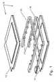
- Fig. 1 is a perspective exploded view of the metalcovers and plastic frame of the package of the present invention;
- Fig. 2 is a detail view of the plastic frame showingthe energy director utilized in the sonic welding process;
- Fig. 3 is an exploded front end view of the metalpackage covers and plastic frame;
- Fig. 4 is side cross-sectional view of a memory cardand package as embodied by the present invention.
- The present invention is a PCMCIA style
peripheraldevice package 10. Referring to Fig. 1, it can be seen thatthepackage 10 comprises chiefly anupper cover 12, alowercover 14, anupper frame element 16, and alower frameelement 18. Thecovers 12 & 14 are formed from stampedmetal, and theframe elements 16 & 18 are molded plastic. - While the material for the covers is chosen to bestamped metal, there is no requirement that it be so. Anyrigid material will suffice. However, if the cover is of aconductive material, it will serve to reduce EMI, RF and ESDproblems, these being factors which electronic devices seekto minimize. It should be further noted that conductivematerial cannot be eliminated completely as PCMCIA requiresa grounding point. The
covers 12 & 14 will generally bemirror images of each other, but may not be in certainapplications. - An optional addition to the present invention is tocoat the interior of the
covers 12 & 14 with a thin layer of a non-conductive material. This allows the finished productto have a conductive exterior with a non-conductiveinterior, thus isolating the conductivity of the interior ofthe package. - Referring now to Figs. 2 & 3, a
lower energy director 20 extends above one-half of the perimeter upper surface ofthelower frame element 18. A corresponding energy directorelement 22 extends along one-half of the lower perimetersurface of theupper frame element 16. Theseenergydirectors 20 & 22 mate with the corresponding frame surfaceto form the weld during the sonic welding process. - A
polarizing key 24 is located at a corner of thelowerframe element 18. Thepolarizing key 24 defines how thePCMCIA style peripheral device mates with the device inwhich it is being used. The polarizing key is defined for agiven use by PCMCIA. - In order to facilitate bonding, the edges of the
covers 12 & 14 are bent to conform generally to the shape of theframe elements 16 & 18. In addition,metal fingers 26 areprovided on each end of thecovers 12 & 14. Themetalfingers 26 curl inward, and are encased in theplastic frameelements 16 & 18 during the molding process. The fingersmay be further secured during the bonding process. The freeends of thefingers 26 may be provided with a non-linershape to cause them to be more securely embedded in theplastic frame elements 16 & 18. In one embodiment, the ends of thefingers 26 have a diamond shape to ensure that onceembedded in the plastic, they cannot be pulled out. - This procedure of embedding the
fingers 26 in theplastic frame elements 16 & 18 ensures that when the twoframe elements are bonded, the two halves of the package aresecurely affixed to each other. Thecovers 12 & 14 beingwrapped around theframe elements 16 & 18 also serves tostrengthen the package due to there being a double layer ofmetal at the perimeter. - The manufacture of the PCMCIA style peripheral devicewith its package is accomplished as follows: first, theupper and
lower covers 12 & 14 are stamped. Thecovers 12 &14 are then mated with theframe elements 16 & 18. This isaccomplished by injection molding. Thecovers 12 & 14 areplaced into a mold, where they are "self-secured" inposition. The self-securing is accomplished by the geometryand dimensions of thecovers 12 & 14. Thecovers 12 & 14are stamped to be slightly wider than the mold. Thus thecovers are slightly sprung when they are placed into themold, and remain in the proper position for the injectionprocess. Certainly there is no requirement that the coversbe self-secured in the mold. Any means of securing willsuffice. - The
plastic frame elements 16 & 18 are then shot intothe mold. As the plastic frames are molded, themetalfingers 26 on thecovers 12 & 14 become embedded in theframe elements 16 & 18 so that separation of thecovers 12 &14 from theframe elements 16 & 18 cannot take place. Theend result of the molding process is that thecovers 12 & 14have a metal surface exposed at their sides to create agrounding point when bonded together. Further toward theinterior of the unit, theplastic energy directors 20 & 22are also exposed to facilitate bonding. - One aspect of using an injection molding process isthat injection molding requires that ejector pins 17 beprovided on the
frame elements 16 & 18. In the presentinvention, the ejector pins 17 are also used to position aPCB 28 that is to be packaged in thepackage 10. Thepins 17 provide a supporting surface for thePCB 28 which can beadjusted to any height desired for a particular application.Thus an element necessary for the injection process becomesa key for the positioning of the board in the package.Positioning of the PCB is therefore accomplished easily andat minimal additional cost. - The
energy directors 20 & 22 are then sonic welded tothe opposing plastic frame element so that theupper frameelement 16 is permanently bonded to thelower frame element 18, both of which encase thePCB 28. - Thus the covers are secured to the frame elements,which in turn are welded to each other. This ensures thatthe memory card package will be very reliable and durable,and that the package height is controlled.
- It should be noted that it is envisioned that thebonding process between the cover elements may also beperformed by resistance welding.
- A further option is to inject a foam into the interiorof the package which would crystallize and act as aninsulator or a heat sink.
- It should also be noted that in practice, a cardmanufacturer will receive the two cover halves ready forwelding, and will be the supplier of the board. Because thepackage has a modular design, it will accommodate manydifferent connectors. Further, because the packagemanufacturer has accomplished a secure bonding of dissimilarmaterials, the metal covers bonded to the plastic frame, thebonding required by the card manufacturer is a simpleprocess involving only bonding of like materials, i.e.plastic to plastic sonic welding.
- The above disclosure is not intended as limiting.Those skilled in the art will readily observe that numerousmodifications and alterations of the device may be madewhile retaining the teachings of the invention.Accordingly, the above disclosure should be construed aslimited only by the metes and bounds of the appended claims.
Claims (6)
- A method of manufacturing a package (10) for a PCB,the method comprising the steps of:a) stamping metal covers (12, 14) to a size marginallylarger than a mold in am injection molding process;b) bending edges of said covers to generally conform toan intended shape of a frame element;c) inserting the covers into a mold in an injectionmolding process where they are slightly sprung and thussecure themselves in position;d) shooting plastic frame elements (16,18) into the moldso that the edges of the covers become embedded in the frameelements;e) removing said covers from said mold;f) positioning the PCB (28) between two covers; andg) bonding the plastic frame elements together so that apackage (10) is formed.
- The method of claim 1 wherein the bonding process issonic welding.
- The method of claim 1 wherein the bonding process isresistance welding.
- The method of claim 1 wherein the bonding processutilizes adhesives.
- The method of claim 1 wherein interior surfaces ofthe covers (12,14) are coated with a thin layer of non-conductivematerial before the PCB (28) is positioned betweenthe two covers.
- The method of claim 1 wherein the edges of the covers(12,14) include projections (26) for anchoring the covers inthe frame element.
Applications Claiming Priority (3)
| Application Number | Priority Date | Filing Date | Title |
|---|---|---|---|
| US08/092,012US5397857A (en) | 1993-07-15 | 1993-07-15 | PCMCIA standard memory card frame |
| US92012 | 1993-07-15 | ||
| EP94921509AEP0682597B1 (en) | 1993-07-15 | 1994-07-13 | Pcmcia standard memory card package |
Related Parent Applications (1)
| Application Number | Title | Priority Date | Filing Date |
|---|---|---|---|
| EP94921509ADivisionEP0682597B1 (en) | 1993-07-15 | 1994-07-13 | Pcmcia standard memory card package |
Publications (3)
| Publication Number | Publication Date |
|---|---|
| EP0967571A2 EP0967571A2 (en) | 1999-12-29 |
| EP0967571A3 EP0967571A3 (en) | 2001-01-17 |
| EP0967571B1true EP0967571B1 (en) | 2003-02-26 |
Family
ID=22230804
Family Applications (4)
| Application Number | Title | Priority Date | Filing Date |
|---|---|---|---|
| EP94921509AExpired - LifetimeEP0682597B1 (en) | 1993-07-15 | 1994-07-13 | Pcmcia standard memory card package |
| EP99118161AExpired - LifetimeEP0967571B1 (en) | 1993-07-15 | 1994-07-13 | PCMCIA standard memory card package |
| EP99118160ARevokedEP0962884B1 (en) | 1993-07-15 | 1994-07-13 | PCMCIA Standard memory card package |
| EP98114528AExpired - LifetimeEP0884163B1 (en) | 1993-07-15 | 1994-07-13 | PCMCIA standard memory card package |
Family Applications Before (1)
| Application Number | Title | Priority Date | Filing Date |
|---|---|---|---|
| EP94921509AExpired - LifetimeEP0682597B1 (en) | 1993-07-15 | 1994-07-13 | Pcmcia standard memory card package |
Family Applications After (2)
| Application Number | Title | Priority Date | Filing Date |
|---|---|---|---|
| EP99118160ARevokedEP0962884B1 (en) | 1993-07-15 | 1994-07-13 | PCMCIA Standard memory card package |
| EP98114528AExpired - LifetimeEP0884163B1 (en) | 1993-07-15 | 1994-07-13 | PCMCIA standard memory card package |
Country Status (8)
| Country | Link |
|---|---|
| US (3) | US5397857A (en) |
| EP (4) | EP0682597B1 (en) |
| JP (1) | JP3059760B2 (en) |
| KR (1) | KR100192074B1 (en) |
| AU (1) | AU677085C (en) |
| CA (1) | CA2143685C (en) |
| DE (4) | DE69432196T2 (en) |
| WO (1) | WO1995002499A1 (en) |
Families Citing this family (97)
| Publication number | Priority date | Publication date | Assignee | Title |
|---|---|---|---|---|
| US5397857A (en)* | 1993-07-15 | 1995-03-14 | Dual Systems | PCMCIA standard memory card frame |
| USD368082S (en) | 1994-05-07 | 1996-03-19 | Sony Corporation | Memory card |
| US5526235A (en)* | 1994-06-23 | 1996-06-11 | Garmin Communication And Navigation | Electronic storage device and receptacle |
| US5502892A (en)* | 1994-07-01 | 1996-04-02 | Maxconn Incorporated | Method of forming a welded encasement for a computer card |
| USD364861S (en) | 1994-09-01 | 1995-12-05 | Franklin Electronic Publishers, Incorporated | Computer card package |
| US5621363A (en)* | 1994-10-03 | 1997-04-15 | Motorola, Inc. | Modem having an electromagnetic shield for a controller |
| US5575670A (en)* | 1995-03-06 | 1996-11-19 | Eaton Corporation | Dust protection for PCMCIA card and socket |
| US5574628A (en)* | 1995-05-17 | 1996-11-12 | The Whitaker Corporation | Rigid PCMCIA frame kit |
| US5510959A (en)* | 1995-05-17 | 1996-04-23 | The Whitaker Corporation | High density PCMCIA frame kit |
| EP0823194A1 (en)* | 1995-05-17 | 1998-02-11 | The Whitaker Corporation | Rigid pcmcia frame kit |
| US5861602A (en)* | 1995-07-24 | 1999-01-19 | International Business Machines Corporation | Snap together PCMCIA cards with laser tack welded seams |
| JP3338976B2 (en)* | 1995-07-27 | 2002-10-28 | モレックス インコーポレーテッド | Connection terminal for electromagnetic shield |
| US5548485A (en)* | 1995-09-29 | 1996-08-20 | Itt Corporation | IC card rigidized cover |
| GB2306789B (en)* | 1995-10-24 | 1999-10-27 | View Technology Co Ltd 3 | PCMCIA Card housing cover |
| DE59710554D1 (en)* | 1996-01-31 | 2003-09-18 | Francotyp Postalia Ag | franking machine |
| US6320252B1 (en)* | 1996-04-05 | 2001-11-20 | Berg Technology, Inc. | Pc |
| US6091605A (en)* | 1996-04-26 | 2000-07-18 | Ramey; Samuel C. | Memory card connector and cover apparatus and method |
| US5894167A (en)* | 1996-05-08 | 1999-04-13 | Micron Technology, Inc. | Encapsulant dam standoff for shell-enclosed die assemblies |
| US5833785A (en)* | 1996-08-12 | 1998-11-10 | Great American Gumball Corporation | Enclosing a small-format electrical device |
| US5892660A (en) | 1996-08-29 | 1999-04-06 | Micron Technology, Inc. | Single in line memory module adapter |
| DE29615553U1 (en)* | 1996-09-06 | 1996-10-31 | Stocko Metallwarenfabriken Henkels Und Sohn Gmbh & Co, 42327 Wuppertal | Housing for personal computer cards (PC cards) |
| US5712766A (en)* | 1996-10-17 | 1998-01-27 | Minnesota Mining And Manufacturing Company | One-piece housing and interlocking connector for IC card assemblies |
| KR100512232B1 (en)* | 1996-11-08 | 2005-09-05 | 에프씨아이 | Electronic card |
| US6144563A (en)* | 1997-06-19 | 2000-11-07 | 3M Innovative Properties Company | Protection card for IC card slot |
| JPH11144450A (en) | 1997-11-10 | 1999-05-28 | Fujitsu Takamisawa Component Ltd | Memory card |
| US6128195A (en)* | 1997-11-18 | 2000-10-03 | Hestia Technologies, Inc. | Transfer molded PCMCIA standard cards |
| DE29722142U1 (en) | 1997-12-16 | 1998-02-12 | Stocko Metallwarenfabriken Henkels & Sohn GmbH & Co, 42327 Wuppertal | Adapter for contacting chip cards |
| US6102715A (en) | 1998-02-10 | 2000-08-15 | The Great American Gumball Corporation | Personal computer peripheral device adapter |
| DE59801853D1 (en)* | 1998-02-20 | 2001-11-29 | Stocko Contact Gmbh & Co Kg | Vertical, short chip card reader |
| AU3078699A (en)* | 1998-03-11 | 1999-09-27 | Ericsson Inc. | Portable telephone accessory for temporary storage of fax and data |
| US6398573B1 (en) | 1998-03-31 | 2002-06-04 | Micron Technology, Inc. | Locking assembly for securing semiconductor device to carrier substrate |
| US6071139A (en) | 1998-03-31 | 2000-06-06 | Micron Technology, Inc. | Locking assembly for securing semiconductor device to carrier substrate |
| EP0966184A1 (en)* | 1998-06-08 | 1999-12-22 | Molex Incorporated | IC card housing and method of manufacture |
| JP2000057297A (en) | 1998-08-04 | 2000-02-25 | Honda Tsushin Kogyo Co Ltd | Frame kit for CF card |
| USD416885S (en)* | 1998-08-05 | 1999-11-23 | Honda Tsushin Kogyo Co., Ltd. | Lower metal cover for compact flash card |
| USD416884S (en)* | 1998-08-05 | 1999-11-23 | Honda Tsushin Kogyo Co., Ltd. | Upper metal cover for compact flash card |
| US6166324A (en)* | 1998-08-06 | 2000-12-26 | Methode Electronics, Inc. | PC card housing with insulative cover and ground feature |
| US6282097B1 (en) | 1998-10-28 | 2001-08-28 | Garmin Corporation | Data card having a retractable handle |
| US6215671B1 (en) | 1998-12-10 | 2001-04-10 | Garmin Corporation | Method and apparatus for connecting circuit boards |
| US6250553B1 (en) | 1998-12-30 | 2001-06-26 | Garmin Corporation | Data card having a retractable handle |
| US6198040B1 (en) | 1999-02-25 | 2001-03-06 | Cisco Technology Inc. | Grounding cover method and apparatus for accessible electronic component |
| US6088231A (en)* | 1999-03-03 | 2000-07-11 | Methode Electronics, Inc. | RF and EMI shield |
| US20070137653A1 (en)* | 2000-03-13 | 2007-06-21 | Wood Thomas J | Ventilation interface for sleep apnea therapy |
| US6231363B1 (en) | 1999-06-28 | 2001-05-15 | Itt Manufacturing Enterprises, Inc. | Low profile interconnection |
| US6313400B1 (en) | 1999-07-13 | 2001-11-06 | Itt Manufacturing Enterprises, Inc. | Data card easily assembled housing |
| US6269537B1 (en)* | 1999-07-28 | 2001-08-07 | Methode Electronics, Inc. | Method of assembling a peripheral device printed circuit board package |
| US8102662B2 (en)* | 2007-07-05 | 2012-01-24 | Super Talent Electronics, Inc. | USB package with bistable sliding mechanism |
| US8625270B2 (en) | 1999-08-04 | 2014-01-07 | Super Talent Technology, Corp. | USB flash drive with deploying and retracting functionalities using retractable cover/cap |
| US7872871B2 (en)* | 2000-01-06 | 2011-01-18 | Super Talent Electronics, Inc. | Molding methods to manufacture single-chip chip-on-board USB device |
| US7830666B2 (en) | 2000-01-06 | 2010-11-09 | Super Talent Electronics, Inc. | Manufacturing process for single-chip MMC/SD flash memory device with molded asymmetric circuit board |
| US8141240B2 (en) | 1999-08-04 | 2012-03-27 | Super Talent Electronics, Inc. | Manufacturing method for micro-SD flash memory card |
| US7466556B2 (en)* | 1999-08-04 | 2008-12-16 | Super Talent Electronics, Inc. | Single chip USB packages with swivel cover |
| US7447037B2 (en) | 1999-08-04 | 2008-11-04 | Super Talent Electronics, Inc. | Single chip USB packages by various assembly methods |
| US7535719B2 (en)* | 1999-08-04 | 2009-05-19 | Super Talent Electronics, Inc. | Single chip USB packages with contact-pins cover |
| DE59905253D1 (en)* | 1999-09-07 | 2003-05-28 | Htp High Tech Plastics Ag Neud | Disc-shaped plastic body with insert |
| USD434771S (en)* | 1999-10-05 | 2000-12-05 | Honda Tsushin Kogyo Co., Ltd. | Upper metal cover for compact flash card |
| USD442964S1 (en) | 1999-10-05 | 2001-05-29 | Honda Tsushin Kogyo Co., Ltd. | Lower metal cover for compact flash card |
| US20080286990A1 (en)* | 2003-12-02 | 2008-11-20 | Super Talent Electronics, Inc. | Direct Package Mold Process For Single Chip SD Flash Cards |
| JP2002094689A (en)* | 2000-06-07 | 2002-03-29 | Sony Computer Entertainment Inc | Program execution system, program execution device, relay device, and recording medium |
| US6337797B1 (en) | 2000-08-10 | 2002-01-08 | Teconn Electronics Inc. | Network interface card frame |
| US6628523B2 (en)* | 2001-02-08 | 2003-09-30 | Denso Corporation | Casing for electronic control unit |
| US6546621B2 (en)* | 2001-03-09 | 2003-04-15 | 3 View Technology Co., Ltd. | Package structure and method for a card |
| DE20201237U1 (en)* | 2002-01-28 | 2002-06-13 | SCM Microsystems GmbH, 85737 Ismaning | Smart card reader |
| DE10210993A1 (en)* | 2002-03-13 | 2003-10-02 | Hubert Stueken Gmbh & Co | Cap for safety fuse with hood-shaped body with bottom and edge sections, has several protrusion on edge section insertable clampingly on object |
| US20040017673A1 (en)* | 2002-07-24 | 2004-01-29 | Chao Michael C. | Peripheral device packages |
| US7326862B2 (en)* | 2003-02-13 | 2008-02-05 | Parker-Hannifin Corporation | Combination metal and plastic EMI shield |
| US7005573B2 (en) | 2003-02-13 | 2006-02-28 | Parker-Hannifin Corporation | Composite EMI shield |
| TW577624U (en)* | 2003-03-14 | 2004-02-21 | View Technology Co Ltd 3 | Package structure of small-sized card |
| US7094633B2 (en) | 2003-06-23 | 2006-08-22 | Sandisk Corporation | Method for efficiently producing removable peripheral cards |
| US7416132B2 (en)* | 2003-07-17 | 2008-08-26 | Sandisk Corporation | Memory card with and without enclosure |
| US20050013106A1 (en)* | 2003-07-17 | 2005-01-20 | Takiar Hem P. | Peripheral card with hidden test pins |
| EP1649410A2 (en)* | 2003-07-17 | 2006-04-26 | SanDisk Corporation | Memory card with raised portion |
| US20050156333A1 (en)* | 2003-09-11 | 2005-07-21 | Super Talent Electronics Inc. | Narrow Universal-Serial-Bus (USB) Flash-Memory Card with Straight Sides using a Ball-Grid-Array (BGA) Chip |
| US7294919B2 (en)* | 2003-11-26 | 2007-11-13 | Avago Technologies General Ip (Singapore) Pte. Ltd. | Device having a complaint element pressed between substrates |
| US7872873B2 (en) | 2003-12-02 | 2011-01-18 | Super Talent Electronics, Inc. | Extended COB-USB with dual-personality contacts |
| US7440286B2 (en)* | 2005-04-21 | 2008-10-21 | Super Talent Electronics, Inc. | Extended USB dual-personality card reader |
| US8998620B2 (en)* | 2003-12-02 | 2015-04-07 | Super Talent Technology, Corp. | Molding method for COB-EUSB devices and metal housing package |
| US8102657B2 (en)* | 2003-12-02 | 2012-01-24 | Super Talent Electronics, Inc. | Single shot molding method for COB USB/EUSB devices with contact pad ribs |
| US7049172B2 (en)* | 2004-02-06 | 2006-05-23 | 3 View Technology Co., Ltd. | Packaging structure and process of electronic card |
| US20080195817A1 (en)* | 2004-07-08 | 2008-08-14 | Super Talent Electronics, Inc. | SD Flash Memory Card Manufacturing Using Rigid-Flex PCB |
| JP4536467B2 (en)* | 2004-09-17 | 2010-09-01 | 株式会社エヌ・ティ・ティ・ドコモ | Flat circuit housing |
| US7607221B2 (en)* | 2004-11-04 | 2009-10-27 | Piranha Plastics | Method of making an electronic device housing |
| US7908080B2 (en) | 2004-12-31 | 2011-03-15 | Google Inc. | Transportation routing |
| DE102006008332B4 (en)* | 2005-07-11 | 2009-06-04 | Fraunhofer-Gesellschaft zur Förderung der angewandten Forschung e.V. | Process for the production of a functional structural unit and functional structural unit |
| US7518880B1 (en) | 2006-02-08 | 2009-04-14 | Bi-Link | Shielding arrangement for electronic device |
| US7928010B2 (en)* | 2006-10-20 | 2011-04-19 | Sandisk Corporation | Method for producing portable memory devices |
| US8013332B2 (en)* | 2006-10-20 | 2011-09-06 | Sandisk Technologies Inc. | Portable memory devices |
| KR100790403B1 (en) | 2007-03-16 | 2008-01-03 | (주)우전 | Expandable card package for personal computer and manufacturing method |
| US8254134B2 (en) | 2007-05-03 | 2012-08-28 | Super Talent Electronics, Inc. | Molded memory card with write protection switch assembly |
| US7789680B2 (en)* | 2007-07-05 | 2010-09-07 | Super Talent Electronics, Inc. | USB device with connected cap |
| US8102658B2 (en)* | 2007-07-05 | 2012-01-24 | Super Talent Electronics, Inc. | Micro-SD to secure digital adaptor card and manufacturing method |
| DE602008006756D1 (en) | 2007-09-24 | 2011-06-16 | Saint Gobain Abrasifs Sa | GRINDING PRODUCTS WITH ACTIVE FILLERS |
| US8491339B2 (en) | 2007-12-28 | 2013-07-23 | Molex Incorporated | Card adapter |
| WO2009086530A1 (en)* | 2007-12-28 | 2009-07-09 | Molex Incorporated | Card adapter |
| US8406001B2 (en)* | 2009-02-27 | 2013-03-26 | Dualsonic, Inc. | Electronic housing, assemblies therefor and methods of making same |
| US20100257732A1 (en)* | 2009-04-14 | 2010-10-14 | Ziberna Frank J | Shielding Arrangement for Electronic Device |
| US9504175B2 (en)* | 2012-12-12 | 2016-11-22 | Fourte Internatinal, Ltd. | Solid-state drive housing, a solid-state disk using the same and an assembling process thereof |
Family Cites Families (67)
| Publication number | Priority date | Publication date | Assignee | Title |
|---|---|---|---|---|
| US35873A (en)* | 1862-07-15 | Improvement in hand tenoning-machines | ||
| US2458327A (en)* | 1943-09-20 | 1949-01-04 | Robert O Wood | Production of molded articles |
| US3297800A (en)* | 1961-04-24 | 1967-01-10 | Macoid Ind Inc | Method of securing a waterstop between concrete panels |
| US3579817A (en)* | 1969-05-21 | 1971-05-25 | Alpha Metals | Cover for coplanar walls of an open top circuit package |
| US3901731A (en)* | 1971-02-15 | 1975-08-26 | Alsthom Cgee | Thin sheet apparatus for supplying and draining liquid |
| US4164068A (en)* | 1977-08-18 | 1979-08-14 | Exxon Research & Engineering Co. | Method of making bipolar carbon-plastic electrode structure-containing multicell electrochemical device |
| US4305897A (en)* | 1978-12-28 | 1981-12-15 | Hitachi Chemical Company, Ltd. | Packaging process for semiconductors |
| DE3019645A1 (en)* | 1980-05-22 | 1981-12-03 | Siemens AG, 1000 Berlin und 8000 München | INSULATED INSERT WITH HIGH STRENGTH RESISTANCE |
| US4399487A (en)* | 1980-09-12 | 1983-08-16 | Siemens Ag | Insulated plug-in module |
| US5013516A (en)* | 1983-05-25 | 1991-05-07 | Showa Denko K.K. | Method of manufacturing container covers |
| JPS61133489A (en)* | 1984-12-03 | 1986-06-20 | Mitsubishi Plastics Ind Ltd | memory card |
| JPH0698865B2 (en)* | 1986-02-21 | 1994-12-07 | 株式会社東芝 | Memory card |
| US4717989A (en)* | 1987-03-30 | 1988-01-05 | Motorola Inc. | Heat sink, EMI shield and controller module assembly for a portable radio transceiver |
| JPS63242694A (en)* | 1987-03-31 | 1988-10-07 | 三菱電機株式会社 | semiconductor device card |
| JPS63281895A (en)* | 1987-05-14 | 1988-11-18 | セイコーエプソン株式会社 | memory card |
| JPS645894A (en)* | 1987-06-29 | 1989-01-10 | Toshiba Corp | Thin-type mounting type semiconductor device |
| JPS6440395A (en)* | 1987-08-05 | 1989-02-10 | Fanuc Ltd | Ic card |
| US4811165A (en)* | 1987-12-07 | 1989-03-07 | Motorola, Inc. | Assembly for circuit modules |
| FR2625840B1 (en)* | 1988-01-13 | 1990-06-29 | Sgs Thomson Microelectronics | HOUSING FOR CONTAINING A FRAGILE ELEMENT SUCH AS A LOGIC CIRCUIT AND METHOD FOR ASSEMBLING SUCH A HOUSING |
| JPH0818474B2 (en)* | 1988-02-02 | 1996-02-28 | 日本電気株式会社 | Information card |
| JPH01299091A (en)* | 1988-05-26 | 1989-12-01 | Nec Corp | Memory card |
| JPH0818475B2 (en)* | 1988-07-01 | 1996-02-28 | 三菱電機株式会社 | IC card |
| JPH0218097A (en)* | 1988-07-06 | 1990-01-22 | Mitsubishi Electric Corp | semiconductor device card |
| JPH0245195A (en)* | 1988-08-06 | 1990-02-15 | Seiko Epson Corp | Connection of frame ground |
| JPH0749235B2 (en)* | 1988-10-28 | 1995-05-31 | 日本電気株式会社 | Memory card |
| JPH0634152Y2 (en)* | 1988-12-08 | 1994-09-07 | Multifunction card | |
| JPH02164599A (en)* | 1988-12-19 | 1990-06-25 | Toshiba Corp | Thin electronic machinery |
| JPH02270597A (en)* | 1989-04-11 | 1990-11-05 | Mitsubishi Electric Corp | Ic card |
| JP2612339B2 (en)* | 1989-04-18 | 1997-05-21 | 三菱電機株式会社 | Electronic equipment housing |
| US5084802A (en)* | 1989-05-16 | 1992-01-28 | At&T Bell Laboratories | Method for manufacture of EMI reducing circuit card apparatus |
| JP2559849B2 (en)* | 1989-05-23 | 1996-12-04 | 三菱電機株式会社 | IC card |
| JPH0327598A (en)* | 1989-06-23 | 1991-02-05 | Toshiba Corp | Thin electronic device and its manufacturing method |
| JPH0326598A (en)* | 1989-06-23 | 1991-02-05 | Toshiba Corp | Electronic circuit unit |
| JP2552730B2 (en)* | 1989-06-26 | 1996-11-13 | 住友金属工業株式会社 | Metal case for IC storage |
| US5014160A (en)* | 1989-07-05 | 1991-05-07 | Digital Equipment Corporation | EMI/RFI shielding method and apparatus |
| JPH07121635B2 (en)* | 1989-09-09 | 1995-12-25 | 三菱電機株式会社 | IC card |
| US5107404A (en)* | 1989-09-14 | 1992-04-21 | Astec International Ltd. | Circuit board assembly for a cellular telephone system or the like |
| JPH0648774Y2 (en)* | 1989-09-21 | 1994-12-12 | 沖電気工業株式会社 | Card type integrated circuit and connector terminal structure |
| US5124888A (en)* | 1990-01-25 | 1992-06-23 | Tokyo Electric Co., Ltd. | Electric circuit apparatus |
| US5148350A (en)* | 1990-04-23 | 1992-09-15 | Motorola, Inc. | Portable electronics apparatus housing and chassis |
| JPH04153096A (en)* | 1990-10-18 | 1992-05-26 | Mitsubishi Electric Corp | portable storage device |
| US5206796A (en)* | 1991-03-11 | 1993-04-27 | John Fluke Mfg. Co. Inc. | Electronic instrument with emi/esd shielding system |
| US5208732A (en)* | 1991-05-29 | 1993-05-04 | Texas Instruments, Incorporated | Memory card with flexible conductor between substrate and metal cover |
| US5544007A (en)* | 1991-07-19 | 1996-08-06 | Kabushiiki Kaisha Toshiba | Card-shaped electronic device used with an electronic apparatus and having shield plate with conductive portion on a lateral side |
| DE69227690T2 (en)* | 1991-08-09 | 1999-05-20 | Tandem Computers Inc., Cupertino, Calif. | ELECTRONIC ASSEMBLY WITH IMPROVED EARTHING |
| JPH0550691A (en)* | 1991-08-21 | 1993-03-02 | Seiko Epson Corp | Carriage control device |
| DE4129238A1 (en)* | 1991-09-03 | 1993-03-04 | Bosch Gmbh Robert | ELECTRICAL DEVICE, ESPECIALLY SWITCHING AND CONTROL UNIT FOR MOTOR VEHICLES |
| US5383098A (en)* | 1991-09-19 | 1995-01-17 | Motorola, Inc. | Shield assembly |
| FR2681711B1 (en)* | 1991-09-20 | 1996-08-02 | Itt Composants Instr | PORTABLE CASE FOR AN ELECTRONIC MEMORY CARD |
| EP0536560B1 (en)* | 1991-10-11 | 1996-06-12 | Asea Brown Boveri Ag | In- and/or output device for process data |
| US5414253A (en)* | 1991-12-03 | 1995-05-09 | Texas Instruments Incorporated | Integrated circuit card |
| CA2057518C (en)* | 1991-12-09 | 1996-11-19 | Albert John Kerklaan | Jacketted circuit card |
| CA2084496C (en)* | 1992-02-12 | 1998-11-03 | William F. Weber | Emi internal shield apparatus and methods |
| US5242310A (en)* | 1992-06-19 | 1993-09-07 | Data Trek Corporation | PC I/O card |
| US5333100A (en)* | 1992-06-29 | 1994-07-26 | Itt Corporation | Data card perimeter shield |
| US5252782A (en)* | 1992-06-29 | 1993-10-12 | E-Systems, Inc. | Apparatus for providing RFI/EMI isolation between adjacent circuit areas on a single circuit board |
| US5308251A (en)* | 1992-08-10 | 1994-05-03 | The Whitaker Corporation | Mounting bracket with ESD protection for an electrical connector |
| US5330360A (en)* | 1992-08-21 | 1994-07-19 | The Whitaker Corporation | Memory card and connector therefor |
| US5339222A (en) | 1993-04-06 | 1994-08-16 | The Whitaker Corporation | Shielded printed circuit card holder |
| US5476387A (en)* | 1993-06-07 | 1995-12-19 | Methode Electronics Inc. | Memory card frame and cover kit |
| US5397857A (en)* | 1993-07-15 | 1995-03-14 | Dual Systems | PCMCIA standard memory card frame |
| US5391083A (en)* | 1994-02-25 | 1995-02-21 | R. A. Tool & Die, Inc. | Computer card connector |
| US5490043A (en)* | 1994-04-15 | 1996-02-06 | Hon Hai Precision Ind. Co., Ltd. | Grounding clip structure of I/O card |
| US5470237A (en)* | 1994-06-20 | 1995-11-28 | Elco Corporation | Latch mechanism for joining the cover and connector of a removable memory device |
| US5502892A (en)* | 1994-07-01 | 1996-04-02 | Maxconn Incorporated | Method of forming a welded encasement for a computer card |
| US5475919B1 (en)* | 1994-10-07 | 2000-10-17 | Three View Technology Co Ltd | Pcmcia card manufacturing process |
| US5510959A (en)* | 1995-05-17 | 1996-04-23 | The Whitaker Corporation | High density PCMCIA frame kit |
- 1993
- 1993-07-15USUS08/092,012patent/US5397857A/ennot_activeExpired - Lifetime
- 1994
- 1994-07-13EPEP94921509Apatent/EP0682597B1/ennot_activeExpired - Lifetime
- 1994-07-13DEDE69432196Tpatent/DE69432196T2/ennot_activeExpired - Fee Related
- 1994-07-13EPEP99118161Apatent/EP0967571B1/ennot_activeExpired - Lifetime
- 1994-07-13AUAU72211/94Apatent/AU677085C/ennot_activeCeased
- 1994-07-13WOPCT/US1994/007903patent/WO1995002499A1/enactiveIP Right Grant
- 1994-07-13EPEP99118160Apatent/EP0962884B1/ennot_activeRevoked
- 1994-07-13DEDE69432324Tpatent/DE69432324T2/ennot_activeExpired - Fee Related
- 1994-07-13DEDE69424324Tpatent/DE69424324T2/ennot_activeExpired - Fee Related
- 1994-07-13CACA002143685Apatent/CA2143685C/ennot_activeExpired - Fee Related
- 1994-07-13KRKR1019950700878Apatent/KR100192074B1/ennot_activeCeased
- 1994-07-13JPJP7504714Apatent/JP3059760B2/ennot_activeExpired - Fee Related
- 1994-07-13DEDE69423960Tpatent/DE69423960T2/ennot_activeExpired - Fee Related
- 1994-07-13EPEP98114528Apatent/EP0884163B1/ennot_activeExpired - Lifetime
- 1994-12-01USUS08/348,535patent/US5490891A/ennot_activeCeased
- 1998
- 1998-02-13USUS09/023,780patent/USRE36540E/ennot_activeExpired - Lifetime
Also Published As
| Publication number | Publication date |
|---|---|
| KR100192074B1 (en) | 1999-06-15 |
| EP0962884B1 (en) | 2003-03-19 |
| DE69423960D1 (en) | 2000-05-18 |
| DE69432196D1 (en) | 2003-04-03 |
| JP3059760B2 (en) | 2000-07-04 |
| EP0682597A4 (en) | 1997-12-17 |
| DE69424324T2 (en) | 2000-09-14 |
| EP0962884A2 (en) | 1999-12-08 |
| DE69432196T2 (en) | 2003-10-09 |
| EP0682597B1 (en) | 2000-04-12 |
| DE69424324D1 (en) | 2000-06-08 |
| JPH08505727A (en) | 1996-06-18 |
| DE69423960T2 (en) | 2000-08-17 |
| EP0884163B1 (en) | 2000-05-03 |
| EP0962884A3 (en) | 2001-01-17 |
| DE69432324D1 (en) | 2003-04-24 |
| AU677085C (en) | 2006-08-17 |
| USRE36540E (en) | 2000-02-01 |
| EP0967571A2 (en) | 1999-12-29 |
| KR950702904A (en) | 1995-08-23 |
| US5397857A (en) | 1995-03-14 |
| AU677085B2 (en) | 1997-04-10 |
| CA2143685F (en) | 1995-01-26 |
| AU7221194A (en) | 1995-02-13 |
| EP0884163A1 (en) | 1998-12-16 |
| CA2143685A1 (en) | 1995-01-26 |
| DE69432324T2 (en) | 2004-02-12 |
| WO1995002499A1 (en) | 1995-01-26 |
| EP0682597A1 (en) | 1995-11-22 |
| US5490891A (en) | 1996-02-13 |
| CA2143685C (en) | 2001-12-11 |
| EP0967571A3 (en) | 2001-01-17 |
Similar Documents
| Publication | Publication Date | Title |
|---|---|---|
| EP0967571B1 (en) | PCMCIA standard memory card package | |
| US5563769A (en) | Tabbed cover attach for PCMCIA card packaging and method for attaching the PCMCIA covers to the printed circuit board assembly | |
| US5964595A (en) | Enclosing a small-format electrical device | |
| US5502892A (en) | Method of forming a welded encasement for a computer card | |
| US6381143B1 (en) | Card-typed electronic apparatus having a flat card case housing a plurality of electronic parts | |
| JP3185054B2 (en) | IC card housing and method of manufacturing the same | |
| US6128195A (en) | Transfer molded PCMCIA standard cards | |
| US7030316B2 (en) | Insert molding electronic devices | |
| WO2003096446A1 (en) | Thin battery | |
| JPH09240179A (en) | Ic card and manufacture of ic card and ic card base | |
| US20030043551A1 (en) | Method and circuit module package for automated switch actuator insertion | |
| CN210381002U (en) | Waterproof device of mobile terminal card support and mobile terminal | |
| US20040017673A1 (en) | Peripheral device packages | |
| JPH068681A (en) | Ic card and production thereof | |
| TWM243739U (en) | MMC memory card using TSOP | |
| JPH0818266A (en) | Electromagnetic wave shielding type circuit unit | |
| JPH07276867A (en) | Memory device and manufacturing method thereof | |
| JP2004102338A (en) | Case for electronic device, and its manufacturing method | |
| JPH01275195A (en) | Ic card |
Legal Events
| Date | Code | Title | Description |
|---|---|---|---|
| PUAI | Public reference made under article 153(3) epc to a published international application that has entered the european phase | Free format text:ORIGINAL CODE: 0009012 | |
| 17P | Request for examination filed | Effective date:19990913 | |
| AC | Divisional application: reference to earlier application | Ref document number:682597 Country of ref document:EP | |
| AK | Designated contracting states | Kind code of ref document:A2 Designated state(s):DE FR GB IT NL | |
| AX | Request for extension of the european patent | Free format text:LT;SI | |
| PUAL | Search report despatched | Free format text:ORIGINAL CODE: 0009013 | |
| AK | Designated contracting states | Kind code of ref document:A3 Designated state(s):AT BE CH DE DK ES FR GB GR IE IT LI LU MC NL PT SE | |
| AX | Request for extension of the european patent | Free format text:LT;SI | |
| RIC1 | Information provided on ipc code assigned before grant | Free format text:7G 06K 19/077 A | |
| AKX | Designation fees paid | Free format text:DE FR GB IT NL | |
| 17Q | First examination report despatched | Effective date:20010921 | |
| GRAH | Despatch of communication of intention to grant a patent | Free format text:ORIGINAL CODE: EPIDOS IGRA | |
| GRAH | Despatch of communication of intention to grant a patent | Free format text:ORIGINAL CODE: EPIDOS IGRA | |
| GRAA | (expected) grant | Free format text:ORIGINAL CODE: 0009210 | |
| AC | Divisional application: reference to earlier application | Ref document number:0682597 Country of ref document:EP Kind code of ref document:P | |
| AK | Designated contracting states | Designated state(s):DE FR GB IT NL | |
| REG | Reference to a national code | Ref country code:GB Ref legal event code:FG4D | |
| REF | Corresponds to: | Ref document number:69432196 Country of ref document:DE Date of ref document:20030403 Kind code of ref document:P | |
| ET | Fr: translation filed | ||
| PLBE | No opposition filed within time limit | Free format text:ORIGINAL CODE: 0009261 | |
| STAA | Information on the status of an ep patent application or granted ep patent | Free format text:STATUS: NO OPPOSITION FILED WITHIN TIME LIMIT | |
| 26N | No opposition filed | Effective date:20031127 | |
| PGFP | Annual fee paid to national office [announced via postgrant information from national office to epo] | Ref country code:DE Payment date:20080731 Year of fee payment:15 | |
| PGFP | Annual fee paid to national office [announced via postgrant information from national office to epo] | Ref country code:NL Payment date:20080715 Year of fee payment:15 Ref country code:IT Payment date:20080729 Year of fee payment:15 Ref country code:FR Payment date:20080722 Year of fee payment:15 | |
| PGFP | Annual fee paid to national office [announced via postgrant information from national office to epo] | Ref country code:GB Payment date:20080708 Year of fee payment:15 | |
| GBPC | Gb: european patent ceased through non-payment of renewal fee | Effective date:20090713 | |
| NLV4 | Nl: lapsed or anulled due to non-payment of the annual fee | Effective date:20100201 | |
| REG | Reference to a national code | Ref country code:FR Ref legal event code:ST Effective date:20100331 | |
| PG25 | Lapsed in a contracting state [announced via postgrant information from national office to epo] | Ref country code:FR Free format text:LAPSE BECAUSE OF NON-PAYMENT OF DUE FEES Effective date:20090731 | |
| PG25 | Lapsed in a contracting state [announced via postgrant information from national office to epo] | Ref country code:GB Free format text:LAPSE BECAUSE OF NON-PAYMENT OF DUE FEES Effective date:20090713 | |
| PG25 | Lapsed in a contracting state [announced via postgrant information from national office to epo] | Ref country code:DE Free format text:LAPSE BECAUSE OF NON-PAYMENT OF DUE FEES Effective date:20100202 | |
| PG25 | Lapsed in a contracting state [announced via postgrant information from national office to epo] | Ref country code:IT Free format text:LAPSE BECAUSE OF NON-PAYMENT OF DUE FEES Effective date:20090713 | |
| PG25 | Lapsed in a contracting state [announced via postgrant information from national office to epo] | Ref country code:NL Free format text:LAPSE BECAUSE OF NON-PAYMENT OF DUE FEES Effective date:20100201 |