EP0961285A1 - Device and method for reading nonvolatile memory cells - Google Patents
Device and method for reading nonvolatile memory cellsDownload PDFInfo
- Publication number
- EP0961285A1 EP0961285A1EP98830333AEP98830333AEP0961285A1EP 0961285 A1EP0961285 A1EP 0961285A1EP 98830333 AEP98830333 AEP 98830333AEP 98830333 AEP98830333 AEP 98830333AEP 0961285 A1EP0961285 A1EP 0961285A1
- Authority
- EP
- European Patent Office
- Prior art keywords
- branch
- transistor
- input
- comparator circuit
- memory cells
- Prior art date
- Legal status (The legal status is an assumption and is not a legal conclusion. Google has not performed a legal analysis and makes no representation as to the accuracy of the status listed.)
- Granted
Links
- 230000015654memoryEffects0.000titleclaimsabstractdescription35
- 238000000034methodMethods0.000titleclaimsabstractdescription7
- 230000002596correlated effectEffects0.000claimsabstract3
- 238000001514detection methodMethods0.000claimsdescription3
- 230000000295complement effectEffects0.000claims1
- 238000010586diagramMethods0.000description4
- 238000004088simulationMethods0.000description3
- 230000008030eliminationEffects0.000description2
- 238000003379elimination reactionMethods0.000description2
- 230000004048modificationEffects0.000description2
- 238000012986modificationMethods0.000description2
- 239000000758substrateSubstances0.000description2
- 238000006243chemical reactionMethods0.000description1
- 230000001351cycling effectEffects0.000description1
- 239000006185dispersionSubstances0.000description1
- 230000009977dual effectEffects0.000description1
- 230000000694effectsEffects0.000description1
- 239000000463materialSubstances0.000description1
- 230000004044responseEffects0.000description1
- 239000004065semiconductorSubstances0.000description1
- 230000007704transitionEffects0.000description1
Images


Classifications
- G—PHYSICS
- G11—INFORMATION STORAGE
- G11C—STATIC STORES
- G11C16/00—Erasable programmable read-only memories
- G11C16/02—Erasable programmable read-only memories electrically programmable
- G11C16/06—Auxiliary circuits, e.g. for writing into memory
- G11C16/26—Sensing or reading circuits; Data output circuits
- G11C16/28—Sensing or reading circuits; Data output circuits using differential sensing or reference cells, e.g. dummy cells
- G—PHYSICS
- G11—INFORMATION STORAGE
- G11C—STATIC STORES
- G11C7/00—Arrangements for writing information into, or reading information out from, a digital store
- G11C7/06—Sense amplifiers; Associated circuits, e.g. timing or triggering circuits
- G—PHYSICS
- G11—INFORMATION STORAGE
- G11C—STATIC STORES
- G11C7/00—Arrangements for writing information into, or reading information out from, a digital store
- G11C7/06—Sense amplifiers; Associated circuits, e.g. timing or triggering circuits
- G11C7/062—Differential amplifiers of non-latching type, e.g. comparators, long-tailed pairs
Definitions
- the present inventionrelates to a device and a method for reading nonvolatile memory cells.
- memory cellsare presently read by converting the current flowing into the cell, which is suitably biased, into a voltage, and comparing the voltage thus obtained with a reference voltage generated from a reference cell, the charge state of which is previously known, and is typically a virgin cell.
- the read memory cellconducts a different current according to the stored charge condition, and comparison (carried out by a sense amplifier) with the current flowing in the reference cell allows detecting whether the cell is written or erased, and thus whether the stored datum is a "0" or a "1".
- FIG. 1shows a simplified diagram of a reading device (sense amplifier) 1 connected to an array cell 2 to be read, and to a reference cell 3.
- Sense amplifier 1comprises a circuit 4 preventing phenomena of soft-writing (spurious writing of the cell), a current-voltage converter 5 and a comparator 6.
- reference cellsare formed inside the memory array, using a column of the array as a reference, one for each output. This solution has some advantages, such as low dispersion of the threshold values of the reference cells compared with the values of the memory cells; simplicity of timing, since the reference cells are biased together with the memory cells; and balance of the branches of the sense amplifier.
- a feature which is essential to obtain correct reading of the memory cellsconcerns positioning of the characteristic of the reference cell (reference characteristic), compared with the characteristics of written and erased memory cells, taking into account their distribution.
- the position of the reference characteristicmust be intermediate between the characteristic of the worst erased array cell (curve I E , with threshold Vtc) and the characteristic of the worst programmed cell (curve I W , with threshold Vts).
- known I/V convertersare structured according to two solutions, i.e. unbalance converter, which provides the reference characteristic R 1 of figure 2, and semi-parallel converter which provides the reference characteristic R 2 of figure 3.
- the two solutionshave different fields of application; the first, of figure 2, is suitable for memories operating at high supply levels (5V); the second, of figure 3, is suitable for memories operating at a low voltage (less than 3V).
- the main problemsare derived from the need to correctly position the reference, and to select accurately the gain of the trans-characteristic of the cell (gain seen externally), by modifying loads of the I/V converter 5.
- these operationsare very delicate and costly as to time; in addition, the reference cell (or plurality of reference cells) is not representative of the entire distribution of the array cells, and thus gives rise to a response distribution by the sense amplifier.
- the reference cellsdo not age like the array cells because they are subject to different stresses, they do not undergo the same program/erase cycles as the array cells, and on the other hand they are biased substantially continually during reading.
- the object of the inventionis thus to overcome the above described disadvantages.
- a device and a method for reading nonvolatile memory cellsare provided, as defined respectively in claim 1 and claim 11.
- the reading devicedoes not use particular reference cells, having a previously known charge state, but compares with each other two bits read simultaneously, and preferably two bits of a single byte, using them as a dynamic reference for each other.
- the reading deviceindicated generally at 10, has a first and a second input node 11, 12, connected respectively to a memory cell F1 and F2, and a first and a second output node 13, 14 providing respectively output voltages 01 and 02.
- Cells F1, F2, of nonvolatile type, and in particular of flash typeare preferably cells of a single byte that are read simultaneously, and are biased at their gate terminals by reading voltages V R , which, if the supply voltage has a sufficient value, has the same value as supply voltage Vcc, and otherwise is a boosted supply voltage by an appropriate circuit, in a per se known manner, not discussed in detail.
- Each input node 11, 12is connected by a respective fedback cascode circuit 17, 18, to an input node 19a, 20a of a respective first current mirror circuit 19, 20.
- Fedback cascode circuits 17, 18comprise each an NMOS transistor 21, arranged respectively between nodes 11, 19a, and 12, 20a, and an inverter 22 arranged respectively between nodes 11, 12 and the gate terminal of respective NMOS transistor 21.
- Fedback cascode circuits 17, 18regulate the voltage present on input node 11, 12, so as to prevent soft-writing phenomena, in a known manner.
- First current mirror circuits 19, 20comprise a PMOS transistor 23, diode-connected between nodes 19a, respectively 20a and a supply line 30 set to Vcc, and a transistor 24 connected between supply line 30 and a respective output node 19b, 20b.
- Transistors 23 and 24have gate terminals connected to each other.
- Output nodes 19b, 20bare connected by respective fedback cascode circuits 31, 32, equal to fedback cascade circuits 17, 18, to input nodes 33a, 34a of respective second current mirror circuits 33, 34 of NMOS type, comprising native transistors 35, 36, and thus have a threshold voltage that is lower than that normally provided.
- transistor 35is diode-connected between the respective input node 33a, 34a and ground 38; transistor 36 has a source terminal connected to ground 38 and a drain terminal forming the respective output nodes 33b, 34b.
- Output nodes 33b, 34bare connected by respective fedback cascode circuits 39, 40 respectively to a first and a second input/output node 41a, 41b of a current/voltage converter circuit 41.
- Fedback cascode circuits 39, 40are similar to fedback cascode circuits 17, 18, except the fact that inverter 22 is replaced by a NOR gate 42, having a first input connected to node 33b, respectively 34b, and an other input receiving an enable signal EN supplied from the exterior.
- the output of NOR gate 42is connected to a gate terminal of an NMOS transistor 43 arranged between node 33b, respectively 34b, and nodes 41a, respectively 41b.
- a first equalisation transistor 44 of NMOS typeis connected between nodes 33b and 34b, and has a control terminal receiving a signal ATD.
- a second equalisation transistor 45 of native NMOS typeis connected between gate terminals of NMOS transistors 43, and has a control terminal receiving signal ATD.
- a third equalisation transistor 46is connected between the input/output nodes 41a, 41b of current/voltage converter 41, and has a control terminal receiving signal ATD.
- Equalisation transistors 44-46operate in known manner to equalise to each other the voltages present on nodes 33b, 34b, and the voltages present on nodes 41a, 41b in the equalisation step, when signal ATD (generated on detection of an address transition in the memory comprising the present reading device) has a high value, and are switched off during an actual reading step, such as to allow independent evolution of the two device branches, connected respectively to cell F1 and cell F2, and lead to input/output nodes 41a, 41b, depending on whether cells F1, F2 are written or erased.
- Current/voltage converter 41comprises a pair of load transistors 49, 50 of native NMOS type, diode-connected, and have a source terminal connected to the input node 41a, respectively 41b, a drain terminal connected to supply line 30, a gate terminal connected to the drain terminal, and bulk connected to the source terminal.
- Load transistors 49, 50are of triple-well type, as shown in the cross-section of figure 5, wherein the bulk of load transistors 49, 50 is shown as comprising a P well 100 accommodating a source region 101 and a drain region 102 of N + -type.
- P well 100is electrically connected to source region 101, and is accommodated in an N well 105 biased to Vcc, and in turn is formed in substrate 106, which is grounded.
- the bulkis electrically separated from substrate 106, and has the same potential as source region 101; consequently load transistors 49, 50 have a particularly low threshold voltage, which is not affected by the body effect (according to which the threshold voltage increases when the voltage drop between the body and source regions increases).
- a respective bias branch 51, 52is arranged in parallel with each of the load transistors 49, 50; bias branches 51, 52 are equal to each other, and comprise a PMOS transistor 53 and a native-type NMOS transistor 54; PMOS transistor 53 has a source terminal connected to supply line 30, a gate terminal connected to ground 38, and a drain terminal connected to the drain terminal of NMOS transistor 54; NMOS transistor 54 has a gate terminal receiving signal ATD and a source terminal connected to the respective input/output nodes 41a, 41b.
- bias branches 51, 52initially set the flowing current, in a known manner, and maintain input/output nodes 41a, 41b at voltage Vcc, less the threshold voltage of a native transistor.
- First and second input/output nodes 41a, 41b of current/voltage converter 41are connected to a comparison circuit 58 comprising a first and a second branch 59, 60 which are equal to each other and are arranged in parallel with each other.
- first branch 59comprises a PMOS transistor 63 and three NMOS transistors 65, 67, 69 connected in series between supply line 30 and ground 38;
- second branch 60comprises a PMOS transistor 64 and three NMOS transistors 66, 68, 70, also connected in series between supply line 30 and ground 38.
- NMOS transistors 65-68are of native, low-threshold type; PMOS transistor 63 and NMOS transistors 67, 69 of first branch 59 all have a gate terminal connected to the first input/output node 41a; PMOS transistor 64 and NMOS transistors 68, 70 of second branch 60 all have a gate terminal connected to the second input/output node 41b.
- NMOS transistors 65 and 66 of first and second branch 59, 60are diode-connected, have bulk connected to the respective source terminal, and are also of triple-well type, as load transistors 49, 50.
- PMOS transistors 63, 64 of first and second branch 59, 60have a source terminal connected to supply line 30 and a gate terminal connected to the drain terminal of NMOS transistors 65, 66; the intermediate node between the respective NMOS transistors 65, 67 and 66, 68, forms the first output 13 and, respectively the second output 14 of reading device 10; the source terminal of NMOS transistors 69, 70 is connected to ground 38.
- the circuit of figure 4operates as follows.
- PMOS transistors 63, 64set both outputs 13, 14 to a voltage having the same value as supply voltage Vcc, less the threshold voltage of native NMOS transistors 65, 66 and thus voltages 01 and 02 are both high, corresponding to a logic condition "11" (two-bit logic signal).
- Vais the voltage present at the first input/output node 41a
- Vbis the voltage present at the second input/output node 41b
- the other voltageshave the meaning already explained.
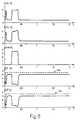
- the cellsdo not absorb current, or absorb small currents, which may be also different from each other.
- the current absorbed by cells F1, F2, and mirrored in the first and second current mirror circuits 19, 20 and 33, 34is not sufficient to lower the voltage at input/output nodes 41a, 41b, which in fact in ideal conditions goes to its maximum value, equal to supply voltage Vcc less the threshold voltage of native load transistors 49, 50 (0.5 V). Consequently PMOS transistors 63, 64 of comparison circuit 58 remain switched off, and NMOS transistors 67-70 remain switched on. Voltages 01 and 02 at outputs 13, 14 are thus low, corresponding to a logic condition "00". This situation corresponds to the simulation of figure 7.
- Voltages 01 and 02are subsequently advantageously buffered by a structure setting their value to a fully CMOS value.
- Elimination of the reference cellsolves the above described problems of criticality, and difficulty of design and control; in addition it allows elimination of all the circuitry necessary for controlling and positioning the memory cell or cells in the EWS (Electrical Wafer Sort) step. Furthermore, it permits time saving in the EWS step, and, for reading an entire byte, requires the use of only four circuits as that described.
Landscapes
- Read Only Memory (AREA)
Abstract
Description
- figure 1 shows the circuit diagram of a sense amplifierof known type;
- figures 2 and 3 show the characteristics of memory cellsand reference cells in two known current/voltage conversionsolutions;
- figure 4 shows a simplified circuit diagram of thereading device according to the invention;
- figure 5 shows a cross-section through a portion of asemiconductor material wafer accommodating a component of thediagram of figure 4; and
- figures 6-8 show plots of electrical quantities measuredon the circuit of figure 4, in three different readingconditions.
Claims (11)
- A device (10) for reading nonvolatile memory cells (F1,F2), having two input nodes (11, 12) connectable to arespective one of two memory cells (F1, F2) storing unknowncharge conditions, characterised by a two-input comparatorcircuit (58), said two-input comparator circuit having twoinputs (41a, 41b), each connected to a respective one of saidtwo input nodes (11, 12), comparing with each other saidcharge conditions, and generating at an output a two-bitsignal (01, 02) coding said charge conditions.
- A device according to claim 1, characterised in thatsaid two-input comparator circuit (58) comprises a first anda second branch (59, 60) equal to each other, and connectedin parallel between a first and a second reference potentialstructure (30, 38); said first branch (59) defining a firstone (41a) of said two inputs and said second branch (60)defining a second one (41b) of said two inputs of said tow-inputcomparator circuit.
- A device according to claim 2, characterised in thatsaid first and second branch (59, 60) comprise each a first(63, 64) and a second (69, 70) transistor connected in seriesto each other, and of complementary type, said first andsecond transistor of each branch having gate terminalsconnected together and to a respective one of said first andsecond inputs (41a, 41b) of said two-input comparator circuit(58).
- A device according to claim 3, characterised in thateach branch (59, 60) of said two-input comparator circuit(58) additionally comprises a third (65, 66) and a fourth(67, 68) transistor connected in series between said first(63, 64) and second transistors (69, 70); said third andfourth transistors being of low-threshold type, and definingbetween each other an intermediate node (13, 14) forming a respective output of said two-input comparator circuit (58).
- A device according to claim 4, characterised in thatsaid first reference potential structure (30) is connected toa supply voltage (Vcc), in that said first transistor (63,64) of said first and second branches (59, 60) is connectedto said first reference potential structure (30), said thirdtransistor (65, 66) of said first and second branches (59,60) is diode-connected between said respective firsttransistor and a respective output (13, 14) of said two-inputcomparator circuit (58), and is of triple-well type.
- A device according to any one of the preceding claims,characterised by charge detection means (17-54) arrangedbetween said two input nodes (11, 12) and said two inputs(41a, 41b) of said two-input comparator circuit (58), andgenerates electrical quantities correlated to said chargeconditions.
- A device according to claim 6, characterised in thatsaid charge detection means comprises a current/voltageconverter (41).
- A device according to claim 6 or 7, characterised inthat said current/voltage converter (41) comprises twobranches, each branch including at least one load transistor(49, 50) connected between a respective input node (11, 12)and a supply line (30); said load transistors being diode-connectedand being of triple-well type.
- A device according to claim 8, characterised in thateach branch of said current/voltage converter (41)additionally comprises a first (19, 20) and a second (33, 34)current mirror circuit arranged between a respective inputnode (11, 12) and a respective load transistor (49, 50).
- A device according to claim 9, characterised in that said current mirror circuits (33, 34) are connected to saidrespective load transistors (49, 50) and are of low thresholdtype.
- A method for reading nonvolatile memory cells,comprising the steps of:simultaneously supplying two memory cells (F1, F2), bothmemory cells storing a respective unknown charge condition;generating two electrical quantities (Va, Vb), saidelectrical quantities being correlated to a respective one ofsaid charge conditions;
characterised by the steps of:comparing said two electrical quantities (Va, Vb) with eachother;generating a two-bit signal (01, 02) according to saidcomparison.
Priority Applications (4)
| Application Number | Priority Date | Filing Date | Title |
|---|---|---|---|
| DE69820594TDE69820594D1 (en) | 1998-05-29 | 1998-05-29 | Arrangement and method for reading non-volatile memory cells |
| EP98830333AEP0961285B1 (en) | 1998-05-29 | 1998-05-29 | Device and method for reading nonvolatile memory cells |
| US09/322,460US6181602B1 (en) | 1998-05-29 | 1999-05-28 | Device and method for reading nonvolatile memory cells |
| JP15223299AJP4237337B2 (en) | 1998-05-29 | 1999-05-31 | Apparatus and method for reading non-volatile memory cells |
Applications Claiming Priority (1)
| Application Number | Priority Date | Filing Date | Title |
|---|---|---|---|
| EP98830333AEP0961285B1 (en) | 1998-05-29 | 1998-05-29 | Device and method for reading nonvolatile memory cells |
Publications (2)
| Publication Number | Publication Date |
|---|---|
| EP0961285A1true EP0961285A1 (en) | 1999-12-01 |
| EP0961285B1 EP0961285B1 (en) | 2003-12-17 |
Family
ID=8236669
Family Applications (1)
| Application Number | Title | Priority Date | Filing Date |
|---|---|---|---|
| EP98830333AExpired - LifetimeEP0961285B1 (en) | 1998-05-29 | 1998-05-29 | Device and method for reading nonvolatile memory cells |
Country Status (4)
| Country | Link |
|---|---|
| US (1) | US6181602B1 (en) |
| EP (1) | EP0961285B1 (en) |
| JP (1) | JP4237337B2 (en) |
| DE (1) | DE69820594D1 (en) |
Cited By (3)
| Publication number | Priority date | Publication date | Assignee | Title |
|---|---|---|---|---|
| US6538922B1 (en) | 2000-09-27 | 2003-03-25 | Sandisk Corporation | Writable tracking cells |
| US7237074B2 (en) | 2003-06-13 | 2007-06-26 | Sandisk Corporation | Tracking cells for a memory system |
| US7301807B2 (en) | 2003-10-23 | 2007-11-27 | Sandisk Corporation | Writable tracking cells |
Families Citing this family (13)
| Publication number | Priority date | Publication date | Assignee | Title |
|---|---|---|---|---|
| EP1071096B1 (en)* | 1999-07-22 | 2003-09-24 | STMicroelectronics S.r.l. | Read circuit for a nonvolatile memory |
| JP2001143487A (en)* | 1999-11-15 | 2001-05-25 | Nec Corp | Semiconductor memory |
| JP3611497B2 (en)* | 2000-03-02 | 2005-01-19 | 松下電器産業株式会社 | Current sense amplifier |
| JP4469649B2 (en)* | 2003-09-17 | 2010-05-26 | 株式会社ルネサステクノロジ | Semiconductor flash memory |
| JP4772363B2 (en)* | 2005-04-12 | 2011-09-14 | 株式会社東芝 | Nonvolatile semiconductor memory device |
| US7701779B2 (en)* | 2006-04-27 | 2010-04-20 | Sajfun Semiconductors Ltd. | Method for programming a reference cell |
| DE102008009643B4 (en) | 2007-02-22 | 2019-01-24 | J. Morita Manufacturing Corporation | Image processing method, image processing apparatus and X-ray imaging apparatus for generating a panoramic tomogram. |
| JP2008229322A (en) | 2007-02-22 | 2008-10-02 | Morita Mfg Co Ltd | Image processing method, image display method, image processing program, storage medium, image processing apparatus, X-ray imaging apparatus |
| TWI358190B (en)* | 2008-04-25 | 2012-02-11 | Univ Nat Taiwan | Full wave rectifying device |
| US8947949B2 (en)* | 2010-11-30 | 2015-02-03 | Taiwan Semiconductor Manufacturing Company, Ltd. | Mode changing circuitry |
| US8710908B2 (en)* | 2011-01-28 | 2014-04-29 | Taiwan Semiconductor Manufacturing Company, Ltd. | Charge pump and method of biasing deep N-well in charge pump |
| ITUA20161478A1 (en)* | 2016-03-09 | 2017-09-09 | St Microelectronics Srl | CIRCUIT AND METHOD OF READING A MEMORY CELL OF A NON-VOLATILE MEMORY DEVICE |
| US9977478B1 (en)* | 2016-12-27 | 2018-05-22 | Intel Corporation | Memory device and method with backup energy reservoir to write in-flight data in non-volatile memory |
Citations (3)
| Publication number | Priority date | Publication date | Assignee | Title |
|---|---|---|---|---|
| EP0417973A2 (en)* | 1989-09-12 | 1991-03-20 | Kabushiki Kaisha Toshiba | Amplifier circuit having two inverters |
| EP0514350A2 (en)* | 1991-05-10 | 1992-11-19 | STMicroelectronics S.r.l. | Current offset sense amplifier of a modulated current or current unbalance type for programmable memories |
| EP0814484A1 (en)* | 1996-06-18 | 1997-12-29 | SGS-THOMSON MICROELECTRONICS S.p.A. | Nonvolatile memory with a single-cell reference signal generating circuit for reading memory cells |
Family Cites Families (4)
| Publication number | Priority date | Publication date | Assignee | Title |
|---|---|---|---|---|
| JP3160316B2 (en)* | 1991-07-25 | 2001-04-25 | 株式会社東芝 | Nonvolatile semiconductor memory device |
| DE69626099T2 (en)* | 1996-03-29 | 2003-11-27 | Stmicroelectronics S.R.L., Agrate Brianza | Sense amplifiers with gain modulation, in particular for memory arrangements |
| US5805500A (en)* | 1997-06-18 | 1998-09-08 | Sgs-Thomson Microelectronics S.R.L. | Circuit and method for generating a read reference signal for nonvolatile memory cells |
| US6021083A (en)* | 1997-12-05 | 2000-02-01 | Macronix International Co., Ltd. | Block decoded wordline driver with positive and negative voltage modes |
- 1998
- 1998-05-29DEDE69820594Tpatent/DE69820594D1/ennot_activeExpired - Lifetime
- 1998-05-29EPEP98830333Apatent/EP0961285B1/ennot_activeExpired - Lifetime
- 1999
- 1999-05-28USUS09/322,460patent/US6181602B1/ennot_activeExpired - Lifetime
- 1999-05-31JPJP15223299Apatent/JP4237337B2/ennot_activeExpired - Fee Related
Patent Citations (3)
| Publication number | Priority date | Publication date | Assignee | Title |
|---|---|---|---|---|
| EP0417973A2 (en)* | 1989-09-12 | 1991-03-20 | Kabushiki Kaisha Toshiba | Amplifier circuit having two inverters |
| EP0514350A2 (en)* | 1991-05-10 | 1992-11-19 | STMicroelectronics S.r.l. | Current offset sense amplifier of a modulated current or current unbalance type for programmable memories |
| EP0814484A1 (en)* | 1996-06-18 | 1997-12-29 | SGS-THOMSON MICROELECTRONICS S.p.A. | Nonvolatile memory with a single-cell reference signal generating circuit for reading memory cells |
Cited By (7)
| Publication number | Priority date | Publication date | Assignee | Title |
|---|---|---|---|---|
| US6538922B1 (en) | 2000-09-27 | 2003-03-25 | Sandisk Corporation | Writable tracking cells |
| US6714449B2 (en) | 2000-09-27 | 2004-03-30 | Sandisk Corporation | Sense amplifier suitable for analogue voltage levels |
| US6873549B2 (en) | 2000-09-27 | 2005-03-29 | Sandisk Corporation | Writable tracking cells |
| US7237074B2 (en) | 2003-06-13 | 2007-06-26 | Sandisk Corporation | Tracking cells for a memory system |
| US7916552B2 (en) | 2003-06-13 | 2011-03-29 | Sandisk Corporation | Tracking cells for a memory system |
| US8072817B2 (en) | 2003-06-13 | 2011-12-06 | Sandisk Technologies Inc. | Tracking cells for a memory system |
| US7301807B2 (en) | 2003-10-23 | 2007-11-27 | Sandisk Corporation | Writable tracking cells |
Also Published As
| Publication number | Publication date |
|---|---|
| EP0961285B1 (en) | 2003-12-17 |
| DE69820594D1 (en) | 2004-01-29 |
| JP4237337B2 (en) | 2009-03-11 |
| US6181602B1 (en) | 2001-01-30 |
| JP2000057789A (en) | 2000-02-25 |
Similar Documents
| Publication | Publication Date | Title |
|---|---|---|
| US5805500A (en) | Circuit and method for generating a read reference signal for nonvolatile memory cells | |
| US6490203B1 (en) | Sensing scheme of flash EEPROM | |
| EP0961285B1 (en) | Device and method for reading nonvolatile memory cells | |
| US5661685A (en) | Programmable logic device with configurable power supply | |
| US6108246A (en) | Semiconductor memory device | |
| US6400607B1 (en) | Reading circuit for a non-volatile memory | |
| US7088620B2 (en) | Nonvolatile semiconductor memory device | |
| US7825698B2 (en) | Method and apparatus for systematic and random variation and mismatch compensation for multilevel flash memory operation | |
| US5973957A (en) | Sense amplifier comprising a preamplifier and a differential input latch for flash memories | |
| US6747892B2 (en) | Sense amplifier for multilevel non-volatile integrated memory devices | |
| US5724284A (en) | Multiple bits-per-cell flash shift register page buffer | |
| US6768682B2 (en) | Nonvolatile semiconductor memory and method for controlling programming voltage of nonvolatile semiconductor memory | |
| WO1997012444A9 (en) | Programmable logic device with configurable power supply | |
| US5886925A (en) | Read circuit and method for nonvolatile memory cells with an equalizing structure | |
| US5214606A (en) | Non-volatile semiconductor memory and method for driving the same | |
| US5303189A (en) | High-speed memory with a limiter of the drain voltage of the cells | |
| US6320808B1 (en) | Memory read amplifier circuit with high current level discrimination capacity | |
| KR100708914B1 (en) | Flash Memory Wordline Tracking Throughout the Chip | |
| US5646891A (en) | Electrically erasable and programmable read only memory device with erase verify circuit for exactly verifying erased state of memory cells | |
| KR960002737B1 (en) | Write circuit for nonvolatile memory device | |
| JPH10326495A (en) | Nonvolatile semiconductor memory device | |
| US6707725B2 (en) | Reference voltage generation circuit for semiconductor memory device, memory reading circuit including same, and electronic information device including the same | |
| US6418055B1 (en) | One-chip microcomputer | |
| KR100316522B1 (en) | Current limiting sensing circuit for autoverify programing a nonvolatile memory | |
| US6963506B1 (en) | Circuit and technique for accurately sensing low voltage flash memory devices |
Legal Events
| Date | Code | Title | Description |
|---|---|---|---|
| PUAI | Public reference made under article 153(3) epc to a published international application that has entered the european phase | Free format text:ORIGINAL CODE: 0009012 | |
| AK | Designated contracting states | Kind code of ref document:A1 Designated state(s):AT BE CH CY DE DK ES FI FR GB GR IE IT LI LU MC NL PT SE | |
| AX | Request for extension of the european patent | Free format text:AL;LT;LV;MK;RO;SI | |
| AKX | Designation fees paid | ||
| 17P | Request for examination filed | Effective date:20000518 | |
| RBV | Designated contracting states (corrected) | Designated state(s):DE FR GB IT | |
| REG | Reference to a national code | Ref country code:DE Ref legal event code:8566 | |
| GRAH | Despatch of communication of intention to grant a patent | Free format text:ORIGINAL CODE: EPIDOS IGRA | |
| GRAA | (expected) grant | Free format text:ORIGINAL CODE: 0009210 | |
| GRAS | Grant fee paid | Free format text:ORIGINAL CODE: EPIDOSNIGR3 | |
| AK | Designated contracting states | Kind code of ref document:B1 Designated state(s):DE FR GB IT | |
| REG | Reference to a national code | Ref country code:GB Ref legal event code:FG4D | |
| REF | Corresponds to: | Ref document number:69820594 Country of ref document:DE Date of ref document:20040129 Kind code of ref document:P | |
| PG25 | Lapsed in a contracting state [announced via postgrant information from national office to epo] | Ref country code:DE Free format text:LAPSE BECAUSE OF FAILURE TO SUBMIT A TRANSLATION OF THE DESCRIPTION OR TO PAY THE FEE WITHIN THE PRESCRIBED TIME-LIMIT Effective date:20040318 | |
| ET | Fr: translation filed | ||
| PLBE | No opposition filed within time limit | Free format text:ORIGINAL CODE: 0009261 | |
| STAA | Information on the status of an ep patent application or granted ep patent | Free format text:STATUS: NO OPPOSITION FILED WITHIN TIME LIMIT | |
| 26N | No opposition filed | Effective date:20040920 | |
| PGFP | Annual fee paid to national office [announced via postgrant information from national office to epo] | Ref country code:IT Payment date:20080520 Year of fee payment:11 | |
| PGFP | Annual fee paid to national office [announced via postgrant information from national office to epo] | Ref country code:FR Payment date:20080530 Year of fee payment:11 | |
| PGFP | Annual fee paid to national office [announced via postgrant information from national office to epo] | Ref country code:GB Payment date:20080424 Year of fee payment:11 | |
| GBPC | Gb: european patent ceased through non-payment of renewal fee | Effective date:20090529 | |
| REG | Reference to a national code | Ref country code:FR Ref legal event code:ST Effective date:20100129 | |
| PG25 | Lapsed in a contracting state [announced via postgrant information from national office to epo] | Ref country code:FR Free format text:LAPSE BECAUSE OF NON-PAYMENT OF DUE FEES Effective date:20090602 | |
| PG25 | Lapsed in a contracting state [announced via postgrant information from national office to epo] | Ref country code:GB Free format text:LAPSE BECAUSE OF NON-PAYMENT OF DUE FEES Effective date:20090529 | |
| PG25 | Lapsed in a contracting state [announced via postgrant information from national office to epo] | Ref country code:IT Free format text:LAPSE BECAUSE OF NON-PAYMENT OF DUE FEES Effective date:20090529 |