EP0946858B1 - Accuracy of a fiber optic gyro - Google Patents
Accuracy of a fiber optic gyroDownload PDFInfo
- Publication number
- EP0946858B1 EP0946858B1EP97954024AEP97954024AEP0946858B1EP 0946858 B1EP0946858 B1EP 0946858B1EP 97954024 AEP97954024 AEP 97954024AEP 97954024 AEP97954024 AEP 97954024AEP 0946858 B1EP0946858 B1EP 0946858B1
- Authority
- EP
- European Patent Office
- Prior art keywords
- signal
- phase
- light
- fiber optic
- output
- Prior art date
- Legal status (The legal status is an assumption and is not a legal conclusion. Google has not performed a legal analysis and makes no representation as to the accuracy of the status listed.)
- Expired - Lifetime
Links
- 239000000835fiberSubstances0.000titleclaimsdescription20
- 230000010363phase shiftEffects0.000claimsdescription7
- 230000003287optical effectEffects0.000claimsdescription6
- 238000005070samplingMethods0.000claimsdescription5
- 238000000034methodMethods0.000claimsdescription4
- 230000008859changeEffects0.000claimsdescription3
- 230000010354integrationEffects0.000claims1
- 230000004044responseEffects0.000description4
- 230000001052transient effectEffects0.000description4
- 230000007704transitionEffects0.000description4
- 238000005259measurementMethods0.000description3
- 230000010355oscillationEffects0.000description3
- 239000003990capacitorSubstances0.000description2
- 238000012937correctionMethods0.000description2
- 238000004519manufacturing processMethods0.000description2
- 230000003534oscillatory effectEffects0.000description2
- 238000012545processingMethods0.000description2
- 230000000644propagated effectEffects0.000description2
- 238000013459approachMethods0.000description1
- 238000011217control strategyMethods0.000description1
- 230000003247decreasing effectEffects0.000description1
- 238000010586diagramMethods0.000description1
- 230000007274generation of a signal involved in cell-cell signalingEffects0.000description1
- 238000012804iterative processMethods0.000description1
- 238000012986modificationMethods0.000description1
- 230000004048modificationEffects0.000description1
Images


Classifications
- G—PHYSICS
- G01—MEASURING; TESTING
- G01C—MEASURING DISTANCES, LEVELS OR BEARINGS; SURVEYING; NAVIGATION; GYROSCOPIC INSTRUMENTS; PHOTOGRAMMETRY OR VIDEOGRAMMETRY
- G01C19/00—Gyroscopes; Turn-sensitive devices using vibrating masses; Turn-sensitive devices without moving masses; Measuring angular rate using gyroscopic effects
- G01C19/58—Turn-sensitive devices without moving masses
- G01C19/64—Gyrometers using the Sagnac effect, i.e. rotation-induced shifts between counter-rotating electromagnetic beams
- G01C19/72—Gyrometers using the Sagnac effect, i.e. rotation-induced shifts between counter-rotating electromagnetic beams with counter-rotating light beams in a passive ring, e.g. fibre laser gyrometers
Definitions
- This inventionrelates to fiber optic gyros ("FOG”), in particular techniques for improving the accuracy of a fiber optic gyro.
- FOGfiber optic gyros
- a light sourcesuch as a laser, produces a light beam that is supplied to a coupler to transmit the light beam to a beam splitter where the light beam is divided, traveling along two paths to the ends of a fiber coil.
- the lighttravels around the coil in both directions and if the coil is rotating around an axis perpendicular to the coil's plane, the light propagated in one direction travels a little further than the light propagated in the other direction, producing a phase shift between the two beams that can be detected when the refractive index of the path is modulated.
- the returning lightpasses through the beam splitter to a coupler where a pick off transmits the light to a photo-diode that produces an analog signal, the magnitude of which changes with the phase shift of the counter-rotating light beams in the fiber optic coil.
- Figs. 1 and 4The way that the fiber optics gyro measures rate can be explained with Figs. 1 and 4.
- the power output of the photo-diodeis plotted against the relative phase between the two light beams, called the “detector phase”.
- the detector phaseis the sum of the phase induced by gyro rotation, called the “sagnac phase” and the phase induced by the controller, called the “controller phase”.
- the controlleris designed to cause a zero average detector phase.
- the average controller phaseknown in the digital signal processor, provides a measurement of the sagnac phase and thus a measurement of the gyro rotation.
- the controllerprovides a digital output that is converted through a D/A converter into a voltage that is applied to the phase modulator.
- a voltage applied to the phase modulatormodifies the coefficient of refraction in a section of the light path to cause a phase shift on the light beams through that section.
- the result on the light beam exiting the fiber loopappears at the photo-diode ⁇ seconds before that of the light applied to the fiber loop, causing a relative phase shift between the two light beams at the photo-diode.
- the response to a step change in phase modulator voltageis a detector phase that is proportional to the phase modulator voltage, and whose duration is ⁇ seconds, the transition time of light around the optical loop.
- Phase modulator voltage oscillations with a period of 2 ⁇ secondswill cause proportional detector phase shifts with the same period.
- An example of such an oscillationis the case in which the phase modulation voltage is stepped each ⁇ seconds. Variations in the amplitude and direction of these steps provides the fine control of detector phase that is required to control the average detector phase to zero.
- the means for controlling the average detector phase to zeromay be understood through Fig. 4.
- the approachis to apply a phase modulator voltage so that the detector phase steps back-and-forth between points 210 and 213.
- the detector powertransitions back-and-forth between points 201 and 204.
- the detector power at point 201is subtracted from the detector power at point 204 to provide an error signal.
- this error signalwill be zero. If a disturbance occurs, such that the average detector phase is not zero, such shown in Fig. 4, with the detector phase stepping back-and-forth between points 210' and 213', the error signal would no longer be zero.
- the error signalwould be the detector power at point 201' subtracted from the detector power at point 204'.
- This error signalwould be fed back through the digital electronics (signal processor) to adjust the phase modulator voltage, causing the required change in the detector phase to control the error signal to zero. It is well understood that any error in the measurement of detector power which is oscillatory with a period of 2 ⁇ cannot be distinguished from the consequences of a gyro rotation rate, and thus would cause a bias error in the gyro output.
- the detector poweris sampled each ⁇ seconds and converted from an analog signal to a digital word.
- the error signalis small compared to the maximum detector output.
- the sampling of detector powermust occur during the ⁇ seconds when the detector phase is at points 210 and 213, avoiding the transition interval between these points.
- Various sampling techniquesare typically employed, such as multiple samples, to reduce the consequences of photo-diode noise.
- the signal to the AID converteris small in the sampling region 80, but can have large transient values when moving between control points, such as points 201 and 204. Certain variations of the control strategy can cause these transients to have components of oscillations with a period of 2 ⁇ (the period of the proper frequency).
- the electronicsmust not introduce any response characteristic that will cause part of the oscillatory signal to appear in the region in which detector power is sampled. Such a transient response will occur in the circuits that are presently used to provide a signal that is centered in the range of the A/D converter.
- the reason for these centering circuitsis to improve the resolution of the A/D converter by decreasing the range.
- the most widely used centering circuitincludes a capacitor in series with a DC amplifier. The capacitor is charged by the detector power transient and discharges during the subsequent period in which the detector is sampled, the result being a drift error.
- An object of the present inventionis to improve the accuracy of a fiber optic gyro.
- the photo diode outputis offset with a feedback signal based on the photo-diode output accumulated at successive intervals ⁇ seconds apart.
- the photo diode outputis supplied to an input of a differential amplifier with an output that is applied to an analog to digital converter to produce digital signals u at a first interval and u' at a second interval that are applied to a signal processor.
- the signal processorgenerates a signal da_in, which is the sum of u and u' scaled and added to the previous value of da_in and which is supplied to a digital to analog converter to produce a value da_out that is applied to the inverted input on the differential amplifier.
- a feature of the inventionis that it can be added to existing gyros using digital signal processing and associated interfaces for processing the output from a photo diode.
- a feature of the inventionis that it provides a correction without affecting the information path of the fiber optics gyro.
- Another featureis that the dynamic input range to the A/D converter can be reduced without clipping the detector signal.
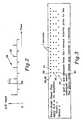
- Fig. 1is a functional block diagram of a fiber optic gyro controller embodying the present invention.
- Fig. 2is wave form showing the transients produced in the photo diode output from the phase modulation.
- Fig. 3is a timing chart showing the production, on cyclically basis of the signals and values used to remove the drift error according to the present invention.
- Fig. 4shows the detector power as a function of phase.
- Fig. 5shows an alternative embodiment for providing a feedback signal to reduce the detector offset.
- the optical path 10corresponds functionally to block 10 in U.S. patent 5,513,003 except for the modulator 50 therein, which corresponds with the phase modulator block 12.
- a D/A 14provides a control signal S1, to control the phase modulation, that includes a square wave, which, it should be understood is the sum of the signals on lines 109 and 119 in U.S. patent 5,513, 003.
- the output S2 from the optical pathis applied to a photo-diode 16, whose output response is shown in Fig. 4.
- the forced phase shift in the lightmoves the output point on the curve between opposite sides of the peak at 203, which produces the transients or spikes S4, shown in Fig. 2, which are spaced apart by ⁇ .
- the controllercontains a signal processor 20 that is programmed to carry out operations to produce a digital signal D1 based on the "Fiber Optic Gyro Equations" operation to produce the signal S1 as a function of the "FOG Information Signal” at block 20a.
- Those program operationsare known in the art and have been shown as software blocks 20a and 20b in the signal processor 20 where they are carried out by suitable processor programming.
- the cyclical production of the signal D1every ⁇ seconds twice the proper frequency.
- the A/D converter 22receives an output from a differential DC amplifier 24, having as one of its inputs the signal S4 from the photo diode PD.
- the other input da_outis applied to the inverted or negative input on the amplifier 24 from a D/A 30, da_out manifesting the analog value of a digital signal da_in that is supplied from the signal processor 20 using the computation 32.
- Da_inis computed at each sampling time using the value su, which is the sum of the current u and previous value u'.
- the value suis multiplied by control constant k with the result summed with the current value of da_in to provide an updated value of da_in.
- the resulting value da_outis subtracted from the value of S4 at the amplifier 24 to produce the value dc_out that is supplied to the A/D 22.
- da_outas discrete analog signal, it can comprise the output from an integrator 50 that receives a one bit word 52 with one of three values, zero or +/- one, depending on the magnitude of da_in. Depending on the successive values of the word 52, produced every ⁇ seconds, da_out would increase or decrease.
Landscapes
- Physics & Mathematics (AREA)
- Engineering & Computer Science (AREA)
- Optics & Photonics (AREA)
- Electromagnetism (AREA)
- Power Engineering (AREA)
- General Physics & Mathematics (AREA)
- Radar, Positioning & Navigation (AREA)
- Remote Sensing (AREA)
- Gyroscopes (AREA)
Description
Claims (6)
- A fiber optic gyro comprising a signal processor (20) and an A/D converter (22) to control thephase of a light applied to an optical phase detector (PD) supplying a signal to the A/Dconverter (22) ,characterized in that:the signal processor (20) comprises means (32) for producing first signals thatrepresent the sum of a second signal and a third signal, the second signal being theoutput (u) from the A/D converter at a first time, the third signal being the outputfrom the AID converter at a second subsequent time (u'); anddifferential amplifier means (24) connected with its inputs to the first signaland the output from the phase detector and supplying at its output a fourth signal tothe A/D converter.
- The fiber optic gyro according to claim 1, furthercharacterizedin that:the interval between the first and second times is the transit time oflight in an optical path (10) carrying light applied to the optical phase detector (PD).
- The fiber optic gyro according to claim 2, further
characterized in that:the time between the first signals is an even integer multiple of theinterval between the first and second times. - The fiber optic gyro according to claim 1, furthercharacterizedby:integration means (50) for producing the first signal by integrating asignal based on the sum of the second and third signals.
- A method of operating a fiber optic gyro according to any preceding claim, comprising a signal processor (20) to control the phase of light applied over a fiber optic path (10) to a phase detector(PD) that produces an output signal (S4) supplied via an A/D converter (22) to saidsignal processor (20),characterized by:producing from the output signal (S4) from the phase detector a phasesignal manifesting a detected phase shift in the light and a bias signal manifestingmodulation of the light;modulating (12) the light to change the phase relationship of the light toprovide a selected power for the light as a function of the phase signal;sampling (32) the output signal from the phase detector at successiveintervals to determine a difference in the output signal between successive intervals; andproviding an offset signal (da-out) to the output signal (S4) from thephase detector as function of said difference to reduce the bias signal, the magnitude ofsaid offset signal increasing on each successive time interval.
- The method described in claim 5, furthercharacterized inthat:the duration of each successive interval is the transit time for light inthe fiber optic path.
Applications Claiming Priority (3)
| Application Number | Priority Date | Filing Date | Title |
|---|---|---|---|
| US771092 | 1985-08-30 | ||
| US08/771,092US5812263A (en) | 1996-12-20 | 1996-12-20 | Accuracy of a fiber optic gyro |
| PCT/US1997/021727WO1998028596A1 (en) | 1996-12-20 | 1997-11-21 | Accuracy of a fiber optic gyro |
Publications (2)
| Publication Number | Publication Date |
|---|---|
| EP0946858A1 EP0946858A1 (en) | 1999-10-06 |
| EP0946858B1true EP0946858B1 (en) | 2002-01-23 |
Family
ID=25090686
Family Applications (1)
| Application Number | Title | Priority Date | Filing Date |
|---|---|---|---|
| EP97954024AExpired - LifetimeEP0946858B1 (en) | 1996-12-20 | 1997-11-21 | Accuracy of a fiber optic gyro |
Country Status (6)
| Country | Link |
|---|---|
| US (1) | US5812263A (en) |
| EP (1) | EP0946858B1 (en) |
| JP (1) | JP2001507132A (en) |
| CA (1) | CA2274891A1 (en) |
| DE (1) | DE69710097T2 (en) |
| WO (1) | WO1998028596A1 (en) |
Families Citing this family (4)
| Publication number | Priority date | Publication date | Assignee | Title |
|---|---|---|---|---|
| US7515271B2 (en)* | 2006-04-03 | 2009-04-07 | Honeywell International Inc. | Wavelength calibration in a fiber optic gyroscope |
| US20080079946A1 (en)* | 2006-09-29 | 2008-04-03 | Honeywell International, Inc. | Digital intensity suppression for vibration and radiation insensitivity in a fiber optic gyroscope |
| US8213018B2 (en)* | 2010-11-10 | 2012-07-03 | Honeywell International Inc. | Constant optical power sensor using a light source current servo combined with digital demodulation intensity suppression for radiation and vibration insensitivity in a fiber optic gyroscope |
| RU2500989C2 (en)* | 2011-12-16 | 2013-12-10 | Федеральное государственное унитарное предприятие "Центр эксплуатации объектов наземной космической инфракструктуры" (ФГУП "ЦЭНКИ") | Electronic unit for fibre-optic gyroscope |
Family Cites Families (4)
| Publication number | Priority date | Publication date | Assignee | Title |
|---|---|---|---|---|
| FR2612300B1 (en)* | 1987-03-13 | 1989-05-26 | Thomson Csf | OPTICAL SIGNAL REJECTION FILTER AND APPLICATIONS TO RING INTERFEROMETERS |
| US5159575A (en)* | 1990-07-02 | 1992-10-27 | Winston Jr Charles R | Single stage demodulator with reference signal phase dither |
| US5513003A (en)* | 1994-06-06 | 1996-04-30 | Honeywell Inc. | Fiber optic gyro digital control with rate extension |
| US5430545A (en)* | 1994-06-21 | 1995-07-04 | Alliedsignal Inc. | Fiber optic angular rate sensor including arrangement for reducing output signal distortion |
- 1996
- 1996-12-20USUS08/771,092patent/US5812263A/ennot_activeExpired - Lifetime
- 1997
- 1997-11-21DEDE69710097Tpatent/DE69710097T2/ennot_activeExpired - Lifetime
- 1997-11-21JPJP52875698Apatent/JP2001507132A/enactivePending
- 1997-11-21WOPCT/US1997/021727patent/WO1998028596A1/enactiveIP Right Grant
- 1997-11-21CACA002274891Apatent/CA2274891A1/ennot_activeAbandoned
- 1997-11-21EPEP97954024Apatent/EP0946858B1/ennot_activeExpired - Lifetime
Also Published As
| Publication number | Publication date |
|---|---|
| JP2001507132A (en) | 2001-05-29 |
| US5812263A (en) | 1998-09-22 |
| CA2274891A1 (en) | 1998-07-02 |
| DE69710097T2 (en) | 2002-08-29 |
| DE69710097D1 (en) | 2002-03-14 |
| EP0946858A1 (en) | 1999-10-06 |
| WO1998028596A1 (en) | 1998-07-02 |
Similar Documents
| Publication | Publication Date | Title |
|---|---|---|
| US5814808A (en) | Optical displacement measuring system using a triangulation including a processing of position signals in a time sharing manner | |
| US5684591A (en) | Fiber optic gyroscope with reduced non-linearity at low angular rates | |
| CA2026962C (en) | Fiber optic sagnac interferometer with digital phase ramp resetting for measurement of rate of rotation | |
| JPH03210417A (en) | Fiber visual sense measuring device, gyrometer centralized navigation and stabilizing system | |
| US5080489A (en) | Fiber optic gyroscope for detecting angular velocity of rotation using equivalent time sampling | |
| US9557175B2 (en) | Fiber optic gyroscope dead band error suppression | |
| CA2031175C (en) | Fiber optic gyro system using sample and hold units for wide angle accomodation | |
| EP0511684B1 (en) | Phase modulated fibre-optic gyroscope | |
| EP0946858B1 (en) | Accuracy of a fiber optic gyro | |
| US5363195A (en) | Automatic gain calibration system for a phase modulator in a fiber optic gyro | |
| CA2061904C (en) | Phase modulated fiber optic gyro accommodating angular rate reversals | |
| CA2058311C (en) | Fiber optic gyro | |
| EP0412468B1 (en) | Synthetic serrodyne controller for fiber optic gyroscope | |
| US5182611A (en) | Digital synthetic serrodyne for fiber optic gyroscope | |
| JP2660573B2 (en) | Optical interference angular velocity meter | |
| CN1205430A (en) | Rate control loop for fiber optic gyroscope | |
| JPH0293319A (en) | fiber optic gyro | |
| JPH04369421A (en) | Optical fiber gyro | |
| JPH01124704A (en) | Linearizing circuit | |
| JPH01207620A (en) | fiber optic gyroscope | |
| JPH11295077A (en) | Optical interference angular velocity meter | |
| JPH1123289A (en) | Optical interference angular velocity meter | |
| JPH087070B2 (en) | Phase modulation optical fiber gyro |
Legal Events
| Date | Code | Title | Description |
|---|---|---|---|
| PUAI | Public reference made under article 153(3) epc to a published international application that has entered the european phase | Free format text:ORIGINAL CODE: 0009012 | |
| 17P | Request for examination filed | Effective date:19990719 | |
| AK | Designated contracting states | Kind code of ref document:A1 Designated state(s):DE FR GB SE | |
| GRAG | Despatch of communication of intention to grant | Free format text:ORIGINAL CODE: EPIDOS AGRA | |
| GRAG | Despatch of communication of intention to grant | Free format text:ORIGINAL CODE: EPIDOS AGRA | |
| GRAH | Despatch of communication of intention to grant a patent | Free format text:ORIGINAL CODE: EPIDOS IGRA | |
| GRAH | Despatch of communication of intention to grant a patent | Free format text:ORIGINAL CODE: EPIDOS IGRA | |
| 17Q | First examination report despatched | Effective date:20010515 | |
| GRAA | (expected) grant | Free format text:ORIGINAL CODE: 0009210 | |
| REG | Reference to a national code | Ref country code:GB Ref legal event code:IF02 | |
| AK | Designated contracting states | Kind code of ref document:B1 Designated state(s):DE FR GB SE | |
| REF | Corresponds to: | Ref document number:69710097 Country of ref document:DE Date of ref document:20020314 | |
| ET | Fr: translation filed | ||
| PLBE | No opposition filed within time limit | Free format text:ORIGINAL CODE: 0009261 | |
| STAA | Information on the status of an ep patent application or granted ep patent | Free format text:STATUS: NO OPPOSITION FILED WITHIN TIME LIMIT | |
| 26N | No opposition filed | ||
| PGFP | Annual fee paid to national office [announced via postgrant information from national office to epo] | Ref country code:GB Payment date:20051004 Year of fee payment:9 | |
| PGFP | Annual fee paid to national office [announced via postgrant information from national office to epo] | Ref country code:SE Payment date:20051107 Year of fee payment:9 | |
| PG25 | Lapsed in a contracting state [announced via postgrant information from national office to epo] | Ref country code:SE Free format text:LAPSE BECAUSE OF NON-PAYMENT OF DUE FEES Effective date:20061122 | |
| EUG | Se: european patent has lapsed | ||
| GBPC | Gb: european patent ceased through non-payment of renewal fee | Effective date:20061121 | |
| PG25 | Lapsed in a contracting state [announced via postgrant information from national office to epo] | Ref country code:GB Free format text:LAPSE BECAUSE OF NON-PAYMENT OF DUE FEES Effective date:20061121 | |
| REG | Reference to a national code | Ref country code:FR Ref legal event code:PLFP Year of fee payment:19 | |
| PGFP | Annual fee paid to national office [announced via postgrant information from national office to epo] | Ref country code:DE Payment date:20151130 Year of fee payment:19 | |
| REG | Reference to a national code | Ref country code:FR Ref legal event code:PLFP Year of fee payment:20 | |
| PGFP | Annual fee paid to national office [announced via postgrant information from national office to epo] | Ref country code:FR Payment date:20161017 Year of fee payment:20 | |
| REG | Reference to a national code | Ref country code:DE Ref legal event code:R119 Ref document number:69710097 Country of ref document:DE | |
| PG25 | Lapsed in a contracting state [announced via postgrant information from national office to epo] | Ref country code:DE Free format text:LAPSE BECAUSE OF NON-PAYMENT OF DUE FEES Effective date:20170601 | |
| P01 | Opt-out of the competence of the unified patent court (upc) registered | Effective date:20230525 |