EP0935279A2 - Device and method for load locking for semiconductuctor processing - Google Patents
Device and method for load locking for semiconductuctor processingDownload PDFInfo
- Publication number
- EP0935279A2 EP0935279A2EP99200381AEP99200381AEP0935279A2EP 0935279 A2EP0935279 A2EP 0935279A2EP 99200381 AEP99200381 AEP 99200381AEP 99200381 AEP99200381 AEP 99200381AEP 0935279 A2EP0935279 A2EP 0935279A2
- Authority
- EP
- European Patent Office
- Prior art keywords
- chamber
- wafer holding
- holding means
- processed
- objects
- Prior art date
- Legal status (The legal status is an assumption and is not a legal conclusion. Google has not performed a legal analysis and makes no representation as to the accuracy of the status listed.)
- Withdrawn
Links
- 238000000034methodMethods0.000titleclaimsdescription16
- 230000007723transport mechanismEffects0.000claimsabstractdescription34
- 238000007789sealingMethods0.000claimsabstractdescription6
- 230000003028elevating effectEffects0.000claimsdescription6
- 235000012431wafersNutrition0.000description107
- 239000004065semiconductorSubstances0.000description46
- 230000007246mechanismEffects0.000description11
- 230000008569processEffects0.000description6
- 230000032258transportEffects0.000description6
- 239000010409thin filmSubstances0.000description3
- 230000000694effectsEffects0.000description2
- 238000004519manufacturing processMethods0.000description2
- 230000009467reductionEffects0.000description2
- 230000003416augmentationEffects0.000description1
- 238000004891communicationMethods0.000description1
- 238000005530etchingMethods0.000description1
- 239000000463materialSubstances0.000description1
- 238000002230thermal chemical vapour depositionMethods0.000description1
Images


Classifications
- H—ELECTRICITY
- H01—ELECTRIC ELEMENTS
- H01L—SEMICONDUCTOR DEVICES NOT COVERED BY CLASS H10
- H01L21/00—Processes or apparatus adapted for the manufacture or treatment of semiconductor or solid state devices or of parts thereof
- H01L21/67—Apparatus specially adapted for handling semiconductor or electric solid state devices during manufacture or treatment thereof; Apparatus specially adapted for handling wafers during manufacture or treatment of semiconductor or electric solid state devices or components ; Apparatus not specifically provided for elsewhere
- H01L21/68—Apparatus specially adapted for handling semiconductor or electric solid state devices during manufacture or treatment thereof; Apparatus specially adapted for handling wafers during manufacture or treatment of semiconductor or electric solid state devices or components ; Apparatus not specifically provided for elsewhere for positioning, orientation or alignment
- H—ELECTRICITY
- H01—ELECTRIC ELEMENTS
- H01L—SEMICONDUCTOR DEVICES NOT COVERED BY CLASS H10
- H01L21/00—Processes or apparatus adapted for the manufacture or treatment of semiconductor or solid state devices or of parts thereof
- H01L21/67—Apparatus specially adapted for handling semiconductor or electric solid state devices during manufacture or treatment thereof; Apparatus specially adapted for handling wafers during manufacture or treatment of semiconductor or electric solid state devices or components ; Apparatus not specifically provided for elsewhere
- H01L21/677—Apparatus specially adapted for handling semiconductor or electric solid state devices during manufacture or treatment thereof; Apparatus specially adapted for handling wafers during manufacture or treatment of semiconductor or electric solid state devices or components ; Apparatus not specifically provided for elsewhere for conveying, e.g. between different workstations
- H01L21/67739—Apparatus specially adapted for handling semiconductor or electric solid state devices during manufacture or treatment thereof; Apparatus specially adapted for handling wafers during manufacture or treatment of semiconductor or electric solid state devices or components ; Apparatus not specifically provided for elsewhere for conveying, e.g. between different workstations into and out of processing chamber
- H01L21/67748—Apparatus specially adapted for handling semiconductor or electric solid state devices during manufacture or treatment thereof; Apparatus specially adapted for handling wafers during manufacture or treatment of semiconductor or electric solid state devices or components ; Apparatus not specifically provided for elsewhere for conveying, e.g. between different workstations into and out of processing chamber horizontal transfer of a single workpiece
- H—ELECTRICITY
- H01—ELECTRIC ELEMENTS
- H01L—SEMICONDUCTOR DEVICES NOT COVERED BY CLASS H10
- H01L21/00—Processes or apparatus adapted for the manufacture or treatment of semiconductor or solid state devices or of parts thereof
- H01L21/67—Apparatus specially adapted for handling semiconductor or electric solid state devices during manufacture or treatment thereof; Apparatus specially adapted for handling wafers during manufacture or treatment of semiconductor or electric solid state devices or components ; Apparatus not specifically provided for elsewhere
- H01L21/677—Apparatus specially adapted for handling semiconductor or electric solid state devices during manufacture or treatment thereof; Apparatus specially adapted for handling wafers during manufacture or treatment of semiconductor or electric solid state devices or components ; Apparatus not specifically provided for elsewhere for conveying, e.g. between different workstations
- H01L21/67739—Apparatus specially adapted for handling semiconductor or electric solid state devices during manufacture or treatment thereof; Apparatus specially adapted for handling wafers during manufacture or treatment of semiconductor or electric solid state devices or components ; Apparatus not specifically provided for elsewhere for conveying, e.g. between different workstations into and out of processing chamber
- H01L21/67751—Apparatus specially adapted for handling semiconductor or electric solid state devices during manufacture or treatment thereof; Apparatus specially adapted for handling wafers during manufacture or treatment of semiconductor or electric solid state devices or components ; Apparatus not specifically provided for elsewhere for conveying, e.g. between different workstations into and out of processing chamber vertical transfer of a single workpiece
- Y—GENERAL TAGGING OF NEW TECHNOLOGICAL DEVELOPMENTS; GENERAL TAGGING OF CROSS-SECTIONAL TECHNOLOGIES SPANNING OVER SEVERAL SECTIONS OF THE IPC; TECHNICAL SUBJECTS COVERED BY FORMER USPC CROSS-REFERENCE ART COLLECTIONS [XRACs] AND DIGESTS
- Y10—TECHNICAL SUBJECTS COVERED BY FORMER USPC
- Y10S—TECHNICAL SUBJECTS COVERED BY FORMER USPC CROSS-REFERENCE ART COLLECTIONS [XRACs] AND DIGESTS
- Y10S414/00—Material or article handling
- Y10S414/135—Associated with semiconductor wafer handling
- Y10S414/137—Associated with semiconductor wafer handling including means for charging or discharging wafer cassette
- Y—GENERAL TAGGING OF NEW TECHNOLOGICAL DEVELOPMENTS; GENERAL TAGGING OF CROSS-SECTIONAL TECHNOLOGIES SPANNING OVER SEVERAL SECTIONS OF THE IPC; TECHNICAL SUBJECTS COVERED BY FORMER USPC CROSS-REFERENCE ART COLLECTIONS [XRACs] AND DIGESTS
- Y10—TECHNICAL SUBJECTS COVERED BY FORMER USPC
- Y10S—TECHNICAL SUBJECTS COVERED BY FORMER USPC CROSS-REFERENCE ART COLLECTIONS [XRACs] AND DIGESTS
- Y10S414/00—Material or article handling
- Y10S414/135—Associated with semiconductor wafer handling
- Y10S414/139—Associated with semiconductor wafer handling including wafer charging or discharging means for vacuum chamber
- Y—GENERAL TAGGING OF NEW TECHNOLOGICAL DEVELOPMENTS; GENERAL TAGGING OF CROSS-SECTIONAL TECHNOLOGIES SPANNING OVER SEVERAL SECTIONS OF THE IPC; TECHNICAL SUBJECTS COVERED BY FORMER USPC CROSS-REFERENCE ART COLLECTIONS [XRACs] AND DIGESTS
- Y10—TECHNICAL SUBJECTS COVERED BY FORMER USPC
- Y10S—TECHNICAL SUBJECTS COVERED BY FORMER USPC CROSS-REFERENCE ART COLLECTIONS [XRACs] AND DIGESTS
- Y10S414/00—Material or article handling
- Y10S414/135—Associated with semiconductor wafer handling
- Y10S414/141—Associated with semiconductor wafer handling includes means for gripping wafer
Definitions
- the present inventionrelates to a load-lock device which stands by with a plurality of semiconductor wafers loaded thereon to cooperate with a transport device for in order transporting the semiconductor wafers to a processing chamber and, more particularly, to a load-lock device having a structure to transport semiconductor wafers to a processing chamber efficiently.
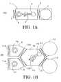
- a conventional semiconductor processing apparatushas employed a load-lock device which stands by with a plurality of semiconductor wafers loaded thereon in order to transport objects to be processed such as semiconductor wafers to a processing chamber in order for processing therein which will be elucidated referring to figure 1A.
- Such a conventional load-lock device having a plurality of chambershas reduced the so-called idle time of the processing chambers to thereby improve productivity.
- the number of load-lock chambersmay be increased in order to avoid this.
- an augmentation in the number of chambersresults in an increase in the time required for opening and closing the gate valves to reduce productivity.
- the conventional structure in which a plurality of load-lock chambers are disposed horizontallyincreases the size of an device as a whole, which goes against the needs in the market for reduction of the space for such an device.
- Conventional load-lock deviceshave such limitations from the view point of hardware.
- a load-lock devicecomprises means as described below.
- a load-lock devicewhich stands by with objects to be processed loaded thereon in order to cooperate with a transport mechanism in transporting the objects to be processed into a processing chamber in order, comprising:
- the transport mechanismis connected to a side of the chamber means substantially in the center thereof.
- the flange meansis coupled to the side of the wafer holding means substantially in the center thereof and, when it is engaged with a part of the inner wall of the chamber, a part of the wafer holding means is completely isolated from the transport mechanism and the remaining part of the wafer holding means is exposed to the transport mechanism.
- the chamberpreferably includes at least one door valve for transporting the objects to be processed into and out of the wafer holding means.
- the wafer holding meansis specifically supported by elevating means.
- the flange meanspreferably includes sealing means.
- the load-lock devicecomprises chamber means, wafer holding means for loading a plurality of the objects to be processed, the wafer holding means being movable up and dawn in the chamber and flange means provided on a side of the wafer holding means, the flange means being engaged with a part of an inner wall of the chamber to divide the space inside the chamber into two isolated rooms, the method comprising the steps of:
- the above-mentioned methodmay further comprise the steps of:
- the engagement between the flange means and a part of the chamber inner wallis maintained during the step of restoring the pressure in the room isolated from the transport mechanism to the atmospheric pressure.
- the front door 5is opened to allow a wafer holding means 6 loaded with the semiconductor wafers 4 to be transported into the chamber 1
- the front door 5is closed to evacuate the interior of the chamber 1.
- the gate valve 3is opened, and the transport mechanism 7 transports one of the semiconductor wafers 4 into the processing chamber 2.
- the semiconductor wafer 4is returned to its initial position in the wafer holding means 6 after being processed in the processing chamber 2, and the next semiconductor wafer 4 is then transported into the processing chamber 2.
- the gate valve 3is closed and the front door 5 is opened to remove the wafer holding means 6 from the chamber 1. Thereafter, another wafer holding means 6 is transported into the chamber 1 through the front door 5.
- FIG. 1Bschematically shows a conventional lock-load device having a plurality of chambers.
- This devicecomprises one transport mechanism 10, two load-lock chambers 8, 9 connected to the transport mechanism 10 through gate valves 12 and two processing chambers 13, 14 connected to the transport mechanism 10 through gate valves 12.
- the chambers 8, 9respectively includes wafer holding means 16, 17 for standing by with a predetermined number of semiconductor wafers loaded thereon and door valves 11A, 11B for transporting processed semiconductors in order out of the chamber.
- the door valves 11A, 11B of the respective load-lock chambers 8, 9are opened to load a predetermined number of semiconductor wafers 18 into the wafer holding means 16, 17 and, thereafter, the interior of the chambers 8, 9 are evacuated. Then, a first gate valve 12A is opened to transport the semiconductor wafer 18 from the first load-lock chamber 8 to the processing chambers 13, 14 in order. When the process is completed, the semiconductor wafers 18 in the processing chambers 13, 14 are returned to the first load-lock chamber 8, and the first gate valve 12A is closed. Thereafter, a second gate valve 12B is opened to transport the semiconductor wafers 18 from the second load-lock chamber 9 to the processing chambers 13, 14 in order. Meanwhile, the door valve 11A of the first load-lock chamber 8 is opened to remove the processed semiconductor wafers in order and to load the next semiconductor wafers in the wafer holding means 16.
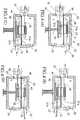
- Fig. 2is a schematic plan view of a semiconductor manufacturing apparatus including a load-lock device according to the present invention.
- the apparatuscomprises a transport mechanism 24 in the middle thereof, a load-lock device 20 according to the invention connected to the transport mechanism 24 and four processing chambers 22 connected around the transport mechanism 24 through gate valves 23. It should be noted here that no gate valve intervenes between a load-lock chamber 25 and the transport mechanism 24 as will be described later in detail. This is the most significant feature of the present invention.
- the transport mechanism 24is a normal arm type mechanism.
- the processing chambers 22are thermal CVD apparatuses or etching apparatuses.
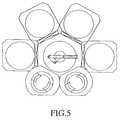
- load-lock device 20comprises one load-lock chamber 25 in the preferred embodiment, it is possible to use two load-lock chambers provided adjacent to each other in the horizontal direction as shown in Fig. 5. Similarly, two or more load-lock chambers may be used.
- Figs. 3A and 3Bshow sectional views of the apparatus shown in Fig. 2.
- Figs. 3A and 3Bshow sectional views taken along the lines A-A and B-B indicated in Fig. 2, respectively.
- the load-lock device 20which stands by with semiconductor wafers loaded thereon in order to cooperate with the transporting mechanism for transporting the semiconductor wafers to the processing chambers in order comprises the chamber 25, wafer holding means 31 for loading semiconductor wafers 38 which is movable up and down in the chamber 25 and flange means 30 provided on a side of the wafer holding means 31 which is engaged with a contact portion 36 on the inner wall of the chamber to divide the space inside the chamber 25 into two isolated rooms X and Y.
- the transport mechanism 24is connected to substantially in the center of the chamber 25 and the semiconductor wafer 38 loaded on the wafer holding means 31 are transported to the processing chambers 22 by an arm mechanism 35.
- two door valves 32, 33are provided on a side of the chamber 25, and the semiconductor wafers 38 are loaded into and unloaded from the wafer holding means 31 through the door valves by an external arm mechanism 39.
- the door valves 32, 33may function as outlet and inlet ports.
- the chamber 25may include a separate outlet and/or inlet port for evacuating the interior of the chamber and/or taking air into there.
- the wafer holding means 31preferably comprises pairs of left and right supports 31d, 31d', 31e, 31e' and a plurality of loading portion 31c on which wafers are loaded.
- the wafer holding means 31is divided by the flange means 30 into two upper and lower sections 31a and 31b.
- the number of the semiconductor wafers 38 loaded in the wafer holding means 31depends on the number of the processing chambers 22 connected to the load-lock device and the kinds of the process, and an appropriate number is chosen by taking productivity into consideration.
- the wafer holding means 31is supported by an elevating means 34 connected to an external driving device (not shown) and is movable up and down in the chamber 25.
- the flange means 30is a disc made of a material which is not easily deformed and is coupled substantially to the center of the wafer holding means 31.
- the periphery of the flange means 30comes into engage with the contact portion 36 on the inner wall of the chamber 25.
- a sealing member 37is provided at the periphery of the flange means and/or the contact portion 36 on the chamber inner wall.
- the above-mentioned contact portion 36may be a flange extending inside the chamber 25. In this case, the periphery of the flange means 30 is engaged with the flange provided on the inner wall of the chamber 25.
- FIGs. 4A through 4Dschematically show sectional views of the load-lock device according to the present invention.
- Figs. 4A and 4Dshow the wafer holding means 31 in the upper limit position
- Figs. 4B and 4Cshow the wafer holing means 31 in a lower limit position.
- a method for transporting and removing semiconductor wafers loaded in a chamber to and from predetermined processing chambers in order using the load-lock device 20 according to the inventioncomprises the steps of:
- An appropriate valueis chosen for the number of semiconductor wafers loaded in the upper section 31a and lower section 31b of the wafer holding means 31 depending on the number of the processing chambers and the kinds of the process.
- the atmospheric pressureis restored in the rooms as the door valves 32, 33 are opened and, as a result, the flange means 30 is subjected to a pressure that acts opposite to the direction of the engagement.
- the elevating means 34preferably holds retains the wafer holding means to maintain the sealing.
- the flange means 30functions as a valve, it is possible to remove a gate valve which has been conventionally required between the transport mechanism 24 and load-lock chamber 25. This makes it possible to reduce the time required for opening and closing the gate valve, thereby improving productivity.
- the removement of the gate valvemakes it possible to eliminate a structure at a gate valve mounting area which has been provided on the inner wall of the chamber. As a result, the distance between the transport mechanism and load-lock chamber can be reduced by at least about 120 mm to achieve reduction of the dimension of the apparatus.
- a load-lock device according to the inventionhas operations and effects substantially equivalent to those of a conventional load-lock device having two load-lock chambers arranged horizontally, the present invention allows one load-lock chamber as viewed in a plan view to achieve the same effect as that of two chambers. As a result, the area occupied by a transport mechanism and a load-lock device can be reduced by about 40 %.
- conventional load-lock deviceshave had a problem in that processing chambers can be stopped due to delay of replacement of objects to be processed in the case of thin film processing which is performed in a short processing time and when a number of processing chambers are used.
- the use of two load-lock devices according to the inventionmakes it possible to solve this easily because they substantially serve as four load-lock chambers.
- the inventionallows productivity to be improved by about 30 % compared to a conventional load-lock device in the case of thin film processing in which three processing chambers are used and the processing time is about 40 seconds.
Landscapes
- Engineering & Computer Science (AREA)
- Physics & Mathematics (AREA)
- Condensed Matter Physics & Semiconductors (AREA)
- General Physics & Mathematics (AREA)
- Manufacturing & Machinery (AREA)
- Computer Hardware Design (AREA)
- Microelectronics & Electronic Packaging (AREA)
- Power Engineering (AREA)
- Container, Conveyance, Adherence, Positioning, Of Wafer (AREA)
Abstract
Description
The present invention relates to a load-lockdevice which stands by with a plurality of semiconductorwafers loaded thereon to cooperate with atransport device for in order transporting the semiconductorwafers to a processing chamber and, moreparticularly, to a load-lock device having a structureto transport semiconductor wafers to a processingchamber efficiently.
A conventional semiconductor processing apparatushas employed a load-lock device which stands by with aplurality of semiconductor wafers loaded thereon inorder to transport objects to be processed such assemiconductor wafers to a processing chamber in orderfor processing therein which will be elucidatedreferring to figure 1A.
However, such a conventional single chamber typeload-lock device has had the problem of low productivitybecause the processing apparatus must bestopped during the time required for replacing waferholding means.
Under such circumstances, load-lock deviceshaving a plurality of chambers have been developed toimprove productivity. This will be elucidated referringto figure 1A.
Such a conventional load-lock device having a pluralityof chambers has reduced the so-called idle time of the processingchambers to thereby improve productivity.
However, such a conventional load-lock device having aplurality of chambers has problems as described below.
In a conventional load-lock device having a plurality ofchambers, in order to improve the rate of operation of theprocessing chambers, while semiconductor wafers in the firstload-lock chamber are processed, processed semiconductors mustbe removed from the second load-lock chamber to load newsemiconductor wafers therein and the door valve must be closedto evacuate the second load-lock chamber to put in a stand-bystate. If this operation can not be carried out while thesemiconductor wafers are being processed, new semiconductorwafers can not be transported into the processing chambers inspite of which the process has already been completed, whichleaves the processing chambers in a vacant state. Such a riskis significant especially for processes such as thin filmprocessing which are performed in a short processing time. Thesame situation is likely to occur when a great number of chambersare used.
The number of load-lock chambers may be increased in orderto avoid this. However, in a conventional load-lock devicehaving a plurality of chambers in which gate valves intervenebetween each of the load-lock chambers and the transport mechanism, an augmentation in the number of chambers results inan increase in the time required for opening and closing the gatevalves to reduce productivity. In addition, the conventionalstructure in which a plurality of load-lock chambers are disposedhorizontally increases the size of an device as a whole, whichgoes against the needs in the market for reduction of the spacefor such an device. Conventional load-lock devices have suchlimitations from the view point of hardware.
It is therefore an object of the invention to provide aload-lock device and a method in which the space for an devicecan be reduced and productivity can be improved.
It is another object of the invention to provide a load-lockdevice and a therefor in which high productivity can be maintainedeven for many processing chambers and processes performed in ashort processing time.
In order to achieve the above-mentioned objects, aload-lock device according to the present invention comprisesmeans as described below.
There is provided a load-lock device which stands by withobjects to be processed loaded thereon in order to cooperate witha transport mechanism in transporting the objects to be processedinto a processing chamber in order, comprising:
Preferably, the transport mechanism is connected to a sideof the chamber means substantially in the center thereof.
Preferably, the flange means is coupled to the side of thewafer holding means substantially in the center thereof and, whenit is engaged with a part of the inner wall of the chamber, apart of the wafer holding means is completely isolated from thetransport mechanism and the remaining part of the wafer holdingmeans is exposed to the transport mechanism.
Further, the chamber preferably includes at least one doorvalve for transporting the objects to be processed into and outof the wafer holding means.
The wafer holding means is specifically supported byelevating means.
Furthermore, the flange means preferably includes sealingmeans.
There is provided a method for transporting objects to beprocessed loaded and kept in a load-lock device to and frompredetermined processing chambers in order wherein the load-lockdevice comprises chamber means, wafer holding means for loading a plurality of the objects to be processed, the waferholding means being movable up and dawn in the chamber and flangemeans provided on a side of the wafer holding means, the flangemeans being engaged with a part of an inner wall of the chamberto divide the space inside the chamber into two isolated rooms,the method comprising the steps of:
The above-mentioned method may further comprise the stepsof:
Preferably, the engagement between the flange means anda part of the chamber inner wall is maintained during the stepof restoring the pressure in the room isolated from the transportmechanism to the atmospheric pressure.
The present invention will now be described indetail with reference to the accompanying drawings,wherein:
After the front door 5 is opened to allow awafer holdingmeans 6 loaded with the semiconductor wafers 4 to be transportedinto the chamber 1, the front door 5 is closed to evacuate theinterior of the chamber 1. Then, thegate valve 3 is opened, andthetransport mechanism 7 transports one of the semiconductor wafers 4 into theprocessing chamber 2. Thesemiconductor wafer 4 is returned to its initial position in thewafer holding means 6 after being processed in theprocessing chamber 2, and thenextsemiconductor wafer 4 is then transported into theprocessingchamber 2. When all of the semiconductor wafers 4 in thewaferholding means 6 are thus processed, thegate valve 3 is closedand the front door 5 is opened to remove thewafer holding means 6 from the chamber 1. Thereafter, anotherwafer holding means 6 is transported into the chamber 1 through the front door 5.
However, such a conventional single chamber type load-lockdevice has had the problem of low productivity because theprocessing apparatus must be stopped during the time requiredfor replacing wafer holding means. It will be elucidatedreferring to Fig. 1B.
Under such circumstances, load- lock devices having aplurality of chambers have been developed to improve productivity.Fig. 1B schematically shows a conventional lock-load devicehaving a plurality of chambers. This device comprises onetransport mechanism 10, two load-lock chambers 8, 9 connectedto thetransport mechanism 10 throughgate valves 12 and twoprocessing chambers transport mechanism 10 throughgate valves 12. Thechambers 8, 9 respectivelyincludeswafer holding means door valves
Thedoor valves lockchambers 8, 9 are opened to load a predetermined number ofsemiconductor wafers 18 into thewafer holding means chambers 8, 9 are evacuated. Then,afirst gate valve 12A is opened to transport thesemiconductorwafer 18 from the first load-lock chamber 8 to theprocessingchambers semiconductor wafers 18 in theprocessing chambers lock chamber 8, and thefirst gatevalve 12A is closed. Thereafter, asecond gate valve 12B isopened to transport thesemiconductor wafers 18 from the secondload-lock chamber 9 to theprocessing chambers door valve 11A of the first load-lock chamber 8is opened to remove the processed semiconductor wafers in orderand to load the next semiconductor wafers in the wafer holdingmeans 16.
Fig. 2 is a schematic plan view of a semiconductormanufacturing apparatus including a load-lock device accordingto the present invention. The apparatus comprises atransportmechanism 24 in the middle thereof, a load-lock device 20according to the invention connected to thetransport mechanism 24 and fourprocessing chambers 22 connected around thetransportmechanism 24 throughgate valves 23. It should be noted here thatno gate valve intervenes between a load-lock chamber 25 and thetransport mechanism 24 as will be described later in detail. Thisis the most significant feature of the present invention. Thetransport mechanism 24 is a normal arm type mechanism. Forexample, theprocessing chambers 22 are thermal CVD apparatusesor etching apparatuses. While the load-lock device 20 according to the invention comprises one load-lock chamber 25 in thepreferred embodiment, it is possible to use two load-lockchambers provided adjacent to each other in the horizontaldirection as shown in Fig. 5. Similarly, two or more load-lockchambers may be used.
Figs. 3A and 3B show sectional views of the apparatus shownin Fig. 2. Figs. 3A and 3B show sectional views taken along thelines A-A and B-B indicated in Fig. 2, respectively.
The load-lock device 20 which stands by with semiconductorwafers loaded thereon in order to cooperate with the transportingmechanism for transporting the semiconductor wafers to theprocessing chambers in order comprises thechamber 25, waferholding means 31 for loadingsemiconductor wafers 38 which ismovable up and down in thechamber 25 and flange means 30 providedon a side of the wafer holding means 31 which is engaged withacontact portion 36 on the inner wall of the chamber to dividethe space inside thechamber 25 into two isolated rooms X andY.
Thetransport mechanism 24 is connected to substantiallyin the center of thechamber 25 and thesemiconductor wafer 38loaded on the wafer holding means 31 are transported to theprocessing chambers 22 by anarm mechanism 35. Preferably, twodoor valves chamber 25, andthesemiconductor wafers 38 are loaded into and unloaded fromthe wafer holding means 31 through the door valves by anexternal arm mechanism 39. Thedoor valves chamber 25 may include a separate outletand/or inlet port for evacuating the interior of the chamberand/or taking air into there.
The wafer holding means 31 preferably comprises pairs ofleft andright supports loading portion 31c on which wafers are loaded. The wafer holdingmeans 31 is divided by the flange means 30 into two upper andlower sections semiconductorwafers 38 loaded in the wafer holding means 31 depends on thenumber of theprocessing chambers 22 connected to the load-lockdevice and the kinds of the process, and an appropriate numberis chosen by taking productivity into consideration. The waferholding means 31 is supported by an elevatingmeans 34 connectedto an external driving device (not shown) and is movable up anddown in thechamber 25.
Preferably, the flange means 30 is a disc made of a materialwhich is not easily deformed and is coupled substantially to thecenter of the wafer holding means 31. When the wafer holdingmeans 31 is elevated by the elevating means 34 to an upper limitposition, the periphery of the flange means 30 comes into engagewith thecontact portion 36 on the inner wall of thechamber 25.Preferably, a sealingmember 37 is provided at the periphery ofthe flange means and/or thecontact portion 36 on the chamberinner wall. As a result, theupper section 31a of the wafer holding means 31 is completely isolated from thetransportmechanism 24 and, at the same time, thelower section 31b of thewafer holding means 31 is exposed to thetransport mechanism 24.Alternatively, the above-mentionedcontact portion 36 may be aflange extending inside thechamber 25. In this case, theperiphery of the flange means 30 is engaged with the flangeprovided on the inner wall of thechamber 25.
The operation of the load-lock device according to theinvention will now be described. Figs. 4A through 4Dschematically show sectional views of the load-lock deviceaccording to the present invention. Figs. 4A and 4D show thewafer holding means 31 in the upper limit position, and Figs.4B and 4C show the wafer holing means 31 in a lower limit position.
A method for transporting and removing semiconductorwafers loaded in a chamber to and from predetermined processingchambers in order using the load-lock device 20 according to theinvention comprises the steps of:
An appropriate value is chosen for the number ofsemiconductor wafers loaded in theupper section 31a andlowersection 31b of the wafer holding means 31 depending on the numberof the processing chambers and the kinds of the process. Duringthe steps of loading semiconductor wafers to the wafer from theoutside of thechamber 25 holding means 31 and transporting themfrom the wafer holding means to the outside of thechamber 25,the atmospheric pressure is restored in the rooms as thedoorvalves
With a load-lock device according to the invention, sincethe flange means 30 functions as a valve, it is possible to removea gate valve which has been conventionally required between thetransport mechanism 24 and load-lock chamber 25. This makes itpossible to reduce the time required for opening and closing thegate valve, thereby improving productivity.
The removement of the gate valve makes it possible to eliminate a structure at a gate valve mounting area which hasbeen provided on the inner wall of the chamber. As a result, thedistance between the transport mechanism and load-lock chambercan be reduced by at least about 120 mm to achieve reduction ofthe dimension of the apparatus.
Further, since a load-lock device according to theinvention has operations and effects substantially equivalentto those of a conventional load-lock device having two load-lockchambers arranged horizontally, the present inventionallows one load-lock chamber as viewed in a plan view to achievethe same effect as that of two chambers. As a result, the areaoccupied by a transport mechanism and a load-lock device can bereduced by about 40 %.
Furthermore, conventional load-lock devices have had aproblem in that processing chambers can be stopped due to delayof replacement of objects to be processed in the case of thinfilm processing which is performed in a short processing timeand when a number of processing chambers are used. The use oftwo load-lock devices according to the invention makes itpossible to solve this easily because they substantially serveas four load-lock chambers. For example, the invention allowsproductivity to be improved by about 30 % compared to aconventional load-lock device in the case of thin film processingin which three processing chambers are used and the processingtime is about 40 seconds.
Claims (9)
- A load-lock device which stands by with objects to beprocessed loaded thereon in order to cooperate with a transportmechanism in transporting said objects to be processed into aprocessing chamber in order, comprising:chamber means;wafer holding means for loading a plurality of saidobjects to be processed, said wafer holding means being movableup and down in said chamber; andflange means provided on a side of said wafer holding means,said flange means being engaged with a part of an inner wall ofsaid chamber to divide the space inside said chamber into twoisolated rooms.
- A device according to Claim 1, wherein said transportmechanism is connected to a side of said chamber meanssubstantially in the center thereof.
- A device according to Claim 2, wherein said flange meansis coupled to the side of said flange means substantially in thecenter thereof and, when it is engaged with a part of the innerwall of said chamber, a part of said wafer holding means iscompletely isolated from said transport mechanism and theremaining part of said wafer holding means is exposed to saidtransport mechanism.
- A device according to any of Claims 1 through 3, whereinsaid chamber preferably includes at least one door valve for transporting said objects to be processed into and out of saidwafer holding means.
- A device according to Claim 1 or 4, wherein said holdingmeans is supported by elevating means.
- A device according to Claim 1 or 5, said flange meansincludes sealing means.
- A method for transporting objects to be processed loadedand kept in a load-lock device to and from predeterminedprocessing chambers in order wherein said load-lock devicecomprises chamber means, wafer holding means for loading aplurality of said objects to be processed, said wafer holdingmeans being movable up and down in said chamber, and flange meansprovided on a side of said wafer holding means, said flange meansbeing engaged with a part of an inner wall of said chamber todivide the space inside said chamber into two isolated rooms,said method comprising the steps of:loading said objects to be processed in a first portionof said wafer holding means with said flange means inengagement and contact therewith in a first position and, in themean time, transporting processed objects from said processingchamber and loading them to a second portion of said wafer holdingmeans;unloading said objects to be processed from the firstportion of said wafer holding member and transporting them tosaid processing chamber with said wafer holding member moved to put said flange means in engagement and contact therewith in asecond position and, in the mean time, unloading said processedobjects from the second portion of said wafer holding means tothe outside of the chamber;loading said objects to be processed in the second portionof said wafer holding means with said flange means in engagementand contact therewith in the second position and, in the meantime, transporting processed objects from another processingchamber and loading them to the first portion of said waferholding means;unloading said objects to be processed from the secondportion of said wafer holding member and transporting them tosaid another processing chamber with said wafer holding membermoved to put said flange means in engagement and contact therewithin the first position and, in the mean time, unloading saidprocessed objects from the first portion of said wafer holdingmeans to the outside of the chamber; andrepeating said steps.
- A method according to Claim 7, further comprising thesteps of:restoring the pressure in the room isolated from saidtransport mechanism to the atmospheric pressure during theloading of objects to be processed into said wafer holding meansor the unload of the same to the outside of the chamber; andevacuating the room isolated from said transport mechanism after either loading said objects to be processed intosaid wafer holding means or unloading them from said wafer holdingmeans is completed.
- A method according to Claim 8, wherein the engagementbetween said flange means and a part of said chamber inner wallis maintained during the step of restoring the pressure in theroom isolated from said transport mechanism to the atmosphericpressure.
Applications Claiming Priority (2)
| Application Number | Priority Date | Filing Date | Title |
|---|---|---|---|
| JP4101198 | 1998-02-09 | ||
| JP04101198AJP3286240B2 (en) | 1998-02-09 | 1998-02-09 | Load lock device and method for semiconductor processing |
Publications (2)
| Publication Number | Publication Date |
|---|---|
| EP0935279A2true EP0935279A2 (en) | 1999-08-11 |
| EP0935279A3 EP0935279A3 (en) | 2003-11-26 |
Family
ID=12596465
Family Applications (1)
| Application Number | Title | Priority Date | Filing Date |
|---|---|---|---|
| EP99200381AWithdrawnEP0935279A3 (en) | 1998-02-09 | 1999-02-09 | Device and method for load locking for semiconductor processing |
Country Status (5)
| Country | Link |
|---|---|
| US (1) | US6053686A (en) |
| EP (1) | EP0935279A3 (en) |
| JP (1) | JP3286240B2 (en) |
| KR (1) | KR100373803B1 (en) |
| TW (1) | TW410409B (en) |
Cited By (5)
| Publication number | Priority date | Publication date | Assignee | Title |
|---|---|---|---|---|
| KR100315459B1 (en)* | 1999-12-31 | 2001-11-28 | 황인길 | Cooling chamber of rapid thermal processing apparatus with dual process chamber |
| FR2817154A1 (en) | 2000-11-27 | 2002-05-31 | Ela Medical Sa | ACTIVE MEDICAL DEVICE OF THE IMPLANTABLE DEFIBRILLATOR / CARDIOVERTER TYPE WITH IMPROVED DISCRIMINATION OF EAR FIBRILLATIONS |
| WO2002023597A3 (en)* | 2000-09-15 | 2002-10-10 | Applied Materials Inc | Double dual slot load lock for process equipment |
| WO2005086207A1 (en)* | 2004-03-02 | 2005-09-15 | Asys Automatic Systems Gmbh & Co. Kg | Transfer device in manipulation and/or processing centres |
| US9751698B2 (en) | 2010-10-15 | 2017-09-05 | Ev Group Gmbh | Device and method for processing wafers |
Families Citing this family (35)
| Publication number | Priority date | Publication date | Assignee | Title |
|---|---|---|---|---|
| EP0735573B1 (en)* | 1995-03-28 | 2004-09-08 | BROOKS Automation GmbH | Loading and unloading station for semiconductor treatment installations |
| US5961269A (en)* | 1996-11-18 | 1999-10-05 | Applied Materials, Inc. | Three chamber load lock apparatus |
| US6350097B1 (en) | 1999-04-19 | 2002-02-26 | Applied Materials, Inc. | Method and apparatus for processing wafers |
| US6318945B1 (en)* | 1999-07-28 | 2001-11-20 | Brooks Automation, Inc. | Substrate processing apparatus with vertically stacked load lock and substrate transport robot |
| JP3273560B2 (en)* | 1999-08-30 | 2002-04-08 | 日本エー・エス・エム株式会社 | Sealing mechanism of multi-chamber load lock device |
| US6949143B1 (en) | 1999-12-15 | 2005-09-27 | Applied Materials, Inc. | Dual substrate loadlock process equipment |
| JP2001358191A (en)* | 2000-06-09 | 2001-12-26 | Asm Japan Kk | Substrate support plate for semiconductor manufacturing apparatus |
| US7018504B1 (en) | 2000-09-11 | 2006-03-28 | Asm America, Inc. | Loadlock with integrated pre-clean chamber |
| US6609869B2 (en)* | 2001-01-04 | 2003-08-26 | Asm America | Transfer chamber with integral loadlock and staging station |
| US20040096300A1 (en)* | 2001-06-30 | 2004-05-20 | Ilya Perlov | Loadlock chamber |
| US7316966B2 (en) | 2001-09-21 | 2008-01-08 | Applied Materials, Inc. | Method for transferring substrates in a load lock chamber |
| US20040221811A1 (en)* | 2001-11-30 | 2004-11-11 | Robert Mitchell | Method and apparatus for processing wafers |
| US6899507B2 (en) | 2002-02-08 | 2005-05-31 | Asm Japan K.K. | Semiconductor processing apparatus comprising chamber partitioned into reaction and transfer sections |
| JP4040499B2 (en)* | 2003-03-06 | 2008-01-30 | キヤノン株式会社 | Load lock chamber, processing system, and processing method |
| CN101894778A (en)* | 2003-08-29 | 2010-11-24 | 交叉自动控制公司 | The method and apparatus that is used for semiconductor processes |
| US7207766B2 (en) | 2003-10-20 | 2007-04-24 | Applied Materials, Inc. | Load lock chamber for large area substrate processing system |
| US8403613B2 (en)* | 2003-11-10 | 2013-03-26 | Brooks Automation, Inc. | Bypass thermal adjuster for vacuum semiconductor processing |
| US10086511B2 (en) | 2003-11-10 | 2018-10-02 | Brooks Automation, Inc. | Semiconductor manufacturing systems |
| US20070269297A1 (en)* | 2003-11-10 | 2007-11-22 | Meulen Peter V D | Semiconductor wafer handling and transport |
| US7497414B2 (en) | 2004-06-14 | 2009-03-03 | Applied Materials, Inc. | Curved slit valve door with flexible coupling |
| US7845891B2 (en) | 2006-01-13 | 2010-12-07 | Applied Materials, Inc. | Decoupled chamber body |
| US7665951B2 (en)* | 2006-06-02 | 2010-02-23 | Applied Materials, Inc. | Multiple slot load lock chamber and method of operation |
| US7845618B2 (en) | 2006-06-28 | 2010-12-07 | Applied Materials, Inc. | Valve door with ball coupling |
| JP4635972B2 (en)* | 2006-06-29 | 2011-02-23 | 株式会社ニコン | Load lock device, method using the same, and wafer bonding system |
| KR100790789B1 (en) | 2006-07-03 | 2008-01-02 | 코닉시스템 주식회사 | Semiconductor processing equipment |
| US8440048B2 (en)* | 2009-01-28 | 2013-05-14 | Asm America, Inc. | Load lock having secondary isolation chamber |
| JP2012134370A (en)* | 2010-12-22 | 2012-07-12 | Canon Anelva Corp | Chamber, vacuum processing apparatus, substrate transfer method |
| JP6122256B2 (en)* | 2011-08-12 | 2017-04-26 | 芝浦メカトロニクス株式会社 | Processing system and processing method |
| KR101311616B1 (en)* | 2011-08-12 | 2013-09-26 | 시바우라 메카트로닉스 가부시끼가이샤 | Processing system and processing method |
| JP2014093489A (en)* | 2012-11-06 | 2014-05-19 | Tokyo Electron Ltd | Substrate processing device |
| JP6016584B2 (en)* | 2012-11-08 | 2016-10-26 | 東京エレクトロン株式会社 | Load lock device |
| US9355876B2 (en) | 2013-03-15 | 2016-05-31 | Applied Materials, Inc. | Process load lock apparatus, lift assemblies, electronic device processing systems, and methods of processing substrates in load lock locations |
| JP6454201B2 (en)* | 2015-03-26 | 2019-01-16 | 東京エレクトロン株式会社 | Substrate transport method and substrate processing apparatus |
| CN109273392A (en)* | 2018-09-08 | 2019-01-25 | 浙江求是半导体设备有限公司 | Wafer transfer device |
| TWI867050B (en)* | 2019-09-22 | 2024-12-21 | 美商應用材料股份有限公司 | Multi-wafer volume single transfer chamber facet |
Family Cites Families (12)
| Publication number | Priority date | Publication date | Assignee | Title |
|---|---|---|---|---|
| US3874525A (en)* | 1973-06-29 | 1975-04-01 | Ibm | Method and apparatus for handling workpieces |
| US4400125A (en)* | 1981-06-12 | 1983-08-23 | Chevron Research Company | Method of and apparatus for charging ground hydrocarbonaceous material to a pressurized gasification system |
| JPS63252439A (en)* | 1986-12-19 | 1988-10-19 | アプライド マテリアルズインコーポレーテッド | Multi-chamber integrated processing system |
| US4892455A (en)* | 1987-05-21 | 1990-01-09 | Hine Derek L | Wafer alignment and transport mechanism |
| JP3466607B2 (en)* | 1989-09-13 | 2003-11-17 | ソニー株式会社 | Sputtering equipment |
| JPH0570967A (en)* | 1991-09-13 | 1993-03-23 | Nec Corp | Electroless plating bath |
| US5223001A (en)* | 1991-11-21 | 1993-06-29 | Tokyo Electron Kabushiki Kaisha | Vacuum processing apparatus |
| JP2751975B2 (en)* | 1991-12-20 | 1998-05-18 | 株式会社日立製作所 | Load lock chamber of semiconductor processing equipment |
| JPH06275699A (en)* | 1993-03-24 | 1994-09-30 | Ebara Corp | Vacuum processor |
| US5793050A (en)* | 1996-02-16 | 1998-08-11 | Eaton Corporation | Ion implantation system for implanting workpieces |
| US5879128A (en)* | 1996-07-24 | 1999-03-09 | Applied Materials, Inc. | Lift pin and support pin apparatus for a processing chamber |
| US5961269A (en)* | 1996-11-18 | 1999-10-05 | Applied Materials, Inc. | Three chamber load lock apparatus |
- 1998
- 1998-02-09JPJP04101198Apatent/JP3286240B2/ennot_activeExpired - Fee Related
- 1999
- 1999-02-03TWTW088101651Apatent/TW410409B/ennot_activeIP Right Cessation
- 1999-02-08KRKR10-1999-0004326Apatent/KR100373803B1/ennot_activeExpired - Lifetime
- 1999-02-09EPEP99200381Apatent/EP0935279A3/ennot_activeWithdrawn
- 1999-02-09USUS09/246,921patent/US6053686A/ennot_activeExpired - Lifetime
Cited By (7)
| Publication number | Priority date | Publication date | Assignee | Title |
|---|---|---|---|---|
| KR100315459B1 (en)* | 1999-12-31 | 2001-11-28 | 황인길 | Cooling chamber of rapid thermal processing apparatus with dual process chamber |
| WO2002023597A3 (en)* | 2000-09-15 | 2002-10-10 | Applied Materials Inc | Double dual slot load lock for process equipment |
| US7105463B2 (en) | 2000-09-15 | 2006-09-12 | Applied Materials, Inc. | Load lock chamber having two dual slot regions |
| FR2817154A1 (en) | 2000-11-27 | 2002-05-31 | Ela Medical Sa | ACTIVE MEDICAL DEVICE OF THE IMPLANTABLE DEFIBRILLATOR / CARDIOVERTER TYPE WITH IMPROVED DISCRIMINATION OF EAR FIBRILLATIONS |
| WO2005086207A1 (en)* | 2004-03-02 | 2005-09-15 | Asys Automatic Systems Gmbh & Co. Kg | Transfer device in manipulation and/or processing centres |
| US9751698B2 (en) | 2010-10-15 | 2017-09-05 | Ev Group Gmbh | Device and method for processing wafers |
| US9771223B2 (en) | 2010-10-15 | 2017-09-26 | Ev Group Gmbh | Device and method for processing of wafers |
Also Published As
| Publication number | Publication date |
|---|---|
| JP3286240B2 (en) | 2002-05-27 |
| EP0935279A3 (en) | 2003-11-26 |
| KR19990072493A (en) | 1999-09-27 |
| US6053686A (en) | 2000-04-25 |
| TW410409B (en) | 2000-11-01 |
| JPH11233583A (en) | 1999-08-27 |
| KR100373803B1 (en) | 2003-02-26 |
Similar Documents
| Publication | Publication Date | Title |
|---|---|---|
| EP0935279A2 (en) | Device and method for load locking for semiconductuctor processing | |
| JP4454234B2 (en) | Plasma semiconductor processing apparatus and method | |
| KR102385670B1 (en) | Substrate transfer method and substrate processing apparatus | |
| US6494670B2 (en) | Three chamber load lock apparatus | |
| US5067218A (en) | Vacuum wafer transport and processing system and method using a plurality of wafer transport arms | |
| US7371683B2 (en) | Method for carrying object to be processed | |
| KR20180045316A (en) | Equipment front end module and semiconductor manufacturing apparatus including the same | |
| JP2004523880A (en) | Double double slot type load lock for processing equipment | |
| US6568896B2 (en) | Transfer chamber with side wall port | |
| US20100189532A1 (en) | Inline-type wafer conveyance device | |
| JPH07335711A (en) | Reduced pressure/normal pressure treating device | |
| JP2688555B2 (en) | Multi-chamber system | |
| JP2008507153A (en) | Wafer handling system in processing tool | |
| US7416405B2 (en) | Vertical type of thermal processing apparatus and method of using the same | |
| JP2003115518A (en) | Substrate processing equipment | |
| JPH05198660A (en) | Semiconductor manufacturing equipment | |
| JPH04271139A (en) | Semiconductor manufacturing equipment | |
| KR200149296Y1 (en) | Semiconductor wafer load lock chamber | |
| JPH05129240A (en) | Semiconductor manufacturing equipment | |
| KR20080071681A (en) | Multi-chamber system for semiconductor device manufacturing | |
| WO2025009345A1 (en) | Plasma processing system, substrate processing system, and gate valve unit | |
| JP2000114187A (en) | Semiconductor manufacturing equipment | |
| KR20240085418A (en) | The system for manufacturing the semiconductor device | |
| JPH0636198U (en) | Vacuum processing device | |
| JP2000082697A (en) | Vacuum processing method |
Legal Events
| Date | Code | Title | Description |
|---|---|---|---|
| PUAI | Public reference made under article 153(3) epc to a published international application that has entered the european phase | Free format text:ORIGINAL CODE: 0009012 | |
| AK | Designated contracting states | Kind code of ref document:A2 Designated state(s):AT BE CH CY DE DK ES FI FR GB GR IE IT LI LU MC NL PT SE | |
| AX | Request for extension of the european patent | Free format text:AL;LT;LV;MK;RO;SI | |
| RTI1 | Title (correction) | Free format text:DEVICE AND METHOD FOR LOAD LOCKING FOR SEMICONDUCTOR PROCESSING | |
| PUAL | Search report despatched | Free format text:ORIGINAL CODE: 0009013 | |
| AK | Designated contracting states | Kind code of ref document:A3 Designated state(s):AT BE CH CY DE DK ES FI FR GB GR IE IT LI LU MC NL PT SE | |
| AX | Request for extension of the european patent | Extension state:AL LT LV MK RO SI | |
| 17P | Request for examination filed | Effective date:20040426 | |
| AKX | Designation fees paid | Designated state(s):DE FR GB | |
| GRAP | Despatch of communication of intention to grant a patent | Free format text:ORIGINAL CODE: EPIDOSNIGR1 | |
| STAA | Information on the status of an ep patent application or granted ep patent | Free format text:STATUS: THE APPLICATION IS DEEMED TO BE WITHDRAWN | |
| 18D | Application deemed to be withdrawn | Effective date:20070901 |