EP0915501B1 - Method of forming a damascene structure with WGe polishing stop - Google Patents
Method of forming a damascene structure with WGe polishing stopDownload PDFInfo
- Publication number
- EP0915501B1 EP0915501B1EP99101825AEP99101825AEP0915501B1EP 0915501 B1EP0915501 B1EP 0915501B1EP 99101825 AEP99101825 AEP 99101825AEP 99101825 AEP99101825 AEP 99101825AEP 0915501 B1EP0915501 B1EP 0915501B1
- Authority
- EP
- European Patent Office
- Prior art keywords
- metal
- lines
- vias
- low
- geh
- Prior art date
- Legal status (The legal status is an assumption and is not a legal conclusion. Google has not performed a legal analysis and makes no representation as to the accuracy of the status listed.)
- Expired - Lifetime
Links
- 238000000034methodMethods0.000titleclaimsdescription63
- 238000005498polishingMethods0.000titleclaimsdescription19
- 229910052751metalInorganic materials0.000claimsdescription42
- 239000002184metalSubstances0.000claimsdescription42
- 239000000758substrateSubstances0.000claimsdescription25
- 239000002002slurrySubstances0.000claimsdescription13
- 239000000126substanceSubstances0.000claimsdescription9
- PNEYBMLMFCGWSK-UHFFFAOYSA-Naluminium oxideInorganic materials[O-2].[O-2].[O-2].[Al+3].[Al+3]PNEYBMLMFCGWSK-UHFFFAOYSA-N0.000claimsdescription7
- 230000009977dual effectEffects0.000claimsdescription5
- 229910000927Ge alloyInorganic materials0.000claims1
- MWRJCEDXZKNABM-UHFFFAOYSA-Ngermanium tungstenChemical compound[Ge].[W]MWRJCEDXZKNABM-UHFFFAOYSA-N0.000claims1
- 229910018182Al—CuInorganic materials0.000description44
- 239000010410layerSubstances0.000description31
- QUZPNFFHZPRKJD-UHFFFAOYSA-NgermaneChemical compound[GeH4]QUZPNFFHZPRKJD-UHFFFAOYSA-N0.000description26
- 229910052986germanium hydrideInorganic materials0.000description26
- 239000000463materialSubstances0.000description24
- 230000008569processEffects0.000description23
- 229910045601alloyInorganic materials0.000description21
- 239000000956alloySubstances0.000description21
- 239000010949copperSubstances0.000description21
- 238000004544sputter depositionMethods0.000description19
- 238000005229chemical vapour depositionMethods0.000description16
- 229910001092metal group alloyInorganic materials0.000description15
- 230000008018meltingEffects0.000description14
- 238000002844meltingMethods0.000description14
- 229910052732germaniumInorganic materials0.000description13
- GNPVGFCGXDBREM-UHFFFAOYSA-Ngermanium atomChemical compound[Ge]GNPVGFCGXDBREM-UHFFFAOYSA-N0.000description13
- 229910052802copperInorganic materials0.000description12
- 238000001465metallisationMethods0.000description12
- 229910017821Cu—GeInorganic materials0.000description10
- 238000000151depositionMethods0.000description10
- VCJMYUPGQJHHFU-UHFFFAOYSA-Niron(3+);trinitrateChemical compound[Fe+3].[O-][N+]([O-])=O.[O-][N+]([O-])=O.[O-][N+]([O-])=OVCJMYUPGQJHHFU-UHFFFAOYSA-N0.000description10
- 238000001020plasma etchingMethods0.000description10
- 239000010936titaniumSubstances0.000description10
- 238000006243chemical reactionMethods0.000description9
- 150000002739metalsChemical class0.000description9
- 238000005240physical vapour depositionMethods0.000description9
- VYPSYNLAJGMNEJ-UHFFFAOYSA-NSilicium dioxideChemical compoundO=[Si]=OVYPSYNLAJGMNEJ-UHFFFAOYSA-N0.000description8
- 230000008021depositionEffects0.000description8
- 238000004519manufacturing processMethods0.000description8
- 239000004065semiconductorSubstances0.000description8
- 229910052782aluminiumInorganic materials0.000description7
- 229910018459Al—GeInorganic materials0.000description6
- XAGFODPZIPBFFR-UHFFFAOYSA-NaluminiumChemical compound[Al]XAGFODPZIPBFFR-UHFFFAOYSA-N0.000description5
- 230000015572biosynthetic processEffects0.000description5
- 238000007796conventional methodMethods0.000description5
- 238000009792diffusion processMethods0.000description5
- 230000005496eutecticsEffects0.000description5
- 238000007747platingMethods0.000description5
- 239000003870refractory metalSubstances0.000description5
- 238000006557surface reactionMethods0.000description5
- 229910000838Al alloyInorganic materials0.000description4
- 239000002131composite materialSubstances0.000description4
- 238000005530etchingMethods0.000description4
- 239000006023eutectic alloySubstances0.000description4
- 239000010931goldSubstances0.000description4
- 235000019589hardnessNutrition0.000description4
- 238000011065in-situ storageMethods0.000description4
- 238000001459lithographyMethods0.000description4
- 239000004642PolyimideSubstances0.000description3
- XUIMIQQOPSSXEZ-UHFFFAOYSA-NSiliconChemical compound[Si]XUIMIQQOPSSXEZ-UHFFFAOYSA-N0.000description3
- 230000000694effectsEffects0.000description3
- 238000005516engineering processMethods0.000description3
- 230000008020evaporationEffects0.000description3
- 238000001704evaporationMethods0.000description3
- 238000002474experimental methodMethods0.000description3
- PCHJSUWPFVWCPO-UHFFFAOYSA-NgoldChemical compound[Au]PCHJSUWPFVWCPO-UHFFFAOYSA-N0.000description3
- 229910052737goldInorganic materials0.000description3
- 238000000059patterningMethods0.000description3
- 238000000623plasma-assisted chemical vapour depositionMethods0.000description3
- 229920001721polyimidePolymers0.000description3
- 229910052710siliconInorganic materials0.000description3
- 239000010703siliconSubstances0.000description3
- 239000000377silicon dioxideSubstances0.000description3
- 229910052709silverInorganic materials0.000description3
- 239000004332silverSubstances0.000description3
- 229910002058ternary alloyInorganic materials0.000description3
- WFKWXMTUELFFGS-UHFFFAOYSA-NtungstenChemical compound[W]WFKWXMTUELFFGS-UHFFFAOYSA-N0.000description3
- 229910052721tungstenInorganic materials0.000description3
- 239000010937tungstenSubstances0.000description3
- HEDRZPFGACZZDS-UHFFFAOYSA-NChloroformChemical compoundClC(Cl)ClHEDRZPFGACZZDS-UHFFFAOYSA-N0.000description2
- 229910000881Cu alloyInorganic materials0.000description2
- 229910002668Pd-CuInorganic materials0.000description2
- 229910052581Si3N4Inorganic materials0.000description2
- BQCADISMDOOEFD-UHFFFAOYSA-NSilverChemical compound[Ag]BQCADISMDOOEFD-UHFFFAOYSA-N0.000description2
- RTAQQCXQSZGOHL-UHFFFAOYSA-NTitaniumChemical group[Ti]RTAQQCXQSZGOHL-UHFFFAOYSA-N0.000description2
- 230000008901benefitEffects0.000description2
- 229910002056binary alloyInorganic materials0.000description2
- 239000011651chromiumSubstances0.000description2
- 239000008119colloidal silicaSubstances0.000description2
- 238000005260corrosionMethods0.000description2
- 230000007797corrosionEffects0.000description2
- 230000001419dependent effectEffects0.000description2
- 238000009826distributionMethods0.000description2
- 230000005669field effectEffects0.000description2
- 229910010272inorganic materialInorganic materials0.000description2
- 239000011147inorganic materialSubstances0.000description2
- -1metals such as Al-CuChemical class0.000description2
- 238000004806packaging method and processMethods0.000description2
- 239000002245particleSubstances0.000description2
- HQVNEWCFYHHQES-UHFFFAOYSA-Nsilicon nitrideChemical compoundN12[Si]34N5[Si]62N3[Si]51N64HQVNEWCFYHHQES-UHFFFAOYSA-N0.000description2
- 239000002356single layerSubstances0.000description2
- 239000000725suspensionSubstances0.000description2
- 229910052719titaniumInorganic materials0.000description2
- 239000011800void materialSubstances0.000description2
- JBRZTFJDHDCESZ-UHFFFAOYSA-NAsGaChemical compound[As]#[Ga]JBRZTFJDHDCESZ-UHFFFAOYSA-N0.000description1
- 229910015844BCl3Inorganic materials0.000description1
- OKTJSMMVPCPJKN-UHFFFAOYSA-NCarbonChemical compound[C]OKTJSMMVPCPJKN-UHFFFAOYSA-N0.000description1
- VYZAMTAEIAYCRO-UHFFFAOYSA-NChromiumChemical compound[Cr]VYZAMTAEIAYCRO-UHFFFAOYSA-N0.000description1
- RYGMFSIKBFXOCR-UHFFFAOYSA-NCopperChemical compound[Cu]RYGMFSIKBFXOCR-UHFFFAOYSA-N0.000description1
- 229910017758Cu-SiInorganic materials0.000description1
- 229910017931Cu—SiInorganic materials0.000description1
- XPDWGBQVDMORPB-UHFFFAOYSA-NFluoroformChemical compoundFC(F)FXPDWGBQVDMORPB-UHFFFAOYSA-N0.000description1
- 229910001218Gallium arsenideInorganic materials0.000description1
- 229910000577Silicon-germaniumInorganic materials0.000description1
- 229910001069Ti alloyInorganic materials0.000description1
- 229910001080W alloyInorganic materials0.000description1
- LEVVHYCKPQWKOP-UHFFFAOYSA-N[Si].[Ge]Chemical compound[Si].[Ge]LEVVHYCKPQWKOP-UHFFFAOYSA-N0.000description1
- 230000002411adverseEffects0.000description1
- 238000005275alloyingMethods0.000description1
- 230000006399behaviorEffects0.000description1
- 239000005380borophosphosilicate glassSubstances0.000description1
- 229910052799carbonInorganic materials0.000description1
- 230000015556catabolic processEffects0.000description1
- 239000000919ceramicSubstances0.000description1
- 230000008859changeEffects0.000description1
- 229910052804chromiumInorganic materials0.000description1
- 239000011248coating agentSubstances0.000description1
- 238000000576coating methodMethods0.000description1
- 230000000295complement effectEffects0.000description1
- 150000001875compoundsChemical class0.000description1
- 238000006731degradation reactionMethods0.000description1
- 239000003989dielectric materialSubstances0.000description1
- 239000010408filmSubstances0.000description1
- 230000006870functionEffects0.000description1
- 230000008570general processEffects0.000description1
- 239000011521glassSubstances0.000description1
- 238000010438heat treatmentMethods0.000description1
- 230000006872improvementEffects0.000description1
- 230000010354integrationEffects0.000description1
- 238000002955isolationMethods0.000description1
- 230000015654memoryEffects0.000description1
- 229910044991metal oxideInorganic materials0.000description1
- 150000004706metal oxidesChemical class0.000description1
- 239000000203mixtureSubstances0.000description1
- 229910052758niobiumInorganic materials0.000description1
- 239000011368organic materialSubstances0.000description1
- 230000001590oxidative effectEffects0.000description1
- 239000005360phosphosilicate glassSubstances0.000description1
- 238000007517polishing processMethods0.000description1
- 229910021420polycrystalline siliconInorganic materials0.000description1
- 229920005591polysiliconPolymers0.000description1
- 239000002243precursorSubstances0.000description1
- 238000012545processingMethods0.000description1
- 230000002250progressing effectEffects0.000description1
- 239000011819refractory materialSubstances0.000description1
- 238000006748scratchingMethods0.000description1
- 230000002393scratching effectEffects0.000description1
- 238000007086side reactionMethods0.000description1
- 235000012239silicon dioxideNutrition0.000description1
- 239000007779soft materialSubstances0.000description1
- 229910052715tantalumInorganic materials0.000description1
- GUVRBAGPIYLISA-UHFFFAOYSA-Ntantalum atomChemical compound[Ta]GUVRBAGPIYLISA-UHFFFAOYSA-N0.000description1
- 238000012360testing methodMethods0.000description1
- 239000010409thin filmSubstances0.000description1
- FAQYAMRNWDIXMY-UHFFFAOYSA-NtrichloroboraneChemical compoundClB(Cl)ClFAQYAMRNWDIXMY-UHFFFAOYSA-N0.000description1
Images


Classifications
- H—ELECTRICITY
- H01—ELECTRIC ELEMENTS
- H01L—SEMICONDUCTOR DEVICES NOT COVERED BY CLASS H10
- H01L21/00—Processes or apparatus adapted for the manufacture or treatment of semiconductor or solid state devices or of parts thereof
- H01L21/70—Manufacture or treatment of devices consisting of a plurality of solid state components formed in or on a common substrate or of parts thereof; Manufacture of integrated circuit devices or of parts thereof
- H01L21/71—Manufacture of specific parts of devices defined in group H01L21/70
- H01L21/768—Applying interconnections to be used for carrying current between separate components within a device comprising conductors and dielectrics
- H01L21/76838—Applying interconnections to be used for carrying current between separate components within a device comprising conductors and dielectrics characterised by the formation and the after-treatment of the conductors
- H01L21/76841—Barrier, adhesion or liner layers
- H01L21/76843—Barrier, adhesion or liner layers formed in openings in a dielectric
- H01L21/76849—Barrier, adhesion or liner layers formed in openings in a dielectric the layer being positioned on top of the main fill metal
- H—ELECTRICITY
- H01—ELECTRIC ELEMENTS
- H01L—SEMICONDUCTOR DEVICES NOT COVERED BY CLASS H10
- H01L21/00—Processes or apparatus adapted for the manufacture or treatment of semiconductor or solid state devices or of parts thereof
- H01L21/70—Manufacture or treatment of devices consisting of a plurality of solid state components formed in or on a common substrate or of parts thereof; Manufacture of integrated circuit devices or of parts thereof
- H01L21/71—Manufacture of specific parts of devices defined in group H01L21/70
- H01L21/768—Applying interconnections to be used for carrying current between separate components within a device comprising conductors and dielectrics
- H—ELECTRICITY
- H01—ELECTRIC ELEMENTS
- H01L—SEMICONDUCTOR DEVICES NOT COVERED BY CLASS H10
- H01L21/00—Processes or apparatus adapted for the manufacture or treatment of semiconductor or solid state devices or of parts thereof
- H01L21/02—Manufacture or treatment of semiconductor devices or of parts thereof
- H01L21/04—Manufacture or treatment of semiconductor devices or of parts thereof the devices having potential barriers, e.g. a PN junction, depletion layer or carrier concentration layer
- H01L21/18—Manufacture or treatment of semiconductor devices or of parts thereof the devices having potential barriers, e.g. a PN junction, depletion layer or carrier concentration layer the devices having semiconductor bodies comprising elements of Group IV of the Periodic Table or AIIIBV compounds with or without impurities, e.g. doping materials
- H01L21/30—Treatment of semiconductor bodies using processes or apparatus not provided for in groups H01L21/20 - H01L21/26
- H01L21/31—Treatment of semiconductor bodies using processes or apparatus not provided for in groups H01L21/20 - H01L21/26 to form insulating layers thereon, e.g. for masking or by using photolithographic techniques; After treatment of these layers; Selection of materials for these layers
- H01L21/3205—Deposition of non-insulating-, e.g. conductive- or resistive-, layers on insulating layers; After-treatment of these layers
- H01L21/321—After treatment
- H01L21/32115—Planarisation
- H01L21/3212—Planarisation by chemical mechanical polishing [CMP]
- H—ELECTRICITY
- H01—ELECTRIC ELEMENTS
- H01L—SEMICONDUCTOR DEVICES NOT COVERED BY CLASS H10
- H01L21/00—Processes or apparatus adapted for the manufacture or treatment of semiconductor or solid state devices or of parts thereof
- H01L21/70—Manufacture or treatment of devices consisting of a plurality of solid state components formed in or on a common substrate or of parts thereof; Manufacture of integrated circuit devices or of parts thereof
- H01L21/71—Manufacture of specific parts of devices defined in group H01L21/70
- H01L21/768—Applying interconnections to be used for carrying current between separate components within a device comprising conductors and dielectrics
- H01L21/76801—Applying interconnections to be used for carrying current between separate components within a device comprising conductors and dielectrics characterised by the formation and the after-treatment of the dielectrics, e.g. smoothing
- H01L21/76802—Applying interconnections to be used for carrying current between separate components within a device comprising conductors and dielectrics characterised by the formation and the after-treatment of the dielectrics, e.g. smoothing by forming openings in dielectrics
- H01L21/76807—Applying interconnections to be used for carrying current between separate components within a device comprising conductors and dielectrics characterised by the formation and the after-treatment of the dielectrics, e.g. smoothing by forming openings in dielectrics for dual damascene structures
- H—ELECTRICITY
- H01—ELECTRIC ELEMENTS
- H01L—SEMICONDUCTOR DEVICES NOT COVERED BY CLASS H10
- H01L21/00—Processes or apparatus adapted for the manufacture or treatment of semiconductor or solid state devices or of parts thereof
- H01L21/70—Manufacture or treatment of devices consisting of a plurality of solid state components formed in or on a common substrate or of parts thereof; Manufacture of integrated circuit devices or of parts thereof
- H01L21/71—Manufacture of specific parts of devices defined in group H01L21/70
- H01L21/768—Applying interconnections to be used for carrying current between separate components within a device comprising conductors and dielectrics
- H01L21/76838—Applying interconnections to be used for carrying current between separate components within a device comprising conductors and dielectrics characterised by the formation and the after-treatment of the conductors
- H01L21/76841—Barrier, adhesion or liner layers
- H01L21/76867—Barrier, adhesion or liner layers characterized by methods of formation other than PVD, CVD or deposition from a liquids
- H—ELECTRICITY
- H01—ELECTRIC ELEMENTS
- H01L—SEMICONDUCTOR DEVICES NOT COVERED BY CLASS H10
- H01L21/00—Processes or apparatus adapted for the manufacture or treatment of semiconductor or solid state devices or of parts thereof
- H01L21/70—Manufacture or treatment of devices consisting of a plurality of solid state components formed in or on a common substrate or of parts thereof; Manufacture of integrated circuit devices or of parts thereof
- H01L21/71—Manufacture of specific parts of devices defined in group H01L21/70
- H01L21/768—Applying interconnections to be used for carrying current between separate components within a device comprising conductors and dielectrics
- H01L21/76838—Applying interconnections to be used for carrying current between separate components within a device comprising conductors and dielectrics characterised by the formation and the after-treatment of the conductors
- H01L21/76877—Filling of holes, grooves or trenches, e.g. vias, with conductive material
- H—ELECTRICITY
- H01—ELECTRIC ELEMENTS
- H01L—SEMICONDUCTOR DEVICES NOT COVERED BY CLASS H10
- H01L21/00—Processes or apparatus adapted for the manufacture or treatment of semiconductor or solid state devices or of parts thereof
- H01L21/70—Manufacture or treatment of devices consisting of a plurality of solid state components formed in or on a common substrate or of parts thereof; Manufacture of integrated circuit devices or of parts thereof
- H01L21/71—Manufacture of specific parts of devices defined in group H01L21/70
- H01L21/768—Applying interconnections to be used for carrying current between separate components within a device comprising conductors and dielectrics
- H01L21/76838—Applying interconnections to be used for carrying current between separate components within a device comprising conductors and dielectrics characterised by the formation and the after-treatment of the conductors
- H01L21/76886—Modifying permanently or temporarily the pattern or the conductivity of conductive members, e.g. formation of alloys, reduction of contact resistances
- H—ELECTRICITY
- H01—ELECTRIC ELEMENTS
- H01L—SEMICONDUCTOR DEVICES NOT COVERED BY CLASS H10
- H01L23/00—Details of semiconductor or other solid state devices
- H01L23/52—Arrangements for conducting electric current within the device in operation from one component to another, i.e. interconnections, e.g. wires, lead frames
- H01L23/522—Arrangements for conducting electric current within the device in operation from one component to another, i.e. interconnections, e.g. wires, lead frames including external interconnections consisting of a multilayer structure of conductive and insulating layers inseparably formed on the semiconductor body
- H01L23/5226—Via connections in a multilevel interconnection structure
- H—ELECTRICITY
- H01—ELECTRIC ELEMENTS
- H01L—SEMICONDUCTOR DEVICES NOT COVERED BY CLASS H10
- H01L23/00—Details of semiconductor or other solid state devices
- H01L23/52—Arrangements for conducting electric current within the device in operation from one component to another, i.e. interconnections, e.g. wires, lead frames
- H01L23/522—Arrangements for conducting electric current within the device in operation from one component to another, i.e. interconnections, e.g. wires, lead frames including external interconnections consisting of a multilayer structure of conductive and insulating layers inseparably formed on the semiconductor body
- H01L23/532—Arrangements for conducting electric current within the device in operation from one component to another, i.e. interconnections, e.g. wires, lead frames including external interconnections consisting of a multilayer structure of conductive and insulating layers inseparably formed on the semiconductor body characterised by the materials
- H01L23/53204—Conductive materials
- H01L23/53209—Conductive materials based on metals, e.g. alloys, metal silicides
- H01L23/53214—Conductive materials based on metals, e.g. alloys, metal silicides the principal metal being aluminium
- H01L23/53219—Aluminium alloys
- H—ELECTRICITY
- H01—ELECTRIC ELEMENTS
- H01L—SEMICONDUCTOR DEVICES NOT COVERED BY CLASS H10
- H01L23/00—Details of semiconductor or other solid state devices
- H01L23/52—Arrangements for conducting electric current within the device in operation from one component to another, i.e. interconnections, e.g. wires, lead frames
- H01L23/522—Arrangements for conducting electric current within the device in operation from one component to another, i.e. interconnections, e.g. wires, lead frames including external interconnections consisting of a multilayer structure of conductive and insulating layers inseparably formed on the semiconductor body
- H01L23/532—Arrangements for conducting electric current within the device in operation from one component to another, i.e. interconnections, e.g. wires, lead frames including external interconnections consisting of a multilayer structure of conductive and insulating layers inseparably formed on the semiconductor body characterised by the materials
- H01L23/53204—Conductive materials
- H01L23/53209—Conductive materials based on metals, e.g. alloys, metal silicides
- H01L23/53242—Conductive materials based on metals, e.g. alloys, metal silicides the principal metal being a noble metal, e.g. gold
- H01L23/53247—Noble-metal alloys
- H—ELECTRICITY
- H01—ELECTRIC ELEMENTS
- H01L—SEMICONDUCTOR DEVICES NOT COVERED BY CLASS H10
- H01L2924/00—Indexing scheme for arrangements or methods for connecting or disconnecting semiconductor or solid-state bodies as covered by H01L24/00
- H01L2924/0001—Technical content checked by a classifier
- H01L2924/0002—Not covered by any one of groups H01L24/00, H01L24/00 and H01L2224/00
- H—ELECTRICITY
- H01—ELECTRIC ELEMENTS
- H01L—SEMICONDUCTOR DEVICES NOT COVERED BY CLASS H10
- H01L2924/00—Indexing scheme for arrangements or methods for connecting or disconnecting semiconductor or solid-state bodies as covered by H01L24/00
- H01L2924/095—Indexing scheme for arrangements or methods for connecting or disconnecting semiconductor or solid-state bodies as covered by H01L24/00 with a principal constituent of the material being a combination of two or more materials provided in the groups H01L2924/013 - H01L2924/0715
- H01L2924/097—Glass-ceramics, e.g. devitrified glass
- H01L2924/09701—Low temperature co-fired ceramic [LTCC]
- Y—GENERAL TAGGING OF NEW TECHNOLOGICAL DEVELOPMENTS; GENERAL TAGGING OF CROSS-SECTIONAL TECHNOLOGIES SPANNING OVER SEVERAL SECTIONS OF THE IPC; TECHNICAL SUBJECTS COVERED BY FORMER USPC CROSS-REFERENCE ART COLLECTIONS [XRACs] AND DIGESTS
- Y10—TECHNICAL SUBJECTS COVERED BY FORMER USPC
- Y10T—TECHNICAL SUBJECTS COVERED BY FORMER US CLASSIFICATION
- Y10T428/00—Stock material or miscellaneous articles
- Y10T428/12—All metal or with adjacent metals
- Y10T428/12486—Laterally noncoextensive components [e.g., embedded, etc.]
- Y—GENERAL TAGGING OF NEW TECHNOLOGICAL DEVELOPMENTS; GENERAL TAGGING OF CROSS-SECTIONAL TECHNOLOGIES SPANNING OVER SEVERAL SECTIONS OF THE IPC; TECHNICAL SUBJECTS COVERED BY FORMER USPC CROSS-REFERENCE ART COLLECTIONS [XRACs] AND DIGESTS
- Y10—TECHNICAL SUBJECTS COVERED BY FORMER USPC
- Y10T—TECHNICAL SUBJECTS COVERED BY FORMER US CLASSIFICATION
- Y10T428/00—Stock material or miscellaneous articles
- Y10T428/12—All metal or with adjacent metals
- Y10T428/12493—Composite; i.e., plural, adjacent, spatially distinct metal components [e.g., layers, joint, etc.]
- Y10T428/12528—Semiconductor component
- Y—GENERAL TAGGING OF NEW TECHNOLOGICAL DEVELOPMENTS; GENERAL TAGGING OF CROSS-SECTIONAL TECHNOLOGIES SPANNING OVER SEVERAL SECTIONS OF THE IPC; TECHNICAL SUBJECTS COVERED BY FORMER USPC CROSS-REFERENCE ART COLLECTIONS [XRACs] AND DIGESTS
- Y10—TECHNICAL SUBJECTS COVERED BY FORMER USPC
- Y10T—TECHNICAL SUBJECTS COVERED BY FORMER US CLASSIFICATION
- Y10T428/00—Stock material or miscellaneous articles
- Y10T428/12—All metal or with adjacent metals
- Y10T428/12493—Composite; i.e., plural, adjacent, spatially distinct metal components [e.g., layers, joint, etc.]
- Y10T428/12674—Ge- or Si-base component
- Y—GENERAL TAGGING OF NEW TECHNOLOGICAL DEVELOPMENTS; GENERAL TAGGING OF CROSS-SECTIONAL TECHNOLOGIES SPANNING OVER SEVERAL SECTIONS OF THE IPC; TECHNICAL SUBJECTS COVERED BY FORMER USPC CROSS-REFERENCE ART COLLECTIONS [XRACs] AND DIGESTS
- Y10—TECHNICAL SUBJECTS COVERED BY FORMER USPC
- Y10T—TECHNICAL SUBJECTS COVERED BY FORMER US CLASSIFICATION
- Y10T428/00—Stock material or miscellaneous articles
- Y10T428/12—All metal or with adjacent metals
- Y10T428/12493—Composite; i.e., plural, adjacent, spatially distinct metal components [e.g., layers, joint, etc.]
- Y10T428/12736—Al-base component
- Y—GENERAL TAGGING OF NEW TECHNOLOGICAL DEVELOPMENTS; GENERAL TAGGING OF CROSS-SECTIONAL TECHNOLOGIES SPANNING OVER SEVERAL SECTIONS OF THE IPC; TECHNICAL SUBJECTS COVERED BY FORMER USPC CROSS-REFERENCE ART COLLECTIONS [XRACs] AND DIGESTS
- Y10—TECHNICAL SUBJECTS COVERED BY FORMER USPC
- Y10T—TECHNICAL SUBJECTS COVERED BY FORMER US CLASSIFICATION
- Y10T428/00—Stock material or miscellaneous articles
- Y10T428/12—All metal or with adjacent metals
- Y10T428/12493—Composite; i.e., plural, adjacent, spatially distinct metal components [e.g., layers, joint, etc.]
- Y10T428/12771—Transition metal-base component
- Y10T428/12806—Refractory [Group IVB, VB, or VIB] metal-base component
- Y10T428/12826—Group VIB metal-base component
- Y10T428/1284—W-base component
- Y—GENERAL TAGGING OF NEW TECHNOLOGICAL DEVELOPMENTS; GENERAL TAGGING OF CROSS-SECTIONAL TECHNOLOGIES SPANNING OVER SEVERAL SECTIONS OF THE IPC; TECHNICAL SUBJECTS COVERED BY FORMER USPC CROSS-REFERENCE ART COLLECTIONS [XRACs] AND DIGESTS
- Y10—TECHNICAL SUBJECTS COVERED BY FORMER USPC
- Y10T—TECHNICAL SUBJECTS COVERED BY FORMER US CLASSIFICATION
- Y10T428/00—Stock material or miscellaneous articles
- Y10T428/12—All metal or with adjacent metals
- Y10T428/12493—Composite; i.e., plural, adjacent, spatially distinct metal components [e.g., layers, joint, etc.]
- Y10T428/12771—Transition metal-base component
- Y10T428/12861—Group VIII or IB metal-base component
- Y10T428/12889—Au-base component
- Y—GENERAL TAGGING OF NEW TECHNOLOGICAL DEVELOPMENTS; GENERAL TAGGING OF CROSS-SECTIONAL TECHNOLOGIES SPANNING OVER SEVERAL SECTIONS OF THE IPC; TECHNICAL SUBJECTS COVERED BY FORMER USPC CROSS-REFERENCE ART COLLECTIONS [XRACs] AND DIGESTS
- Y10—TECHNICAL SUBJECTS COVERED BY FORMER USPC
- Y10T—TECHNICAL SUBJECTS COVERED BY FORMER US CLASSIFICATION
- Y10T428/00—Stock material or miscellaneous articles
- Y10T428/12—All metal or with adjacent metals
- Y10T428/12493—Composite; i.e., plural, adjacent, spatially distinct metal components [e.g., layers, joint, etc.]
- Y10T428/12771—Transition metal-base component
- Y10T428/12861—Group VIII or IB metal-base component
- Y10T428/12896—Ag-base component
Definitions
- the present inventiongenerally relates to a method for fabricating circuits which use field effect transistors (FETs), bipolar transistors, or BiCMOS (combined Bipolar/Complementary Metal Oxide Silicon structures), and more particularly to a method for producing the metallization for interconnecting wiring in an integrated circuit.
- FETsfield effect transistors
- bipolar transistorsbipolar transistors
- BiCMOScombined Bipolar/Complementary Metal Oxide Silicon structures
- a W x Ge y hard capis employed for wearresistance.
- GeH 4 gas followed by WF 6can be used to produce the in-situ hard cap of W x Ge y .
- Fine line interconnect metalssuch as aluminum and copper and their binary and ternary alloys have been widely explored as fine line interconnects in semiconductor manufacturing.
- Typical examples of fine line interconnect metalsinclude Al x Cu y ,where the sum of x and y is equal to one and both x and y are greater than or equal to zero and less than or equal to one, ternary alloys such as Al-Pd-Cu and Al-Pd-Nb, Al-Cu-Si, and other similar low resistivity metal-based alloys.
- VLSIvery large scale integrated
- CMPchemical/mechanical polishing
- a key problemis filling high aspect ratio vias and lines without voids or seams, and creating homogeneous structures.
- Metallo-organic chemical vapor deposition (MOCVD)appears to be a promising method but only in the beginning stages of fabrication, and the deposition rates are very slow and the in-situ deposition of thin lines is very difficult. Additionally, laser melting appears promising but many issues remain in applying such a fabrication method.
- high temperature bias sputtering (i.e., above 450 °C) techniquehas been attempted but this technique has limitations below 1 ⁇ m geometries. Additionally, such high temperatures would degrade the underlying metals.
- CVDchemical vapor deposition
- platingappear promising but as yet have not been applied to fabrication of such a structure.
- PVDphysical vapor deposition
- Platingis an inexpensive technique, but it cannot deposit any combination of alloys (e.g., Al-Cu, Al-Nb-Pd, etc). Additionally, pure Cu from Al-Cu alloy is known for its poor corrosion resistance. Further, any selective technique is prone to loss of selectivity and therefore the capping of dense Al-Cu lines, without affecting the yield, remains a great challenge.
- alloyse.g., Al-Cu, Al-Nb-Pd, etc.
- pure Cu from Al-Cu alloyis known for its poor corrosion resistance.
- any selective techniqueis prone to loss of selectivity and therefore the capping of dense Al-Cu lines, without affecting the yield, remains a great challenge.
- 4Mb and 16Mb memoriestypically employ Al-Cu lines and W via interconnects.
- CVDis used to conformally deposit W into the vias.
- Wwill have to be replaced with a different metal similar to the ones used for the first metal layer (M1) or second metal layer (M2) interconnect structure to form the hard layer.
- M1 or M2 interconnect structureto form the hard layer.
- a suitable choicewould be Al-Cu or Cu.
- these metalsare very difficult to deposit by CVD, because of very slow deposition rates, the lack of a good precursor, and because deposition occurs at temperatures, such as above 450 °C, that are believed too high for back-end-of-line (BEOL) applications.
- EP-A-0 558 004discloses creating electrically conductive vias and lines by a three step process. First, a controlled amount of a soft, low resistive metal is deposited in a trench or hole to a point below the top surface of the dielectric in which the trench or hole is formed. Subsequently, the low resistive metal is overcoated with a hard metal such as CVD tungsten. Finally, chemical mechanical polishing is used to planarize the structure.
- the inventionprovides a method according to claim 1.
- GeH 4 gas followed by WF 6can be used to produce an in-situ hard cap of W x Ge y .
- a good polish stopis provided in the form of W x Ge y .
- the hard capped W x Ge ycan be formed in one step and, with the invention, there is no degradation of line resistance and the electromigration of Al-Cu-Ge system can be improved in relation to the conventional systems.
- FIG. 1there is shown a general process not forming part of the present invention.
- the inventionis particularly useful in fabricating circuits using FETs, bipolars, or BiCMOS, and is especially useful for lithographic structures less than 0.5 micrometer , (e.g., those commonly encountered with the 64Mb and 256Mb DRAM structures).
- lithographic structuresless than 0.5 micrometer , (e.g., those commonly encountered with the 64Mb and 256Mb DRAM structures).
- the inventionis not limited to such applications and it is envisioned that the invention could be easily tailored to other applications by one ordinarily skilled in the art reading this application.
- low temperature germanium gas flowis used to affect metals and alloys deposited in high aspect ratio structures including lines and vias.
- the metals and alloyspreferably include a first element which preferably is an element from the group of aluminum, gold and silver, and a second element of germanium.
- the metal alloypreferably has first regions of germanium in a range of from 0 to 40 at. percent and second regions of germanium in the range of from 60 to 100 at. percent.
- the metal alloypreferably includes a third region of Al-Ge and Cu 3 Ge.
- the second region of the metal alloyadvantageously includes a ternary metal alloy and the metallization preferably includes a layer of W x Ge y over the metal alloy.
- Gewill be introduced in a surface reaction that will prevent the appearance of voids and side seams.
- the surface reactionis also useful in that it also provides a passivating layer of CuGe.
- the germanium gas flow with WF 6produces a hard cap layer of W x Ge y .
- CVDchemical vapor deposition
- PVDphysical vapor deposition
- a hard, wear-resistant coating(W x Ge y ) is deposited on top of an Al-Cu-Ge layer as a polish stop for soft alloys.
- the W alloy capcan be removed by an SF 6 reactive ion etching (RIE) process or the like.
- RIEreactive ion etching
- the techniques and resulting structuresare not limited to using any specific substrates and dielectric overlays.
- the inventionis not restricted to any particular metal combinations; rather, an objective of the invention is to overlay a metal or metal alloy with a W-Ge hard cap which can withstand wear, corrosion and electromigration.
- the inventionhas particular relevance to electrical systems which use aluminum and copper alloys, but can also be equally used to advantage with other metal alloys.
- a structure and process for filling high aspect ratio vias/lines with low resistivity metal by forming its low melting point eutectic alloywill now be disclosed. Also, the formation of the hard cap of W-Ge as a polishing stop will also be described.
- first GeH 4is introduced and then WF 6 is introduced gradually to form a bilayer structure of Al-Cu-Ge/W x Ge y .
- the GeH 4 gasis employed for filling of the low resistivity alloys deposited practically by any method.
- any PVD, plating or CVD techniquecan be used in combination with GeH 4 . Examples of such fillings are shown in Figs. 1-5 and as described below.
- a substrate(not illustrated) is first overcoated with a dielectric 10 which is subsequently patterned.
- the substrateis preferably silicon, silicon germanium, germanium, gallium arsenide, or some other material which is suitable for making integrated circuits.
- the substratemay be a ceramic, glass, or composite material commonly used for packaging semiconductors and for making thin film interconnections.
- the substratepreferably has a plurality of semiconductor devices formed therein which may include field effect transistors (FETs), bipolar transistors, BiCMOS, resistors, Schottky diodes, or the like.
- FETsfield effect transistors
- BiCMOSbipolar transistors
- resistorsSchottky diodes, or the like.
- the substratecan have any of the attributes discussed above plus many other attributes known within the art.
- the dielectric(a single layer, as shown in the drawings, or a composite having a plurality of layers) may be formed of organic and/or inorganic materials.
- the inorganic materialsmay be silicon dioxide (SiO 2 ), silicon nitride (Si 3 N 4 ), or the like.
- the dielectric 10is preferably deposited using plasma-enhanced chemical vapor deposition (PECVD).
- PECVDplasma-enhanced chemical vapor deposition
- An organic dielectric layersuch as a polyimide or diamond-like carbon (DLC), may be deposited on top or between one or more inorganic layers of the dielectric.
- a single layer of an inorganic dielectricsuch as SiO 2 , PSG, or BPSG, or an organic dielectric, such as polyimide
- an inorganic dielectricsuch as SiO 2 , PSG, or BPSG
- an organic dielectricsuch as polyimide
- Figs. 1(a) and 1(b)show the use of a single dielectric layer, it is understood that the dielectric layer 10 is not limited and that any dielectric (e.g., inorganic or organic) used by itself or in combination could be employed.
- An opening 11is formed in the dielectric composite, and this opening may be a via or a trench for a conductive line.
- the substrateis likely to have several hundred to thousands of openings 11 like that shown in Figure 1(a) where the resulting dense, complex pattern will ultimately interconnect circuits on or in the substrate.
- the openings 11are preferably formed using contrast-enhanced lithography (CEL) followed by trench or hole etching with a multiwafer tool using CHF 3 and O 2 with an optimum overetch to ensure that the opening 14 has the desired dimensions and extends to a contact on the surface of the substrate for a via stud pattern.
- CELcontrast-enhanced lithography
- the dielectric layersare preferably partially etched to a depth about 10% higher than the metal thickness to be employed.
- O 2 RIEO 2 RIE at low temperatures is preferred. It should be understood that the formation of the opening 11 is well understood within the art and can be created by many different techniques.
- a suitable material 12such as Ti followed by Al-Cu or Cu, is deposited by PVD (e.g., evaporated, collimated sputtering or sputtering without collimation, etc.) in the openings 11 (e.g., trenches/vias) and over the dielectric 10.
- PVDe.g., evaporated, collimated sputtering or sputtering without collimation, etc.
- gold or silvercan be advantageously used.
- a refractory metal layer 13is deposited on top of the Al-Cu or Cu on the dielectric and in the trenches. Due to shadowing effects, PVD (e.g., evaporation) exhibits seams at the sides of the structure. Seams are problematic in such structures since they pose reliability problems.
- PVDe.g., evaporation
- a GeH 4 gasis flowed across the top surface of the Al-Cu or Cu layer 12, and the vias are filled.
- the GeH 4is flowed at a pressure of 1 mT to 760 Torr, and more preferably 1 Torr, and at a temperature of 300 °C to 450 °C, and more preferably 380 °C to 400 °C.
- Using GeH 4 in combination with Al-Culowers the eutectic point of Al-Cu and fills the vias.
- the top of the Al-Cu or Cuis preferably capped as shown in Fig. 1(a) with the refractory metal.
- the refractory metal layercan be titanium (Ti), titanium alloys or compounds such as Ti/TiN, tungsten (W), titanium/tungsten (Ti/W) alloys, or chromium (Cr) or tantalum (Ta) and their alloys, or some other suitable material.
- Such a refractory metal capprevents the surface reaction from progressing and promotes the side reaction.
- the metalization 14, as shown in Figs. 1(a)-1(b)is Al x Cu y , where the sum of x and y is equal to one and both x and y are greater than or equal to zero and less than or equal to one.
- ternary alloyssuch as Al-Pd-Cu and multicomponent alloys such as Al-Pd-Nb-Au are also be suitable.
- the principal characteristic of the metalization 14is that it is a low resistivity and soft material compared to the refractory metal cap 13.
- the opening 11, which represents the line pattern or interlevel via pattern,is filled with the metalization 14 to a depth of 100 to 400 nm below the surface of the line or via.
- thisillustrates the closing of the metal gaps during PVD processing (e.g., evaporation, collimation sputtering, etc.) due to the shadowing effects mentioned above.
- voids 20are advantageously closed, as shown in Fig. 2(b).
- a W-Ge layer 30 or the likeis preferably deposited over the refractory material layer and the metalization, as shown in Fig. 4.
- the W-Ge layer 30is advantageously used as a hard, wear-resistant polishing stop (e.g., it will be more resistant to an alumina slurry or the like in ferric nitrate used in chemical-mechanical polishing or the like).
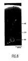
- the lines or viasare formed and they are preferably etched-back or polished to form interconnect lines, as shown in Fig. 5.
- the structureis planarized after the application of the W x Ge y to yield a structure having a conductive via or line, which includes a central, soft, low resistivity metalization 14 having a hard, wear-resistant cap made of W x Ge y or the like.
- the top surface of the via or lineis even with the top surface of the dielectric material on the substrate. Planarization can be accomplished within one or two steps by chemical-mechanical polishing with a slurry such as alumina in dilute ferric nitrate or by RIE in the presence of SF 6 or Cl 2 based chemistry.
- the lines and viascan be formed in one step by depositing the material into vias in combination with GeH 4 reaction and then patterning and etching the lines to form the interconnect structure.
- a low temperature eutectic of Al-Cu-Ge(Cu 3 Ge) can be formed with a GeH 4 reaction at temperatures below 400 °C and furthermore, that a low temperature Ge material containing a hard W cap can be deposited on top of the Al-Cu alloy.
- a processi.e., surface diffusing GeH4 with Al-Cu
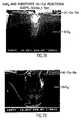
- aspect ratios of 4 to 5are filled without voids as shown in the photographs of Figs. 6 and Figures 7(a) and 7(b).
- the additional experiments performed using GeH 4 reactionsare listed in Table 1 below. The data clearly shows that voids may be filled using the above-described process.
- the above techniqueis advantageous in that it has many applications and the process relies on surface reactions. Hence, it selectively forms a low melting point eutectic alloy in the vias only, thereby to prevent voids and seams.
- the processcan be used as a batch or single wafer reactor (SWR) deposition if desired. Further, the process provides a low-cost technique which can use any PVD technique (e.g., evaporation, standard sputtering, etc.).
- W 3 Ge 5 -20-30 ⁇ Cmhas a polish rate 1/5 of that of pure W. Further, large pads/lines and small pads/lines are protected as well in that resistances of large and small pads remain unchanged.
- the use of low melting-point alloys as via fill materialsis possible. These alloys can be matched with the Al-Cu lines and interconnects so as to prevent electromigration and limited lifetimes. Further, the technique is particularly useful when the lithography ground rules are less than 0.5 micrometer, as in, for example, fabrication of 64Mb and 256Mb dynamic random access memory (DRAM) structures. Additionally, the Al-Cu lines and W can be used for via interconnects between wiring layers.
- a low pressure sputtering processis used along with temperatures below 450 °C.
- the directionalityis improved at low pressure (e.g., below 1.33 x 10 -1 M/m 2 (1 mT), with the preferred range being from 1.07 x 10 -1 N/m 2 (0.2mT to 0.8mT)) although the cosine distribution from the target prevails.
- an aspect ratio of close to 4can be filled without voids (see Table 2).
- the aspect ratiogenerally refers to the ratio of the height of a trench or via relative to its width (in the case of a trench) or its diameter (in the case of a via).
- Trenches and vias with aspect ratios greater than twoare generally considered to have a high aspect ratio.
- the fillis adversely affected as shown in Table 3 below.
- higher aspect ratioe.g., higher than 4
- moderate temperatures below 450 °Care needed.
- the results in Figure 4show that at moderately low pressures and low temperatures, higher aspect ratios (4 and above) can be filled.
- high aspect ratio (aspect ratio of 4 or more) viasmay be filled with a low resistivity metal completely as shown in Tables 2, 3 and 4.
- STEP COVERAGE PRESSURE ASPECT RATIO Al Al-Cu(2%) 2.67 x 10 -2 N/m 2 (0.2 mT) 1.5 100 100 2.0 100 100 3.0 100 98 3.5 100 97 4.0 98 95 POOR FILL AT HIGH PRESSURES ASPECT RATIO PRESSURE Al Al-Cu (2%) 4 5.33 x 10 -2 N/m 2 (0.4 mT) 96 97 1.07 x 10 -1 N/m 2 (0.8 mT) 55 52 2.67 x 10 -1 N/m 2 (2.0 mT) 32 30 GOOD FILL AT LOW PRESSURES AND HIGH TEMPERATURES ASPECT RATIO PRESSURE Al Al-Cu (2%) 4 5.33 x 10 -2 N/m 2 (0.4 mT) 96 97 1.07 x 10 -1 N/m 2 (0.8 mT)
- the two-level structure shown in Figure 8is formed by first depositing sputtered layer (0.8 micrometer) as a stack and then patterning to form a line.
- a dielectric layeras known in the art, was deposited thereon by a deposition/etching/deposition etch process flow. Then, the dielectric was planarized by chemical and mechanical polishing.
- Planarizationcan be accomplished within one or two steps by chemical-mechanical polishing with a slurry such as alumina in dilute ferric nitrate or by RIE in the presence of SF 6 or Cl 2 based chemistry. If chemical-mechanical polishing is employed, slurries can be selected to remove different metal layers on the stack depending on hardnesses of the metal layer.
- viaswere opened up and filled with an Al-Cu stud (having, for example, between 0 to 4 % of Cu) using these two processes (e.g., the GeH 4 reaction with Al-Cu and/or the other process of using sputtering at low pressures and high temperatures).
- the metalwas left in the via by an etchback process employing either chemical and mechanical polishing (using an alumina and ferric nitrate slurry and low polishing pressures) and separately using RIE techniques (using BCl 3 + Cl 2 + CHCl 3 /N 2 ).
- a first level metal line (Ti/Al-Cu (0.5%)/Tiwas formed by forming a trench in a patterned oxide, then polishing the excess metal using softer slurry (e.g., colloidal silica with a low pH compared to alumina and ferric nitrate). Thereafter, an oxide having a thickness of substantially 2 micrometer was deposited thereon. Patterning with metal level 2 (M2) was performed, and then the oxide was etched to 1 micrometer and the resist was removed. Once again, using lithography, the oxide was patterned with vias which were opened down to metal level 1 (M1) with RIE. After removing the resist, metal (e.g., Al-Cu(0.5%)) was sputter deposited at low pressures and at 400 °C. Using the surface diffusion, the high aspect ratios were filled without voids.
- softer slurrye.g., colloidal silica with a low pH compared to alumina and ferric nitrate.
- M2
- a method of creating one of a dual damascene and a damascene structure in combination with reactive ion etching, on a substrate on which a stack including a metal layer (e.g., Al-Cu, Al, Al-Cu-Ge, or the like) having a predetermined hardness, is fabricatedis also provided.
- the methodincludes removing the metal layer having the predetermined hardness, by chemical and mechanical polishing using slurries having a hardness two to three times that of the material to be removed (e.g., colloidal silica in the case of Al-Cu, etc.).
- a hard capsuch as, for example, W x Ge y
- harder suspension particles in the slurrycan be employed (e.g., alumina or the like).
- Electromigration testing of the two level structure(shown in Fig. 9(d)) using a 1.4 ⁇ m-wide and 300 ⁇ m long Al-2%Cu line connected by Al-Cu studs having a 1 ⁇ m diameter was performed at a current density of 1.22 MA/cm 2 at a temperature of 250 °C. The 20% shift in resistance was used as a criterion of failure. The electromigration performance was compared against CVD W studs.
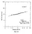
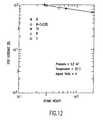
- Figure 12illustrates the relationship of step coverage to atomic weight (or melting point) of the material at room temperature for holes/lines with an aspect ratio of 4.
- Figure 12readily illustrates that with lower atomic weight or melting point material, it is easier to fill the vias at room temperatures and low pressures for aspect ratios below 4.
- other sputtering parametersplay a key role.
- SCK ⁇ M p -a ⁇ M W -a ⁇ P -b ⁇ A R -c ⁇ ⁇ -d ⁇ T e
- step coverage to atomic weight, or the melting point, of the material at room temperature for holes/lines with an aspect ratio of 4is shown and it can clearly be seen that, with lower atomic weight or melting point material, filling of the vias at room temperatures and low pressures for aspect ratios below 4, can be performed more easily.
- the above equationamply illustrates the relationship between step coverages and sputtering parameters for material fill and the fill being dependent on the atomic weight is clearly shown.
- the metallizationincludes a metal alloy for forming at least one of a line and via within a dielectric structure having sidewalls.
- the metal alloyincludes a first element selected from the group consisting of aluminum, gold and silver and a second element of germanium.
- the metal alloyhaving first regions of germanium in a range of from 0 to 40 at. percent and second regions of germanium in the range of from 60 to 100 at. percent.
- the metal alloypreferably includes a third region of Al-Ge and Cu 3 Ge.
- the second region of the metal alloypreferably includes a ternary metal alloy and the metallization preferably includes a layer of W x Ge y over the metal alloy.
- the method described above for forming a metal alloy on a substrate having an upper surfaceincludes heating the upper surface of the substrate to a temperature in the range from 300 to 450°C, and flowing a gas containing germanium over the upper surface of the substrate, the upper surface having regions containing exposed aluminum, or Cu alloys, whereby the germanium in the gas reacts with the Al-Cu to form an aluminum alloy for flowing into adjacent openings due to surface tension of the aluminum alloy.
- the step of flowing a gaspreferably includes selecting GeH 4 .
- the methodalso includes a step of flowing a gas containing W after the step of flowing a gas containing germanium to form a hard cap.
Landscapes
- Engineering & Computer Science (AREA)
- Physics & Mathematics (AREA)
- Condensed Matter Physics & Semiconductors (AREA)
- General Physics & Mathematics (AREA)
- Computer Hardware Design (AREA)
- Microelectronics & Electronic Packaging (AREA)
- Power Engineering (AREA)
- Manufacturing & Machinery (AREA)
- Internal Circuitry In Semiconductor Integrated Circuit Devices (AREA)
- Electrodes Of Semiconductors (AREA)
- Physical Deposition Of Substances That Are Components Of Semiconductor Devices (AREA)
Description
- The present invention generally relates to amethod for fabricating circuits which use field effecttransistors (FETs), bipolar transistors, or BiCMOS (combinedBipolar/Complementary Metal Oxide Silicon structures), andmore particularly to a method forproducing the metallization for interconnecting wiring in anintegrated circuit.
- A WxGeyhard cap is employed for wearresistance.GeH4 gas followed by WF6 can beused to produce the in-situ hard cap of WxGey.
- Low resistivity metals such as aluminum and copper and theirbinary and ternary alloys have been widely explored as fineline interconnects in semiconductor manufacturing. Typicalexamples of fine line interconnect metals include AlxCuy,wherethe sum of x and y is equal to one and both x and y aregreater than or equal to zero and less than or equal to one,ternary alloys such as Al-Pd-Cu and Al-Pd-Nb, Al-Cu-Si, andother similar low resistivity metal-based alloys. Emphasis onscaling down line width dimensions in very large scaleintegrated (VLSI) circuitry manufacture has led to reliabilityproblems including inadequate isolation, electromigration, andplanarization.
- Damascene processes using metal filling vias and linesfollowed by chemical/mechanical polishing (CMP) with variousAl, Cu and Cu-based alloys as are a key element of futurewiring technologies for very large-scale system integration(VLSI). A key problem is filling high aspect ratio vias andlines without voids or seams, and creating homogeneousstructures. Metallo-organic chemical vapor deposition (MOCVD)appears to be a promising method but only in the beginningstages of fabrication, and the deposition rates are very slowand the in-situ deposition of thin lines is very difficult.Additionally, laser melting appears promising but many issuesremain in applying such a fabrication method. Furthermore,high temperature bias sputtering (i.e., above 450 °C)technique has been attempted but this technique haslimitations below 1 µm geometries. Additionally, such hightemperatures would degrade the underlying metals.
- Additionally, conventional techniques such as chemical vapordeposition (CVD) or plating appear promising but as yet havenot been applied to fabrication of such a structure.Currently, there is no method which allows the use of physicalvapor deposition (PVD) techniques or which improves the quality of CVD or plating films if required for filling highaspect ratio vias and lines.
- Further, low resistivity Cu or Al lines are being evaluatedfor back-end metallization and packaging applications.However, good fill of these alloys in submicrometer lines isstill challenging as the existing techniques mentioned abovelack adequate filling properties. The exotic and expensive CVDmethods to deposit Cu or Al-Cu (e.g., metallo-organic chemicalvapor deposition (MOCVD), laser melting, high-temperature biassputtering, Al-Ge on poly substrate, etc.) are being explored,but have drawbacks as mentioned above. Another alternativewould be formation of low eutectic Al-Ge by sputtering, butthis technique requires different targets and a fixedcomposition degrades the lines' electromigration properties.
- Plating is an inexpensive technique, but it cannot deposit anycombination of alloys (e.g., Al-Cu, Al-Nb-Pd, etc).Additionally, pure Cu from Al-Cu alloy is known for its poorcorrosion resistance. Further, any selective technique isprone to loss of selectivity and therefore the capping ofdense Al-Cu lines, without affecting the yield, remains agreat challenge.
- Presently, 4Mb and 16Mb memories typically employ Al-Cu linesand W via interconnects. CVD is used to conformally deposit Winto the vias. However, as dimensions decrease and currentdensities increase, W will have to be replaced with adifferent metal similar to the ones used for the first metallayer (M1) or second metal layer (M2) interconnect structureto form the hard layer. A suitable choice would be Al-Cu orCu. However, these metals are very difficult to deposit byCVD, because of very slow deposition rates, the lack of a goodprecursor, and because deposition occurs at temperatures, suchas above 450 °C, that are believed too high for back-end-of-line(BEOL) applications.
- In one example of the conventional techniques, (as disclosedfor example, in Kikuta et al.PROC. OF 1991 VMIC CONFERENCE,pp.163-170 and Kikuta et al., "0.25 µm Contact Hole Filling byAl-Ge Reflow Sputtering",Proceedings of the 1991 Symposium onVLSI Technology, pp. 35-36), sputtered Al-Ge material was usedfor via fill. However, this structure exhibited high line andvia resistance and also required a polysilicon underlayer.Further, only a binary alloy is described and in a techniquein which alloying is homogeneous, a high Ge content isrequired and thermal stability is degraded.
- It is well-known to deposit low resistivity metals such as Al-Cuby increasing the temperature close to its melting point(e.g., 580 °C) and reflowing it by using substrate biasing.Such high temperatures as well as bias degrades the alreadydeposited metal layers and causes diffusion as well.
Normally, these temperatures in the conventional methods areabove 475 °C. - Other problems of the conventional structures and methods havebeen that damascene of soft metals (e.g., metals such as Al-Cu,Cu, alloys of Al, etc.) shows scratching and smearingusing harder suspension particles in the slurry and thatconventional sputtering techniques are unable to fill linesincluding high temperature, bias sputtering. Significantchallenges exist in filling and forming scratch-free, softmetal lines and the conventional methods have been unable toprovide a practical and effective solution thereto.
- EP-A-0 558 004 discloses creating electrically conductive viasand lines by a three step process. First, a controlled amountof a soft, low resistive metal is deposited in a trench orhole to a point below the top surface of the dielectric inwhich the trench or hole is formed. Subsequently, the lowresistive metal is overcoated with a hard metal such as CVDtungsten. Finally, chemical mechanical polishing is used toplanarize the structure.
- It is therefore an object of the present invention to providea low resistivity line or via with a wear resistant, hard capwhich reduces electromigration.
- The invention provides a method according to
claim 1. As discussed below,GeH4 gas followed by WF6 can beused to produce an in-situ hard cap of WxGey. - A good polish stop is provided in the form of WxGey. The hardcapped WxGey can be formed in one step and, with the invention,there is no degradation of line resistance and theelectromigration of Al-Cu-Ge system can be improved inrelation to the conventional systems.
- The foregoing and other objects, aspects and advantages willbe better understood from the following detailed descriptionof the preferred embodiments of the invention with referenceto the drawings, in which:
- Figures 1(a)-1(b) are cross-sectional views of a semiconductorsubstrate;
- Figures 2(a)-2(b) are cross-sectional views of a semiconductorsubstrate;
- Figures 3(a)-3(b) are cross-sectional views of a semiconductorsubstrate in which voidsencountered during a sputtering process are closed by areaction of GeH4;
- Figure 4 is a cross-sectional view of a semiconductorsubstrate which may be formed by the method of the present invention in which a W-Ge layeris deposited on top as a hard polishing stop;
- Figure 5 is a cross-sectional view of a semiconductorsubstrate in which thelines or vias formed are etched-back or polished to forminterconnect lines.
- Figure 6 is an SEM photograph of the CMP resultant of Al-Cu +GeH4.
- Figure 7(a) and 7(b) are photographs illustrating GeH4 beingreacted to fill aspect ratios close to 4-5.
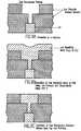
- Figure 8 illustrates a multilevel structure by Example 1.
- Figures 9(a)-9(c) illustrate a dual damascene structureprocess flow and Figure 9(d) illustrates a multilevelstructure produced by Example 2.
- Figure 10 illustrates via chain yield as a function of viaresistance.
- Figure 11(a) illustrates electromigration performance of Al-Custuds/lines by Example 1 and Figure 11(b) illustrateselectromigration performance of Al-Cu studs/lines by Example2.
- Figure 12 is a graph illustrating the relationship of stepcoverage to atomic weight (or melting point) of the materialat room temperature for holes/lines with an aspect ratio of 4.
- Referring now to the drawings, and more particularly to Figure1, there is shown a general process not forming part of thepresent invention. The invention is particularly useful in fabricating circuits using FETs, bipolars, or BiCMOS, and isespecially useful for lithographic structures less than 0.5micrometer , (e.g., those commonly encountered with the 64Mband 256Mb DRAM structures). Of course, the invention is notlimited to such applications and it is envisioned that theinvention could be easily tailored to other applications byone ordinarily skilled in the art reading this application.
- In a process described below but not corresponding to that of the invention low temperaturegermanium gas flow is used to affect metals and alloys deposited inhigh aspect ratio structures including lines and vias. Themetals and alloys preferably include a first element whichpreferably is an element from the group of aluminum, gold andsilver, and a second element of germanium. The metal alloypreferably has first regions of germanium in a range of from 0to 40 at. percent and second regions of germanium in the rangeof from 60 to 100 at. percent. The metal alloy preferablyincludes a third region of Al-Ge and Cu3Ge. The second regionof the metal alloy advantageously includes a ternary metalalloy and the metallization preferably includes a layer ofWxGey over the metal alloy.
- By using a germanium gas flow, Ge will be introduced in asurface reaction that will prevent the appearance of voids andside seams. The surface reaction is also useful in that italso provides a passivating layer of CuGe. Additionally, thegermanium gas flow with WF6 produces a hard cap layer of WxGey.
- More specifically, the method fillshigh aspect ratio lines/vias using surface reactions of GeH4and WF6, in which a low resistivity alloy (e.g., AlxCuy, x + y= 1, 0 < x < 1 ) can be deposited either by chemical vapordeposition (CVD), plating or physical vapor deposition (PVD)techniques.
- The gradual flows of GeH4 at elevated temperatures on thesealloys result in filling up voids or gaps present at the seams or at the sides by forming in-situ low eutectic Al-M-Ge orCu-Ge alloy.
- By slowly introducing WF6, a hard, wear-resistant coating(WxGey) is deposited on top of an Al-Cu-Ge layer as a polishstop for soft alloys. After forming the lines/vias, the Walloy cap can be removed by an SF6 reactive ion etching (RIE)process or the like. The resulting structure formed by thereaction of GeH4 is unique and improves electromigration of thestructure.
- It should be understood that the techniques and resultingstructures are not limited to using any specific substratesand dielectric overlays. Moreover, the invention is notrestricted to any particular metal combinations; rather, anobjective of the invention is to overlay ametal or metal alloy with a W-Ge hard capwhich can withstand wear, corrosion andelectromigration.The invention has particular relevance to electrical systemswhich use aluminum and copper alloys, but can also be equallyused to advantage with other metal alloys.
- A structure andprocess for filling high aspect ratio vias/lines with lowresistivity metal by forming its low melting point eutecticalloy will now be disclosed. Also, the formation of the hardcap of W-Ge as a polishing stop will also be described.
- Generally, as shown in Figures 1-5, first GeH4 is introducedand then WF6 is introduced gradually to form a bilayerstructure of Al-Cu-Ge/WxGey. Here, the GeH4 gas is employed forfilling of the low resistivity alloys deposited practically byany method. For example, any PVD, plating or CVD technique canbe used in combination with GeH4. Examples of such fillingsare shown in Figs. 1-5 and as described below.
- In a first example, as shown in Figures 1(a) and 1(b), asubstrate (not illustrated) is first overcoated with adielectric 10 which is subsequently patterned.
- The substrate is preferably silicon, silicon germanium,germanium, gallium arsenide, or some other material which issuitable for making integrated circuits. However, thesubstrate may be a ceramic, glass, or composite materialcommonly used for packaging semiconductors and for making thinfilm interconnections. The substrate preferably has aplurality of semiconductor devices formed therein which mayinclude field effect transistors (FETs), bipolar transistors,BiCMOS, resistors, Schottky diodes, or the like. Of course,the substrate can have any of the attributes discussed aboveplus many other attributes known within the art.
- The dielectric (a single layer, as shown in the drawings, or acomposite having a plurality of layers) may be formed oforganic and/or inorganic materials. The inorganic materialsmay be silicon dioxide (SiO2), silicon nitride (Si3N4), or thelike. The dielectric 10 is preferably deposited using plasma-enhancedchemical vapor deposition (PECVD). An organicdielectric layer, such as a polyimide or diamond-like carbon(DLC), may be deposited on top or between one or moreinorganic layers of the dielectric.
- Alternative to a dielectric composite created by a pluralityof layers, a single layer of an inorganic dielectric, such asSiO2, PSG, or BPSG, or an organic dielectric, such aspolyimide, may also be employed and may be deposited by any ofa number of well-known techniques such as by growing in anoxidative atmosphere, sputtering, or PECVD. While Figs. 1(a)and 1(b) show the use of a single dielectric layer, it isunderstood that the
dielectric layer 10 is not limitedand that any dielectric (e.g.,inorganic or organic) used by itself or in combination couldbe employed. - An
opening 11 is formed in the dielectric composite, and thisopening may be a via or a trench for a conductive line. InVLSI applications, the substrate is likely to have severalhundred to thousands ofopenings 11 like that shown in Figure1(a) where the resulting dense, complex pattern willultimately interconnect circuits on or in the substrate. Theopenings 11 are preferably formed using contrast-enhancedlithography (CEL) followed by trench or hole etching with amultiwafer tool using CHF3 and O2 with an optimum overetch toensure that the opening 14 has the desired dimensions andextends to a contact on the surface of the substrate for a viastud pattern. - For line patterns, the dielectric layers are preferablypartially etched to a depth about 10% higher than the metalthickness to be employed. When etching polyimide, O2 RIE atlow temperatures is preferred. It should be understood thatthe formation of the
opening 11 is well understood within theart and can be created by many different techniques. - Thereafter, a
suitable material 12 such as Ti followed byAl-Cu or Cu, is deposited by PVD (e.g., evaporated, collimatedsputtering or sputtering without collimation, etc.) in theopenings 11 (e.g., trenches/vias) and over the dielectric 10.Instead of Al, gold or silver can be advantageously used. - Then, a refractory metal layer 13 is deposited on top of theAl-Cu or Cu on the dielectric and in the trenches. Due toshadowing effects, PVD (e.g., evaporation) exhibits seams atthe sides of the structure. Seams are problematic in suchstructures since they pose reliability problems.
- Thereafter, a GeH4 gas is flowed across the top surface of theAl-Cu or
Cu layer 12, and the vias are filled. Preferably, theGeH4 is flowed at a pressure of 1 mT to 760 Torr, and morepreferably 1 Torr, and at a temperature of 300 °C to 450 °C,and more preferably 380 °C to 400 °C. Using GeH4 in combination with Al-Cu lowers the eutectic point of Al-Cu and fills thevias. - As mentioned above, the top of the Al-Cu or Cu is preferablycapped as shown in Fig. 1(a) with the refractory metal. Therefractory metal layer can be titanium (Ti), titanium alloysor compounds such as Ti/TiN, tungsten (W), titanium/tungsten(Ti/W) alloys, or chromium (Cr) or tantalum (Ta) and theiralloys, or some other suitable material. Such a refractorymetal cap prevents the surface reaction from progressing andpromotes the side reaction.
- Preferably, the metalization 14, as shown in Figs. 1(a)-1(b)is AlxCuy, where the sum of x and y is equal to one and both xand y are greater than or equal to zero and less than or equalto one. However, ternary alloys such as Al-Pd-Cu andmulticomponent alloys such as Al-Pd-Nb-Au are also besuitable. The principal characteristic of the metalization 14is that it is a low resistivity and soft material compared tothe refractory metal cap 13.
- Preferably, the
opening 11, which represents the line patternor interlevel via pattern, is filled with the metalization 14to a depth of 100 to 400 nm below the surface of the line orvia. - After reacting this structure with GeH4 as shown in
Equation 1,the side seams are filled with its low melting point eutecticalloy 15 which is Al-Cu-Ge, as shown in Fig. 1(b). - Referring to Figures 2(a)-2(b), thisillustrates the closing of the metal gaps during PVDprocessing (e.g., evaporation, collimation sputtering, etc.)due to the shadowing effects mentioned above.
- Specifically, by reacting the Al-Cu alloy with GeH4 in atemperature range of between 300-450°C and preferably between350 °C to 400 °C, and even more preferably between 380 °C to400 °C, and a pressure range of 26.66 to 133.32 N/m2 (0.2 to1 Torr) in an ultrahigh velocity (UHV) reactor, voids 20 areadvantageously closed, as shown in Fig. 2(b).
- As shown in Figs. 3(a)-3(b), similar voids encountered duringstandard sputtering processes are closed by the reaction of GeH4and the formation of the low melting point eutectic material.Thus, without any complicated technologies, this process can beused for manufacturing to fill vias and lines. The reactionforms the low melting point (m.p.) eutectic alloy and flows thematerial to the center of the void, to thereby fill the void.
- In an alternative process, once the material flow is achieved, a W-
Gelayer 30 or the like is preferably deposited over the refractorymaterial layer and the metalization, as shown in Fig. 4. TheW-Ge layer 30 is advantageously used as a hard, wear-resistantpolishing stop (e.g., it will be more resistant to an aluminaslurry or the like in ferric nitrate used in chemical-mechanicalpolishing or the like). Thereafter, the lines or vias are formedand they are preferably etched-back or polished to forminterconnect lines, as shown in Fig. 5. - The structure is planarized after the application of the WxGey toyield a structure having a conductive via or line, which includesa central, soft, low resistivity metalization 14 having a hard,wear-resistant cap made of WxGey or the like. The top surface ofthe via or line is even with the top surface of the dielectricmaterial on the substrate. Planarization can be accomplishedwithin one or two steps by chemical-mechanical polishing with aslurry such as alumina in dilute ferric nitrate or by RIE in thepresence of SF6 or Cl2 based chemistry.
- Alternatively to the technique described above, the lines andvias can be formed in one step by depositing the material into vias in combination with GeH4 reaction and then patterning andetching the lines to form the interconnect structure.
- Experiments have shown that, with the aforementioned process, a lowtemperature eutectic of Al-Cu-Ge (Cu3Ge) can be formed with aGeH4 reaction at temperatures below 400 °C and furthermore, thata low temperature Ge material containing a hard W cap can bedeposited on top of the Al-Cu alloy. Using such a process (i.e.,surface diffusing GeH4 with Al-Cu) aspect ratios of 4 to 5 arefilled without voids as shown in the photographs of Figs. 6 andFigures 7(a) and 7(b). The additional experiments performedusing GeH4 reactions are listed in Table 1 below. The dataclearly shows that voids may be filled using the above-describedprocess.
Metal Pressure (N/m2(mT)) Step Coverage Aspect Ratio Al-Cu 2.67 x 10⁻² (0.2) 100 % 3.0 6.67 x 10⁻² (0.5) 100 % 2.5 1.07 x 10⁻¹ (0.8) 100 % 2.0 - The above-described technique provides a simple and inexpensivesolution to problems which become worse as the lithographicground rules decrease below 0.5 micrometer.
- Further, the above technique is advantageous in that it has manyapplications and the process relies on surface reactions. Hence,it selectively forms a low melting point eutectic alloy in thevias only, thereby to prevent voids and seams. The processcan be used as a batch or single waferreactor (SWR) deposition if desired. Further, the processprovides a low-cost technique which can use any PVD technique(e.g., evaporation, standard sputtering, etc.).
- Further, regarding the hard cap of WxGey, W3Ge5 -20-30µΩCm has a
polish rate 1/5 of that of pure W. Further, large pads/lines andsmall pads/lines are protected as well in that resistances oflarge and small pads remain unchanged. - Experiments were conducted with the above structure and thefollowing results were found:
Material Holder temperature Resistivity Al-Cu-Ge As-Dep 3.6µΩ Cm 400, 15 min 3.2 µΩ Cm 400, 30 min 4.2 µΩ Cm 400, 40 min 5.9µΩ Cm 400, 60 min 8.9µΩ Cm - In silicon back-end metallization for CMOS as well as bipolarapplications to fill high aspect ratio contacts and vias withconventional techniques in combination with GeH4 and WF6 (if thisis desired) and further the electromigration performance of the Al-Cu alloys using theaforementioned technique and structure can be improved in relation tothat of the conventional structures and methods.
- Further, expensive and complex apparatus are not required, andthe use of low melting-point alloys as via fill materials ispossible. These alloys can be matched with the Al-Cu lines andinterconnects so as to prevent electromigration and limitedlifetimes. Further, the technique is particularly useful whenthe lithography ground rules are less than 0.5 micrometer, as in,for example, fabrication of 64Mb and 256Mb dynamic random accessmemory (DRAM) structures. Additionally, the Al-Cu lines and W canbe used for via interconnects between wiring layers.
- In cases in which high aspect ratio vias/lines are filled bysurface diffusion, a low pressure sputtering process is usedalong with temperatures below 450 °C. Thedirectionality is improved at low pressure (e.g., below 1.33 x 10⁻¹ M/m2 (1mT), with the preferred range being from 1.07 x 10⁻¹ N/m2 (0.2mTto 0.8mT)) although the cosine distribution from the targetprevails. If the deposition is performed at low pressure at roomtemperature (see Table 2 below), an aspect ratio of close to 4can be filled without voids (see Table 2). The aspect ratiogenerally refers to the ratio of the height of a trench or viarelative to its width (in the case of a trench) or its diameter(in the case of a via). Trenches and vias with aspect ratiosgreater than two are generally considered to have a high aspectratio. By increasing the pressure at room temperature, the fillis adversely affected as shown in Table 3 below. Thus, to fillhigher aspect ratio (e.g., higher than 4) moderate temperaturesbelow 450 °C are needed. The results in Figure 4 show that atmoderately low pressures and low temperatures, higher aspectratios (4 and above) can be filled.
- One possible explanation for this behavior may be due to theincrease of kinetic energy of the sputtered atoms emitted at lowpressures. Such atoms with high energy have a low stickingcoefficient (.1 to 0.3) compared to sputtered atoms generated at higher pressure (1.07 x 10⁻¹ N/m2 to 1.33 x 10⁻¹ N/m2 (0.8 mT to 1mT)). Since they have high energy (greater than 1 eV), they donot stick to a vertical wall, but instead bounce off or diffuseuntil a stable configuration is reached. Further, large meanfree paths at lower pressure may assist in minimal collision withother atoms and thus retain the kinetic energy. Additionally,moderate temperatures (e.g., lower than 450 °C) may increase thesurface diffusion characteristics of the sputtered atoms yieldinga void-free fill.
- Thus, at low pressures such as 2.67 x 10⁻² N/m2 (0.2 to 0.8 mT),high aspect ratio (aspect ratio of 4 or more) vias may be filledwith a low resistivity metal completely as shown in Tables 2, 3and 4.
STEP COVERAGE PRESSURE ASPECT RATIO Al Al-Cu (2%) 2.67 x 10⁻² N/m2 (0.2 mT) 1.5 100 100 2.0 100 100 3.0 100 98 3.5 100 97 4.0 98 95 POOR FILL AT HIGH PRESSURES ASPECT RATIO PRESSURE Al Al-Cu (2%) 4 5.33 x 10⁻² N/m2 (0.4 mT) 96 97 1.07 x 10⁻¹ N/m2 (0.8 mT) 55 52 2.67 x 10⁻¹ N/m2 (2.0 mT) 32 30 GOOD FILL AT LOW PRESSURES AND HIGH TEMPERATURES ASPECT RATIO PRESSURE Al Al-Cu (2%) 4 5.33 x 10⁻² N/m2 (0.4 mT) 100 100 1.07 x 10⁻¹ N/m2 (0.8 mT) 100 100 2.67 x 10⁻¹ N/m2 (2.0 mT) 80 70 - The two-level structure shown in Figure 8 is formed by firstdepositing sputtered layer (0.8 micrometer) as a stack and thenpatterning to form a line. A dielectric layer, as known in theart, was deposited thereon by a deposition/etching/depositionetch process flow. Then, the dielectric was planarized bychemical and mechanical polishing.
- Planarization can be accomplished within one or two steps bychemical-mechanical polishing with a slurry such as alumina indilute ferric nitrate or by RIE in the presence of SF6 or Cl2based chemistry. If chemical-mechanical polishing is employed,slurries can be selected to remove different metal layers on thestack depending on hardnesses of the metal layer.
- Thereafter, vias were opened up and filled with an Al-Cu stud(having, for example, between 0 to 4 % of Cu) using these twoprocesses (e.g., the GeH4 reaction with Al-Cu and/or the otherprocess of using sputtering at low pressures and hightemperatures). The metal was left in the via by an etchbackprocess employing either chemical and mechanical polishing (usingan alumina and ferric nitrate slurry and low polishing pressures)and separately using RIE techniques (using BCl3 + Cl2 + CHCl3/N2).
- If chemical and mechanical polishing is employed, slurries canbe selected to provide scratch-free surfaces. Once again, theTi/Al-Cu/Ti/TiN layer was deposited on top of these vias and thenpatterned by lithography and formed by RIE to form aninterconnect. Such a structure has been electrically tested bythe present inventors.
- In a further example, as shown in Figs . 9 (a)-9(d),a first level metal line (Ti/Al-Cu (0.5%)/Ti was formed byforming a trench in a patterned oxide, then polishing the excessmetal using softer slurry (e.g., colloidal silica with a low pHcompared to alumina and ferric nitrate). Thereafter, an oxidehaving a thickness of substantially 2 micrometer was depositedthereon. Patterning with metal level 2 (M2) was performed, andthen the oxide was etched to 1 micrometer and the resist wasremoved. Once again, using lithography, the oxide was patternedwith vias which were opened down to metal level 1 (M1) with RIE.After removing the resist, metal (e.g., Al-Cu(0.5%)) was sputterdeposited at low pressures and at 400 °C. Using the surfacediffusion, the high aspect ratios were filled without voids.
- Using the above-mentioned polishing process, Al-Cu was removedfrom the field oxide and thus a dual damascene structure wascreated, as shown in Figure 9(d).
- Thus, a method of creating one of adual damascene and a damascene structure in combination withreactive ion etching, on a substrate on which a stack includinga metal layer (e.g., Al-Cu, Al, Al-Cu-Ge, or the like) having apredetermined hardness, is fabricated, is also provided. Themethod includes removing the metal layer having the predeterminedhardness, by chemical and mechanical polishing using slurrieshaving a hardness two to three times that of the material to beremoved (e.g., colloidal silica in the case of Al-Cu, etc.).Furthermore, if a hard cap such as, for example, WxGey, isemployed, then harder suspension particles in the slurry can beemployed (e.g., alumina or the like).
- Electrical Results were obtained via chain resistance of theobtained multilevel structure using these different examplesas shown in Figure 10. The distribution isnormal with a mean resistance of 0.5kΩ Ohms for a chain (500vias/chain, via size of 0.7 µm, and 38 chains tested). The yieldon the chain is 100%. The via resistance is comparable to CVDW studs.
- Electromigration testing of the two level structure (shown inFig. 9(d)) using a 1.4 µm-wide and 300 µm long Al-2%Cu lineconnected by Al-Cu studs having a 1 µm diameter was performed ata current density of 1.22 MA/cm2 at a temperature of 250 °C. The20% shift in resistance was used as a criterion of failure. Theelectromigration performance was compared against CVD W studs.
- An electromigration normal logarithmic plot for Al-Cu formed GeH4reaction and Al-Cu alone by low pressure sputtering at 440 °Calone is shown in Figs. 11(a) and 11(b), respectively. W viasamples (not illustrated) shift to higher resistance values thanAl-Cu via samples before electrical opening (i.e., completefailure). A 20% change in the resistance as the failurecriterion, the Al-Cu via sample exhibits a higher mean-time-to-failt50 (for Al-Cu-Ge sample: 116 hours, and for low pressure440 °C sputtered Al-Cu: 6161 hours as opposed to 86 hours for CVDW) and a higher σ than the W via samples compared with them.Hence, the Al-Cu via electromigration results show significantimprovement in t50 over CVD W via samples.
- As pointed out above, several factors affect the fill for lowresistivity metal including pressure and temperature which thepresent inventors have studied to explore the surface diffusioneffects.
- Figure 12 illustrates the relationship of step coverage to atomicweight (or melting point) of the material at room temperature forholes/lines with an aspect ratio of 4. Figure 12 readilyillustrates that with lower atomic weight or melting pointmaterial, it is easier to fill the vias at room temperatures andlow pressures for aspect ratios below 4. To fill higher aspectratios, other sputtering parameters play a key role. To achievesuch material fill, a relationship between step coverages andsputtering parameters for material fill has been found by thepresent inventors. The relationship is as shown in
Equation 2. - In
Equation 2,
SC is the step coverage of the material to be filled;
Mp is the melting point of the material;
MW is the atomic weight of the material;
AR is the aspect ratio of the trench or hole;
P is the operating pressure (mT);
T is the substrate temperature (°C);
is a dimensionless quantity = tan() = D1-D2/2H; and
K = material dependent constant.
Constants and coefficients are as follows:
a = 0.2b = 0.25 (high weight) - 0.51 (low weight)
c = 0.21 - 0.27
≤ 0.03 (for low weight) (e.g. Al, Al-Cu)
d ≤ 0.1
e = 0.6 - 0.7
K = 3-5 (≈ 4.0 - 4.5)
D1 = diameter of target
D2 = diameter of substrate
H = distance between target and substrate - Hence, as illustrated in Figure 12, the relationship of stepcoverage to atomic weight, or the melting point, of the materialat room temperature for holes/lines with an aspect ratio of 4 isshown and it can clearly be seen that, with lower atomic weightor melting point material, filling of the vias at roomtemperatures and low pressures for aspect ratios below 4, can beperformed more easily. Further, the above equation amplyillustrates the relationship between step coverages andsputtering parameters for material fill and the fill beingdependent on the atomic weight is clearly shown.
- Thus, as described above, ametallization for interconnecting wiring in anintegrated circuit is provided. The metallization includes a metal alloy forforming at least one of a line and via within a dielectricstructure having sidewalls. The metal alloy includes a firstelement selected from the group consisting of aluminum, gold and silver and a second element of germanium. The metal alloy havingfirst regions of germanium in a range of from 0 to 40 at. percentand second regions of germanium in the range of from 60 to 100at. percent. The metal alloy preferably includes a third regionof Al-Ge and Cu3Ge. The second region of the metal alloypreferably includes a ternary metal alloy and the metallizationpreferably includes a layer of WxGey over the metal alloy.
- Further, the method described above for forming a metal alloy on asubstrate having an upper surface, includes heating the uppersurface of the substrate to a temperature in the range from 300to 450°C, and flowing a gas containing germanium over the uppersurface of the substrate, the upper surface having regionscontaining exposed aluminum, or Cu alloys, whereby the germaniumin the gas reacts with the Al-Cu to form an aluminum alloy forflowing into adjacent openings due to surface tension of the aluminumalloy. The step of flowing a gas preferably includesselecting GeH4. Preferably, the method also includes a step offlowing a gas containing W after the step of flowing a gascontaining germanium to form a hard cap.
Claims (2)
- A method of creating one of a dual damascene and adamascene structure on a substrate on which a stack isfabricated, said stack including a metal layer having ahardness, said method comprising the steps of:characterized in thatremoving said metal layer having said hardness, bychemical and mechanical polishing using slurries having ahardness at least twice that of said metal layer to beremoved,said step of removing including chemical and mechanicalpolishing employing a slurry including alumina;
said metal layer has a hard cap consisting of a tungsten-germaniumalloy functioning as a chemical mechanicalpolishing stop layer. - A method according to claim 1, wherein said slurryhardness is two to three times as hard as saidmetal layer to be removed.
Applications Claiming Priority (3)
| Application Number | Priority Date | Filing Date | Title |
|---|---|---|---|
| US28660594A | 1994-08-05 | 1994-08-05 | |
| US286605 | 1994-08-05 | ||
| EP95110478AEP0697730B1 (en) | 1994-08-05 | 1995-07-05 | Method of forming an Al-Ge alloy with WGe polishing stop |
Related Parent Applications (1)
| Application Number | Title | Priority Date | Filing Date |
|---|---|---|---|
| EP95110478ADivisionEP0697730B1 (en) | 1994-08-05 | 1995-07-05 | Method of forming an Al-Ge alloy with WGe polishing stop |
Publications (2)
| Publication Number | Publication Date |
|---|---|
| EP0915501A1 EP0915501A1 (en) | 1999-05-12 |
| EP0915501B1true EP0915501B1 (en) | 2003-02-26 |
Family
ID=23099349
Family Applications (2)
| Application Number | Title | Priority Date | Filing Date |
|---|---|---|---|
| EP95110478AExpired - LifetimeEP0697730B1 (en) | 1994-08-05 | 1995-07-05 | Method of forming an Al-Ge alloy with WGe polishing stop |
| EP99101825AExpired - LifetimeEP0915501B1 (en) | 1994-08-05 | 1995-07-05 | Method of forming a damascene structure with WGe polishing stop |
Family Applications Before (1)
| Application Number | Title | Priority Date | Filing Date |
|---|---|---|---|
| EP95110478AExpired - LifetimeEP0697730B1 (en) | 1994-08-05 | 1995-07-05 | Method of forming an Al-Ge alloy with WGe polishing stop |
Country Status (6)
| Country | Link |
|---|---|
| US (4) | US5856026A (en) |
| EP (2) | EP0697730B1 (en) |
| JP (1) | JP3083735B2 (en) |
| KR (1) | KR0177537B1 (en) |
| DE (2) | DE69529775T2 (en) |
| TW (1) | TW344101B (en) |
Families Citing this family (92)
| Publication number | Priority date | Publication date | Assignee | Title |
|---|---|---|---|---|
| SI0669114T1 (en)* | 1994-02-25 | 1999-02-28 | Robert E. Fischell | Stent having a multiplicity of closed circular structures |
| EP0697730B1 (en)* | 1994-08-05 | 1999-11-24 | International Business Machines Corporation | Method of forming an Al-Ge alloy with WGe polishing stop |
| US5789317A (en)* | 1996-04-12 | 1998-08-04 | Micron Technology, Inc. | Low temperature reflow method for filling high aspect ratio contacts |
| US6429120B1 (en)* | 2000-01-18 | 2002-08-06 | Micron Technology, Inc. | Methods and apparatus for making integrated-circuit wiring from copper, silver, gold, and other metals |
| US6309971B1 (en) | 1996-08-01 | 2001-10-30 | Cypress Semiconductor Corporation | Hot metallization process |
| US5916453A (en)* | 1996-09-20 | 1999-06-29 | Fujitsu Limited | Methods of planarizing structures on wafers and substrates by polishing |
| JP3583562B2 (en) | 1996-10-18 | 2004-11-04 | 株式会社東芝 | Semiconductor device |
| KR100221656B1 (en)* | 1996-10-23 | 1999-09-15 | 구본준 | Wiring forming method |
| US6171957B1 (en)* | 1997-07-16 | 2001-01-09 | Mitsubishi Denki Kabushiki Kaisha | Manufacturing method of semiconductor device having high pressure reflow process |
| US6100184A (en)* | 1997-08-20 | 2000-08-08 | Sematech, Inc. | Method of making a dual damascene interconnect structure using low dielectric constant material for an inter-level dielectric layer |
| US6140228A (en)* | 1997-11-13 | 2000-10-31 | Cypress Semiconductor Corporation | Low temperature metallization process |
| US6211073B1 (en) | 1998-02-27 | 2001-04-03 | Micron Technology, Inc. | Methods for making copper and other metal interconnections in integrated circuits |
| US6015749A (en)* | 1998-05-04 | 2000-01-18 | Taiwan Semiconductor Manufacturing Company | Method to improve adhesion between copper and titanium nitride, for copper interconnect structures, via the use of an ion implantation procedure |
| US6362097B1 (en)* | 1998-07-14 | 2002-03-26 | Applied Komatsu Technlology, Inc. | Collimated sputtering of semiconductor and other films |
| KR100265772B1 (en)* | 1998-07-22 | 2000-10-02 | 윤종용 | Wiring structure of semicondcutor device and manufacturing method thereof |
| US6287977B1 (en) | 1998-07-31 | 2001-09-11 | Applied Materials, Inc. | Method and apparatus for forming improved metal interconnects |
| US6284656B1 (en) | 1998-08-04 | 2001-09-04 | Micron Technology, Inc. | Copper metallurgy in integrated circuits |
| US6288442B1 (en) | 1998-09-10 | 2001-09-11 | Micron Technology, Inc. | Integrated circuit with oxidation-resistant polymeric layer |
| US6004188A (en)* | 1998-09-10 | 1999-12-21 | Chartered Semiconductor Manufacturing Ltd. | Method for forming copper damascene structures by using a dual CMP barrier layer |
| US6051496A (en)* | 1998-09-17 | 2000-04-18 | Taiwan Semiconductor Manufacturing Company | Use of stop layer for chemical mechanical polishing of CU damascene |
| US6180480B1 (en) | 1998-09-28 | 2001-01-30 | International Business Machines Corporation | Germanium or silicon-germanium deep trench fill by melt-flow process |
| US6069082A (en)* | 1998-10-13 | 2000-05-30 | Chartered Semiconductor Manufacturing Ltd. | Method to prevent dishing in damascene CMP process |
| US6274253B1 (en)* | 1998-11-13 | 2001-08-14 | Micron Technology, Inc. | Processing methods for providing metal-comprising materials within high aspect ratio openings |
| US6143657A (en)* | 1999-01-04 | 2000-11-07 | Taiwan Semiconductor Manufacturing Company | Method of increasing the stability of a copper to copper interconnection process and structure manufactured thereby |
| US6130162A (en)* | 1999-01-04 | 2000-10-10 | Taiwan Semiconductor Manufacturing Company | Method of preparing passivated copper line and device manufactured thereby |
| US6174799B1 (en)* | 1999-01-05 | 2001-01-16 | Advanced Micro Devices, Inc. | Graded compound seed layers for semiconductors |
| US6114246A (en)* | 1999-01-07 | 2000-09-05 | Vlsi Technology, Inc. | Method of using a polish stop film to control dishing during copper chemical mechanical polishing |
| US20020127845A1 (en)* | 1999-03-01 | 2002-09-12 | Paul A. Farrar | Conductive structures in integrated circuits |
| US6281127B1 (en) | 1999-04-15 | 2001-08-28 | Taiwan Semiconductor Manufacturing Company | Self-passivation procedure for a copper damascene structure |
| US6194307B1 (en) | 1999-04-26 | 2001-02-27 | Taiwan Semiconductor Manufacturing Company | Elimination of copper line damages for damascene process |
| US6071808A (en)* | 1999-06-23 | 2000-06-06 | Lucent Technologies Inc. | Method of passivating copper interconnects in a semiconductor |
| US6046108A (en)* | 1999-06-25 | 2000-04-04 | Taiwan Semiconductor Manufacturing Company | Method for selective growth of Cu3 Ge or Cu5 Si for passivation of damascene copper structures and device manufactured thereby |
| US6387810B2 (en)* | 1999-06-28 | 2002-05-14 | International Business Machines Corporation | Method for homogenizing device parameters through photoresist planarization |
| US6248665B1 (en) | 1999-07-06 | 2001-06-19 | Taiwan Semiconductor Manufacturing Company | Delamination improvement between Cu and dielectrics for damascene process |
| US6391780B1 (en) | 1999-08-23 | 2002-05-21 | Taiwan Semiconductor Manufacturing Company | Method to prevent copper CMP dishing |
| US6248002B1 (en) | 1999-10-20 | 2001-06-19 | Taiwan Semiconductor Manufacturing Company | Obtaining the better defect performance of the fuse CMP process by adding slurry polish on more soft pad after slurry polish |
| US6114243A (en)* | 1999-11-15 | 2000-09-05 | Chartered Semiconductor Manufacturing Ltd | Method to avoid copper contamination on the sidewall of a via or a dual damascene structure |
| US6344419B1 (en) | 1999-12-03 | 2002-02-05 | Applied Materials, Inc. | Pulsed-mode RF bias for sidewall coverage improvement |
| US6627541B1 (en)* | 1999-12-15 | 2003-09-30 | Texas Instruments Incorporated | Reflow method for construction of conductive vias |
| US6361880B1 (en) | 1999-12-22 | 2002-03-26 | International Business Machines Corporation | CVD/PVD/CVD/PVD fill process |
| US6969448B1 (en) | 1999-12-30 | 2005-11-29 | Cypress Semiconductor Corp. | Method for forming a metallization structure in an integrated circuit |
| US6455427B1 (en) | 1999-12-30 | 2002-09-24 | Cypress Semiconductor Corp. | Method for forming void-free metallization in an integrated circuit |
| US6376370B1 (en) | 2000-01-18 | 2002-04-23 | Micron Technology, Inc. | Process for providing seed layers for using aluminum, copper, gold and silver metallurgy process for providing seed layers for using aluminum, copper, gold and silver metallurgy |
| US6420262B1 (en) | 2000-01-18 | 2002-07-16 | Micron Technology, Inc. | Structures and methods to enhance copper metallization |
| US7262130B1 (en)* | 2000-01-18 | 2007-08-28 | Micron Technology, Inc. | Methods for making integrated-circuit wiring from copper, silver, gold, and other metals |
| US7211512B1 (en)* | 2000-01-18 | 2007-05-01 | Micron Technology, Inc. | Selective electroless-plated copper metallization |
| US6339029B1 (en) | 2000-01-19 | 2002-01-15 | Taiwan Semiconductor Manufacturing Company | Method to form copper interconnects |
| US6329290B1 (en)* | 2000-02-24 | 2001-12-11 | Conexant Systems, Inc. | Method for fabrication and structure for high aspect ratio vias |
| US6674167B1 (en)* | 2000-05-31 | 2004-01-06 | Micron Technology, Inc. | Multilevel copper interconnect with double passivation |
| US6335261B1 (en) | 2000-05-31 | 2002-01-01 | International Business Machines Corporation | Directional CVD process with optimized etchback |
| US6423629B1 (en) | 2000-05-31 | 2002-07-23 | Kie Y. Ahn | Multilevel copper interconnects with low-k dielectrics and air gaps |
| US6554979B2 (en) | 2000-06-05 | 2003-04-29 | Applied Materials, Inc. | Method and apparatus for bias deposition in a modulating electric field |
| DE10032792A1 (en)* | 2000-06-28 | 2002-01-17 | Infineon Technologies Ag | Method of making via hole wiring |
| US6429118B1 (en) | 2000-09-18 | 2002-08-06 | Taiwan Semiconductor Manufacturing Company | Elimination of electrochemical deposition copper line damage for damascene processing |
| US6383935B1 (en) | 2000-10-16 | 2002-05-07 | Taiwan Semiconductor Manufacturing Company | Method of reducing dishing and erosion using a sacrificial layer |
| US6433402B1 (en)* | 2000-11-16 | 2002-08-13 | Advanced Micro Devices, Inc. | Selective copper alloy deposition |
| US7067440B1 (en) | 2001-08-24 | 2006-06-27 | Novellus Systems, Inc. | Gap fill for high aspect ratio structures |
| US6746591B2 (en) | 2001-10-16 | 2004-06-08 | Applied Materials Inc. | ECP gap fill by modulating the voltate on the seed layer to increase copper concentration inside feature |
| US6794290B1 (en) | 2001-12-03 | 2004-09-21 | Novellus Systems, Inc. | Method of chemical modification of structure topography |
| US7138719B2 (en)* | 2002-08-29 | 2006-11-21 | Micron Technology, Inc. | Trench interconnect structure and formation method |
| US7122485B1 (en) | 2002-12-09 | 2006-10-17 | Novellus Systems, Inc. | Deposition profile modification through process chemistry |
| US7220665B2 (en) | 2003-08-05 | 2007-05-22 | Micron Technology, Inc. | H2 plasma treatment |
| US7078312B1 (en) | 2003-09-02 | 2006-07-18 | Novellus Systems, Inc. | Method for controlling etch process repeatability |
| US7344996B1 (en) | 2005-06-22 | 2008-03-18 | Novellus Systems, Inc. | Helium-based etch process in deposition-etch-deposition gap fill |
| US7163896B1 (en) | 2003-12-10 | 2007-01-16 | Novellus Systems, Inc. | Biased H2 etch process in deposition-etch-deposition gap fill |
| US7476621B1 (en) | 2003-12-10 | 2009-01-13 | Novellus Systems, Inc. | Halogen-free noble gas assisted H2 plasma etch process in deposition-etch-deposition gap fill |
| US7199045B2 (en)* | 2004-05-26 | 2007-04-03 | Taiwan Semiconductor Manufacturing Company, Ltd. | Metal-filled openings for submicron devices and methods of manufacture thereof |
| US7217658B1 (en) | 2004-09-07 | 2007-05-15 | Novellus Systems, Inc. | Process modulation to prevent structure erosion during gap fill |
| US7176039B1 (en) | 2004-09-21 | 2007-02-13 | Novellus Systems, Inc. | Dynamic modification of gap fill process characteristics |
| US7381451B1 (en) | 2004-11-17 | 2008-06-03 | Novellus Systems, Inc. | Strain engineering—HDP thin film with tensile stress for FEOL and other applications |
| US7211525B1 (en) | 2005-03-16 | 2007-05-01 | Novellus Systems, Inc. | Hydrogen treatment enhanced gap fill |
| US20070052107A1 (en)* | 2005-09-05 | 2007-03-08 | Cheng-Ming Weng | Multi-layered structure and fabricating method thereof and dual damascene structure, interconnect structure and capacitor |
| US7563714B2 (en)* | 2006-01-13 | 2009-07-21 | International Business Machines Corporation | Low resistance and inductance backside through vias and methods of fabricating same |
| US7491643B2 (en)* | 2006-05-24 | 2009-02-17 | International Business Machines Corporation | Method and structure for reducing contact resistance between silicide contact and overlying metallization |
| US7482245B1 (en) | 2006-06-20 | 2009-01-27 | Novellus Systems, Inc. | Stress profile modulation in STI gap fill |
| US7648921B2 (en)* | 2006-09-22 | 2010-01-19 | Macronix International Co., Ltd. | Method of forming dielectric layer |
| US7666781B2 (en)* | 2006-11-22 | 2010-02-23 | International Business Machines Corporation | Interconnect structures with improved electromigration resistance and methods for forming such interconnect structures |
| US7629212B2 (en)* | 2007-03-19 | 2009-12-08 | Texas Instruments Incorporated | Doped WGe to form dual metal gates |
| US7651939B2 (en) | 2007-05-01 | 2010-01-26 | Freescale Semiconductor, Inc | Method of blocking a void during contact formation |
| US7994034B2 (en)* | 2008-03-10 | 2011-08-09 | Ovonyx, Inc. | Temperature and pressure control methods to fill features with programmable resistance and switching devices |
| KR100905872B1 (en)* | 2007-08-24 | 2009-07-03 | 주식회사 하이닉스반도체 | Metal wiring formation method of semiconductor device |
| US8133797B2 (en)* | 2008-05-16 | 2012-03-13 | Novellus Systems, Inc. | Protective layer to enable damage free gap fill |
| KR20120124634A (en)* | 2011-05-04 | 2012-11-14 | 삼성전자주식회사 | Method of manufacturing a semiconductor device and method of manufacturing a semiconductor package including the same |
| US8697562B2 (en) | 2011-06-23 | 2014-04-15 | Richard L. McCreery | Metal contacts for molecular device junctions and surface-diffusion-mediated deposition |
| US8575000B2 (en)* | 2011-07-19 | 2013-11-05 | SanDisk Technologies, Inc. | Copper interconnects separated by air gaps and method of making thereof |
| KR20140124386A (en)* | 2012-02-13 | 2014-10-24 | 어플라이드 머티어리얼스, 인코포레이티드 | Selective epitaxial germanium growth on silicon-trench fill and in situ doping |
| US9997458B2 (en) | 2012-05-14 | 2018-06-12 | Imec Vzw | Method for manufacturing germamde interconnect structures and corresponding interconnect structures |
| KR20220031134A (en) | 2014-06-16 | 2022-03-11 | 인텔 코포레이션 | Seam healing of metal interconnects |
| US9953940B2 (en) | 2015-06-26 | 2018-04-24 | International Business Machines Corporation | Corrosion resistant aluminum bond pad structure |
| US10692986B2 (en)* | 2016-06-17 | 2020-06-23 | National Institute Of Advanced Industrial Science And Technology | Compound film of tungsten and germanium, and semiconductor device |
| US11183443B2 (en)* | 2019-06-13 | 2021-11-23 | Nanya Technology Corporation | Semiconductor structure and method for manufacturing the same |
| US20240339400A1 (en)* | 2023-04-10 | 2024-10-10 | Nanya Technology Corporation | Semiconductor device with filling layer and method for fabricating the same |
Family Cites Families (28)
| Publication number | Priority date | Publication date | Assignee | Title |
|---|---|---|---|---|
| NL278654A (en)* | 1961-06-08 | |||
| US3222630A (en)* | 1961-06-26 | 1965-12-07 | Texas Instruments Inc | Aluminum-germanium contact |
| US3501829A (en)* | 1966-07-18 | 1970-03-24 | United Aircraft Corp | Method of applying contacts to a microcircuit |
| US4022625A (en)* | 1974-12-24 | 1977-05-10 | Nl Industries, Inc. | Polishing composition and method of polishing |
| US4188710A (en)* | 1978-08-11 | 1980-02-19 | The United States Of America As Represented By The Secretary Of The Navy | Ohmic contacts for group III-V n-type semiconductors using epitaxial germanium films |
| US4207546A (en)* | 1978-12-07 | 1980-06-10 | United Technologies Corporation | Phase and amplitude programmable internal mixing SAW signal processor |
| US4301188A (en)* | 1979-10-01 | 1981-11-17 | Bell Telephone Laboratories, Incorporated | Process for producing contact to GaAs active region |
| US4321099A (en)* | 1979-11-13 | 1982-03-23 | Nasa | Method of fabricating Schottky barrier solar cell |
| JPH01107558A (en)* | 1987-10-20 | 1989-04-25 | Matsushita Electric Ind Co Ltd | Manufacture of thin metal film wiring |
| US5121174A (en)* | 1987-10-23 | 1992-06-09 | Vitesse Semiconductor Corporation | Gate-to-ohmic metal contact scheme for III-V devices |
| DE68927116T2 (en)* | 1988-01-19 | 1997-02-06 | Fujimi Inc | Polishing compound |
| US4908182A (en)* | 1988-04-11 | 1990-03-13 | Polytechnic University | Rapidly solidified high strength, ductile dispersion-hardened tungsten-rich alloys |
| JPH02257640A (en)* | 1989-03-30 | 1990-10-18 | Oki Electric Ind Co Ltd | Manufacture of semiconductor element |
| JPH03122273A (en)* | 1989-10-06 | 1991-05-24 | Hitachi Ltd | Film deposition equipment using microwaves |
| KR960001601B1 (en)* | 1992-01-23 | 1996-02-02 | 삼성전자주식회사 | Contact hole embedding method and structure of semiconductor device |
| JP2841976B2 (en)* | 1990-11-28 | 1998-12-24 | 日本電気株式会社 | Semiconductor device and manufacturing method thereof |
| US5143867A (en)* | 1991-02-13 | 1992-09-01 | International Business Machines Corporation | Method for depositing interconnection metallurgy using low temperature alloy processes |
| JPH04334019A (en)* | 1991-05-09 | 1992-11-20 | Hitachi Ltd | Manufacture of compound semiconductor device |
| US5171412A (en)* | 1991-08-23 | 1992-12-15 | Applied Materials, Inc. | Material deposition method for integrated circuit manufacturing |
| US5262354A (en)* | 1992-02-26 | 1993-11-16 | International Business Machines Corporation | Refractory metal capped low resistivity metal conductor lines and vias |
| US5300813A (en)* | 1992-02-26 | 1994-04-05 | International Business Machines Corporation | Refractory metal capped low resistivity metal conductor lines and vias |
| JP2547935B2 (en)* | 1992-04-30 | 1996-10-30 | インターナショナル・ビジネス・マシーンズ・コーポレイション | Method for forming interconnection structure of semiconductor integrated circuit |
| US5314840A (en)* | 1992-12-18 | 1994-05-24 | International Business Machines Corporation | Method for forming an antifuse element with electrical or optical programming |
| US5356513A (en)* | 1993-04-22 | 1994-10-18 | International Business Machines Corporation | Polishstop planarization method and structure |
| US5300130A (en)* | 1993-07-26 | 1994-04-05 | Saint Gobain/Norton Industrial Ceramics Corp. | Polishing material |
| US5332467A (en)* | 1993-09-20 | 1994-07-26 | Industrial Technology Research Institute | Chemical/mechanical polishing for ULSI planarization |
| EP0697730B1 (en)* | 1994-08-05 | 1999-11-24 | International Business Machines Corporation | Method of forming an Al-Ge alloy with WGe polishing stop |
| US5527423A (en)* | 1994-10-06 | 1996-06-18 | Cabot Corporation | Chemical mechanical polishing slurry for metal layers |
- 1995
- 1995-07-05EPEP95110478Apatent/EP0697730B1/ennot_activeExpired - Lifetime
- 1995-07-05EPEP99101825Apatent/EP0915501B1/ennot_activeExpired - Lifetime
- 1995-07-05DEDE69529775Tpatent/DE69529775T2/ennot_activeExpired - Lifetime
- 1995-07-05DEDE69513459Tpatent/DE69513459T2/ennot_activeExpired - Lifetime
- 1995-08-01JPJP07196745Apatent/JP3083735B2/ennot_activeExpired - Fee Related
- 1995-08-04KRKR1019950024042Apatent/KR0177537B1/ennot_activeExpired - Fee Related
- 1995-08-11TWTW084108376Apatent/TW344101B/ennot_activeIP Right Cessation
- 1996
- 1996-02-20USUS08/603,092patent/US5856026A/ennot_activeExpired - Fee Related
- 1996-10-28USUS08/738,901patent/US5731245A/ennot_activeExpired - Fee Related
- 1996-10-28USUS08/738,883patent/US5897370A/ennot_activeExpired - Lifetime
- 1997
- 1997-09-30USUS08/941,062patent/US5877084A/ennot_activeExpired - Fee Related
Also Published As
| Publication number | Publication date |
|---|---|
| US5897370A (en) | 1999-04-27 |
| KR0177537B1 (en) | 1999-04-15 |
| JPH0864599A (en) | 1996-03-08 |
| EP0697730A2 (en) | 1996-02-21 |
| US5731245A (en) | 1998-03-24 |
| EP0697730A3 (en) | 1996-08-14 |
| TW344101B (en) | 1998-11-01 |
| DE69529775D1 (en) | 2003-04-03 |
| EP0697730B1 (en) | 1999-11-24 |
| DE69529775T2 (en) | 2003-10-16 |
| US5877084A (en) | 1999-03-02 |
| EP0915501A1 (en) | 1999-05-12 |
| US5856026A (en) | 1999-01-05 |
| DE69513459D1 (en) | 1999-12-30 |
| DE69513459T2 (en) | 2000-10-26 |
| JP3083735B2 (en) | 2000-09-04 |
| KR960009109A (en) | 1996-03-22 |
Similar Documents
| Publication | Publication Date | Title |
|---|---|---|
| EP0915501B1 (en) | Method of forming a damascene structure with WGe polishing stop | |
| US6323554B1 (en) | Refractory metal capped low resistivity metal conductor lines and vias formed using PVD and CVD | |
| US5925933A (en) | Interconnect structure using Al2 -Cu for an integrated circuit chip | |
| US5262354A (en) | Refractory metal capped low resistivity metal conductor lines and vias | |
| US7679193B2 (en) | Use of AIN as cooper passivation layer and thermal conductor | |
| US5472912A (en) | Method of making an integrated circuit structure by using a non-conductive plug | |
| EP0430403B1 (en) | Method for fabricating interlevel contacts | |
| US6576543B2 (en) | Method for selectively depositing diffusion barriers | |
| US6215189B1 (en) | Semiconductor device having interconnect layer and method of manufacturing therefor | |
| EP0833381B1 (en) | Method of forming electrical connections for a semiconductor | |
| US6242811B1 (en) | Interlevel contact including aluminum-refractory metal alloy formed during aluminum deposition at an elevated temperature | |
| HK1001601B (en) | Refractory metal capped low resistivity metal conductor lines and vias |
Legal Events
| Date | Code | Title | Description |
|---|---|---|---|
| PUAI | Public reference made under article 153(3) epc to a published international application that has entered the european phase | Free format text:ORIGINAL CODE: 0009012 | |
| 17P | Request for examination filed | Effective date:19990128 | |
| AC | Divisional application: reference to earlier application | Ref document number:697730 Country of ref document:EP | |
| AK | Designated contracting states | Kind code of ref document:A1 Designated state(s):DE FR GB | |
| 17Q | First examination report despatched | Effective date:20020215 | |
| GRAG | Despatch of communication of intention to grant | Free format text:ORIGINAL CODE: EPIDOS AGRA | |
| RTI1 | Title (correction) | Free format text:METHOD OF FORMING A DAMASCENE STRUCTURE WITH WGE POLISHING STOP | |
| GRAG | Despatch of communication of intention to grant | Free format text:ORIGINAL CODE: EPIDOS AGRA | |
| GRAH | Despatch of communication of intention to grant a patent | Free format text:ORIGINAL CODE: EPIDOS IGRA | |
| GRAA | (expected) grant | Free format text:ORIGINAL CODE: 0009210 | |
| AC | Divisional application: reference to earlier application | Ref document number:0697730 Country of ref document:EP Kind code of ref document:P | |
| AK | Designated contracting states | Designated state(s):DE FR GB | |
| REG | Reference to a national code | Ref country code:GB Ref legal event code:FG4D | |
| REF | Corresponds to: | Ref document number:69529775 Country of ref document:DE Date of ref document:20030403 Kind code of ref document:P | |
| PGFP | Annual fee paid to national office [announced via postgrant information from national office to epo] | Ref country code:GB Payment date:20030702 Year of fee payment:9 | |
| ET | Fr: translation filed | ||
| PLBE | No opposition filed within time limit | Free format text:ORIGINAL CODE: 0009261 | |
| STAA | Information on the status of an ep patent application or granted ep patent | Free format text:STATUS: NO OPPOSITION FILED WITHIN TIME LIMIT | |
| 26N | No opposition filed | Effective date:20031127 | |
| PG25 | Lapsed in a contracting state [announced via postgrant information from national office to epo] | Ref country code:GB Free format text:LAPSE BECAUSE OF NON-PAYMENT OF DUE FEES Effective date:20040705 | |
| PGFP | Annual fee paid to national office [announced via postgrant information from national office to epo] | Ref country code:FR Payment date:20040721 Year of fee payment:10 | |
| GBPC | Gb: european patent ceased through non-payment of renewal fee | Effective date:20040705 | |
| PG25 | Lapsed in a contracting state [announced via postgrant information from national office to epo] | Ref country code:FR Free format text:LAPSE BECAUSE OF NON-PAYMENT OF DUE FEES Effective date:20060331 | |
| REG | Reference to a national code | Ref country code:FR Ref legal event code:ST Effective date:20060331 | |
| PGFP | Annual fee paid to national office [announced via postgrant information from national office to epo] | Ref country code:DE Payment date:20140725 Year of fee payment:20 | |
| REG | Reference to a national code | Ref country code:DE Ref legal event code:R071 Ref document number:69529775 Country of ref document:DE | |
| REG | Reference to a national code | Ref country code:DE Ref legal event code:R081 Ref document number:69529775 Country of ref document:DE Owner name:GLOBALFOUNDRIES INC., KY Free format text:FORMER OWNER: INTERNATIONAL BUSINESS MACHINES CORPORATION, ARMONK, NY, US Ref country code:DE Ref legal event code:R082 Ref document number:69529775 Country of ref document:DE Representative=s name:RICHARDT PATENTANWAELTE PARTG MBB, DE Ref country code:DE Ref legal event code:R081 Ref document number:69529775 Country of ref document:DE Owner name:GLOBALFOUNDRIES INC., KY Free format text:FORMER OWNER: INTERNATIONAL BUSINESS MACHINES CORPORATION, ARMONK, N.Y., US | |
| REG | Reference to a national code | Ref country code:DE Ref legal event code:R082 Ref document number:69529775 Country of ref document:DE Representative=s name:RICHARDT PATENTANWAELTE PARTG MBB, DE Ref country code:DE Ref legal event code:R081 Ref document number:69529775 Country of ref document:DE Owner name:GLOBALFOUNDRIES INC., KY Free format text:FORMER OWNER: GLOBALFOUNDRIES US 2 LLC (N.D.GES.DES STAATES DELAWARE), HOPEWELL JUNCTION, N.Y., US | |
| REG | Reference to a national code | Ref country code:FR Ref legal event code:TP Owner name:GLOBALFOUNDRIES INC., GB Effective date:20160829 |