EP0911969A1 - Amplifier circuit with dual gain - Google Patents
Amplifier circuit with dual gainDownload PDFInfo
- Publication number
- EP0911969A1 EP0911969A1EP98402604AEP98402604AEP0911969A1EP 0911969 A1EP0911969 A1EP 0911969A1EP 98402604 AEP98402604 AEP 98402604AEP 98402604 AEP98402604 AEP 98402604AEP 0911969 A1EP0911969 A1EP 0911969A1
- Authority
- EP
- European Patent Office
- Prior art keywords
- circuits
- amplifier
- gain
- amplifiers
- factor
- Prior art date
- Legal status (The legal status is an assumption and is not a legal conclusion. Google has not performed a legal analysis and makes no representation as to the accuracy of the status listed.)
- Granted
Links
Images


Classifications
- H—ELECTRICITY
- H03—ELECTRONIC CIRCUITRY
- H03F—AMPLIFIERS
- H03F3/00—Amplifiers with only discharge tubes or only semiconductor devices as amplifying elements
- H03F3/72—Gated amplifiers, i.e. amplifiers which are rendered operative or inoperative by means of a control signal
- H—ELECTRICITY
- H03—ELECTRONIC CIRCUITRY
- H03F—AMPLIFIERS
- H03F3/00—Amplifiers with only discharge tubes or only semiconductor devices as amplifying elements
- H03F3/189—High-frequency amplifiers, e.g. radio frequency amplifiers
- H03F3/19—High-frequency amplifiers, e.g. radio frequency amplifiers with semiconductor devices only
- H03F3/191—Tuned amplifiers
- H—ELECTRICITY
- H03—ELECTRONIC CIRCUITRY
- H03F—AMPLIFIERS
- H03F3/00—Amplifiers with only discharge tubes or only semiconductor devices as amplifying elements
- H03F3/45—Differential amplifiers
- H03F3/45071—Differential amplifiers with semiconductor devices only
- H03F3/45076—Differential amplifiers with semiconductor devices only characterised by the way of implementation of the active amplifying circuit in the differential amplifier
- H03F3/4508—Differential amplifiers with semiconductor devices only characterised by the way of implementation of the active amplifying circuit in the differential amplifier using bipolar transistors as the active amplifying circuit
- H03F3/45085—Long tailed pairs
- H03F3/45089—Non-folded cascode stages
- H—ELECTRICITY
- H03—ELECTRONIC CIRCUITRY
- H03J—TUNING RESONANT CIRCUITS; SELECTING RESONANT CIRCUITS
- H03J5/00—Discontinuous tuning; Selecting predetermined frequencies; Selecting frequency bands with or without continuous tuning in one or more of the bands, e.g. push-button tuning, turret tuner
- H03J5/24—Discontinuous tuning; Selecting predetermined frequencies; Selecting frequency bands with or without continuous tuning in one or more of the bands, e.g. push-button tuning, turret tuner with a number of separate pretuned tuning circuits or separate tuning elements selectively brought into circuit, e.g. for waveband selection or for television channel selection
- H03J5/246—Discontinuous tuning; Selecting predetermined frequencies; Selecting frequency bands with or without continuous tuning in one or more of the bands, e.g. push-button tuning, turret tuner with a number of separate pretuned tuning circuits or separate tuning elements selectively brought into circuit, e.g. for waveband selection or for television channel selection using electronic means
- H—ELECTRICITY
- H03—ELECTRONIC CIRCUITRY
- H03F—AMPLIFIERS
- H03F2203/00—Indexing scheme relating to amplifiers with only discharge tubes or only semiconductor devices as amplifying elements covered by H03F3/00
- H03F2203/45—Indexing scheme relating to differential amplifiers
- H03F2203/45024—Indexing scheme relating to differential amplifiers the differential amplifier amplifying transistors are cascode coupled transistors
- H—ELECTRICITY
- H03—ELECTRONIC CIRCUITRY
- H03F—AMPLIFIERS
- H03F2203/00—Indexing scheme relating to amplifiers with only discharge tubes or only semiconductor devices as amplifying elements covered by H03F3/00
- H03F2203/45—Indexing scheme relating to differential amplifiers
- H03F2203/45198—A parallel resonance circuit being added in the one or more load circuits of the dif amp
- H—ELECTRICITY
- H03—ELECTRONIC CIRCUITRY
- H03F—AMPLIFIERS
- H03F2203/00—Indexing scheme relating to amplifiers with only discharge tubes or only semiconductor devices as amplifying elements covered by H03F3/00
- H03F2203/45—Indexing scheme relating to differential amplifiers
- H03F2203/45256—One or more reactive elements are added in the source circuit of the amplifying FETs of the dif amp
- H—ELECTRICITY
- H03—ELECTRONIC CIRCUITRY
- H03F—AMPLIFIERS
- H03F2203/00—Indexing scheme relating to amplifiers with only discharge tubes or only semiconductor devices as amplifying elements covered by H03F3/00
- H03F2203/45—Indexing scheme relating to differential amplifiers
- H03F2203/45386—Indexing scheme relating to differential amplifiers the AAC comprising one or more coils in the source circuit
- H—ELECTRICITY
- H03—ELECTRONIC CIRCUITRY
- H03F—AMPLIFIERS
- H03F2203/00—Indexing scheme relating to amplifiers with only discharge tubes or only semiconductor devices as amplifying elements covered by H03F3/00
- H03F2203/45—Indexing scheme relating to differential amplifiers
- H03F2203/45394—Indexing scheme relating to differential amplifiers the AAC of the dif amp comprising FETs whose sources are not coupled, i.e. the AAC being a pseudo-differential amplifier
- H—ELECTRICITY
- H03—ELECTRONIC CIRCUITRY
- H03F—AMPLIFIERS
- H03F2203/00—Indexing scheme relating to amplifiers with only discharge tubes or only semiconductor devices as amplifying elements covered by H03F3/00
- H03F2203/45—Indexing scheme relating to differential amplifiers
- H03F2203/45641—Indexing scheme relating to differential amplifiers the LC being controlled, e.g. by a signal derived from a non specified place in the dif amp circuit
- H—ELECTRICITY
- H03—ELECTRONIC CIRCUITRY
- H03F—AMPLIFIERS
- H03F2203/00—Indexing scheme relating to amplifiers with only discharge tubes or only semiconductor devices as amplifying elements covered by H03F3/00
- H03F2203/45—Indexing scheme relating to differential amplifiers
- H03F2203/45704—Indexing scheme relating to differential amplifiers the LC comprising one or more parallel resonance circuits
- H—ELECTRICITY
- H03—ELECTRONIC CIRCUITRY
- H03F—AMPLIFIERS
- H03F2203/00—Indexing scheme relating to amplifiers with only discharge tubes or only semiconductor devices as amplifying elements covered by H03F3/00
- H03F2203/45—Indexing scheme relating to differential amplifiers
- H03F2203/45722—Indexing scheme relating to differential amplifiers the LC comprising one or more source followers, as post buffer or driver stages, in cascade in the LC
- H—ELECTRICITY
- H03—ELECTRONIC CIRCUITRY
- H03F—AMPLIFIERS
- H03F2203/00—Indexing scheme relating to amplifiers with only discharge tubes or only semiconductor devices as amplifying elements covered by H03F3/00
- H03F2203/45—Indexing scheme relating to differential amplifiers
- H03F2203/45726—Indexing scheme relating to differential amplifiers the LC comprising more than one switch, which are not cross coupled
Definitions
- the inventionrelates to the production of a switchable gain amplifier device, particularly for radio frequency (RF) applications, in a frequency range greater than 500 MHz, by example in the gigahertz domain.
- RFradio frequency
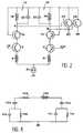
- the amplifier shown in this figurehas two input amplifiers 2, 4.
- the transmitter of each of these two amplifiersis connected to a inductance 6, 8 input capacity compensation (base-emitter capacity) of the bipolar transistor corresponding.
- Each of the two input amplifiersis associated with an amplifier 10, 12, so that perform a cascode assembly.
- the collector of each of these second amplifiers 10, 12see a circuit of load, or plug circuit, 14, 16 which is actually a LC circuit comprising on the one hand a capacity 20, 22 and on the other hand an inductor 18, 24, mounted in parallel.
- Two output transistors 26, 28are mounted as emitter-followers and each linked to a source of stream 30, 32. Their base is connected, respectively, at points A and B. These transistors therefore provide a signal image of the signal in the LC load circuit corresponding.
- this circuithas means 34, 36 making it possible to short-circuit the stage gain: thus, the input of each of the amplifiers 2, 4 is connected to the transmitter of each of the output amplifiers 26, 28. This has in particular as a consequence a change in the impedance entry.
- the second quality factors (of the second and fourth LC circuits)are for example weaker that the first quality factors (first and third LC circuits).
- each of the second and fourth LC circuitscan be integrated on a silicon substrate.
- An integrated inductor on siliconcannot be separated from its own elements parasites, due to the silicon substrate itself and to metallic materials of the inductor, which reduce the inductance quality factor. This has the effect to limit the possible gain obtained on a circuit parallel LC, at a given frequency.
- the third and fourth amplifierscan be realized in bipolar technology or in MOS technology.
- the means to carry out a switching of the device between a first and a second statethey may have first and second transistors MOS.
- a double gain amplifier deviceaccording to the invention, is illustrated in FIG. 3.
- references 2 and 4designate input amplifiers, each being associated with a compensation inductance 6, 8 (with inductance value L 6 , L 8 ) having the same function as that already exposed above in connection with FIGS. 1 and 2.
- Amplifiers 10 and 12produce, with amplifiers 2 and 4, cascode arrangements. All these amplifiers can be produced either in bipolar technology or in MOS technology.
- LC circuits 50, 54consisting respectively of an inductor 60 (of value L 2 ), 64 (of value L 1 ) each mounted in parallel with a capacity 70 ( C 2 ), 74 (C 1 ).
- the two circuits 50, 54are themselves mounted in parallel.
- a switch 80is associated with the circuit 54. Depending on the on or open state of this switch 80, the amplifier 10 sees the only load circuit 50 or the two load circuits 50, 54 in parallel.
- the second cascode assembly 4, 12is associated with two circuits 52, 56, each circuit being an LC circuit consisting of an inductor 62 (of value L 2 ), 66 (of value L 1 ) connected in parallel to a capacitor 72 (C 2 value), 76 (C 1 value).
- the circuit 56is associated with a switching means 82. Depending on the passing or closed state of this switch 82, the amplifier 12 sees, as a charging circuit, only the circuit 52, or else the two circuits 52, 56 arranged in parallel.
- the circuitalso includes two transistors 84, 86 whose bases are connected to the points A and B. These transistors provide an image signal of the signal in the corresponding charging circuit. Each of these two output transistors is associated with a current source 88, 90 and is mounted as a transmitter-follower.
- the output transistors and the load circuitsare connected to a supply rail 51 in V DC voltage.
- a current source 92ensures in the emitters of the input transistors 2, 4 a current constant. We can also, to impose such a constant current, impose constant polarization on the input of transistors 2, 4.
- the switching means 80, 82are of preferably made with MOS transistors, mounted in switches.
- the above circuithas been described with, associated with each of the transistors 10, 12 two circuits LC one of which can be switched, or not, in parallel with the other.
- the characteristics of these circuitsare chosen so that they have factors of different quality from each other. For example, if LC 54 circuit has a quality factor poor, while circuit 50 has a factor high quality, paralleling the two circuits results in a variation of the gain of the amplifier.
- a convenient means of producing LC circuits of different quality factorsconsists in producing inductances L 1 , L 2 of different quality factors. We therefore seek to achieve, for example: an inductance L 2 of high value and of quality factor high, and an inductance L 1 of low value and of low quality factor.
- FIG. 4shows a model of an inductor 100 made on silicon, with its parasitic elements: parasitic resistances 102, 108, 110 and parasitic capacitances 104, 106, 112, 114.
- the modification of the characteristics of inductance 100involves a modification resistance and stray capacitance values. For example, if the inductance has a larger contact surface with the silicon substrate, these associated parasitic elements (resistances, capacities) will be all the more important.
- inductorwith a poor quality factor
- said inductancecan then be associated with a capacity 76, 74 to constitute one of the circuits 54, 56: the quality factor of these circuits will be average, or poor (for example: Q ⁇ 2.5), and in any case different from that of circuits 50, 52 (for example: Q> 4) produced using another technology.
- the circuits 50, 52are for example made in ASGA technology or by mounting on printed circuit. We then have insulating substrates, so there is no element sufficient parasite. We can therefore obtain Q> 10.
- the bandwidth at -3dBis 410 MHz.
- the quality factor of the circuit, in this state,is therefore substantially equal to: Q ON ⁇ 1800 / 410 ⁇ 4.4.
- the gainis roughly equal to -0.4dB ⁇ 0.075dB and the bandwidth at -3dB is around 838MHz. This results in a quality factor Q ⁇ 1800 / 838 ⁇ 2.15.
- the transition from the state passing to the open state of the switchestherefore switches the quality factor of the circuit from a value of 4.4 to a value of 2.15.
- Figure 7shows, in decibels, the reflection coefficient at the input of the device, when the frequency varies from 1.7 to 1.9 GHz. We notes that, over this whole frequency range, the reflection coefficient is very low and does not vary that very few, that the switches 80, 82 are at the passing or open state (the curve is the same in both cases).
- Figure 8shows the input impedance of the device or, more exactly, the real part (curve I), and the imaginary part (curve II) of input impedance.
- the part input impedance imaginaryremains roughly equal to 0 over the entire frequency range 1.7-1.9 GHz, only the real part of the impedance having significant value.
Landscapes
- Engineering & Computer Science (AREA)
- Power Engineering (AREA)
- Amplifiers (AREA)
Abstract
Description
Translated fromFrenchL'invention concerne la réalisation d'undispositif amplificateur à gain commutable, enparticulier pour les applications radiofréquences (RF),dans un domaine de fréquences supérieur à 500 MHz, parexemple dans le domaine du gigahertz.The invention relates to the production of aswitchable gain amplifier device,particularly for radio frequency (RF) applications,in a frequency range greater than 500 MHz, byexample in the gigahertz domain.
On connaít déjà des réalisations de circuitsamplificateurs à bas bruit et à gain commutable.We already know some realizations of circuitsswitchable low noise and gain amplifiers.
La première réalisation est illustrée sur lafigure 1. L'amplificateur représenté sur cette figurecomporte deux amplificateurs d'entrée 2, 4. L'émetteurde chacun de ces deux amplificateurs est relié à uneinductance 6, 8 de compensation de la capacité d'entrée(capacité base-émetteur) du transistor bipolairecorrespondant.The first achievement is illustrated on thefigure 1. The amplifier shown in this figurehas two
Chacun des deux amplificateurs d'entrée estassocié à un amplificateur 10, 12, de manière àréaliser un montage cascode. Le collecteur de chacun deces deuxièmes amplificateurs 10, 12 voit un circuit decharge, ou circuit bouchon, 14, 16 qui est en fait uncircuit LC comportant d'une part une capacité 20, 22 etd'autre part une inductance 18, 24, montées enparallèle.Each of the two input amplifiers isassociated with an
Deux transistors de sortie 26, 28 sont montésen émetteurs-suiveurs et reliés chacun à une source decourant 30, 32. Leur base est reliée, respectivement,aux points A et B. Ces transistors fournissent donc unsignal image du signal dans le circuit LC de chargecorrespondant.Two
Afin de réaliser une commutation entre un étatà gain élevé et un état à bas gain, ce circuit comporte des moyens 34, 36 permettant de court-circuiter l'étagede gain : ainsi, l'entrée de chacun des amplificateurs2, 4 est connecté à l'émetteur de chacun desamplificateurs de sortie 26, 28. Ceci a en particulierpour conséquence une modification de l'impédanced'entrée. Par ailleurs, il y a toujours le risque, lorsde la commutation, de la création d'une rotation dephase entre les signaux d'entrée IN de l'amplificateur2 et NIN de l'amplificateur 4. Une telle rotation dephase peut entraíner une oscillation du dispositif,détruisant ainsi l'effet amplificateur : le dispositiffonctionne alors comme un oscillateur, et non pluscomme un amplificateur, avec ou sans gain.In order to switch between a statehigh gain and low gain state, this circuit hasmeans 34, 36 making it possible to short-circuit the stagegain: thus, the input of each of the
L'autre solution connue va être décrite enliaison avec la figure 2. Des références numériquesidentiques à celles de la figure 1 y désignent desmêmes éléments. Les inductances 6, 8 de compensationsont reliées à une source de courant 34 qui déterminele courant de l'étage d'entrée. Une variation ducourant de l'étage d'entrée entraíne une variation dela capacité de chacun des transistors d'entrée 2, 4 ;en effet, la capacité de ces transistors est liée aupositionnement du point de polarisation dudittransistor. De cette variation de la capacité de chaquetransistor d'entrée résulte une variation del'impédance d'entrée du système. Cependant, toutevariation de l'impédance d'entrée nuit à l'adaptationdu système, et cette deuxième solution n'est, de cepoint de vue, pas meilleure que la première.The other known solution will be described inlink with Figure 2. Numerical referencesidentical to those of FIG. 1 designate thereinsame elements.
Il se pose donc le problème de réaliser undispositif amplificateur à double gain, ou même à gainmultiple, dont la structure permette, quel que soit le gain sélectionné, de ne pas changer lescaractéristiques d'entrée de l'amplificateur.The problem therefore arises of making adouble gain, or even gain amplifier devicemultiple, whose structure allows, whatever theselected gain, not to change theamplifier input characteristics.
L'invention a pour objet un dispositifamplificateur à double gain comportant :
- un premier et un second amplificateurs d'entrée,
- un troisième et un quatrième amplificateurs réalisantavec les premier et second amplificateurs d'entrée,un premier et un second montages cascodes,
- un premier et un deuxième circuits LC, montés enparallèle et sur le troisième amplificateur, ainsiqu'un troisième et quatrième circuits LC, montés enparallèle et sur le quatrième amplificateur, lespremier et troisième circuits LC ayant chacun unpremier facteur de qualité, les deuxième et quatrièmecircuits LC ayant chacun un second facteur dequalité,
- des moyens pour commuter le dispositif amplificateurd'un premier état, dans lequel seuls les premier ettroisième circuits LC sont passants à un second étatdans lequel, à la fois, les quatre circuits LC sontdans un état passant.
- first and second input amplifiers,
- a third and a fourth amplifier producing, with the first and second input amplifiers, a first and a second cascode assembly,
- first and second LC circuits, mounted in parallel and on the third amplifier, as well as a third and fourth LC circuits, connected in parallel and on the fourth amplifier, the first and third LC circuits each having a first quality factor, the second and fourth LC circuits each having a second quality factor,
- means for switching the amplifier device from a first state, in which only the first and third LC circuits are on to a second state in which, at the same time, the four LC circuits are in an on state.
On dispose alors, pour chacun des deuxamplificateurs d'entrée, de deux circuits de facteur dequalité différents, qui permettent de modifier lavaleur du gain, à l'aide des moyens de commutation.Grâce aux troisième et quatrième amplificateursréalisant, avec les premier et second amplificateursd'entrée, des montages cascodes, l'impédance d'entréedu dispositif n'est pas modifiée, ce qui permet deconserver une adaptation d'impédance parfaite d'un trèsbon coefficient de réflexion.We then have, for each of the twoinput amplifiers, two factor circuitsdifferent quality, which allow to modify thegain value, using the switching means.Thanks to the third and fourth amplifiersrealizing, with the first and second amplifiersinput, cascode assemblies, input impedanceof the device is not modified, which allowskeep a perfect impedance matching of a verygood reflection coefficient.
Les seconds facteurs de qualité (des deuxièmeet quatrième circuits LC) sont par exemple plus faiblesque les premiers facteurs de qualité (des premier ettroisième circuits LC).The second quality factors (of the secondand fourth LC circuits) are for example weakerthat the first quality factors (first andthird LC circuits).
L'inductance de chacun des deuxième etquatrième circuits LC peut être intégrée sur unsubstrat en silicium. Une inductance intégrée sursilicium ne peut être séparée de ses propres élémentsparasites, dus au substrat silicium lui-même et auxmatériaux métalliques de l'inductance, qui réduisent lefacteur de qualité de l'inductance. Ceci a pour effetde limiter le gain possible obtenu sur un circuitparallèle LC, à une fréquence donnée. On réalise ainsiune inductance présentant un facteur de qualitémédiocre. Cette inductance, associée à une capacité C,forme un circuit LC de facteur de qualité égalementmédiocre. On peut donc utiliser une telle inductancepour réaliser par exemple les deuxième et quatrièmecircuits LC, qui présentent alors un faible facteur dequalité.The inductance of each of the second andfourth LC circuits can be integrated on asilicon substrate. An integrated inductor onsilicon cannot be separated from its own elementsparasites, due to the silicon substrate itself and tometallic materials of the inductor, which reduce theinductance quality factor. This has the effectto limit the possible gain obtained on a circuitparallel LC, at a given frequency. We thus realizean inductor with a quality factorpoor. This inductance, associated with a capacitance C,forms a quality factor LC circuit alsopoor. We can therefore use such an inductanceto make for example the second and fourthLC circuits, which then have a low factor ofquality.
Les troisième et quatrième amplificateurspeuvent être réalisés en technologie bipolaire ou bienen technologie MOS.The third and fourth amplifierscan be realized in bipolar technology orin MOS technology.
Quant aux moyens pour réaliser une commutationdu dispositif entre un premier et un second états, ilspeuvent comporter un premier et un second transistorsMOS.As for the means to carry out a switchingof the device between a first and a second state theymay have first and second transistorsMOS.
De toute façon, les caractéristiques etavantages de l'invention apparaítront mieux à lalumière de la description qui va suivre. Cettedescription porte sur les exemples de réalisation, donnés à titre explicatif et non limitatif, en seréférant à des dessins annexés sur lesquels :
- La figure 1 représente un premier dispositifà double gain, selon l'art antérieur.
- La figure 2 représente un autre dispositifconnu de l'art antérieur, également à double gain.
- La figure 3 représente un mode de réalisationd'un amplificateur à double gain selon l'invention.
- La figure 4 représente un modèle d'uneinductance intégrée sur silicium.
- La figure 5 représente des courbes de gaind'un dispositif selon l'invention, avec commutateursfermés.
- La figure 6 représente des courbes de gaind'un dispositif selon l'invention, avec commutateursouverts.
- La figure 7 représente le coefficient deréflexion en entrée d'un dispositif selon l'invention.
- La figure 8 représente les parties réelle etimaginaire de l'impédance d'entrée d'un dispositifselon l'invention.
- FIG. 1 represents a first double gain device, according to the prior art.
- FIG. 2 represents another device known from the prior art, also with double gain.
- FIG. 3 represents an embodiment of a double gain amplifier according to the invention.
- FIG. 4 represents a model of an inductance integrated on silicon.
- FIG. 5 represents gain curves of a device according to the invention, with closed switches.
- FIG. 6 represents gain curves of a device according to the invention, with open switches.
- FIG. 7 represents the reflection coefficient at the input of a device according to the invention.
- FIG. 8 represents the real and imaginary parts of the input impedance of a device according to the invention.
Un dispositif amplificateur à double gain,conforme à l'invention, est illustré en figure 3.A double gain amplifier device,according to the invention, is illustrated in FIG. 3.
Comme sur les figures 1 et 2, les références 2et 4 désignent des amplificateurs d'entrée, chacunétant associé à une inductance 6, 8 de compensation (devaleur d'inductance L6, L8) ayant la même fonction quecelle déjà exposée ci-dessus en liaison avec lesfigures 1 et 2. Des amplificateurs 10 et 12 réalisent,avec les amplificateurs 2 et 4, des montages cascodes. Tous ces amplificateurs peuvent être réalisés soit entechnologie bipolaire, soit en technologie MOS.As in FIGS. 1 and 2,
Au premier montage cas code constitué desamplificateurs 2 et 10 sont associés deux circuits LC50, 54 constitués respectivement d'une inductance 60(de valeur L2), 64 (de valeur L1) montées chacune enparallèle d'une capacité 70 (de valeur C2), 74 (devaleur C1). Les deux circuits 50, 54 sont montés eux-mêmesen parallèle. En outre, un commutateur 80 estassocié au circuit 54. Suivant l'état passant ou ouvertde ce commutateur 80, l'amplificateur 10 voit le seulcircuit de charge 50 ou bien les deux circuits decharge 50, 54 en parallèle.In the first case code assembly consisting of
De même, au deuxième montage cascode 4, 12 sontassociés deux circuits 52, 56, chaque circuit étant uncircuit LC constitué d'une inductance 62 (de valeurL2), 66 (de valeur L1) montée en parallèle à unecapacité 72 (de valeur C2), 76 (de valeur C1). Aucircuit 56 est associé un moyen de commutation 82.Selon l'état passant, ou fermé, de ce commutateur 82,l'amplificateur 12 voit, en tant que circuit de charge,uniquement le circuit 52, ou bien les deux circuits 52,56 disposés en parallèle.Similarly, the
Le circuit comporte en outre deux transistorsde sortie 84, 86 dont les bases sont reliées aux pointsA et B. Ces transistors fournissent un signal image dusignal dans le circuit de charge correspondant. Chacunde ces deux transistors de sortie est associé à unesource de courant 88, 90 et est monté en émetteur-suiveur.The circuit also includes two
Les transistors de sortie et les circuits decharge sont reliés à un rail d'alimentation 51 entension Vcc.The output transistors and the load circuits are connected to a supply rail 51 in VDC voltage.
Une source de courant 92 permet d'assurer dansles émetteurs des transistors d'entrée 2, 4 un courantconstant. On peut également, pour imposer un telcourant constant, imposer une polarisation constantesur l'entrée des transistors 2, 4.A
Les moyens de commutation 80, 82 sont depréférence réalisés avec des transistors MOS, montés eninterrupteurs.The switching means 80, 82 are ofpreferably made with MOS transistors, mounted inswitches.
Le circuit ci-dessus a été décrit avec,associés à chacun des transistors 10, 12 deux circuitsLC dont l'un peut être commuté, ou pas, en parallèleavec l'autre. Les caractéristiques de ces circuits sontchoisies de manière à ce qu'ils présentent des facteursde qualité différents l'un de l'autre. Par exemple, sile circuit LC 54 présente un facteur de qualitémédiocre, tandis que le circuit 50 présente un facteurde qualité élevé, la mise en parallèle des deuxcircuits résulte en une variation du gain del'amplificateur.The above circuit has been described with,associated with each of the
De préférence, on choisit L1, L2, C1, C2 de tellesorte que :
Un moyen commode de réaliser des circuits LC defacteurs de qualité différents consiste à réaliser desinductances L1, L2 de facteurs de qualité différents, Oncherche donc à réaliser, par exemple : une inductanceL2 de valeur élevée et de facteur de qualité élevé, et une inductance L1 de valeur faible et de facteur dequalité faible.A convenient means of producing LC circuits of different quality factors consists in producing inductances L1 , L2 of different quality factors. We therefore seek to achieve, for example: an inductance L2 of high value and of quality factor high, and an inductance L1 of low value and of low quality factor.
Ce résultat peut être obtenu en réalisant desinductances intégrées sur silicium. En effet, uneinductance intégrée sur silicium ne peut être séparéede ses éléments parasites qui réduisent le facteur dequalité de cette dernière : il en résulte unelimitation du gain possible obtenu sur un circuit decharge LC à une fréquence donnée. La figure 4représente un modèle d'une inductance 100 réalisée sursilicium, avec ses éléments parasites : résistancesparasites 102, 108, 110 et capacités parasites 104,106, 112, 114. La modification des caractéristiques del'inductance 100 entraíne une modification des valeursdes résistances et des capacités parasites. Parexemple, si l'inductance présente une surface decontact plus large avec le substrat en silicium, ceséléments parasites associés (résistances, capacités)seront d'autant plus importants. Le facteur de qualitéde l'inductance, pour une pulsation ω donnée, résulte,au premier ordre, de la formule :
Il est alors possible de réaliser uneinductance présentant un facteur de qualité médiocre,ladite inductance pouvant ensuite être associée à unecapacité 76, 74 pour constituer l'un des circuits 54,56 : le facteur de qualité de ces circuits sera moyen,ou médiocre (par exemple : Q<2,5), et en tout casdifférent de celui des circuits 50, 52 (par exemple :Q>4) réalisés selon une autre technologie. Les circuits50, 52 sont par exemple réalisés en technologie ASGA oupar montage sur circuit imprimé. On a alors des substrats isolants, il n'y a donc pas d'élémentparasite suffisant. On peut donc obtenir Q>10.It is then possible to carry out ainductor with a poor quality factor,said inductance can then be associated with a
Un procédé pour réaliser une inductance sur unsubstrat en silicium est par ailleurs décrit dansl'article de J. Craninckx et al., intitulé "A 1,8 GHzlow-phase-noise CMOS VCO using optimized hollow spiralinductors" paru dans IEEE Journal of solid-StateCircuits, vol. 32, n° 5, 1997.A method for making an inductance on asilicon substrate is further described inthe article by J. Craninckx et al., entitled "At 1.8 GHzlow-phase-noise CMOS VCO using optimized hollow spiralinductors "published in IEEE Journal of solid-StateTours, vol. 32, no.5, 1997.
Cet article décrit ainsi l'effet parasite dusubstrat sur l'inductance et montre comment peut êtreréalisée une inductance. L'article de Y.Koutsoyannopoulos et al. Intitulé "A Generic CAD Modelfor arbitrarily shaped and multi-layer integratedinductors on silicon substrates", Proceedings of theESSCIRC 97 Conference, p. 320-323, décrit lesphénomènes parasites sur une inductance et tente de lesmodéliser.This article describes the parasitic effect ofsubstrate on the inductor and shows how can bemade an inductor. The article by Y.Koutsoyannopoulos et al. Entitled "A Generic CAD Modelfor arbitrarily shaped and multi-layer integratedinductors on silicon substrates ", Proceedings of theESSCIRC 97 Conference, p. 320-323, describes theparasitic phenomena on an inductor and tries tomodel.
Selon un exemple, un dispositif amplificateurselon l'invention a été réalisé, avec lescaractéristiques suivantes :
- C1=2,5 pF,
- C2=0,8 pF,
- L1=0,817 nH,
- L2= 5, 02 nH,
- L6=L8=0,258 nH,
- les
transistors
- C1 = 2.5 pF,
- C2 = 0.8 pF,
- L1 = 0.817 nH,
- L2 = 5.02 nH,
- L6 = L8 = 0.258 nH,
transistors
La figure 5 représente la courbe de gain G ducircuit <G1=VNOUT/VNIN, G2=VOUT/VIN) en fonction de lafréquence lorsque celle-ci varie de 1,55 à 2,05 GHz, etlorsque les commutateurs 80, 82 sont à l'état passant :on obtient un gain G à peu près égal à 17,55 dB ± 0,024 dB pour ω=1,8GHz. La bande passante à -3dB est de410 MHz. Le facteur de qualité du circuit, dans cetétat, est donc sensiblement égal à : QON≈1800/410≈4,4.FIG. 5 represents the gain curve G of the circuit <G1 = VNOUT / VNIN , G2 = VOUT / VIN ) as a function of the frequency when the latter varies from 1.55 to 2.05 GHz, and when the
La figure 6 montre également l'évolution dugain (G1=VNOUT/VNIN ; G2=VOUT/VIN) en fonction de lafréquence, lorsque celle-ci varie de 1,35 à 2,4 GHz,les deux commutateurs 80 et 82 étant ouverts. Le gainest à peu près égal à -0,4dB ± 0,075dB et la bandepassante à -3dB est d'environ 838MHz. Il en résulte unfacteur de qualité Q≈1800/838≈2,15. Le passage del'état passant à l'état ouvert des commutateurs faitdonc basculer le facteur de qualité du circuit d'unevaleur de 4,4 à une valeur de 2,15.FIG. 6 also shows the evolution of the gain (G1 = VNOUT / VNIN ; G2 = VOUT / VIN ) as a function of frequency, when the latter varies from 1.35 to 2.4 GHz, the two
La figure 7 représente, en décibels, lecoefficient de réflexion en entrée du dispositif,lorsque la fréquence varie de 1,7 à 1,9 GHz. Onconstate que, sur toute cette gamme de fréquences, lecoefficient de réflexion est très faible et ne varieque très peu, que les commutateurs 80, 82 soient àl'état passant ou ouvert (la courbe est la même dansles deux cas).Figure 7 shows, in decibels, thereflection coefficient at the input of the device,when the frequency varies from 1.7 to 1.9 GHz. Wenotes that, over this whole frequency range, thereflection coefficient is very low and does not varythat very few, that the
La figure 8 représente l'impédance d'entrée dudispositif ou, plus exactement, la partie réelle(courbe I), et la partie imaginaire (courbe II) del'impédance d'entrée. On constate que la partieimaginaire de l'impédance d'entrée reste à peu prèségale à 0 sur tout le domaine de fréquences 1,7-1,9GHz, seule la partie réelle de l'impédance ayantune valeur significative.Figure 8 shows the input impedance of thedevice or, more exactly, the real part(curve I), and the imaginary part (curve II) ofinput impedance. We see that the partinput impedance imaginary remains roughlyequal to 0 over the entire frequency range 1.7-1.9GHz, only the real part of the impedance havingsignificant value.
Ces résultats montrent bien qu'une commutationefficace est obtenue, qui permet de passer d'un gain de17,5 dB à un gain de -0,4dB, sans variation de l'impédance d'entrée et sans modification ducoefficient de réflexion. Comme déjà expliqué ci-dessus,on peut monter plusieurs circuits LC enparallèle à chaque circuit 50, 52 et obtenir unecommutation entre plusieurs états, une valeur de gainétant associée à chaque état. Par exemple, on peutmonter deux circuits LC en parallèle à chacun descircuits 50, 52, un commutateur étant associé à chacunde ces circuits parallèles. On peut donc passer alors,par exemple, d'une valeur de gain de 17,5 dB à unevaleur de 10 dB ou à une valeur de -0,5 dB.These results clearly show that switchingefficient is obtained, which allows to pass from a gain of17.5 dB at a gain of -0.4dB, without variation ofinput impedance and without modification of thereflection coefficient. As already explained above,we can mount several LC circuits inparallel to each
Claims (7)
Translated fromFrenchApplications Claiming Priority (2)
| Application Number | Priority Date | Filing Date | Title |
|---|---|---|---|
| FR9713232AFR2770053B1 (en) | 1997-10-22 | 1997-10-22 | DOUBLE GAIN AMPLIFIER CIRCUIT |
| FR9713232 | 1997-10-22 |
Publications (2)
| Publication Number | Publication Date |
|---|---|
| EP0911969A1true EP0911969A1 (en) | 1999-04-28 |
| EP0911969B1 EP0911969B1 (en) | 2004-02-25 |
Family
ID=9512513
Family Applications (1)
| Application Number | Title | Priority Date | Filing Date |
|---|---|---|---|
| EP98402604AExpired - LifetimeEP0911969B1 (en) | 1997-10-22 | 1998-10-20 | Amplifier circuit with dual gain |
Country Status (4)
| Country | Link |
|---|---|
| US (1) | US6023192A (en) |
| EP (1) | EP0911969B1 (en) |
| DE (1) | DE69821861T2 (en) |
| FR (1) | FR2770053B1 (en) |
Cited By (4)
| Publication number | Priority date | Publication date | Assignee | Title |
|---|---|---|---|---|
| FR2798016A1 (en)* | 1999-08-31 | 2001-03-02 | St Microelectronics Sa | AMPLIFIER CIRCUIT WITH DOUBLE BANDWIDTH AND RADIO FREQUENCY RECEIVING HEAD |
| WO2002017477A3 (en)* | 2000-08-25 | 2002-10-03 | Sige Semiconductor Inc | Mixer with image reject filter |
| CN103579146A (en)* | 2012-07-31 | 2014-02-12 | 株式会社东芝 | Semiconductor device |
| WO2016011036A1 (en)* | 2014-07-14 | 2016-01-21 | Finisar Corporation | Multi-rate clock buffer |
Families Citing this family (19)
| Publication number | Priority date | Publication date | Assignee | Title |
|---|---|---|---|---|
| JP3347615B2 (en)* | 1996-11-28 | 2002-11-20 | 富士通株式会社 | Semiconductor integrated circuit and optical transmission module |
| US6297685B1 (en)* | 2000-06-14 | 2001-10-02 | International Business Machines Corporation | High-speed fully-compensated low-voltage differential driver/translator circuit arrangement |
| US6683498B2 (en)* | 2000-07-03 | 2004-01-27 | Broadcom Corporation | Protection circuit for extending headroom with off-chip inductors |
| FR2811827B1 (en)* | 2000-07-12 | 2002-10-11 | St Microelectronics Sa | LOW NOISE AMPLIFICATION DEVICE, PARTICULARLY FOR A CELLULAR MOBILE TELEPHONE |
| US6342813B1 (en)* | 2000-08-24 | 2002-01-29 | International Business Machines Corporation | Variable gain amplifier |
| FR2823031B1 (en)* | 2001-03-27 | 2003-07-04 | St Microelectronics Sa | GAIN SWITCHING AMPLIFIER DEVICE, PARTICULARLY FOR A CELLULAR MOBILE TELEPHONE |
| US6424222B1 (en)* | 2001-03-29 | 2002-07-23 | Gct Semiconductor, Inc. | Variable gain low noise amplifier for a wireless terminal |
| NL1017773C2 (en)* | 2001-04-04 | 2002-10-07 | Ericsson Telefon Ab L M | Amplifier-mixer device. |
| DE10132800C1 (en)* | 2001-07-06 | 2003-01-30 | Infineon Technologies Ag | Low noise amplifier circuit |
| AU2003246494A1 (en)* | 2002-07-24 | 2004-02-09 | Sirific Wireless Corporation | Multi-standard amplifier |
| US6838939B2 (en)* | 2003-04-29 | 2005-01-04 | Intel Corporation | Amplifier apparatus, method, and system |
| JP4543805B2 (en)* | 2003-08-07 | 2010-09-15 | 富士通株式会社 | Differential amplifier circuit |
| US7286013B2 (en)* | 2003-09-18 | 2007-10-23 | Avago Technologies Wireless Ip (Singapore) Pte Ltd | Coupled-inductance differential amplifier |
| US7265623B2 (en)* | 2004-08-03 | 2007-09-04 | Scintera Networks, Inc. | Differential amplifier having independently tunable base gain, peak gain and boost frequency, and uses of same |
| US7190226B2 (en)* | 2004-08-27 | 2007-03-13 | Scintera Networks | Analog delay chain having more uniformly distributed capacitive loads and analog delay cell for use in chain |
| US7170349B2 (en)* | 2004-09-21 | 2007-01-30 | Scintera Networks, Inc. | Low voltage broadband gain cell |
| US20070024377A1 (en)* | 2005-07-28 | 2007-02-01 | Xuezhen Wang | Impedance matching techiques for multi-band or wideband RF amplifiers and associated amplifier designs |
| DE102006004952A1 (en)* | 2006-02-01 | 2007-08-16 | Atmel Germany Gmbh | Differential amplifier and radio system with differential amplifier |
| GB0609739D0 (en)* | 2006-05-17 | 2006-06-28 | Univ Bradford | High frequency low noise amplifier |
Citations (6)
| Publication number | Priority date | Publication date | Assignee | Title |
|---|---|---|---|---|
| US3333200A (en)* | 1963-10-18 | 1967-07-25 | Gen Electric | Transistorized autodyne converter and amplifier circuit arrangement |
| US3611001A (en)* | 1969-05-05 | 1971-10-05 | Burroughs Corp | High-speed current-switching amplifiers |
| DE2829164A1 (en)* | 1978-07-03 | 1980-01-17 | Philips Patentverwaltung | Tunable HF oscillating circuit for selective amplifier and oscillator - has all components except inductances consisting of integrated circuits |
| US4520324A (en)* | 1983-03-11 | 1985-05-28 | National Semiconductor Corporation | MOS Gain controlled amplifier |
| EP0475118A2 (en)* | 1990-08-31 | 1992-03-18 | Fujitsu Limited | Current mirror amplifier circuit and method of driving the same |
| US5313207A (en)* | 1992-12-22 | 1994-05-17 | Mitsubishi Denki Kabushiki Kaisha | Differential subtracter improved for higher accuracy and A/D converter including the same |
Family Cites Families (4)
| Publication number | Priority date | Publication date | Assignee | Title |
|---|---|---|---|---|
| US3743863A (en)* | 1971-11-03 | 1973-07-03 | Motorola Inc | Transistorized electronic circuit employing resistorless bias network |
| IT1091707B (en)* | 1977-11-02 | 1985-07-06 | Cselt Centro Studi Lab Telecom | SYSTEM FOR THE SUPPLY OF STAGE SELECTIVE AMPLIFIERS IN CASCADE |
| US4339728A (en)* | 1980-02-11 | 1982-07-13 | National Semiconductor Corporation | Radio receiver signal amplifier and AGC circuit |
| US4663599A (en)* | 1985-05-21 | 1987-05-05 | General Electric Company | Integrated circuit amplifier module |
- 1997
- 1997-10-22FRFR9713232Apatent/FR2770053B1/ennot_activeExpired - Fee Related
- 1998
- 1998-10-09USUS09/169,518patent/US6023192A/ennot_activeExpired - Lifetime
- 1998-10-20EPEP98402604Apatent/EP0911969B1/ennot_activeExpired - Lifetime
- 1998-10-20DEDE69821861Tpatent/DE69821861T2/ennot_activeExpired - Fee Related
Patent Citations (6)
| Publication number | Priority date | Publication date | Assignee | Title |
|---|---|---|---|---|
| US3333200A (en)* | 1963-10-18 | 1967-07-25 | Gen Electric | Transistorized autodyne converter and amplifier circuit arrangement |
| US3611001A (en)* | 1969-05-05 | 1971-10-05 | Burroughs Corp | High-speed current-switching amplifiers |
| DE2829164A1 (en)* | 1978-07-03 | 1980-01-17 | Philips Patentverwaltung | Tunable HF oscillating circuit for selective amplifier and oscillator - has all components except inductances consisting of integrated circuits |
| US4520324A (en)* | 1983-03-11 | 1985-05-28 | National Semiconductor Corporation | MOS Gain controlled amplifier |
| EP0475118A2 (en)* | 1990-08-31 | 1992-03-18 | Fujitsu Limited | Current mirror amplifier circuit and method of driving the same |
| US5313207A (en)* | 1992-12-22 | 1994-05-17 | Mitsubishi Denki Kabushiki Kaisha | Differential subtracter improved for higher accuracy and A/D converter including the same |
Cited By (8)
| Publication number | Priority date | Publication date | Assignee | Title |
|---|---|---|---|---|
| FR2798016A1 (en)* | 1999-08-31 | 2001-03-02 | St Microelectronics Sa | AMPLIFIER CIRCUIT WITH DOUBLE BANDWIDTH AND RADIO FREQUENCY RECEIVING HEAD |
| EP1081849A1 (en)* | 1999-08-31 | 2001-03-07 | STMicroelectronics SA | Dual band amplifier circui and radio frequency receiving unit |
| US6366166B1 (en) | 1999-08-31 | 2002-04-02 | Stmicroelectronics S.A. | Double pass band amplifier circuit and a radio frequency reception head |
| WO2002017477A3 (en)* | 2000-08-25 | 2002-10-03 | Sige Semiconductor Inc | Mixer with image reject filter |
| US6681103B1 (en) | 2000-08-25 | 2004-01-20 | Sige Semiconductor Inc. | On-chip image reject filter |
| CN103579146A (en)* | 2012-07-31 | 2014-02-12 | 株式会社东芝 | Semiconductor device |
| WO2016011036A1 (en)* | 2014-07-14 | 2016-01-21 | Finisar Corporation | Multi-rate clock buffer |
| US9847776B2 (en) | 2014-07-14 | 2017-12-19 | Finisar Corporation | Multi-rate clock buffer |
Also Published As
| Publication number | Publication date |
|---|---|
| DE69821861D1 (en) | 2004-04-01 |
| FR2770053A1 (en) | 1999-04-23 |
| US6023192A (en) | 2000-02-08 |
| EP0911969B1 (en) | 2004-02-25 |
| DE69821861T2 (en) | 2004-12-30 |
| FR2770053B1 (en) | 2000-01-07 |
Similar Documents
| Publication | Publication Date | Title |
|---|---|---|
| EP0911969B1 (en) | Amplifier circuit with dual gain | |
| EP2246931B1 (en) | Common-mode filter with coupled inductors | |
| EP0660512B1 (en) | Phase shifter amplifier and its application in a recombiner circuit | |
| EP1172929B1 (en) | Low noise amplifier arrangement especially for cellular mobile telephone | |
| FR2926689A1 (en) | ELECTRICAL DEVICE WITH RESONATOR WITH BROAD RANGE OF FREQUENCY VARIATION | |
| FR2829316A1 (en) | CONTROL ATTENUATOR | |
| FR2848721A1 (en) | FREQUENCY SELECTIVE MODE CHANGE TRANSFORMER | |
| EP0387954B1 (en) | Pass-band filter with adjustable band-width | |
| FR2740924A1 (en) | INPUT PROTECTION FOR A HIGH BANDWIDTH AMPLIFIER | |
| EP2178152A1 (en) | Electronic switching device for high-frequency signals | |
| EP0414328A1 (en) | Differential amplifier with capacitive coupling | |
| EP0130260B1 (en) | Interface module for telephone lines | |
| FR2640445A1 (en) | CIRCUIT FOR SWITCHING AN INDUCTIVE ELEMENT FOR A PHASE CIRCUIT | |
| FR2749718A1 (en) | LOW NOISE AMPLIFIER | |
| EP0596568B1 (en) | Semiconductor device comprising a monolithic integrated distribited amplifier circuit with wide bandwidth and high gain | |
| WO2002017480A1 (en) | Linear pre-amplifier for radio-frequency power amplifier | |
| EP0199332B1 (en) | Wide-band receiver for optical signals | |
| FR2653615A1 (en) | FILTER CELL AND CORRESPONDING FILTER. | |
| FR2730363A1 (en) | HIGH FREQUENCY HIGH GAIN AMPLIFIER AND RESONANT CIRCUIT OSCILLATOR PROVIDED WITH SUCH AMPLIFIER | |
| EP0978949A1 (en) | Radio frequency switch | |
| EP0347985B1 (en) | Active allpass ultra-high frequency circuit | |
| EP1047132A1 (en) | Integrated circuit device with inductance of high quality factor | |
| EP0120756A1 (en) | Oscillator comprising high-frequency bandpass amplifier having an adaptable impedance | |
| FR3047606A1 (en) | ENTIRELY INTEGRATED LOW NOISE AMPLIFIER. | |
| EP0606943B1 (en) | Switching device for switching television signals in a cable distribution system |
Legal Events
| Date | Code | Title | Description |
|---|---|---|---|
| PUAI | Public reference made under article 153(3) epc to a published international application that has entered the european phase | Free format text:ORIGINAL CODE: 0009012 | |
| AK | Designated contracting states | Kind code of ref document:A1 Designated state(s):DE FR GB IT | |
| AX | Request for extension of the european patent | Free format text:AL;LT;LV;MK;RO;SI | |
| 17P | Request for examination filed | Effective date:19991014 | |
| AKX | Designation fees paid | Free format text:DE FR GB IT | |
| RAP1 | Party data changed (applicant data changed or rights of an application transferred) | Owner name:STMICROELECTRONICS S.A. | |
| GRAP | Despatch of communication of intention to grant a patent | Free format text:ORIGINAL CODE: EPIDOSNIGR1 | |
| GRAS | Grant fee paid | Free format text:ORIGINAL CODE: EPIDOSNIGR3 | |
| GRAA | (expected) grant | Free format text:ORIGINAL CODE: 0009210 | |
| AK | Designated contracting states | Kind code of ref document:B1 Designated state(s):DE FR GB IT | |
| PG25 | Lapsed in a contracting state [announced via postgrant information from national office to epo] | Ref country code:IT Free format text:LAPSE BECAUSE OF FAILURE TO SUBMIT A TRANSLATION OF THE DESCRIPTION OR TO PAY THE FEE WITHIN THE PRESCRIBED TIME-LIMIT;WARNING: LAPSES OF ITALIAN PATENTS WITH EFFECTIVE DATE BEFORE 2007 MAY HAVE OCCURRED AT ANY TIME BEFORE 2007. THE CORRECT EFFECTIVE DATE MAY BE DIFFERENT FROM THE ONE RECORDED. Effective date:20040225 | |
| REG | Reference to a national code | Ref country code:GB Ref legal event code:FG4D Free format text:NOT ENGLISH | |
| REF | Corresponds to: | Ref document number:69821861 Country of ref document:DE Date of ref document:20040401 Kind code of ref document:P | |
| GBT | Gb: translation of ep patent filed (gb section 77(6)(a)/1977) | Effective date:20040520 | |
| PLBE | No opposition filed within time limit | Free format text:ORIGINAL CODE: 0009261 | |
| STAA | Information on the status of an ep patent application or granted ep patent | Free format text:STATUS: NO OPPOSITION FILED WITHIN TIME LIMIT | |
| 26N | No opposition filed | Effective date:20041126 | |
| PGFP | Annual fee paid to national office [announced via postgrant information from national office to epo] | Ref country code:DE Payment date:20060928 Year of fee payment:9 | |
| PGFP | Annual fee paid to national office [announced via postgrant information from national office to epo] | Ref country code:GB Payment date:20071129 Year of fee payment:10 Ref country code:FR Payment date:20071129 Year of fee payment:10 | |
| PG25 | Lapsed in a contracting state [announced via postgrant information from national office to epo] | Ref country code:DE Free format text:LAPSE BECAUSE OF NON-PAYMENT OF DUE FEES Effective date:20080501 | |
| GBPC | Gb: european patent ceased through non-payment of renewal fee | Effective date:20081020 | |
| REG | Reference to a national code | Ref country code:FR Ref legal event code:ST Effective date:20090630 | |
| PG25 | Lapsed in a contracting state [announced via postgrant information from national office to epo] | Ref country code:FR Free format text:LAPSE BECAUSE OF NON-PAYMENT OF DUE FEES Effective date:20081031 | |
| PG25 | Lapsed in a contracting state [announced via postgrant information from national office to epo] | Ref country code:GB Free format text:LAPSE BECAUSE OF NON-PAYMENT OF DUE FEES Effective date:20081020 |