EP0905544B1 - A method of fabricating a liquid crystal display - Google Patents
A method of fabricating a liquid crystal displayDownload PDFInfo
- Publication number
- EP0905544B1 EP0905544B1EP98122876AEP98122876AEP0905544B1EP 0905544 B1EP0905544 B1EP 0905544B1EP 98122876 AEP98122876 AEP 98122876AEP 98122876 AEP98122876 AEP 98122876AEP 0905544 B1EP0905544 B1EP 0905544B1
- Authority
- EP
- European Patent Office
- Prior art keywords
- layer
- substrate
- transparent
- light influencing
- light
- Prior art date
- Legal status (The legal status is an assumption and is not a legal conclusion. Google has not performed a legal analysis and makes no representation as to the accuracy of the status listed.)
- Expired - Lifetime
Links
Images

Classifications
- G—PHYSICS
- G02—OPTICS
- G02F—OPTICAL DEVICES OR ARRANGEMENTS FOR THE CONTROL OF LIGHT BY MODIFICATION OF THE OPTICAL PROPERTIES OF THE MEDIA OF THE ELEMENTS INVOLVED THEREIN; NON-LINEAR OPTICS; FREQUENCY-CHANGING OF LIGHT; OPTICAL LOGIC ELEMENTS; OPTICAL ANALOGUE/DIGITAL CONVERTERS
- G02F1/00—Devices or arrangements for the control of the intensity, colour, phase, polarisation or direction of light arriving from an independent light source, e.g. switching, gating or modulating; Non-linear optics
- G02F1/01—Devices or arrangements for the control of the intensity, colour, phase, polarisation or direction of light arriving from an independent light source, e.g. switching, gating or modulating; Non-linear optics for the control of the intensity, phase, polarisation or colour
- G02F1/13—Devices or arrangements for the control of the intensity, colour, phase, polarisation or direction of light arriving from an independent light source, e.g. switching, gating or modulating; Non-linear optics for the control of the intensity, phase, polarisation or colour based on liquid crystals, e.g. single liquid crystal display cells
- G02F1/133—Constructional arrangements; Operation of liquid crystal cells; Circuit arrangements
- G02F1/1333—Constructional arrangements; Manufacturing methods
- G02F1/1335—Structural association of cells with optical devices, e.g. polarisers or reflectors
- G02F1/133509—Filters, e.g. light shielding masks
- G02F1/133514—Colour filters
- G02F1/133516—Methods for their manufacture, e.g. printing, electro-deposition or photolithography
- G—PHYSICS
- G02—OPTICS
- G02F—OPTICAL DEVICES OR ARRANGEMENTS FOR THE CONTROL OF LIGHT BY MODIFICATION OF THE OPTICAL PROPERTIES OF THE MEDIA OF THE ELEMENTS INVOLVED THEREIN; NON-LINEAR OPTICS; FREQUENCY-CHANGING OF LIGHT; OPTICAL LOGIC ELEMENTS; OPTICAL ANALOGUE/DIGITAL CONVERTERS
- G02F1/00—Devices or arrangements for the control of the intensity, colour, phase, polarisation or direction of light arriving from an independent light source, e.g. switching, gating or modulating; Non-linear optics
- G02F1/01—Devices or arrangements for the control of the intensity, colour, phase, polarisation or direction of light arriving from an independent light source, e.g. switching, gating or modulating; Non-linear optics for the control of the intensity, phase, polarisation or colour
- G02F1/13—Devices or arrangements for the control of the intensity, colour, phase, polarisation or direction of light arriving from an independent light source, e.g. switching, gating or modulating; Non-linear optics for the control of the intensity, phase, polarisation or colour based on liquid crystals, e.g. single liquid crystal display cells
- G02F1/133—Constructional arrangements; Operation of liquid crystal cells; Circuit arrangements
- G02F1/1333—Constructional arrangements; Manufacturing methods
- G02F1/1335—Structural association of cells with optical devices, e.g. polarisers or reflectors
- G02F1/133509—Filters, e.g. light shielding masks
- G02F1/133512—Light shielding layers, e.g. black matrix
Definitions
- High resolution electronic optical systemssuch as for example, either active or passive liquid crystal displays, and contact image scanning systems are today well known in the commercial fields. While systems of the type described above have been generally successful in fulfilling their intended purposes and have found commercial acceptance, these systems exhibit several deficiencies.
- the deficiency specifically addressed hereinrelates to the fact that heretofore, the light influencing elements used in high resolution optical systems, to, for example, polarize or color filter light passing therethrough, have been very difficult to fabricate, often requiring up to ten or more fabrication steps.
- the result of having so many fabrication stepsis that the manufacturing process is very costly, and further that the process is susceptible to producing high amounts of unacceptable or scrap light influencing elements. This of course further increases the cost of the light influencing elements.
- FIG. 11illustrates in a step-by-step manner, the conventional photolithographic method of fabricating color filter elements for liquid crystal display.
- a color filter elementis fabricated by depositing a layer of transparent gelatine glue, known in the art as "fish glue" atop the display electrodes, which have already been formed upon a transparent substrate. A photomask is then applied so that the transparent gelatine glue is removed from all ares other than atop a display electrode.
- a light influencing elementidentified generally by the reference numeral 10.
- the light influencing element 10will typically be employed as a color filter element, as is explained in greater detail hereinbelow, though it is to be understood that such an element may be employed in a number of different applications including, but not limited to, a light diffuser, a light collimator, a light polarizer or a light rotating element.
- the light influencing elementmay be adapted to provide an optical effect upon radiation not in the range of visible light.
- said elementmay be adapted to filter certain wavelengths of radiation such as infra-red or ultra-violet.
- the openings 16themselves may be formed by any one of a number of techniques, such as a conventional photolithographic and etch technique.
- the openings 16are formed by employing a high resolution i.e., capable of at least micron scale resolution, high power laser device, such as an excimer laser adapted to cut a plurality of similarly sized and shaped openings in the layer of substantially opaque material 14.
- a high resolution i.e., capable of at least micron scale resolution, high power laser devicesuch as an excimer laser adapted to cut a plurality of similarly sized and shaped openings in the layer of substantially opaque material 14.
- the element 10 of Figure 1may be adapted, as mentioned above to use in conjunction with a liquid crystal display.
- the excimer lasershould be able to form a plurality of openings 16 formed in a highly packed N x M matrix of rows and columns.
- a light influencing materialselected to provide a desired optical effect.
- the light influencing materialis to be employed as a color filter element, dye, ink such as the ink used in so-called ink-jet technology or other color pigments may be disposed in said openings 16.
- the dyes or pigmentswhich may be either of the additive or subtractive variety, would be disposed in a manner and to a thickness sufficient to, for example, color white light red as it passed therethrough.
- the element 10may then be adapted to serve as the foundation upon which an entire electronic optical device, or some subassembly thereof, is fabricated.
- the element 10is arranged as a matrix of 3 x 3 openings of which Figure 2 illustrates but six openings in a row of 8, though it is to be understood that the element 10 may be arranged to include any number of openings arranged in rows and columns, or in any other fashion, such as triads or stripes.
- the substrate 12 with the layer of opaque material 14 having a plurality of openings 16a-16f formed thereinis placed in relatively close proximity to means for injecting a light influencing material into said openings.
- these injection meanscomprise three injection nozzles 21a, 21b, and 21c which are adapted to inject, for example, dye, ink or color pigments into the openings 16a-16f, in so called "ink-jet" fashion.
- the nozzles 21a-21c or the substrate 12may either be fitted with apparatus to effect relative movement therebetween so that one or more nozzles may be used to fill each opening.
- the substrate 40may be formed from other substantially transparent materials such as a clear plastic or other polymeric material which may be either rigid, as glass, or flexible as would be the case for a thin, polymeric material such as a layer of kapton, or polycarbonate materials of the type that are currently used in numerous applications wherein considerations such as hardness and optical clarity are of paramount importance.
- a clear plastic or other polymeric materialwhich may be either rigid, as glass, or flexible as would be the case for a thin, polymeric material such as a layer of kapton, or polycarbonate materials of the type that are currently used in numerous applications wherein considerations such as hardness and optical clarity are of paramount importance.
- the second substrate 40has disposed thereupon a layer of transparent conductive material such as a transparent conductive oxide material 42.
- transparent conductive oxidesinclude indium oxide, tin oxide, indium tin oxide, cadmium sulfate and combinations thereof.
- the layer of transparent conductive material 42may be either a continuous layer or may be a patterned layer of display electrodes formed by conventional photolithographic processes.
- the second substrate 40may also have disposed thereon other micro-electronic devices such as transistors or diodes which enhance the switching and other performance of the display.
- the second substrate 40is arranged so that the second layer of transparent conductive material 42 is spacedly disposed from and facing the patterned layer of transparent conductive material disposed on the first substrate 12.
Landscapes
- Physics & Mathematics (AREA)
- Nonlinear Science (AREA)
- Mathematical Physics (AREA)
- Chemical & Material Sciences (AREA)
- Crystallography & Structural Chemistry (AREA)
- General Physics & Mathematics (AREA)
- Optics & Photonics (AREA)
- Engineering & Computer Science (AREA)
- Manufacturing & Machinery (AREA)
- Optical Filters (AREA)
- Liquid Crystal (AREA)
- Particle Formation And Scattering Control In Inkjet Printers (AREA)
Description
- The present invention generally relates to a method of fabricating a liquidcrystal display including high resolution color filter elements.
- Efficient production of full color systems for usein cameras, television, etc. have been contemplatedsince at least as early as the late 1950's and aregenerally discussed in an article which appeared in theMay 1959 edition ofScientific American. Reference mayalso be made to United States Patent Nos. 3,382,317,3,443,023 and 3,443,025. As optical system technology evolved, so too did the technology employed inproviding full color thereto.
- High resolution electronic optical systems, suchas for example, either active or passive liquid crystaldisplays, and contact image scanning systems are todaywell known in the commercial fields. While systems ofthe type described above have been generally successfulin fulfilling their intended purposes and have foundcommercial acceptance, these systems exhibit severaldeficiencies. The deficiency specifically addressedherein relates to the fact that heretofore, the lightinfluencing elements used in high resolution opticalsystems, to, for example, polarize or color filterlight passing therethrough, have been very difficult tofabricate, often requiring up to ten or morefabrication steps. The result of having so manyfabrication steps is that the manufacturing process isvery costly, and further that the process issusceptible to producing high amounts of unacceptableor scrap light influencing elements. This of coursefurther increases the cost of the light influencingelements.
- As noted above, color liquid crystal displaydevices are well known in the art, and one exemplarysuch device is set forth in United States Patent No.4,632,514 toOgawa, et al, entitled "COLOR LIQUIDCRYSTAL DISPLAY APPARATUS. The '514 patent describesa color, twisted nematic type display wherein the layerof liquid crystal material is varied depending upon thecolor imparted to each picture element of the display.Ogawa, et al describe the need to terrace the layers offilter materials, which, as will be noted in greaterdetail hereinbelow, require additional fabricationsteps in the manufacture of a display.
- The commonly accepted method of fabricating lightinfluencing elements for high resolution opticalsystems, particularly liquid crystal displays, is setforth in an article entitledMulticolored LiquidCrystal Displays, published inOptical Engineering,Vol.23 No.3, May/June 1984. More particularly, figure11 thereof illustrates in a step-by-step manner, theconventional photolithographic method of fabricatingcolor filter elements for liquid crystal display. Asa perusal of said article teaches, a color filterelement is fabricated by depositing a layer oftransparent gelatine glue, known in the art as "fishglue" atop the display electrodes, which have alreadybeen formed upon a transparent substrate. A photomaskis then applied so that the transparent gelatine glueis removed from all ares other than atop a displayelectrode. Thereafter, a layer of photoresist materialis disposed atop the entire device substrate and aphotomask is applied so that, assuming a red-green-bluecolor filter arrangement, all electrodes and gelatinelayers to be colored red are exposed, while theelectrodes to be colored blue or green remain coveredby photoresist. The exposed gelatine glue is then dyedred and the dye is cured. Thereafter, the photoresistis removed from the electrodes to be dyed green andblue, and a new layer of photoresist is applied overthe entire device substrate, and a photomask is appliedto expose the electrodes to be colored blue. Theexposed gelatine glue is then dyed blue and the dye iscured. The same process is then repeated to providethe green dyed electrodes.
- An alternative, dry-etching technique is set forthin an article entitledFabrication of mosaic colorfilters by dry-etching dielectric stacks,Journal ofVacuum Science Technology, A4(1), Jan/Feb 1986. Theapproach is illustrated fully in Figure 3 thereof, which clearly illustrates the need to etch, mask andre-etch the deposited materials in order to achieve thedesired color configuration. Moreover, this approachis limited to certain color combinations andarrangements as two or more filter layers may be neededto produce a single color.
- A third commonly accepted method of providingcolor filter materials is set forth in an articleentitledMulticolor Graphic LCD with tricolor layersformed by electrodeposition, and published in the 1984Society for Information Display Digest. In thisarticle, the authors set forth an electrodepositionmethod for depositing and patterning color filterlayers. In this method, certain electrode layers wereactivated so as to cause dyed pigments to beelectrochemically deposited thereupon. Thereafter, asecond set of electrodes is activated so that a secondcolor can be deposited, and so on for all subsequentcolors to be deposited. While this method does notrequire the deposition and patterning of filtermaterial layers, it does require the deposition andpatterning of electrode layers, and the subsequentelectrodeposition steps for each color.
- In addition to the deficiencies inherent in themultistep deposition/etch processes discussedhereinabove, none of such methods of fabricating alight influencing element provide a light barrieraround each color filter so as to eliminate thepresence of stray, non-filtered light. Such stray,non-filtered light has the effect of washing out thecolor of the light that is being transmitted throughthe color filter. The result is that the color imagelooses sharpness and intensity. A light blocking layeraround color filters or display picture elements iscommonly called a black matrix in the field. The provision of a black matrix has heretofore involved thesubsequent deposition of a light blocking layer ofmaterial around the filters or the picture elementsafter such elements have been formed. The result isthe need to provide additional photoresist deposition,mask and etch steps in order to provide the blackmatrix, with the most often result being greaterexpense attributable to more costly processing andgreater losses cause by the manufacturing processitself.
- GB-A-2.205.418 discloses a method of manufacturing a color filter for acolor liquid crystal display device, comprising the steps of providing a transparentsubstrate member, forming an opaque metal layer used as a light shielding layeron the transparent substrate by imagewise exposing and developing a blackphotoresist layer, etching the light shielding layer and adding color filter layers tofill the spaces of the light-shielding layer.
- These and other limitations of the prior art are obviated by the inventiondisclosed and claimed herein.
- It is an object of the present invention to provide a method of fabricating aliquid crystal display including high resolution color filter elements which avoid theneed to employ repeated photolithographic steps.
- It is a further object of the instant invention to provide a method offabricating a liquid crystal display including high resolution color filter elementswhich also includes a black matrix layer for improving the contrast, resolution andsharpness of optically enhanced light passing therethrough.
- These and other objects are achieved by the method of fabricating a liquidcrystal display according to claims 1, 7, 13 and 19.
- These and other objects and advantages of thesubject invention will become apparent from a perusalof the detailed description of the invention, thedrawings and the claims which follow.
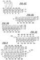
- Figure 1 illustrates in perspective view,a light influencing element ;
- Figures 2A-2C illustrate, in a partial cross-sectionalside view taken along line 2-2 of Figure 1,a method of fabricating the lightinfluencing element of Figure 1;
- Figures 3A-3C illustrate in cross-sectional,partial side view, the processing steps involved infabricating a liquid crystal display subassembly, fromthe light influencing element of Figures 1 and 2; and
- Figure 4 illustrates in cross-sectional, partialside view the processing steps required in order tofabricate a liquid crystal display from the liquidcrystal subassembly and light influencing element ofFigures 1, 2 and 3.
- Referring now to Figure 1, there isillustrated therein, in perspective view, a lightinfluencing element ,identified generally by the reference numeral 10. Thelight influencing element 10 will typically be employedas a color filter element, as is explained in greaterdetail hereinbelow, though it is to be understood thatsuch an element may be employed in a number ofdifferent applications including, but not limited to,a light diffuser, a light collimator, a light polarizeror a light rotating element. Alternatively, the lightinfluencing element may be adapted to provide anoptical effect upon radiation not in the range ofvisible light. Hence, said element may be adapted tofilter certain wavelengths of radiation such as infra-redor ultra-violet.
- The light influencing element 10 includes a
transparent substrate 12, which serves as the base uponwhich subsequent structures are formed. Thesubstantiallytransparent substrate 12, is typicallyfabricated from a device quality, high temperaturesheet of glass, which is free from defects and opticalinclusions. Alternatively, the substrate may be formedfrom other substantially transparent materials such asa clear plastic or other polymeric material which maybe either rigid, as glass, or flexible as would be the case for a thin, polymeric material such as a layer ofkapton, or polycarbonate materials of the type that arecurrently used in numerous applications whereinconsiderations such as hardness and optical clarity areof paramount importance. - Disposed upon said
substrate 12 is a layer ofsubstantiallyopaque material 14. The layer ofsubstantiallyopaque material 14 may typically beformed of a polymeric material such as a blackpolyimide material deposited to a thickness of between0.10 and 100.0 µm, and preferably between 1.0 and 10.0µm. Alternatively, the layer of substantiallyopaquematerial 14 may be formed of a metallic material, suchas, but not limited to, tin, chromium, molybdenum ortantalum deposited to a thickness sufficient tosubstantially prevent the transmission of lighttherethrough. The layer of substantiallyopaquematerial 14 may otherwise be formed from a layer of anon-metallic, and non-polymeric material, such as alayer of amorphous silicon or an amorphous siliconalloy material, again deposited to a thicknesssufficient to prevent the transmission of lighttherethrough. In one preferred embodiment, the layerof substantially opaque material is a layer of blackpolyimide material deposited to a depth of between 1.0and 10.0 µms. - Formed in said layer of substantially
opaquematerial 14 is at least oneopening 16 which extendsthrough saidlayer 14 to thesubstrate 12. The numberand spacing of the at least one opening, in the eventthat there are more than one, will depend upon theultimate application in which the light influencingelement is to be used employed. For example, if theelement 10 is to be used as a color filter in a liquidcrystal display, then the size, packing density, number and pitch of the picture elements (or pixels) of thedisplay will determine the size, packing density,number and pitch of theopenings 16 in the lightinfluencing element 10. Alternatively, the openingsmay be formed as one or more elongated strips in thelayer of substantially opaque material. - The
openings 16 themselves may be formed by anyone of a number of techniques, such as a conventionalphotolithographic and etch technique. In one preferredembodiment of the method of the instant invention,which is described in greater detail hereinbelow, theopenings 16 are formed by employing a high resolutioni.e., capable of at least micron scale resolution, highpower laser device, such as an excimer laser adapted tocut a plurality of similarly sized and shaped openingsin the layer of substantiallyopaque material 14. Theelement 10 of Figure 1 may be adapted, as mentionedabove to use in conjunction with a liquid crystaldisplay. Hence, the excimer laser should be able toform a plurality ofopenings 16 formed in a highlypacked N x M matrix of rows and columns. In Figure 1,the element 10 is arranged as a matrix of 3 x 3openings, though it is to be understood that theelement 10 may be arranged to include any number ofopenings arranged in rows and columns, or in any otherfashion, such as a series of interlocking triangles or"triads", or elongated stripes. - Disposed in each of the
openings 16 is a lightinfluencing material selected to provide a desiredoptical effect. For example, if the light influencingmaterial is to be employed as a color filter element,dye, ink such as the ink used in so-called ink-jettechnology or other color pigments may be disposed insaidopenings 16. The dyes or pigments, which may beeither of the additive or subtractive variety, would be disposed in a manner and to a thickness sufficient to,for example, color white light red as it passedtherethrough. Having appropriately prepared the lightinfluencing element 10 so as to provide a desiredoptical effect, the element 10 may then be adapted toserve as the foundation upon which an entire electronicoptical device, or some subassembly thereof, isfabricated. - Turning now to Figures 2A-2C, there is illustratedtherein, in a partial cross-sectional side view takenalong line 2-2 of Figure 1, a light influencing elementfabricated according to the instant invention. Moreparticularly, Figure 2A illustrates the
substrate 12,having a layer of substantiallyopaque material 14deposited on one surface thereof. As notedhereinabove, the substantiallyopaque material 14 maybe fabricated of a metal, semiconductor or a polymericmaterial, though in one preferred embodiment, the layerof substantiallyopaque material 14 is a layer of blackpolyimide material, deposited by, for example, spincoating or blade application, to a depth of between 1.0and 10.0 µm, so as to prevent the passage of lighttherethrough. - Referring now to Figure 2B, the
substrate 12 andlayer ofopaque material 14 are placed in relativelyclose proximity to and are exposed to a high power,high resolution laser device such as an excimer laser100. The high power, high resolution laser 100 isemployed to form, as by cutting, at least one openingin the layer ofopaque material 14. In Figure 2B, thelaser has formed six (6)openings layer 14. The excimer laser 100 must becapable of at least micron resolution, and thus shouldbe able to form a plurality of openings in a highlypacked N x M matrix of rows and columns. In Figure 1, the element 10 is arranged as a matrix of 3 x 3openings of which Figure 2 illustrates but six openingsin a row of 8, though it is to be understood that theelement 10 may be arranged to include any number ofopenings arranged in rows and columns, or in any otherfashion, such as triads or stripes. - In order to form more than one opening in thelayer of
opaque material 14, it is necessary to effectsome type of relative movement between the substrateand the laser. As the laser is capable of very highresolutions, the tolerances for any movement must bevery precise so as to not upset the resolution andpatterning of the openings. It is therefore necessaryto provide a precise raster-type or otherconventionally known step and repeat type device forscanning the laser across the surface of thesubstrate 12 andlayer 14. Alternatively, thesubstrate 12 andlayer 14 may be scanned across a stationary lasersource 100. - Turning now to Figure 2C, the
substrate 12 withthe layer ofopaque material 14 having a plurality ofopenings 16a-16f formed therein is placed in relativelyclose proximity to means for injecting a lightinfluencing material into said openings. Further, inone preferred embodiment of the invention, theseinjection means comprise three injection nozzles 21a,21b, and 21c which are adapted to inject, for example,dye, ink or color pigments into the openings 16a-16f,in so called "ink-jet" fashion. The nozzles 21a-21c orthesubstrate 12 may either be fitted with apparatus toeffect relative movement therebetween so that one ormore nozzles may be used to fill each opening. Hence,in the application wherein the light influencingelement 10 of Figure 1 is a color filter element havingred, green and blue filters, nozzle 21a may be adapted to inject red dye, ink or pigment into opening 16a tocreate red filter 18a, nozzle 21b may be adapted toinject blue dye, ink or pigment intoopening 16b tocreate blue filter 20a, and nozzle 21c may be adaptedto inject green dye, ink or pigment intoopening 16c tocreate green filter 22a. Thereafter, either thesubstrate 12 or the nozzles 21a-21c may be moved overto the nextunfilled openings 16d-16f, wherein nozzle21a injects red dye, ink or pigment into opening 16d tocreatered filter 18b, nozzle 21b injects blue dye, inkor pigment intoopening 16e to createblue filter 20b,and nozzle 21c injects green dye, ink or pigment intoopening 16f to creategreen filter 22b. This step andrepeat process is continued until all of the openingshave been filled. - The light influencing material disposed in eachopening can be any one of several materials which areinitially in a non-solid state, i.e, a liquid, anaqueous solution, a suspension, an emulsion or even arapidly condensing gas. The non-solid material willpossess the optical characteristics necessary toaccomplish a desired task such as polarization or colorfiltering of light passing therethrough. Moreover, thephysical characteristics of the material, such asviscosity, color coordinates, etc. are to be optimizedfor a desired application and performance when injectedin ink-jet fashion from nozzles 21a-21c. Preferredmaterials to be used in the openings of the lightinfluencing element 10, include ink, dyes or pigmentedinks, gelatins, organic materials and water solublematerials and such other materials that can be madesusceptible to injection as by ink-jet technology.
- After injecting said non-solid light influencingmaterials into said openings 16a-16f, it is necessaryto cure said injected materials to the solid state. This may be accomplished by any one of a number ofmeans ranging from allowing the materials to harden byexposure to ambient conditions, to placing thesubstrate and materials disposed thereon into an oven,such as an autoclave or infra-red oven, and exposingsaid materials to those conditions until cured to thesolid state. In this manner, it is possible tofabricate a light influencing element, such as a colorfilter for use in conjunction with a high resolutionliquid crystal display device, without encountering thelimitations of the prior art methods.
- A liquid crystal display subassembly may beobtained by employing the light influencing element 10of Figures 1 and 2. More particularly, Figures 3A-3Cillustrate in cross-sectional, partial side view, theprocessing steps involved in fabricating a liquidcrystal display subassembly, such as the so-calledpassive plate, from the light influencing element ofFigures 1 and 2. The subassembly, fully illustrated inFigure 3C as 300, is fabricated by disposing acontinuous layer of a transparent, passivating
material 26 atop thecolor filters black polyimide layer 14 of the lightinfluencing element 10 of Figures 1 and 2. Thepassivatingmaterial 26 is adapted to, and must bedeposited to a depth sufficient to perform at least twocritical functions: 1) to level the underlying filterand opaque layers to a continuous, flat surface toserve as a base upon which subsequent layers may beformed; 2) to electrically insulate the lightinfluencing element 10 from any electrically conductivelayers that may be disposed upon the passivating layer;and 3) to provide a flat, level surface so as to assurea uniform thickness for any layer of liquid crystalmaterial disposed thereon. As light must be able to pass through the element and subassembly, it isnecessary for thepassivating layer 26 to be formedfrom a layer of material that is also transparent. Inone preferred embodiment of the instant invention, thetransparent, insulating, passivatingmaterial 26 isformed from a transparent, organic material such as atransparent resin, SiNx, SiOx, polyimides andcombinations thereof. - Thereafter, a layer of a transparent, conductivematerial, such as a transparent
conductive oxidematerial 30 of Figure 3B, is disposed upon thepassivation layer 26. Preferred transparent conductiveoxides include indium oxide, tin oxide, indium tinoxide, cadmium sulfate and combinations thereof.Thereafter, employing photolithographic techniques wellknow in the art, the layer of transparentconductivematerial 30 is patterned to form a plurality ofelectrodes 32a-32f, which electrodes are formeddirectly above the openings 16a-16f, which definecolorfilters passivation layer 26.Alternatively, the layer of transparentconductivematerial 30 may be left unpatterned to achieve a so-calledcommon electrode. Accordingly, thesubassembly 300 would include a plurality of aligned color filtersand electrodes arranged in an N x M matrix array. Inthis way, it is possible to fabricate a liquid crystaldisplay subassembly which avoids the limitationsinherent in the prior art. - A liquid crystal display device may beobtained by employing the liquid crystal subassembly ofFigures 3A-3C. More particularly, Figure 4 illustratesin cross-sectional, partial side view the processingsteps required in order to fabricate a
liquid crystal display 400 from theliquid crystal subassembly 300 andlight influencing element 10 of the instant invention.Theliquid crystal subassembly 300 is employed tofabricate a liquid crystal display by providing asecond substrate 40, whichsubstrate 40 is typicallyfabricated from a device quality, high temperaturesheet of glass, which is free from defects and opticalinclusions. Alternatively, thesubstrate 40 may beformed from other substantially transparent materialssuch as a clear plastic or other polymeric materialwhich may be either rigid, as glass, or flexible aswould be the case for a thin, polymeric material suchas a layer of kapton, or polycarbonate materials of thetype that are currently used in numerous applicationswherein considerations such as hardness and opticalclarity are of paramount importance. - The
second substrate 40 has disposed thereupon alayer of transparent conductive material such as atransparentconductive oxide material 42. Preferredtransparent conductive oxides include indium oxide, tinoxide, indium tin oxide, cadmium sulfate andcombinations thereof. The layer of transparentconductive material 42 may be either a continuous layeror may be a patterned layer of display electrodesformed by conventional photolithographic processes.Thesecond substrate 40 may also have disposed thereonother micro-electronic devices such as transistors ordiodes which enhance the switching and otherperformance of the display. Thesecond substrate 40 isarranged so that the second layer of transparentconductive material 42 is spacedly disposed from andfacing the patterned layer of transparent conductivematerial disposed on thefirst substrate 12. A layerof liquid crystal material, such as a twisted nematic,cholesteric or other liquid crystal is disposed betweensaid first andsecond substrate - As may be readily appreciated by those skilled inthe art, the present invention can be practiced otherthan as is specifically disclosed herein. Thus, whilethe instant invention has been described with respectto certain preferred embodiments thereof, it is to beunderstood that the foregoing and other modificationsand variations may be made without departing from thescope thereof.
Claims (24)
- A method of fabricating a liquid crystal display, said method comprising thesteps of:providing a substantially transparent first substrate member (12);disposing a layer of substantially opaque material (14) upon one side ofsaid first substrate (12);forming at least three openings (16) through said layer of substantiallyopaque material (14);injecting a light influencing material including first, second, and third colors(18, 20, 22) in said at least three openings (16) directly on the first substrate (12),the first, second and third colors being injected substantially simultaneously in thethree openings, respectively;disposing a continuous layer of transparent, passivation material (26) atopsaid layer of opaque material and said light influencing material, the continuouslayer of transparent, passivation material (26) providing a substantially flat, levelsurface;disposing a layer of transparent, conductive material (30) atop saidsubstantially flat, level surface of the passivation layer (26);providing a second substantially transparent substrate member (40) havinga continuous layer of a transparent conductive material (42) disposed on onesurface thereof, said second substrate (40) being spacedly disposed from saidfirst substrate (12) and arranged so that the layer of transparent conductivematerial (42) of the second substrate (40) faces the layer of transparentconductive material (30) of the first substrate (12); anddisposing a layer of liquid crystal material between said first and secondsubstrates.
- The method according to claim 1, wherein at least one of the first andsecond transparent substrates (12; 40) includes a plastic material.
- The method according to claim 1, wherein the openings (16) are formedwithout using a photolithography process.
- The method according to claim 1, wherein the openings (16) are opticallyformed.
- The method according to claim 1, further including the step of selecting alight influencing material adapted to color white light.
- The method according to claim 5, wherein said light influencing material isadapted to color light into the group of colors consisting of red, green, blue, andcombinations thereof.
- A method of fabricating a liquid crystal display, said method comprising thesteps of:providing a substantially transparent first substrate member (12);disposing a layer of substantially opaque material (14) upon one side ofsaid first substrate (12);forming an opening (16) through said layer of substantially opaque material(14);injecting a light influencing material in said opening (16) directly on the firstsubstrate (12), the light influencing material filling the opening so as to prevent anyspill over of the light influencing material;disposing a continuous layer of transparent, passivation material (26) atopsaid layer of opaque material (14) and said light influencing material, thecontinuous layer of transparent, passivation material (26) providing a substantiallyflat, level surface;disposing a layer of transparent, conductive material (30) atop saidsubstantially flat, level surface of the passivation layer (26);providing a second substantially transparent substrate member (40) havinga continuous layer of a transparent conductive material (42) disposed on onesurface thereof, said second substrate (40) being spacedly disposed from saidfirst substrate (12) and arranged so that the layer of transparent conductivematerial (42) of the second substrate (40) faces the layer of transparentconductive material (30) of the first substrate (12); anddisposing a layer of liquid crystal material between said first and secondsubstrates.
- The method according to claim 7, wherein at least one of the first andsecond transparent substrates (12, 40) includes a plastic material.
- The method according to claim 7, wherein the openings (16) are formedwithout using a photolithography process.
- The method according to claim 7, wherein the openings (16) are opticallyformed.
- The method according to claim 7, further including the step of selecting alight influencing material adapted to color white light.
- The method according to claim 11, wherein said light influencing material isadapted to color light into the group of colors consisting of red, green, blue, andcombinations thereof.
- A method of fabricating a liquid crystal display, said method comprising thesteps of:wherein the method uses a high power laser process to form the opening inthe light influencing material.providing a substantially transparent first substrate member (12);disposing a layer of substantially opaque material (14) upon one side ofsaid first substrate (12);forming an opening (16) through said layer of substantially opaque material(14);injecting a light influencing material in said opening (16);disposing a layer of transparent, conductive material (30) over said lightinfluencing material;providing a second substantially transparent substrate member (40) havinga continuous layer of a transparent conductive material (42) disposed on onesurface thereof, said second substrate (40) being spacedly disposed from saidfirst substrate (12) and arranged so that the layer of transparent conductivematerial (42) of the second substrate (40) faces the layer of transparentconductive material (30) of the first substrate (12); anddisposing a layer of liquid crystal material between said first and secondsubstrates;
- The method according to claim 13, wherein at least one of the first andsecond transparent substrates (12, 40) includes a plastic material.
- The method according to claim 13, wherein the openings (16) are opticallyformed.
- The method according to claim 13, wherein the light influencing materialfills the opening (16) to a level less than a depth of the opening so as to preventany spill over of the light influencing material.
- The method according to claim 13, further including the step of selecting alight influencing material adapted to color white light.
- The method according to claim 17, wherein said light influencing material isadapted to color light into the group of colors consisting of red, green, blue, andcombinations thereof.
- A method of fabricating a liquid crystal display, said method comprising thesteps of:providing a substantially transparent first substrate member (12);disposing a layer of substantially opaque material (14) upon one side ofsaid first substrate (12);forming at least three openings (16) through said layer of substantiallyopaque material (14);injecting a light influencing material including first, second, and third colors(18, 20, 22) in said at least three openings (16) directly on the first substrate (12);disposing a continuous layer of transparent, passivation material (26) atopsaid layer of opaque material and said light influencing material, the continuouslayer of transparent, passivation material (26) providing a substantially flat, levelsurface; anddisposing a layer of transparent, conductive material (30) atop saidsubstantially flat, level surface of the passivation layer (26).
- The method according to claim 19, wherein the openings (16) are formedwithout using a photolithography process.
- The method according to claim 19, wherein the openings (16) are opticallyformed.
- The method according to claim 19, wherein the light influencing materialfills the opening to a level less than a depth of the opening (16) so as to preventany spill over of the light influencing material.
- The method according to claim 19, further including the step of selecting alight influencing material adapted to color white light.
- The method according to claim 23, wherein said light influencing material isadapted to color light into the group of colors consisting of red, green, blue, andcombinations thereof.
Applications Claiming Priority (4)
| Application Number | Priority Date | Filing Date | Title |
|---|---|---|---|
| US89085592A | 1992-06-01 | 1992-06-01 | |
| US890855 | 1992-06-01 | ||
| PCT/US1993/005174WO1993024240A1 (en) | 1992-06-01 | 1993-05-28 | Light influencing element for high resolution optical systems and method of making same |
| EP93914281AEP0605685B1 (en) | 1992-06-01 | 1993-05-28 | Light influencing element for high resolution optical systems and method of making same |
Related Parent Applications (1)
| Application Number | Title | Priority Date | Filing Date |
|---|---|---|---|
| EP93914281ADivisionEP0605685B1 (en) | 1992-06-01 | 1993-05-28 | Light influencing element for high resolution optical systems and method of making same |
Publications (3)
| Publication Number | Publication Date |
|---|---|
| EP0905544A2 EP0905544A2 (en) | 1999-03-31 |
| EP0905544A3 EP0905544A3 (en) | 1999-04-07 |
| EP0905544B1true EP0905544B1 (en) | 2003-05-21 |
Family
ID=25397227
Family Applications (2)
| Application Number | Title | Priority Date | Filing Date |
|---|---|---|---|
| EP98122876AExpired - LifetimeEP0905544B1 (en) | 1992-06-01 | 1993-05-28 | A method of fabricating a liquid crystal display |
| EP93914281AExpired - LifetimeEP0605685B1 (en) | 1992-06-01 | 1993-05-28 | Light influencing element for high resolution optical systems and method of making same |
Family Applications After (1)
| Application Number | Title | Priority Date | Filing Date |
|---|---|---|---|
| EP93914281AExpired - LifetimeEP0605685B1 (en) | 1992-06-01 | 1993-05-28 | Light influencing element for high resolution optical systems and method of making same |
Country Status (4)
| Country | Link |
|---|---|
| US (4) | US5281450A (en) |
| EP (2) | EP0905544B1 (en) |
| DE (2) | DE69326745T2 (en) |
| WO (1) | WO1993024240A1 (en) |
Families Citing this family (73)
| Publication number | Priority date | Publication date | Assignee | Title |
|---|---|---|---|---|
| KR940000143B1 (en)* | 1991-06-25 | 1994-01-07 | 재단법인 한국전자통신연구소 | Manufacturing method of large thin film transistor (TFT) liquid crystal display panel (LCD panel) |
| US5507323A (en)* | 1993-10-12 | 1996-04-16 | Fujitsu Limited | Method and dispenser for filling liquid crystal into LCD cell |
| JP3332515B2 (en)* | 1993-11-24 | 2002-10-07 | キヤノン株式会社 | Color filter, manufacturing method thereof, and liquid crystal panel |
| US6686104B1 (en) | 1993-11-24 | 2004-02-03 | Canon Kabushiki Kaisha | Color filter, method for manufacturing it, and liquid crystal panel |
| TW417034B (en)* | 1993-11-24 | 2001-01-01 | Canon Kk | Color filter, method for manufacturing it, and liquid crystal panel |
| JP2952143B2 (en)* | 1993-12-21 | 1999-09-20 | キヤノン株式会社 | Manufacturing method of color filter |
| DE69523351T2 (en) | 1994-01-28 | 2002-05-02 | Canon K.K., Tokio/Tokyo | Color filters, process for their manufacture, and liquid crystal panel |
| JP2839133B2 (en)* | 1994-03-31 | 1998-12-16 | キヤノン株式会社 | Method and apparatus for manufacturing color filter, method for manufacturing liquid crystal display, and method for manufacturing apparatus equipped with liquid crystal display |
| JP3034438B2 (en)* | 1994-03-31 | 2000-04-17 | キヤノン株式会社 | Color filter manufacturing equipment |
| EP0683405A1 (en)* | 1994-05-18 | 1995-11-22 | Xerox Corporation | Acoustic fabrication of color filters |
| JP2839134B2 (en)* | 1994-05-20 | 1998-12-16 | キヤノン株式会社 | Method of manufacturing color filter, method of manufacturing liquid crystal display device, method of manufacturing device having liquid crystal display device, and method of reducing color mixture between adjacent colored portions of color filter |
| JP3376169B2 (en)* | 1994-06-17 | 2003-02-10 | キヤノン株式会社 | Color filter manufacturing method and color filter manufactured by the method |
| JP3014923B2 (en)* | 1994-06-24 | 2000-02-28 | キヤノン株式会社 | Color filter, method of manufacturing the same, and liquid crystal display using the filter |
| JP3372671B2 (en)* | 1994-09-14 | 2003-02-04 | キヤノン株式会社 | Method and apparatus for manufacturing color filter |
| JPH08146214A (en)* | 1994-09-19 | 1996-06-07 | Canon Inc | Color filter manufacturing method, color filter, liquid crystal panel, and information processing apparatus including the liquid crystal panel |
| JP3372724B2 (en)* | 1994-09-21 | 2003-02-04 | キヤノン株式会社 | Color filter and manufacturing method thereof, liquid crystal panel, and information processing device |
| JPH08227011A (en)* | 1994-09-30 | 1996-09-03 | Canon Inc | Color filter, manufacturing method thereof, liquid crystal panel, and information processing apparatus including the same |
| DE69629864T2 (en)* | 1995-04-03 | 2004-07-15 | Canon K.K. | Method of manufacturing an electron emitting device, an electron source and an image forming apparatus |
| US5984470A (en)* | 1995-04-20 | 1999-11-16 | Canon Kabushiki Kaisha | Apparatus for producing color filter with alignment error detection |
| US5609943A (en)* | 1995-06-02 | 1997-03-11 | The Dow Chemical Company | Non-wettable layer for color filters in flat panel display devices |
| JP3111024B2 (en)* | 1995-07-19 | 2000-11-20 | キヤノン株式会社 | Apparatus and method for manufacturing color filter, method for manufacturing display apparatus, and method for manufacturing apparatus provided with display apparatus |
| JP3124722B2 (en)* | 1995-07-31 | 2001-01-15 | キヤノン株式会社 | Method and apparatus for manufacturing color filter, method of reducing color mixture between partitioned areas of color filter, method of improving accuracy of ink application position to partitioned area of color filter, and coloring unevenness of partitioned area of color filter Reduction method |
| JP3159919B2 (en)* | 1995-08-01 | 2001-04-23 | キヤノン株式会社 | Apparatus and method for manufacturing color filter and method for reducing uneven coloring |
| JP3113797B2 (en)* | 1995-08-28 | 2000-12-04 | インターナショナル・ビジネス・マシーンズ・コーポレ−ション | Method for modifying photosensitive chemical film |
| JP3234854B2 (en)* | 1995-08-28 | 2001-12-04 | アルプス電気株式会社 | Multilayer filter and manufacturing method thereof |
| JPH09292633A (en)* | 1996-02-27 | 1997-11-11 | Canon Inc | Method for manufacturing color liquid crystal display device |
| KR100479000B1 (en)* | 1996-05-15 | 2005-08-01 | 세이코 엡슨 가부시키가이샤 | Manufacturing method of thin film device, liquid crystal panel and electronic device and thin film device |
| US5824374A (en)* | 1996-07-22 | 1998-10-20 | Optical Coating Laboratory, Inc. | In-situ laser patterning of thin film layers during sequential depositing |
| CN100485904C (en)* | 1996-09-19 | 2009-05-06 | 精工爱普生株式会社 | Matrix type display device and manufacturing method thereof |
| US20020075422A1 (en)* | 1996-09-19 | 2002-06-20 | Seiko Epson Corporation | Matrix type display device and manufacturing method thereof |
| JP3115549B2 (en)* | 1996-09-30 | 2000-12-11 | キヤノン株式会社 | INK JET RECORDING APPARATUS, RECORDING METHOD, ASSISTANT MEMBER, INK JET HEAD, AND WARP CONTROL METHOD |
| JP2978459B2 (en)* | 1996-09-30 | 1999-11-15 | キヤノン株式会社 | Method and apparatus for manufacturing color filter, color filter, display apparatus, and apparatus having display apparatus |
| DE69735689T2 (en)* | 1996-10-30 | 2007-04-26 | Seiko Epson Corporation, Shinjuku | color filter |
| JP3899566B2 (en) | 1996-11-25 | 2007-03-28 | セイコーエプソン株式会社 | Manufacturing method of organic EL display device |
| US5912056A (en)* | 1997-03-31 | 1999-06-15 | Candescent Technologies Corporation | Black matrix with conductive coating |
| US6816218B1 (en)* | 1997-04-14 | 2004-11-09 | Merck Patent Gmbh | Homeotropically aligned liquid crystal layer and process for the homeotropic alignment of liquid crystals on plastic substrates |
| JPH112716A (en) | 1997-06-13 | 1999-01-06 | Canon Inc | Color filter, liquid crystal element using the same, manufacturing method thereof, and inkjet ink used in the manufacturing method |
| JPH11183882A (en)* | 1997-12-18 | 1999-07-09 | Nikon Corp | Manufacturing method of liquid crystal display element |
| US7663607B2 (en) | 2004-05-06 | 2010-02-16 | Apple Inc. | Multipoint touchscreen |
| KR100282393B1 (en)* | 1998-06-17 | 2001-02-15 | 구자홍 | method for fabricating Organic Electroluminescent display Device |
| US6262789B1 (en)* | 1998-11-27 | 2001-07-17 | Zvi Yaniv | Liquid display and method of making same |
| US7014521B1 (en) | 1999-08-05 | 2006-03-21 | Canon Kabushiki Kaisha | Display panel having a color filter and a protective layer of heat melted material and method of manufacturing the display panel |
| TW468283B (en) | 1999-10-12 | 2001-12-11 | Semiconductor Energy Lab | EL display device and a method of manufacturing the same |
| KR100675087B1 (en)* | 2000-12-28 | 2007-01-26 | 엘지.필립스 엘시디 주식회사 | Cholesteric Liquid Crystal Color Filter |
| GB2397423B (en)* | 2001-09-17 | 2005-06-01 | Ca Minister Agriculture & Food | A method and apparatus for identifying and quantifying characteristics of seeds and other small objects |
| US7553390B2 (en)* | 2001-11-08 | 2009-06-30 | Sharp Kabushiki Kaisha | Method and device for parting glass substrate, liquid crystal panel, and liquid crystal panel manufacturing device |
| JP2003288030A (en)* | 2002-03-27 | 2003-10-10 | Seiko Epson Corp | Electro-optical device, method and device for manufacturing the same, and electronic apparatus |
| JP4200810B2 (en)* | 2002-05-17 | 2008-12-24 | セイコーエプソン株式会社 | Display manufacturing apparatus and display manufacturing method |
| US7514149B2 (en)* | 2003-04-04 | 2009-04-07 | Corning Incorporated | High-strength laminated sheet for optical applications |
| JP2005062307A (en)* | 2003-08-08 | 2005-03-10 | Fujitsu Hitachi Plasma Display Ltd | Method for manufacturing flat-panel display |
| EP1728120B1 (en) | 2004-03-20 | 2014-06-04 | Hewlett-Packard Development Company, L.P. | Applying colour elements and busbars to a display substrate |
| US7483732B2 (en)* | 2004-04-15 | 2009-01-27 | Boston Scientific Scimed, Inc. | Magnetic resonance imaging of a medical device and proximate body tissue |
| US20060092218A1 (en)* | 2004-11-04 | 2006-05-04 | Applied Materials, Inc. | Methods and apparatus for inkjet printing |
| US7625063B2 (en) | 2004-11-04 | 2009-12-01 | Applied Materials, Inc. | Apparatus and methods for an inkjet head support having an inkjet head capable of independent lateral movement |
| US20070065571A1 (en)* | 2005-09-19 | 2007-03-22 | Applied Materials. Inc. | Method and apparatus for manufacturing a pixel matrix of a color filter for a flat panel display |
| US20080043318A1 (en)* | 2005-10-18 | 2008-02-21 | E Ink Corporation | Color electro-optic displays, and processes for the production thereof |
| CN100529807C (en)* | 2005-12-30 | 2009-08-19 | 鸿富锦精密工业(深圳)有限公司 | Method for manufacturing polarizer |
| US8094271B2 (en)* | 2006-02-03 | 2012-01-10 | Fujifilm Corporation | Liquid crystal display device and color film plate, and processes for producing the same |
| CN104965621B (en) | 2006-06-09 | 2018-06-12 | 苹果公司 | Touch screen LCD and its operating method |
| CN102981678B (en) | 2006-06-09 | 2015-07-22 | 苹果公司 | Touch screen liquid crystal display |
| US8259078B2 (en) | 2006-06-09 | 2012-09-04 | Apple Inc. | Touch screen liquid crystal display |
| US20080026302A1 (en)* | 2006-07-28 | 2008-01-31 | Quanyuan Shang | Black matrix compositions and methods of forming the same |
| US7932972B2 (en) | 2006-10-02 | 2011-04-26 | Lg Display Co., Ltd. | Substrate for liquid crystal display device and method of fabricating the same |
| US8493330B2 (en) | 2007-01-03 | 2013-07-23 | Apple Inc. | Individual channel phase delay scheme |
| US9710095B2 (en) | 2007-01-05 | 2017-07-18 | Apple Inc. | Touch screen stack-ups |
| US20090141218A1 (en)* | 2007-10-26 | 2009-06-04 | Applied Materials, Inc. | Methods and apparatus for curing pixel matrix filter materials |
| WO2009055621A1 (en)* | 2007-10-26 | 2009-04-30 | Applied Materials, Inc. | Methods and apparatus for forming color filter on array flat panel displays |
| KR101735812B1 (en)* | 2010-09-10 | 2017-05-16 | 삼성디스플레이 주식회사 | Display apparatus |
| US8804056B2 (en) | 2010-12-22 | 2014-08-12 | Apple Inc. | Integrated touch screens |
| WO2013112990A1 (en)* | 2012-01-27 | 2013-08-01 | Applied Nanotech Holdings, Inc. | Display medium and color reflective inks |
| DE102015000699A1 (en) | 2015-01-20 | 2016-07-21 | Technische Universität Ilmenau | Device and method for automatic sorting of bulk material |
| US20170112371A1 (en)* | 2015-10-27 | 2017-04-27 | George Percy McGown | Anoscope |
| US10301232B2 (en) | 2016-07-28 | 2019-05-28 | Honeywell International Inc. | Propellant and self-protection compositions |
Family Cites Families (52)
| Publication number | Priority date | Publication date | Assignee | Title |
|---|---|---|---|---|
| CA1127227A (en)* | 1977-10-03 | 1982-07-06 | Ichiro Endo | Liquid jet recording process and apparatus therefor |
| JPS5936879B2 (en)* | 1977-10-14 | 1984-09-06 | キヤノン株式会社 | Thermal transfer recording medium |
| US4330787A (en)* | 1978-10-31 | 1982-05-18 | Canon Kabushiki Kaisha | Liquid jet recording device |
| US4345262A (en)* | 1979-02-19 | 1982-08-17 | Canon Kabushiki Kaisha | Ink jet recording method |
| US4463359A (en)* | 1979-04-02 | 1984-07-31 | Canon Kabushiki Kaisha | Droplet generating method and apparatus thereof |
| US4313124A (en)* | 1979-05-18 | 1982-01-26 | Canon Kabushiki Kaisha | Liquid jet recording process and liquid jet recording head |
| US4388128A (en)* | 1980-03-17 | 1983-06-14 | Matsushita Electric Industrial Co., Ltd. | Solid-state color-image sensor and process for fabricating the same |
| US4558333A (en)* | 1981-07-09 | 1985-12-10 | Canon Kabushiki Kaisha | Liquid jet recording head |
| JPS5975205A (en)* | 1982-10-25 | 1984-04-27 | Seiko Epson Corp | Color filter manufacturing method |
| JPS5984206A (en)* | 1982-11-08 | 1984-05-15 | Seiko Epson Corp | color filter |
| JPS59123670A (en)* | 1982-12-28 | 1984-07-17 | Canon Inc | Ink jet head |
| JPS59138461A (en)* | 1983-01-28 | 1984-08-08 | Canon Inc | liquid jet recording device |
| US4698113A (en)* | 1983-08-11 | 1987-10-06 | Matsushita Electric | Method of curing photocurable and heat-curable compositions and a method of adhering members to each other by using them |
| JPS6071260A (en)* | 1983-09-28 | 1985-04-23 | Erumu:Kk | Recorder |
| JPS613122A (en)* | 1984-06-15 | 1986-01-09 | Sony Corp | Production of liquid crystal color display element |
| JPS6177014A (en)* | 1984-09-25 | 1986-04-19 | Seikosha Co Ltd | Manufacture of color filter |
| JPS61245106A (en)* | 1985-04-23 | 1986-10-31 | Seiko Epson Corp | Color filter manufacturing method |
| JPS62109002A (en)* | 1985-11-07 | 1987-05-20 | Matsushita Electric Ind Co Ltd | Manufacturing method of color filter for liquid crystal display |
| US4864324A (en)* | 1986-08-13 | 1989-09-05 | Canon Kabushiki Kaisha | Color image forming method and ink used therefor |
| US4995705A (en)* | 1986-12-17 | 1991-02-26 | Canon Kabushiki Kaisha | Device, method and apparatus for optical modulation using ferroelectric polymer liquid crystals |
| JP2739315B2 (en)* | 1987-01-23 | 1998-04-15 | キヤノン株式会社 | Color filters and color liquid crystal devices |
| JPS63205608A (en)* | 1987-02-23 | 1988-08-25 | Matsushita Electric Ind Co Ltd | Manufacturing method of color filter for liquid crystal display |
| JPS63205607A (en)* | 1987-02-23 | 1988-08-25 | Matsushita Electric Ind Co Ltd | Manufacturing method of color filter for liquid crystal display |
| JPS63235901A (en)* | 1987-03-24 | 1988-09-30 | Fujitsu Ltd | How to form a color filter |
| JPH0721562B2 (en)* | 1987-05-14 | 1995-03-08 | 凸版印刷株式会社 | Color filter |
| JPS63294503A (en)* | 1987-05-27 | 1988-12-01 | Fujitsu Ltd | Color filter manufacturing method |
| JP2637469B2 (en)* | 1987-06-04 | 1997-08-06 | キヤノン株式会社 | Polymer liquid crystal device |
| US4981614A (en)* | 1987-09-21 | 1991-01-01 | Canon Kabushiki Kaisha | Solid solution |
| JPH01102504A (en)* | 1987-10-16 | 1989-04-20 | Toshiba Corp | Color filter manufacturing method |
| JP2597626B2 (en)* | 1988-02-26 | 1997-04-09 | 株式会社東芝 | Color filter substrate, method of manufacturing color filter substrate, and liquid crystal display device using color filter substrate |
| JPH01235903A (en)* | 1988-03-16 | 1989-09-20 | Matsushita Electric Ind Co Ltd | Color filter manufacturing method |
| US5011623A (en)* | 1988-07-20 | 1991-04-30 | Canon Kabushiki Kaisha | Nonlinear optical material and nonlinear optical device |
| ATE107235T1 (en)* | 1988-11-02 | 1994-07-15 | Canon Kk | INKJET RECORDING SYSTEM AND RECORDING METHOD USING THE SAME. |
| EP0368260B1 (en)* | 1988-11-10 | 1995-01-18 | Kabushiki Kaisha Toshiba | Liquid crystal display device and color filter for use with the liquid crystal display device and method of making the color filter |
| JPH02156202A (en)* | 1988-12-08 | 1990-06-15 | Dainippon Toryo Co Ltd | Color filter manufacturing method |
| JPH02173703A (en)* | 1988-12-27 | 1990-07-05 | Seiko Epson Corp | Color filter manufacturing method |
| JPH02173704A (en)* | 1988-12-27 | 1990-07-05 | Seiko Epson Corp | Manufacture of color filter |
| JPH02228605A (en)* | 1989-02-28 | 1990-09-11 | Fujitsu Ltd | Color filter manufacturing method |
| JPH02287427A (en)* | 1989-04-28 | 1990-11-27 | Seiko Epson Corp | Integrated structure of liquid crystal panel and solar cell |
| JPH0310220A (en)* | 1989-06-07 | 1991-01-17 | Fujitsu Ltd | liquid crystal display device |
| JPH03280002A (en)* | 1990-03-29 | 1991-12-11 | Toppan Printing Co Ltd | Color filter |
| JP2537562B2 (en)* | 1990-05-28 | 1996-09-25 | シャープ株式会社 | Method for manufacturing color filter layer of liquid crystal display device |
| WO1991020006A1 (en)* | 1990-06-20 | 1991-12-26 | Dai Nippon Printing Co., Ltd. | Color filter and method of manufacturing the same |
| JP3172167B2 (en)* | 1990-07-12 | 2001-06-04 | セイコーエプソン株式会社 | Electro-optical device and method of manufacturing electro-optical device |
| JPH0470803A (en)* | 1990-07-12 | 1992-03-05 | Toshiba Corp | Method for manufacturing color filters for liquid crystal display devices |
| JPH0486801A (en)* | 1990-07-31 | 1992-03-19 | Toshiba Corp | Production of color filter |
| JP3103094B2 (en)* | 1990-08-27 | 2000-10-23 | 共同印刷株式会社 | Pattern member forming method and apparatus used therefor |
| JPH04123005A (en)* | 1990-09-14 | 1992-04-23 | Toray Ind Inc | Production of color filter |
| JPH04123007A (en)* | 1990-09-14 | 1992-04-23 | Toray Ind Inc | Production of color filter |
| JP2946700B2 (en)* | 1990-09-14 | 1999-09-06 | 東レ株式会社 | Manufacturing method of color filter for liquid crystal display |
| US5079214A (en)* | 1990-10-11 | 1992-01-07 | Eastman Kodak Company | Patterned receiver for color filter array |
| JPH04156402A (en)* | 1990-10-19 | 1992-05-28 | Dainippon Printing Co Ltd | Color filter |
- 1993
- 1993-05-28EPEP98122876Apatent/EP0905544B1/ennot_activeExpired - Lifetime
- 1993-05-28EPEP93914281Apatent/EP0605685B1/ennot_activeExpired - Lifetime
- 1993-05-28DEDE69326745Tpatent/DE69326745T2/ennot_activeExpired - Lifetime
- 1993-05-28WOPCT/US1993/005174patent/WO1993024240A1/enactiveIP Right Grant
- 1993-05-28DEDE69333000Tpatent/DE69333000T2/ennot_activeExpired - Lifetime
- 1993-05-28USUS08/068,305patent/US5281450A/ennot_activeExpired - Lifetime
- 1993-11-12USUS08/150,788patent/US5576070A/ennot_activeCeased
- 1998
- 1998-11-18USUS09/195,076patent/USRE36711E/ennot_activeExpired - Lifetime
- 1999
- 1999-11-16USUS09/441,139patent/USRE37682E1/ennot_activeExpired - Lifetime
Also Published As
| Publication number | Publication date |
|---|---|
| USRE36711E (en) | 2000-05-23 |
| EP0605685A4 (en) | 1994-11-02 |
| WO1993024240A1 (en) | 1993-12-09 |
| DE69333000D1 (en) | 2003-06-26 |
| USRE37682E1 (en) | 2002-04-30 |
| DE69326745D1 (en) | 1999-11-18 |
| EP0905544A2 (en) | 1999-03-31 |
| EP0605685A1 (en) | 1994-07-13 |
| DE69333000T2 (en) | 2004-02-19 |
| US5576070A (en) | 1996-11-19 |
| EP0905544A3 (en) | 1999-04-07 |
| US5281450A (en) | 1994-01-25 |
| EP0605685B1 (en) | 1999-10-13 |
| DE69326745T2 (en) | 2000-04-27 |
Similar Documents
| Publication | Publication Date | Title |
|---|---|---|
| EP0905544B1 (en) | A method of fabricating a liquid crystal display | |
| US4776675A (en) | Multicolor liquid crystal display device having printed color filters | |
| KR100808466B1 (en) | Array substrate for liquid crystal display device and manufacturing method thereof | |
| US5473453A (en) | Liquid crystal display with opaque film formed by exposure through microlens | |
| US4597637A (en) | Color optical printer head having a liquid crystal layer | |
| KR0171230B1 (en) | Manufacturing Method of Liquid Crystal Display | |
| KR100661291B1 (en) | Color filter substrate and its manufacturing method. | |
| US4935757A (en) | Liquid crystal display device | |
| US20110181819A1 (en) | Liquid crystal display and method for manufacturing the same | |
| CA2352168C (en) | Color filters for flat panel displays | |
| KR930010664B1 (en) | Method of manufacturing liquid crystal display device | |
| KR100308092B1 (en) | Liquid crystal display and manufacturing method thereof | |
| JPH0980221A (en) | Color filter substrate for liquid crystal display device and manufacturing method thereof | |
| KR940004297B1 (en) | Method of making color filter of liquid crystal display | |
| JPH0486809A (en) | Liquid crystal display device | |
| KR100790354B1 (en) | Manufacturing method of color filter substrate and array substrate for liquid crystal display | |
| US6203950B1 (en) | Method for manufacturing a color filter | |
| KR100749458B1 (en) | LCD with color filter formed on TF array and its manufacturing method | |
| US20070211196A1 (en) | Color filter panel and manufacturing method thereof | |
| KR960009378Y1 (en) | Color filter base plate for liquid crystal display | |
| JPH01102504A (en) | Color filter manufacturing method | |
| KR960016636B1 (en) | Manufacturing method of color filter for liquid crystal display element | |
| JP2745544B2 (en) | Manufacturing method of TFT type liquid crystal display device | |
| KR19980054985A (en) | Substrate for liquid crystal display and manufacturing method | |
| KR19990070839A (en) | Color filter substrate and its manufacturing method |
Legal Events
| Date | Code | Title | Description |
|---|---|---|---|
| PUAI | Public reference made under article 153(3) epc to a published international application that has entered the european phase | Free format text:ORIGINAL CODE: 0009012 | |
| PUAL | Search report despatched | Free format text:ORIGINAL CODE: 0009013 | |
| 17P | Request for examination filed | Effective date:19981202 | |
| AC | Divisional application: reference to earlier application | Ref document number:605685 Country of ref document:EP | |
| AK | Designated contracting states | Kind code of ref document:A2 Designated state(s):DE FR GB IT NL | |
| AK | Designated contracting states | Kind code of ref document:A3 Designated state(s):DE FR GB IT NL | |
| RIN1 | Information on inventor provided before grant (corrected) | Inventor name:YANIV, ZVI | |
| 17Q | First examination report despatched | Effective date:20000920 | |
| GRAG | Despatch of communication of intention to grant | Free format text:ORIGINAL CODE: EPIDOS AGRA | |
| GRAG | Despatch of communication of intention to grant | Free format text:ORIGINAL CODE: EPIDOS AGRA | |
| GRAH | Despatch of communication of intention to grant a patent | Free format text:ORIGINAL CODE: EPIDOS IGRA | |
| RAP1 | Party data changed (applicant data changed or rights of an application transferred) | Owner name:LG.PHILIPS LCD CO., LTD. | |
| GRAH | Despatch of communication of intention to grant a patent | Free format text:ORIGINAL CODE: EPIDOS IGRA | |
| GRAA | (expected) grant | Free format text:ORIGINAL CODE: 0009210 | |
| AC | Divisional application: reference to earlier application | Ref document number:0605685 Country of ref document:EP Kind code of ref document:P | |
| AK | Designated contracting states | Designated state(s):DE FR GB IT NL | |
| REG | Reference to a national code | Ref country code:GB Ref legal event code:FG4D | |
| REF | Corresponds to: | Ref document number:69333000 Country of ref document:DE Date of ref document:20030626 Kind code of ref document:P | |
| ET | Fr: translation filed | ||
| PLBE | No opposition filed within time limit | Free format text:ORIGINAL CODE: 0009261 | |
| STAA | Information on the status of an ep patent application or granted ep patent | Free format text:STATUS: NO OPPOSITION FILED WITHIN TIME LIMIT | |
| 26N | No opposition filed | Effective date:20040224 | |
| PGFP | Annual fee paid to national office [announced via postgrant information from national office to epo] | Ref country code:DE Payment date:20120531 Year of fee payment:20 Ref country code:NL Payment date:20120605 Year of fee payment:20 | |
| PGFP | Annual fee paid to national office [announced via postgrant information from national office to epo] | Ref country code:GB Payment date:20120612 Year of fee payment:20 Ref country code:FR Payment date:20120625 Year of fee payment:20 | |
| PGFP | Annual fee paid to national office [announced via postgrant information from national office to epo] | Ref country code:IT Payment date:20120531 Year of fee payment:20 | |
| REG | Reference to a national code | Ref country code:DE Ref legal event code:R071 Ref document number:69333000 Country of ref document:DE | |
| REG | Reference to a national code | Ref country code:NL Ref legal event code:V4 Effective date:20130528 | |
| REG | Reference to a national code | Ref country code:GB Ref legal event code:PE20 Expiry date:20130527 | |
| PG25 | Lapsed in a contracting state [announced via postgrant information from national office to epo] | Ref country code:DE Free format text:LAPSE BECAUSE OF EXPIRATION OF PROTECTION Effective date:20130529 Ref country code:GB Free format text:LAPSE BECAUSE OF EXPIRATION OF PROTECTION Effective date:20130527 |