EP0903605B1 - Four mirror EUV projection optics - Google Patents
Four mirror EUV projection opticsDownload PDFInfo
- Publication number
- EP0903605B1 EP0903605B1EP98117168AEP98117168AEP0903605B1EP 0903605 B1EP0903605 B1EP 0903605B1EP 98117168 AEP98117168 AEP 98117168AEP 98117168 AEP98117168 AEP 98117168AEP 0903605 B1EP0903605 B1EP 0903605B1
- Authority
- EP
- European Patent Office
- Prior art keywords
- mirror
- concave mirror
- convex mirror
- convex
- conjugate end
- Prior art date
- Legal status (The legal status is an assumption and is not a legal conclusion. Google has not performed a legal analysis and makes no representation as to the accuracy of the status listed.)
- Expired - Lifetime
Links
- 230000003287optical effectEffects0.000claimsdescription58
- 230000005670electromagnetic radiationEffects0.000claimsdescription29
- 238000010276constructionMethods0.000claimsdescription4
- 238000004519manufacturing processMethods0.000claimsdescription4
- 239000004065semiconductorSubstances0.000claimsdescription4
- 239000011521glassSubstances0.000claimsdescription2
- 238000005286illuminationMethods0.000description11
- 230000008901benefitEffects0.000description5
- 230000004075alterationEffects0.000description4
- 238000001459lithographyMethods0.000description4
- 238000000206photolithographyMethods0.000description4
- 238000001393microlithographyMethods0.000description3
- 241000276498Pollachius virensSpecies0.000description2
- 239000000758substrateSubstances0.000description2
- 230000000903blocking effectEffects0.000description1
- 238000000576coating methodMethods0.000description1
- 238000010586diagramMethods0.000description1
- 238000005516engineering processMethods0.000description1
- 238000003384imaging methodMethods0.000description1
- 238000000034methodMethods0.000description1
- 238000012986modificationMethods0.000description1
- 230000004048modificationEffects0.000description1
- 230000005855radiationEffects0.000description1
Images

Classifications
- G—PHYSICS
- G03—PHOTOGRAPHY; CINEMATOGRAPHY; ANALOGOUS TECHNIQUES USING WAVES OTHER THAN OPTICAL WAVES; ELECTROGRAPHY; HOLOGRAPHY
- G03F—PHOTOMECHANICAL PRODUCTION OF TEXTURED OR PATTERNED SURFACES, e.g. FOR PRINTING, FOR PROCESSING OF SEMICONDUCTOR DEVICES; MATERIALS THEREFOR; ORIGINALS THEREFOR; APPARATUS SPECIALLY ADAPTED THEREFOR
- G03F7/00—Photomechanical, e.g. photolithographic, production of textured or patterned surfaces, e.g. printing surfaces; Materials therefor, e.g. comprising photoresists; Apparatus specially adapted therefor
- G03F7/70—Microphotolithographic exposure; Apparatus therefor
- G03F7/70216—Mask projection systems
- G03F7/70233—Optical aspects of catoptric systems, i.e. comprising only reflective elements, e.g. extreme ultraviolet [EUV] projection systems
- G—PHYSICS
- G02—OPTICS
- G02B—OPTICAL ELEMENTS, SYSTEMS OR APPARATUS
- G02B13/00—Optical objectives specially designed for the purposes specified below
- G02B13/14—Optical objectives specially designed for the purposes specified below for use with infrared or ultraviolet radiation
- G02B13/143—Optical objectives specially designed for the purposes specified below for use with infrared or ultraviolet radiation for use with ultraviolet radiation
- G—PHYSICS
- G02—OPTICS
- G02B—OPTICAL ELEMENTS, SYSTEMS OR APPARATUS
- G02B17/00—Systems with reflecting surfaces, with or without refracting elements
- G02B17/02—Catoptric systems, e.g. image erecting and reversing system
- G02B17/06—Catoptric systems, e.g. image erecting and reversing system using mirrors only, i.e. having only one curved mirror
- G02B17/0647—Catoptric systems, e.g. image erecting and reversing system using mirrors only, i.e. having only one curved mirror using more than three curved mirrors
- G02B17/0657—Catoptric systems, e.g. image erecting and reversing system using mirrors only, i.e. having only one curved mirror using more than three curved mirrors off-axis or unobscured systems in which all of the mirrors share a common axis of rotational symmetry
- G—PHYSICS
- G03—PHOTOGRAPHY; CINEMATOGRAPHY; ANALOGOUS TECHNIQUES USING WAVES OTHER THAN OPTICAL WAVES; ELECTROGRAPHY; HOLOGRAPHY
- G03F—PHOTOMECHANICAL PRODUCTION OF TEXTURED OR PATTERNED SURFACES, e.g. FOR PRINTING, FOR PROCESSING OF SEMICONDUCTOR DEVICES; MATERIALS THEREFOR; ORIGINALS THEREFOR; APPARATUS SPECIALLY ADAPTED THEREFOR
- G03F7/00—Photomechanical, e.g. photolithographic, production of textured or patterned surfaces, e.g. printing surfaces; Materials therefor, e.g. comprising photoresists; Apparatus specially adapted therefor
- G03F7/70—Microphotolithographic exposure; Apparatus therefor
- G03F7/70216—Mask projection systems
- G03F7/70358—Scanning exposure, i.e. relative movement of patterned beam and workpiece during imaging
Definitions
- the present inventionrelates in general to semiconductor manufacturing using photolithography or microlithography, and more particularly to an optical projection system for use in the extreme ultraviolet wavelength region, for example from 11 to 13 nm.
- Semiconductor devicesare typically manufactured by projecting an image of a reticle containing a circuit pattern onto a photosensitive resist covered wafer.
- a photosensitive resist covered waferAs the feature size of the circuit elements become smaller, there is a need for the use of smaller or shorter wavelengths of light or electromagnetic radiation use in exposing the photosensitive resist covered wafer.
- One such optical projection systemis disclosed in U.S. Patent 5,353,322 entitled "Lens Systems For X-Ray Projection Lithography Camera" issuing to Bruning et al on October 4, 1994.
- a three mirror projection systemused in lithography at X-ray wavelengths to image a mask on a wafer. Also disclosed is a methodology for providing optimum solutions within regions of two dimensional magnification space defined by the magnification of a convex mirror as one coordinate and the ratio of the magnification of a pair of concave mirrors optically on opposite sides of the convex mirror as another coordinate.
- An optical systemis discloses having, from the image to the object end, a concave mirror, a convex mirror, and a concave mirror.
- Bruning et alspecifically advocates the use of a three-mirror system as opposed to other two and four mirror systems.
- Tanya E. Jewelldescribes in "The Journal of Vacuum Science and Technology” B, 8 (1990) Nov/Dec, No. 6, pp. 1519-1523, a four mirror anastigmat as a reflective system for soft x-ray projection lithography in a reflective systems design study.
- US Patent No. 5,410,434describes a reflective projection system with a relatively wide field of view that comprises two concave and two convex spherical mirrors situated in certain non-light blocking positions with respect to one another for deriving, with negligible image aberrations, a projected magnified or demagnified image.
- the present inventionrelates to an all reflecting ring field projection optical system designed for use with wavelengths in the extreme ultraviolet, including wavelengths in the 11 to 13 nm range, or soft X-rays.
- the present inventioncomprises a plurality of curved mirrors providing a reduction from a long conjugate end to a short conjugate end.
- the mirror order or sequence from the long conjugate end to the short conjugate endis a first negative power convex mirror, a first positive power concave mirror, a second negative convex mirror, and a second positive concave mirror.
- the plurality of curved mirrorsare arranged such that an aperture stop is coincident at or near the third mirror or second negative convex mirror.
- the reflective surfaces of each mirrorare spaced or separated by a distance greater than twenty-five percent of the total distance between the long conjugate end and the short conjugate end.
- variable irismay be utilized at the aperture stop.
- the object and image positionsare located or positioned to facilitate scanning.
- the first mirror from the long conjugate end to the short conjugate endis a negative power convex mirror.
- the mirrorsare spaced relatively far apart to minimize the angular variations of light beams hitting the mirrors.
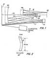
- Fig. 1is a schematic illustration of the projection optical system of the present invention.
- Fig. 2is a plan view of the ring portion or arcuate image field provided by the present invention.
- Fig. 3is a schematic drawing illustrating the use of the present invention in a scanning microlithographic apparatus.
- FIG. 1schematically illustrates one embodiment of the present invention.
- An illumination source 13which may be any illumination source that can provide electromagnetic radiation in the desired wavelength in the extreme ultraviolet, for example in the range from 11 to 12 nm.
- the illumination source 13may provide a desired illumination profile and intensity. For example, an intensity distribution that is not uniform along one dimension, such as a radial width, and is uniform along another dimension, such as in a tangent field direction or along the length of an arc, may be utilized thereby providing Kohler illumination or a uniform intensity distribution.
- the electromagnetic radiation from illumination source 13is received by reticle 10.
- Reticle 10is preferably a reticle having a predetermined line pattern thereon which is used for the manufacture of semiconductor devices.
- Reticle 10may be of the reflective type as illustrated, or a transmissive type.
- the reticle 10is placed at the long conjugate end of the reduction optical system.
- the electromagnetic radiation reflected from reticle 10is collected by a first convex mirror M1.
- the rays 11 of electromagnetic radiation from the reticle 10diverge.
- the first convex mirror M1has a negative power and causes the rays 12 of electromagnetic radiation reflected from the convex mirror M1 to also diverge.
- the rays 12 of electromagnetic radiation reflected from the convex mirror M1are collected by a concave mirror M2.
- the concave mirror M2has a positive power causing the rays 14 of electromagnetic radiation reflected therefrom to converge.
- the rays 14 of electromagnetic radiation reflected from concave mirror M2are collected by convex mirror M3.
- An aperture stop 22is formed at or near the surface of convex mirror M3.
- Convex mirror M3has a negative power causing the rays 16 of electromagnetic radiation reflected therefrom to diverge.
- the rays 16 of electromagnetic radiation reflected from convex mirror M3are collected by concave mirror M4.
- the rays 18 of electromagnetic radiation reflected from concave mirror M4are imaged onto a wafer 20 at an image plane. Wafer 20 is placed at the short conjugate end of the reduction optical system.
- the mirrors M1, M2, M3, and M4preferably have a common optical axis OA.
- the rays 11, 12, 14, 16, and 18form the optical path of the electromagnetic radiation in the optical system.
- the mirrors M1, M2, M3, and M4are preferably spaced relatively far apart. This has the benefit of minimizing the angular variations of light beams or rays 11, 12, 14, 16, and 18 hitting the mirrors M1, M2, M3, and M4. This improves system performance in that known reflective coatings typically used for extreme ultra violet wavelengths (EUV) are angle-sensitive. Additionally, this allows for a larger ring field radius for a given reticle 10 to wafer 20 distance. The following distances are therefore preferable.
- the distance between the reticle 10 and the reflective surface of mirror M1being greater than eighty percent of the distance between the reticle 10 and wafer 20.
- the distance between the reflective surfaces of mirrors M1 and M2being greater than seventy percent of the distance between the reticle 10 and wafer 20.
- the distance between the reflective surfaces of mirrors M2 and M3being greater than fifty percent of the distance between the reticle 10 and wafer 20.
- the distance between the reflective surfaces of mirrors M3 and M4being greater than twenty-five percent of the distance between the reticle 10 and wafer 20.
- the distance between the reflective surface of mirror M4 and the waferbeing greater than fifty percent of the distance between the reticle 10 and wafer 20.
- the optical systemillustrated in Fig. 1, may be made according to the construction data of the following Tables 1 and 1A.
- the construction datacontains some un-numbered surfaces referred to as dummies by those skilled in the art and are typically needed for the design to control the passage of light beams next to the mirrors.
- the un-numbered surfacescould be removed, however the thickness or distance before and after them would be added so that the thickness or distance between the mirrors remains the same.
- the optical projection system of the present inventionconstructed according to the construction data of Tables 1 and 1A, has a maximum numerical aperture equal to 0.1 and a four-to-one reduction ratio.
- a step and scan photolithography system using this projection systemwill be able to print features as small as 0.05 microns over an instantaneous annular image field of up to 50mm x 2 mm at the wafer.
- This image fieldcan be scanned to cover a field on the wafer of at least 50mm x 50 mm, thereby allowing a dramatic increase in circuit pattern density and complexity over current deep UV, 193 to 248 nm photolithography systems.
- the relatively large image fieldgreatly increases throughput and thereby increases the efficiency of systems utilizing the present invention.
- the projection optics of the present inventionare also relatively compact, having a reticle to wafer distance of less than 900 mm.
- Fig. 2illustrates the image field created by the present invention.
- the image field 24is an arcuate slit having a lateral dimension of approximately 2 mm and a longitudinal dimension of about 50 mm.
- the image field 24is generally scanned in the direction of arrow 26.
- the arcuate or annular slitis formed from portions of concentric circles having a radii of 49 and 51 mm, respectively.
- the residual design aberrationsare smaller than the Marechal criterion for diffraction limited imagery, 0.07 waves r.m.s. at an 11 nm wavelength.
- This systemwill likely be illuminated over the central 1.5 mm of the aberration corrected annulus, with an intensity distribution peaked near a central 50mm field radius and following that of the point source in the radial field direction, so called critical illumination. Kohler illumination, uniform intensity distribution, is assumed in the tangential field direction.
- the systemis telecentric at the wafer, but not at the reticle. This allows for oblique illumination of a spectrally reflected reticle, as is well known in the art.
- the present inventionby utilizing the unique mirror sequence of convex, concave, convex, and concave, in combination with an aperture stop coincident with the third mirror, makes possible very efficient projection optics having a relatively large annular image field. This results in improved throughput and therefore manufacturing efficiencies. Accordingly, the present invention advances the art of microlithography or photolithography and in particular, reduction projection optics used for a scanning lithographic system.
- Fig. 3is a block diagram illustrating generally a microlithography system utilizing projection optics according to the present invention.
- An illumination system 30illuminates a transmissive reticle 32.
- Projection optics 34according to the present invention, project the image of the reticle 32 onto a photosensitive resist covered substrate or wafer 36. Only a portion of the image of the reticle 32 is projected onto the wafer 36 at any one time. The image field of the projection optics 34 being smaller then the reticle 32 or wafer 36, the entire wafer 36 is exposed by scanning the retcile and wafer.
- Both the reticle stage 38 and wafer stage 40move in synchronization. However, because the optical system provides reduction, the reticle stage 38 moves at a different rate than the wafer stage 40. The difference in rate is proportional to the reduction.
- Control 42controls the movement of the reticle stage 38 and wafer stage 40.
Landscapes
- Physics & Mathematics (AREA)
- General Physics & Mathematics (AREA)
- Optics & Photonics (AREA)
- Health & Medical Sciences (AREA)
- Toxicology (AREA)
- Exposure And Positioning Against Photoresist Photosensitive Materials (AREA)
- Lenses (AREA)
- Exposure Of Semiconductors, Excluding Electron Or Ion Beam Exposure (AREA)
Description
- The present invention relates in general to semiconductormanufacturing using photolithography or microlithography, andmore particularly to an optical projection system for use in theextreme ultraviolet wavelength region, for example from 11 to 13nm.
- Semiconductor devices are typically manufactured byprojecting an image of a reticle containing a circuit patternonto a photosensitive resist covered wafer. As the feature sizeof the circuit elements become smaller, there is a need for theuse of smaller or shorter wavelengths of light or electromagneticradiation use in exposing the photosensitive resist coveredwafer. However, many difficulties arise in developing opticaldesigns for projecting the image of a reticle onto aphotosensitive substrate at the required short wavelengths of electromagnetic radiation in the extreme ultraviolet and soft X-rayregion. One such optical projection system is disclosed inU.S. Patent 5,353,322 entitled "Lens Systems For X-Ray ProjectionLithography Camera" issuing to Bruning et al on October 4, 1994.Therein disclosed is a three mirror projection system used inlithography at X-ray wavelengths to image a mask on a wafer. Alsodisclosed is a methodology for providing optimum solutions withinregions of two dimensional magnification space defined by themagnification of a convex mirror as one coordinate and the ratioof the magnification of a pair of concave mirrors optically onopposite sides of the convex mirror as another coordinate. Anoptical system is discloses having, from the image to the objectend, a concave mirror, a convex mirror, and a concave mirror.Bruning et al specifically advocates the use of a three-mirrorsystem as opposed to other two and four mirror systems. Whilethis optical system permits small residual aberrations over arelatively large field, there is a lack of an accessible aperturestop. Additionally, there is the disadvantage that there will besubtle variations in effective numerical aperture, and thereforeimage size around the annular field. Another projection opticalsystem is disclosed in U.S. Patent 5,315,629 entitled "Ring FieldLithography" and issuing to Jewell et al on May 24, 1994. Therein disclosed is a ring field projection apparatus for usewith X-ray radiation that has a relatively large slit width of atleast 0.5 mm. A folding mirror is also disclosed so that theprojection optics can be placed between the mask and wafer.Therein disclosed is a mirror configuration or sequence from thereticle or object to the wafer or image of a concave mirror, aconvex mirror, a concave mirror, and a convex mirror. Jewell etal specifically teaches away from the use of a negative or convexfirst mirror indicating that it was found that the telecentricrequirement in unobscured configuration could not be met. Whilethe prior art projection optical systems have proven adequate formany applications, they are not without design compromises thatmay not provide an optimum solution in all applications.Therefore, there is a need for a projection optical system thatcan be used in the extreme ultraviolet(EUV) or soft X-raywavelength region that has a relatively large image field withacceptable imaging for improving throughput. It is also desirablethat the image field have an acceptable aspect ratio. Thisreduces the difficulty of providing illumination uniformity ascompared to narrow slits with a high aspect ratio.
- Tanya E. Jewell describes in "The Journal of Vacuum Science andTechnology" B, 8 (1990) Nov/Dec, No. 6, pp. 1519-1523, a four mirroranastigmat as a reflective system for soft x-ray projection lithography in areflective systems design study.
- US Patent No. 5,410,434 describes a reflective projection system with arelatively wide field of view that comprises two concave and two convex sphericalmirrors situated in certain non-light blocking positions with respect to oneanother for deriving, with negligible image aberrations, a projected magnified ordemagnified image.
- The present invention relates to an all reflecting ringfield projection optical system designed for use with wavelengthsin the extreme ultraviolet, including wavelengths in the 11 to 13nm range, or soft X-rays. The present invention comprises aplurality of curved mirrors providing a reduction from a longconjugate end to a short conjugate end. The mirror order orsequence from the long conjugate end to the short conjugate endis a first negative power convex mirror, a first positive powerconcave mirror, a second negative convex mirror, and a secondpositive concave mirror. The plurality of curved mirrors arearranged such that an aperture stop is coincident at or near thethird mirror or second negative convex mirror. The reflectivesurfaces of each mirror are spaced or separated by a distancegreater than twenty-five percent of the total distance betweenthe long conjugate end and the short conjugate end.
- Accordingly, it is an object of the present invention toprovide a projection optical system that has a relatively largeimage field size.
- It is another object of the present invention to provide anaccessible aperture stop.
- It is an advantage of the present invention that a variableiris may be utilized at the aperture stop.
- It is another advantage of the present invention that theobject and image positions are located or positioned tofacilitate scanning.
- It is an advantage of the present invention that it canprint feature sizes as small as 0.05 microns and has a slot widthof 2 mm.
- It is a feature of the present invention that the firstmirror from the long conjugate end to the short conjugate end isa negative power convex mirror.
- It is another feature of the present invention that themirrors are spaced relatively far apart to minimize the angularvariations of light beams hitting the mirrors.
- These and other objects, advantages, and features willbecome readily apparent in view of the following detaileddescription.
- Fig. 1 is a schematic illustration of the projection opticalsystem of the present invention.
- Fig. 2 is a plan view of the ring portion or arcuate imagefield provided by the present invention.
- Fig. 3 is a schematic drawing illustrating the use of thepresent invention in a scanning microlithographic apparatus.
- Fig. 1 schematically illustrates one embodiment of thepresent invention. An
illumination source 13, which may be anyillumination source that can provide electromagnetic radiation inthe desired wavelength in the extreme ultraviolet, for example inthe range from 11 to 12 nm. Theillumination source 13 mayprovide a desired illumination profile and intensity. Forexample, an intensity distribution that is not uniform along onedimension, such as a radial width, and is uniform along anotherdimension, such as in a tangent field direction or along thelength of an arc, may be utilized thereby providing Kohlerillumination or a uniform intensity distribution. Theelectromagnetic radiation fromillumination source 13 is receivedby reticle 10. Reticle 10 is preferably a reticle having apredetermined line pattern thereon which is used for themanufacture of semiconductor devices. Reticle 10 may be of the reflective type as illustrated, or a transmissive type. Thereticle 10 is placed at the long conjugate end of the reductionoptical system. The electromagnetic radiation reflected fromreticle 10 is collected by a first convex mirror M1. The rays 11of electromagnetic radiation from the reticle 10 diverge. Thefirst convex mirror M1 has a negative power and causes therays 12 of electromagnetic radiation reflected from the convex mirrorM1 to also diverge. Therays 12 of electromagnetic radiationreflected from the convex mirror M1 are collected by a concavemirror M2. The concave mirror M2 has a positive power causing therays 14 of electromagnetic radiation reflected therefrom toconverge. The rays 14 of electromagnetic radiation reflected fromconcave mirror M2 are collected by convex mirror M3. Anaperturestop 22 is formed at or near the surface of convex mirror M3.Convex mirror M3 has a negative power causing therays 16 ofelectromagnetic radiation reflected therefrom to diverge. Therays 16 of electromagnetic radiation reflected from convex mirrorM3 are collected by concave mirror M4. Therays 18 ofelectromagnetic radiation reflected from concave mirror M4 areimaged onto awafer 20 at an image plane.Wafer 20 is placed atthe short conjugate end of the reduction optical system. Themirrors M1, M2, M3, and M4 preferably have a common optical axis OA. Therays wafer 20distance. The following distances are therefore preferable. Thedistance between the reticle 10 and the reflective surface ofmirror M1 being greater than eighty percent of the distancebetween the reticle 10 andwafer 20. The distance between thereflective surfaces of mirrors M1 and M2 being greater thanseventy percent of the distance between the reticle 10 andwafer 20. The distance between the reflective surfaces of mirrors M2and M3 being greater than fifty percent of the distance betweenthe reticle 10 andwafer 20. The distance between the reflectivesurfaces of mirrors M3 and M4 being greater than twenty-fivepercent of the distance between the reticle 10 andwafer 20. Thedistance between the reflective surface of mirror M4 and the wafer being greater than fifty percent of the distance betweenthe reticle 10 andwafer 20. - In a preferred configuration the optical system,illustrated in Fig. 1, may be made according to the constructiondata of the following Tables 1 and 1A. The construction datacontains some un-numbered surfaces referred to as dummies bythose skilled in the art and are typically needed for the designto control the passage of light beams next to the mirrors. Theun-numbered surfaces could be removed, however the thickness ordistance before and after them would be added so that thethickness or distance between the mirrors remains the same.
ElementNumber Radius ofCurvature Thickness ApertureDiameter Glass Object Infinite 125.0000 384.9520 682.5197 1 A(1) -682.5197 282.3516 Reflective 2 A(2) 556.6306 318.7516 Reflective Aperture Stop 50.0710 3 A(3) -556.6306 50.0710 Reflective 365.8025 299.9381 4 A(4) -299.9381 194.4209 Reflective 255.2926 556.6306 142.7533 Image Distance = 209.2224 Image Infinite 102.0002 - The aspheric constants are provided according to the following equation and Table 1A
Aspheric Curv K A B C D A(1) 0.00038658 0.000000 -1.94905E-10 -9.77521E-17 7.55027E-21 -3.03099E-25 A(2) 0.00084708 0.000000 -6.71274E-11 -8.42747E-17 -8.35108E-22 9.74444E-28 A(3) 0.00243452 0.000000 5.25375E-10 -3.50002E-15 1.26244E-17 -7.16624E-21 A(4) 0.00196174 0.000000 1.28463E-10 7.98681E-16 -1.24539E-20 5.30348E-25 - The optical projection system of the present invention,constructed according to the construction data of Tables 1 and1A, has a maximum numerical aperture equal to 0.1 and a four-to-onereduction ratio. A step and scan photolithography systemusing this projection system will be able to print features assmall as 0.05 microns over an instantaneous annular image fieldof up to 50mm x 2 mm at the wafer. This image field can bescanned to cover a field on the wafer of at least 50mm x 50 mm,thereby allowing a dramatic increase in circuit pattern densityand complexity over current deep UV, 193 to 248 nmphotolithography systems. The relatively large image fieldgreatly increases throughput and thereby increases the efficiencyof systems utilizing the present invention. The projection opticsof the present invention are also relatively compact, having areticle to wafer distance of less than 900 mm.
- Fig. 2 illustrates the image field created by the presentinvention. The
image field 24 is an arcuate slit having a lateraldimension of approximately 2 mm and a longitudinal dimension ofabout 50 mm. Theimage field 24 is generally scanned in thedirection ofarrow 26. The arcuate or annular slit is formed fromportions of concentric circles having a radii of 49 and 51 mm,respectively. At the wafer, the residual design aberrations are smaller than the Marechal criterion for diffraction limitedimagery, 0.07 waves r.m.s. at an 11 nm wavelength. This systemwill likely be illuminated over the central 1.5 mm of theaberration corrected annulus, with an intensity distributionpeaked near a central 50mm field radius and following that of thepoint source in the radial field direction, so called criticalillumination. Kohler illumination, uniform intensitydistribution, is assumed in the tangential field direction. Thesystem is telecentric at the wafer, but not at the reticle. Thisallows for oblique illumination of a spectrally reflectedreticle, as is well known in the art. - The present invention, by utilizing the unique mirrorsequence of convex, concave, convex, and concave, in combinationwith an aperture stop coincident with the third mirror, makespossible very efficient projection optics having a relativelylarge annular image field. This results in improved throughputand therefore manufacturing efficiencies. Accordingly, thepresent invention advances the art of microlithography orphotolithography and in particular, reduction projection opticsused for a scanning lithographic system.
- Fig. 3 is a block diagram illustrating generally amicrolithography system utilizing projection optics according to the present invention. An
illumination system 30 illuminates atransmissive reticle 32.Projection optics 34, according to thepresent invention, project the image of thereticle 32 onto aphotosensitive resist covered substrate orwafer 36. Only aportion of the image of thereticle 32 is projected onto thewafer 36 at any one time. The image field of theprojectionoptics 34 being smaller then thereticle 32 orwafer 36, theentire wafer 36 is exposed by scanning the retcile and wafer.Both thereticle stage 38 andwafer stage 40 move insynchronization. However, because the optical system providesreduction, thereticle stage 38 moves at a different rate thanthewafer stage 40. The difference in rate is proportional to thereduction.Control 42 controls the movement of thereticle stage 38 andwafer stage 40. - Although the preferred embodiment has been illustrated anddescribed, it will be obvious to those skilled in the art thatvarious modifications may be made without departing from thescope of this invention as set out in the claims.
Claims (17)
- A ring field reduction projection optical system having a pluralityof curved mirrors alternating from convex to concave arrangedsuch that electromagnetic radiation is reflected along an opticalpath from a first convex mirror to a first concave mirror to asecond convex mirror to a second concave mirror, an optical axis,whereby the centers of curvature of all four mirrors lie on theoptical axis, an aperture stop formed near said second convexmirror, and a length from a long conjugate end to a shortconjugate end, whereby an arcuate image field is formed at theshort conjugate end,
characterized in that
said first convex mirror is positioned from the long conjugate endin a direction of the optical path a first distance greater thaneighty percent of the length;
said first concave mirror is positioned from said first convexmirror in a direction of the optical path a second distance greaterthan seventy percent of the length;
said second convex mirror is positioned from said first concavemirror in a direction of the optical path a third distance greaterthan fifty percent of the length; and
said second concave mirror is positioned from said secondconvex mirror in a direction of the optical path a fourth distancegreater than twenty-five percent of the length. - A ring field reduction projection optical system as in claim 1having a long conjugate end and a short conjugate end for use inthe extreme ultraviolet wavelength region comprising:a plurality of curved mirrors alternating from convex to concavefrom the long conjugate end to the short conjugate end, wherebyan arcuate image field is formed.
- A ring field reduction projection optical system as in claim 2wherein:the arcuate image field has at least 0.1 micron resolution and a radialwidth of 2 mm and a longitudinal length of substantially 50 mm.
- A ring field reduction projection optical system as in claim 2wherein:said plurality of curved mirrors are aspheric.
- A ring field reduction projection optical system as in claim 4wherein:said plurality of curved mirrors provides a reduction ratio of fourto one.
- A ring field reduction projection optical system as in claim 1having an optical axis and an optical path, from a long conjugateend to a short conjugate end comprising:arranged such that electromagnetic radiation is reflected alongthe optical path from said first convex mirror to said first concavemirror to said second convex mirror to said second concavemirror, whereby an arcuate image field is formed.a first convex mirror;a first concave mirror;a second convex mirror; anda second concave mirror,
- A ring field reduction projection optical system as in claim 6wherein:said first concave mirror is positioned along the optical axisbetween the long conjugate end and said second concave mirror.
- A ring field reduction projection optical system as in claim 6wherein:said second convex mirror is positioned along the optical axisbetween said second concave mirror and said first convex mirrorand the distance between said second concave mirror and saidsecond convex mirror perpendicular to the optical axis is smallerthan the distance between first convex mirror and said secondconvex mirror.
- A ring field reduction projection optical system as in claim 6wherein:said first convex mirror forms rays of electromagnetic radiationthat diverge along the optical path between the long conjugateend and the short conjugate end.
- A ring field reduction projection optical system as in claim 9wherein:said first concave mirror forms rays of electromagnetic radiationthat converge along the optical path between the long conjugateend and the short conjugate end.
- A ring field reduction projection optical system as in claim 1 alongan optical path, from a long conjugate end to a short conjugateend comprising:arranged such that electromagnetic radiation is reflected fromsaid first convex mirror to said first concave mirror to said secondconvex mirror to said second concave mirror and the positioningalong an optical axis(OA) is such that said first convex mirror(M1)is positioned between the short conjugate end and said secondconvex mirror(M3), said first concave mirror(M2) is positionedbetween the long conjugate end and said second concavemirror(M4), said second convex mirror(M3) is positioned betweensaid first convex mirror(M1) and said second concave mirror(M4),and said second concave mirror(M4) is positioned between saidfirst concave mirror(M2) and said second convex mirror(M3),a first convex mirror(M1);a first concave mirror(M2);a second convex mirror(M3); anda second concave mirror(M4),
whereby an arcuate image field is formed. - A ring field reduction projection optical system as in claim 11wherein:said first convex mirror(M1), said first concave mirror(M2), saidsecond convex mirror(M3), and said second concave mirror(M4)have aspheric reflective surfaces.
- A ring field reduction projection optical system as in claim 11wherein:the arcuate image field has at least 0.1 micron resolution and aradial width of 2 mm and a longitudinal length of substantially 50mm.
- A ring field reduction projection optical system as in claim 1 usedin the manufacture of semiconductor devices, from the longconjugate end to the short conjugate end comprising:a first negative power convex mirror positioned to receiveelectromagnetic radiation, the electromagnetic radiation reflectedfrom said first negative power convex mirror forming divergingrays;a first positive power concave mirror positioned to receiveelectromagnetic radiation reflected from said first negative powerconvex mirror, the electromagnetic radiation reflected from saidfirst positive power concave mirror forming converging rays;a second negative power convex mirror positioned to receiveelectromagnetic radiation reflected from said first positive powerconcave mirror, the electromagnetic radiation reflected from saidsecond negative power convex mirror forming diverging rays; anda second positive power concave mirror positioned to receive electromagnetic radiation reflected from said second negativepower convex mirror, the electromagnetic radiation reflected fromsaid second positive power concave mirror forming an arcuateimage field having at least 0.1 micron resolution and a radialwidth of 2 mm and a longitudinal length of substantially 50 mm.
- A ring field reduction projection optical system as in claim 1having an optical axis, an optical path, and a length from a longconjugate end to a short conjugate end comprising:arranged such that electromagnetic radiation is reflected alongthe optical path from said first convex mirror to said first concavemirror to said second convex mirror to said second concavemirror, and the distance between each of the reflective surfacesof said mirrors in a direction of the optical path along the opticalaxis is grater than twenty-five percent of the length from the longconjugate end to the short conjugate end, whereby an arcuateimage field is formed.a first convex mirror;a first concave mirror;a second convex mirror; anda second concave mirror,
- A ring field reduction projection optical system as in claim 1wherein:said second concave mirror is positioned from the short conjugateend a fifth distance greater than fifty percent of the length.
- A ring field reduction projection optical system as in claim 1, fromthe long conjugate end to the short conjugate end comprising:arranged such that electromagnetic radiation is reflected fromsaid first convex mirror to said first concave mirror to said secondconvex mirror to said second concave mirror, and constructedaccording the to following construction data,a first convex mirror;a first concave mirror;a second convex mirror; anda second concave mirror,
Element
NumberRadius ofCurvature Thickness(mm) ApertureDiameter (mm) Glass Object Infinite 125.0000 384.9520 682.5197 1 A(1) -682.5197 282.3516 Reflective 2 A(2) 556.6306 318.7516 Reflective Aperture Stop 50.0710 3 A(3) -556.6306 50.0710 Reflective 365.8025 299.9381 4 A(4) -299.9381 194.4209 Reflective 255.2926 556.6306 142.7533 Image Distance
=209.2224 Image Infinite 102.0002 Aspheric Curve K A B C D A(1) 0.00038658 0.000000 -1.94905E-10 -9.77521E-17 7.55027E-21 -3.03099E-25 A(2) 0.00084708 0.000000 -6.71274E-11 -8.42747E-17 -8.35108E-22 9.74444E-28 A(3) 0.00243452 0.000000 5.25375E-10 -3.50002E-15 1.26244E-17 -7.16624E-21 A(4) 0.00196174 0.000000 1.28463E-10 7.98681E-16 -1.24539E-20 5.30348E-25
Applications Claiming Priority (2)
| Application Number | Priority Date | Filing Date | Title |
|---|---|---|---|
| US08/933,272US5956192A (en) | 1997-09-18 | 1997-09-18 | Four mirror EUV projection optics |
| US933272 | 1997-09-18 |
Publications (3)
| Publication Number | Publication Date |
|---|---|
| EP0903605A2 EP0903605A2 (en) | 1999-03-24 |
| EP0903605A3 EP0903605A3 (en) | 2000-05-17 |
| EP0903605B1true EP0903605B1 (en) | 2003-04-09 |
Family
ID=25463660
Family Applications (1)
| Application Number | Title | Priority Date | Filing Date |
|---|---|---|---|
| EP98117168AExpired - LifetimeEP0903605B1 (en) | 1997-09-18 | 1998-09-10 | Four mirror EUV projection optics |
Country Status (6)
| Country | Link |
|---|---|
| US (1) | US5956192A (en) |
| EP (1) | EP0903605B1 (en) |
| JP (1) | JP4309980B2 (en) |
| KR (1) | KR100597471B1 (en) |
| CA (1) | CA2247709A1 (en) |
| DE (1) | DE69813126T2 (en) |
Families Citing this family (40)
| Publication number | Priority date | Publication date | Assignee | Title |
|---|---|---|---|---|
| US6081578A (en)* | 1997-11-07 | 2000-06-27 | U.S. Philips Corporation | Three-mirror system for lithographic projection, and projection apparatus comprising such a mirror system |
| DE10053587A1 (en) | 2000-10-27 | 2002-05-02 | Zeiss Carl | Lighting system with variable adjustment of the illumination |
| DE19923609A1 (en)* | 1998-05-30 | 1999-12-02 | Zeiss Carl Fa | Reduction objective useful in projector for deep ultraviolet microlithography in chip manufacture |
| US6577443B2 (en) | 1998-05-30 | 2003-06-10 | Carl-Zeiss Stiftung | Reduction objective for extreme ultraviolet lithography |
| US7151592B2 (en)* | 1999-02-15 | 2006-12-19 | Carl Zeiss Smt Ag | Projection system for EUV lithography |
| US6985210B2 (en)* | 1999-02-15 | 2006-01-10 | Carl Zeiss Smt Ag | Projection system for EUV lithography |
| USRE42118E1 (en)* | 1999-02-15 | 2011-02-08 | Carl-Zeiss-Smt Ag | Projection system for EUV lithography |
| US6188513B1 (en) | 1999-03-15 | 2001-02-13 | Russell Hudyma | High numerical aperture ring field projection system for extreme ultraviolet lithography |
| US6033079A (en) | 1999-03-15 | 2000-03-07 | Hudyma; Russell | High numerical aperture ring field projection system for extreme ultraviolet lithography |
| JP4717974B2 (en)* | 1999-07-13 | 2011-07-06 | 株式会社ニコン | Catadioptric optical system and projection exposure apparatus provided with the optical system |
| WO2001007967A1 (en) | 1999-07-22 | 2001-02-01 | Corning Incorporated | Extreme ultraviolet soft x-ray projection lithographic method and mask devices |
| EP1093021A3 (en) | 1999-10-15 | 2004-06-30 | Nikon Corporation | Projection optical system as well as equipment and methods making use of said system |
| TW538256B (en) | 2000-01-14 | 2003-06-21 | Zeiss Stiftung | Microlithographic reduction projection catadioptric objective |
| US6776006B2 (en) | 2000-10-13 | 2004-08-17 | Corning Incorporated | Method to avoid striae in EUV lithography mirrors |
| TW573234B (en) | 2000-11-07 | 2004-01-21 | Asml Netherlands Bv | Lithographic projection apparatus and integrated circuit device manufacturing method |
| US6558261B1 (en) | 2000-11-15 | 2003-05-06 | Honeywell International Inc. | Actuator drive and display mechanism |
| JP2004514943A (en)* | 2000-11-28 | 2004-05-20 | カール・ツアイス・エスエムテイ・アーゲー | Catadioptric projection system for 157nm lithography |
| US6832493B2 (en) | 2002-02-27 | 2004-12-21 | Corning Incorporated | High purity glass bodies formed by zero shrinkage casting |
| US6829908B2 (en) | 2002-02-27 | 2004-12-14 | Corning Incorporated | Fabrication of inclusion free homogeneous glasses |
| US20030235682A1 (en)* | 2002-06-21 | 2003-12-25 | Sogard Michael R. | Method and device for controlling thermal distortion in elements of a lithography system |
| US6975385B2 (en)* | 2002-11-08 | 2005-12-13 | Canon Kabushiki Kaisha | Projection optical system and exposure apparatus |
| US6853440B1 (en) | 2003-04-04 | 2005-02-08 | Asml Netherlands B.V. | Position correction in Y of mask object shift due to Z offset and non-perpendicular illumination |
| US8208198B2 (en) | 2004-01-14 | 2012-06-26 | Carl Zeiss Smt Gmbh | Catadioptric projection objective |
| US7466489B2 (en) | 2003-12-15 | 2008-12-16 | Susanne Beder | Projection objective having a high aperture and a planar end surface |
| WO2005059645A2 (en)* | 2003-12-19 | 2005-06-30 | Carl Zeiss Smt Ag | Microlithography projection objective with crystal elements |
| US7463422B2 (en)* | 2004-01-14 | 2008-12-09 | Carl Zeiss Smt Ag | Projection exposure apparatus |
| KR101204114B1 (en)* | 2004-01-14 | 2012-11-23 | 칼 짜이스 에스엠티 게엠베하 | Catadioptric projection objective |
| US20080151365A1 (en) | 2004-01-14 | 2008-06-26 | Carl Zeiss Smt Ag | Catadioptric projection objective |
| US7712905B2 (en) | 2004-04-08 | 2010-05-11 | Carl Zeiss Smt Ag | Imaging system with mirror group |
| CN100483174C (en) | 2004-05-17 | 2009-04-29 | 卡尔蔡司Smt股份公司 | Catadioptric projection objective with intermediate images |
| JP4337648B2 (en)* | 2004-06-24 | 2009-09-30 | 株式会社ニコン | EUV LIGHT SOURCE, EUV EXPOSURE APPARATUS, AND METHOD FOR MANUFACTURING SEMICONDUCTOR DEVICE |
| JP2008533709A (en)* | 2005-03-08 | 2008-08-21 | カール ツァイス エスエムテー アーゲー | Microlithography projection optical system with handleable aperture or aperture stop |
| JP4918542B2 (en)* | 2005-05-13 | 2012-04-18 | カール・ツァイス・エスエムティー・ゲーエムベーハー | EUV projection optical system with six reflectors |
| JP5045429B2 (en)* | 2007-12-27 | 2012-10-10 | コニカミノルタアドバンストレイヤー株式会社 | Oblique projection optical system |
| JP5294804B2 (en)* | 2008-10-31 | 2013-09-18 | 三菱電機株式会社 | Optical adjustment device |
| DE102009008644A1 (en)* | 2009-02-12 | 2010-11-18 | Carl Zeiss Smt Ag | Imaging optics and projection exposure system for microlithography with such an imaging optics |
| JP4935886B2 (en)* | 2009-12-10 | 2012-05-23 | 三菱電機株式会社 | Image reading device |
| WO2013118615A1 (en) | 2012-02-06 | 2013-08-15 | 株式会社ニコン | Reflective image-forming optical system, exposure apparatus, and device manufacturing method |
| CN105589305B (en)* | 2015-12-21 | 2017-10-03 | 中国科学院长春光学精密机械与物理研究所 | Visual field independent positioning method in micro optical projection system wave aberration detection process |
| JP2018157503A (en)* | 2017-03-21 | 2018-10-04 | 富士ゼロックス株式会社 | Reading device |
Family Cites Families (11)
| Publication number | Priority date | Publication date | Assignee | Title |
|---|---|---|---|---|
| US3748015A (en)* | 1971-06-21 | 1973-07-24 | Perkin Elmer Corp | Unit power imaging catoptric anastigmat |
| US4240707A (en)* | 1978-12-07 | 1980-12-23 | Itek Corporation | All-reflective three element objective |
| US4650315A (en)* | 1985-05-10 | 1987-03-17 | The Perkin-Elmer Corporation | Optical lithographic system |
| US4733955A (en)* | 1986-04-14 | 1988-03-29 | Hughes Aircraft Company | Reflective optical triplet having a real entrance pupil |
| EP0252734B1 (en)* | 1986-07-11 | 2000-05-03 | Canon Kabushiki Kaisha | X-ray reduction projection exposure system of reflection type |
| US4747678A (en)* | 1986-12-17 | 1988-05-31 | The Perkin-Elmer Corporation | Optical relay system with magnification |
| US5063586A (en)* | 1989-10-13 | 1991-11-05 | At&T Bell Laboratories | Apparatus for semiconductor lithography |
| US5315629A (en)* | 1990-10-10 | 1994-05-24 | At&T Bell Laboratories | Ringfield lithography |
| US5353322A (en)* | 1992-05-05 | 1994-10-04 | Tropel Corporation | Lens system for X-ray projection lithography camera |
| US5410434A (en)* | 1993-09-09 | 1995-04-25 | Ultratech Stepper, Inc. | Reflective projection system comprising four spherical mirrors |
| US5815310A (en)* | 1995-12-12 | 1998-09-29 | Svg Lithography Systems, Inc. | High numerical aperture ring field optical reduction system |
- 1997
- 1997-09-18USUS08/933,272patent/US5956192A/ennot_activeExpired - Fee Related
- 1998
- 1998-09-10EPEP98117168Apatent/EP0903605B1/ennot_activeExpired - Lifetime
- 1998-09-10DEDE69813126Tpatent/DE69813126T2/ennot_activeExpired - Fee Related
- 1998-09-16KRKR1019980038158Apatent/KR100597471B1/ennot_activeExpired - Fee Related
- 1998-09-18CACA002247709Apatent/CA2247709A1/ennot_activeAbandoned
- 1998-09-18JPJP26493798Apatent/JP4309980B2/ennot_activeExpired - Fee Related
Also Published As
| Publication number | Publication date |
|---|---|
| DE69813126D1 (en) | 2003-05-15 |
| DE69813126T2 (en) | 2004-03-04 |
| JPH11249313A (en) | 1999-09-17 |
| EP0903605A3 (en) | 2000-05-17 |
| KR100597471B1 (en) | 2006-10-24 |
| JP4309980B2 (en) | 2009-08-05 |
| EP0903605A2 (en) | 1999-03-24 |
| CA2247709A1 (en) | 1999-03-18 |
| US5956192A (en) | 1999-09-21 |
| KR19990029826A (en) | 1999-04-26 |
Similar Documents
| Publication | Publication Date | Title |
|---|---|---|
| EP0903605B1 (en) | Four mirror EUV projection optics | |
| KR100991049B1 (en) | Projection exposure apparatus | |
| KR101149267B1 (en) | Microlithography projection optical system, method for manufacturing a device and method to design an optical surface | |
| US8632195B2 (en) | Catoptric objectives and systems using catoptric objectives | |
| USRE38421E1 (en) | Exposure apparatus having catadioptric projection optical system | |
| US7177076B2 (en) | 8-mirror microlithography projection objective | |
| US6244717B1 (en) | Reduction objective for extreme ultraviolet lithography | |
| EP1320854B1 (en) | Illumination system particularly for microlithography | |
| KR101309880B1 (en) | A six-mirror euv projection system with low incidence angles | |
| US9046787B2 (en) | Microlithographic projection exposure apparatus | |
| KR20020031057A (en) | 8-Mirror-microlithography -projection objective | |
| JP2005500566A (en) | Objective mirror with Hitomi obscuration | |
| US7626770B2 (en) | Illumination system with zoom objective | |
| US9612540B2 (en) | Method of operating a microlithographic apparatus | |
| US20040218164A1 (en) | Exposure apparatus | |
| KR100749015B1 (en) | Projection objectives and projection exposure devices for microlithography | |
| US20090009744A1 (en) | Illumination system for a microlithographic projection exposure apparatus | |
| KR100660504B1 (en) | Lithographic apparatus, illumination system, and optical element for rotating an intensity distribution | |
| US20200117099A1 (en) | Optical objective for operation in euv spectral region |
Legal Events
| Date | Code | Title | Description |
|---|---|---|---|
| PUAI | Public reference made under article 153(3) epc to a published international application that has entered the european phase | Free format text:ORIGINAL CODE: 0009012 | |
| AK | Designated contracting states | Kind code of ref document:A2 Designated state(s):DE FR GB IT NL | |
| AX | Request for extension of the european patent | Free format text:AL;LT;LV;MK;RO;SI | |
| PUAL | Search report despatched | Free format text:ORIGINAL CODE: 0009013 | |
| RIC1 | Information provided on ipc code assigned before grant | Free format text:7G 02B 13/14 A, 7G 02B 17/06 B, 7G 03F 7/20 B | |
| AK | Designated contracting states | Kind code of ref document:A3 Designated state(s):AT BE CH CY DE DK ES FI FR GB GR IE IT LI LU MC NL PT SE | |
| AX | Request for extension of the european patent | Free format text:AL;LT;LV;MK;RO;SI | |
| 17P | Request for examination filed | Effective date:20001117 | |
| AKX | Designation fees paid | Free format text:DE FR GB IT NL | |
| 17Q | First examination report despatched | Effective date:20010313 | |
| GRAG | Despatch of communication of intention to grant | Free format text:ORIGINAL CODE: EPIDOS AGRA | |
| GRAG | Despatch of communication of intention to grant | Free format text:ORIGINAL CODE: EPIDOS AGRA | |
| GRAH | Despatch of communication of intention to grant a patent | Free format text:ORIGINAL CODE: EPIDOS IGRA | |
| GRAH | Despatch of communication of intention to grant a patent | Free format text:ORIGINAL CODE: EPIDOS IGRA | |
| GRAA | (expected) grant | Free format text:ORIGINAL CODE: 0009210 | |
| AK | Designated contracting states | Designated state(s):DE FR GB IT NL | |
| REG | Reference to a national code | Ref country code:GB Ref legal event code:FG4D | |
| RAP2 | Party data changed (patent owner data changed or rights of a patent transferred) | Owner name:ASMLHOLDING, N.V. | |
| REG | Reference to a national code | Ref country code:GB Ref legal event code:732E | |
| NLT2 | Nl: modifications (of names), taken from the european patent patent bulletin | Owner name:ASML | |
| ET | Fr: translation filed | ||
| PLBE | No opposition filed within time limit | Free format text:ORIGINAL CODE: 0009261 | |
| STAA | Information on the status of an ep patent application or granted ep patent | Free format text:STATUS: NO OPPOSITION FILED WITHIN TIME LIMIT | |
| 26N | No opposition filed | Effective date:20040112 | |
| PGFP | Annual fee paid to national office [announced via postgrant information from national office to epo] | Ref country code:NL Payment date:20080915 Year of fee payment:11 Ref country code:IT Payment date:20080924 Year of fee payment:11 Ref country code:FR Payment date:20080912 Year of fee payment:11 | |
| PGFP | Annual fee paid to national office [announced via postgrant information from national office to epo] | Ref country code:GB Payment date:20080918 Year of fee payment:11 | |
| PGFP | Annual fee paid to national office [announced via postgrant information from national office to epo] | Ref country code:DE Payment date:20080919 Year of fee payment:11 | |
| REG | Reference to a national code | Ref country code:NL Ref legal event code:V1 Effective date:20100401 | |
| GBPC | Gb: european patent ceased through non-payment of renewal fee | Effective date:20090910 | |
| REG | Reference to a national code | Ref country code:FR Ref legal event code:ST Effective date:20100531 | |
| PG25 | Lapsed in a contracting state [announced via postgrant information from national office to epo] | Ref country code:NL Free format text:LAPSE BECAUSE OF NON-PAYMENT OF DUE FEES Effective date:20100401 Ref country code:FR Free format text:LAPSE BECAUSE OF NON-PAYMENT OF DUE FEES Effective date:20090930 Ref country code:DE Free format text:LAPSE BECAUSE OF NON-PAYMENT OF DUE FEES Effective date:20100401 | |
| PG25 | Lapsed in a contracting state [announced via postgrant information from national office to epo] | Ref country code:GB Free format text:LAPSE BECAUSE OF NON-PAYMENT OF DUE FEES Effective date:20090910 | |
| PG25 | Lapsed in a contracting state [announced via postgrant information from national office to epo] | Ref country code:IT Free format text:LAPSE BECAUSE OF NON-PAYMENT OF DUE FEES Effective date:20090910 |