EP0902538A2 - Article comprising a light-actuated micromechanical photonic switch - Google Patents
Article comprising a light-actuated micromechanical photonic switchDownload PDFInfo
- Publication number
- EP0902538A2 EP0902538A2EP98307019AEP98307019AEP0902538A2EP 0902538 A2EP0902538 A2EP 0902538A2EP 98307019 AEP98307019 AEP 98307019AEP 98307019 AEP98307019 AEP 98307019AEP 0902538 A2EP0902538 A2EP 0902538A2
- Authority
- EP
- European Patent Office
- Prior art keywords
- optical
- photogenerator
- article
- light
- mems
- Prior art date
- Legal status (The legal status is an assumption and is not a legal conclusion. Google has not performed a legal analysis and makes no representation as to the accuracy of the status listed.)
- Withdrawn
Links
Images


Classifications
- G—PHYSICS
- G02—OPTICS
- G02B—OPTICAL ELEMENTS, SYSTEMS OR APPARATUS
- G02B6/00—Light guides; Structural details of arrangements comprising light guides and other optical elements, e.g. couplings
- G02B6/24—Coupling light guides
- G02B6/26—Optical coupling means
- G02B6/35—Optical coupling means having switching means
- G02B6/3564—Mechanical details of the actuation mechanism associated with the moving element or mounting mechanism details
- G02B6/3568—Mechanical details of the actuation mechanism associated with the moving element or mounting mechanism details characterised by the actuating force
- G—PHYSICS
- G02—OPTICS
- G02B—OPTICAL ELEMENTS, SYSTEMS OR APPARATUS
- G02B6/00—Light guides; Structural details of arrangements comprising light guides and other optical elements, e.g. couplings
- G02B6/10—Light guides; Structural details of arrangements comprising light guides and other optical elements, e.g. couplings of the optical waveguide type
- G02B6/12—Light guides; Structural details of arrangements comprising light guides and other optical elements, e.g. couplings of the optical waveguide type of the integrated circuit kind
- G02B6/122—Basic optical elements, e.g. light-guiding paths
- G—PHYSICS
- G02—OPTICS
- G02B—OPTICAL ELEMENTS, SYSTEMS OR APPARATUS
- G02B6/00—Light guides; Structural details of arrangements comprising light guides and other optical elements, e.g. couplings
- G02B6/10—Light guides; Structural details of arrangements comprising light guides and other optical elements, e.g. couplings of the optical waveguide type
- G02B6/12—Light guides; Structural details of arrangements comprising light guides and other optical elements, e.g. couplings of the optical waveguide type of the integrated circuit kind
- G02B2006/12083—Constructional arrangements
- G02B2006/12104—Mirror; Reflectors or the like
- G—PHYSICS
- G02—OPTICS
- G02B—OPTICAL ELEMENTS, SYSTEMS OR APPARATUS
- G02B6/00—Light guides; Structural details of arrangements comprising light guides and other optical elements, e.g. couplings
- G02B6/24—Coupling light guides
- G02B6/26—Optical coupling means
- G02B6/35—Optical coupling means having switching means
- G02B6/351—Optical coupling means having switching means involving stationary waveguides with moving interposed optical elements
- G02B6/3512—Optical coupling means having switching means involving stationary waveguides with moving interposed optical elements the optical element being reflective, e.g. mirror
- G02B6/3514—Optical coupling means having switching means involving stationary waveguides with moving interposed optical elements the optical element being reflective, e.g. mirror the reflective optical element moving along a line so as to translate into and out of the beam path, i.e. across the beam path
- G—PHYSICS
- G02—OPTICS
- G02B—OPTICAL ELEMENTS, SYSTEMS OR APPARATUS
- G02B6/00—Light guides; Structural details of arrangements comprising light guides and other optical elements, e.g. couplings
- G02B6/24—Coupling light guides
- G02B6/26—Optical coupling means
- G02B6/35—Optical coupling means having switching means
- G02B6/351—Optical coupling means having switching means involving stationary waveguides with moving interposed optical elements
- G02B6/353—Optical coupling means having switching means involving stationary waveguides with moving interposed optical elements the optical element being a shutter, baffle, beam dump or opaque element
- G—PHYSICS
- G02—OPTICS
- G02B—OPTICAL ELEMENTS, SYSTEMS OR APPARATUS
- G02B6/00—Light guides; Structural details of arrangements comprising light guides and other optical elements, e.g. couplings
- G02B6/24—Coupling light guides
- G02B6/26—Optical coupling means
- G02B6/35—Optical coupling means having switching means
- G02B6/354—Switching arrangements, i.e. number of input/output ports and interconnection types
- G02B6/3544—2D constellations, i.e. with switching elements and switched beams located in a plane
- G02B6/3548—1xN switch, i.e. one input and a selectable single output of N possible outputs
- G02B6/3552—1x1 switch, e.g. on/off switch
- G—PHYSICS
- G02—OPTICS
- G02B—OPTICAL ELEMENTS, SYSTEMS OR APPARATUS
- G02B6/00—Light guides; Structural details of arrangements comprising light guides and other optical elements, e.g. couplings
- G02B6/24—Coupling light guides
- G02B6/26—Optical coupling means
- G02B6/35—Optical coupling means having switching means
- G02B6/3564—Mechanical details of the actuation mechanism associated with the moving element or mounting mechanism details
- G02B6/3568—Mechanical details of the actuation mechanism associated with the moving element or mounting mechanism details characterised by the actuating force
- G02B6/357—Electrostatic force
- G—PHYSICS
- G02—OPTICS
- G02B—OPTICAL ELEMENTS, SYSTEMS OR APPARATUS
- G02B6/00—Light guides; Structural details of arrangements comprising light guides and other optical elements, e.g. couplings
- G02B6/24—Coupling light guides
- G02B6/26—Optical coupling means
- G02B6/35—Optical coupling means having switching means
- G02B6/3564—Mechanical details of the actuation mechanism associated with the moving element or mounting mechanism details
- G02B6/3584—Mechanical details of the actuation mechanism associated with the moving element or mounting mechanism details constructional details of an associated actuator having a MEMS construction, i.e. constructed using semiconductor technology such as etching
Definitions
- the present inventionrelates generally to photonic switches, and more particularly to a light-actuated photonic switch and systems incorporating same.
- Active lightwave circuits or networkstypically include electrical or electromechanical switches that can cause a change in state in the network. Such a change in state is used, for example, to control information flow throughout the network.
- the switches used in such circuitsrequire power for actuation, which is typically supplied by external electrical sources over copper wire. Terminals, repeaters and remote node sites in the lightwave circuit must therefore be wired so that power can be delivered to switches resident at such locations.
- Optically-powered circuitscan enhance the functionality of an otherwise passive optical system.
- poweris supplied by an optical beam rather than an external electrical source.
- the optical beampowers a photogenerator that produces a current/voltage to drive an electromechanical or electrooptical device.
- a micro power stepper motor switch powered by an indium gallium arsenide (InGaAs) photogeneratorhas been remotely actuated through 100 km of transmission fiber. See, Dentai et al., "High-Voltage (2.1V) Integrated InGaAS Photo- generator," v. 33, no. 8, Elect. Lett., pp. 718-19, 1997; and U.S. Pat. No. 5,714,773 to Burrows et al.
- the photogenerators used in such lightwave circuitscan be categorized by the wavelength of the illuminating beam.
- Short wave photogeneratorsare powered by light having a wavelength less than about 950 nanometers (nm), and long wave photogenerators are powered by light having a wavelength greater than about 1200 nm.
- Short wave photogeneratorsare capable of generating more current and voltage than long wave photo generators. To satisfy the non-negligible current and voltage requirements of the electrical and electromechanical devices used in prior art optically-powered circuits, short wave photogenerators are typically used.
- the "short" wavelength light that powers short wave photogeneratorsis subject to significantly higher attenuation in optical fiber than the "long" wavelength light that powers long wave photogenerators.
- a fiber run to a remote node at which a short wave photogenerator and switch are locatedis typically limited to a significantly shorter length than if a long wave photogenerator was present at the node.
- a higher power optical beammust be launched into the fiber. Aside from the increased power requirements associated with such a higher power beam, there is an increased likelihood and severity of cross talk between the power beam and the information-carrying optical signals being delivered to the node.
- prior art active lightwave circuitstypically suffer from a relatively low bandwidth and long switching times.
- an article comprising a light-actuated photonic switchincludes a long wave photogenerator that powers a micro-electromechanical systems (MEMS) switch having very low voltage requirements.
- the MEMS switchincorporates a device that is mechanically linked to an actuator.
- the deviceis a reflector that reflects an optical signal incident thereon.
- the reflector of the MEMS switchis positioned in a gap that separates source and destination optical fibers or other optical transmission media.
- an optical beamis delivered to the long wave photogenerator.
- the photogeneratorWhen illuminated, the photogenerator generates a relatively low voltage, which is conducted to the actuator of the MEMS switch.
- the mechanically-linked reflectorWith the application of that low voltage, which is typically less than 5 volts and as low as about 1 volt, the mechanically-linked reflector is moved into the path of an optical signal traveling from the source fiber into the gap.
- the optical signalcontacts the reflector and, in one embodiment, is reflected into the source fiber. In this manner, the optical signal is prevented from crossing the gap to the destination fiber.
- MEMS switchesBeing electrostatically-driven devices, most MEMS switches operate using negligible average current, but non-negligible voltage.
- the present inventorsrecognized that if a low-voltage MEMS switch could be developed, it could be powered by a long wave photogenerator, avoiding some of the drawbacks of prior art active lightwave circuits. Such a low-voltage MEMS switch is described herein. Active lightwave circuits utilizing the present light actuated photonic switch may realize an increase in the length of fiber spans to remote nodes of about fifty to one hundred percent over the prior art.
- FIG. 1depicts a schematic of a light-actuated photonic switch in accordance with an illustrative embodiment of the present invention.
- FIG. 2depicts an illustrative MEMS structure for use in conjunction with the switch of FIG. 1.
- FIG. 3adepicts an illustrative suspension element for use in conjunction with the MEMS structure of FIG. 2.
- FIG. 3bdepicts the suspension element in a deformed state.
- FIG. 4adepicts the MEMS structure of FIG. 2 in a quiescent state.
- FIG. 4bdepicts the MEMS structure of FIG. 2 in an energized or actuated state.
- FIG. 5depicts an illustrative photogenerator for use in conjunction with the switch of FIG. 1.
- FIG. 6depicts a cross section of the illustrative photogenerator of FIG. 5.
- FIG. 7depicts a ring network in accordance with an illustrative embodiment of the invention incorporating light-actuated photonic switches as a failsafe.
- FIG. 8depicts a passive optical network in accordance with an illustrative embodiment of the invention incorporating light-actuated photonic switches for controlling data delivery to a plurality of optical network units.
- FIG. 1depicts a light-actuated photonic switch 100 in accordance with an illustrative embodiment of the present invention.
- Switch 100includes a photogenerator chip 102 having a photogenerator 104, and a switch chip 122 having micro-electromechanical systems (MEMS) structure 124 configured to provide a switching function (hereinafter "MEMS switch").
- MEMSmicro-electromechanical systems
- Photogenerator 104is advantageously a long wave photogenerator, defined herein as a photogenerator powered by an optical beam having a wavelength greater than about 1200 nm.
- Photogenerator 104is electrically connected to MEMS switch 124 via electrical leads 106 and 108.
- photogenerator 104 and the MEMS switch 124are fabricated on different chips in the illustrated embodiment, it is known in the art how to monolithically integrate those two devices. As such, in an alternative embodiment, the photogenerator and MEMS switch are integrated on a single chip.
- MEMS switch 124is advantageously designed and configured to be actuated by very low voltage, typically about 1 to 5 volts. The benefits of using such a switch have previously been described. Further details of a low-voltage MEMS switch for use in conjunction with the present invention are provided later in this specification in conjunction with FIG. 2.
- MEMS switch 124comprises a device 130 that is mechanically linked, via linkage 128, to an actuator 126.
- Device 130is disposed in a gap 136 between a source optical transmission media 132a and a destination optical transmission media 132b.
- actuator 126As a function of the operation of actuator 126, device 130 is moved into and out of the path of an optical signal 134 exiting source fiber 132a.
- the optical transmission mediacan be any one of a variety of materials suitable for guiding an optical signal, such as, for example, slab waveguides, optical fibers and the like.
- an optical transmission mediais hereinafter collectively referred to as a "fiber” or an “optical fiber” in both this Detailed Description and the Claims.
- Gap 136is sized to receive device 130, but, in the absences of lenses, should be kept relatively small due to the finite divergence of the optical signal as it leaves source fiber 132a. A gap of about 20 microns has been found to be suitable. It will be appreciated that if one or more lenses are disposed within gap 136, the size of the gap will typically be substantially larger.
- Device 130is operable, depending upon application specifics, to affect optical signal 134 such that there will be a measurable difference in a characteristic of that signal across MEMS switch 124.
- device 130is reflective, diffractive, absorptive or otherwise able to alter a characteristic of an optical signal.
- specific implementations of device 130include a metalized surface, a dielectric mirror, a dielectric filter, a modulator, a polarizer, an attenuator, and a device having a nonlinear optical response, such as a frequency doubler.
- device 130will be referred to hereinafter as "reflector 130,” it being understood that the term “reflector” is not intended to be limited to its dictionary meaning but is used rather as shorthand, in both this Detailed Description and the Claims, to reference any of the aforedescribed implementations.
- an optical fiber 110delivers an optical beam 112 to photogenerator 104.
- photogenerator 104When illuminated by beam 112, photogenerator 104 generates a voltage.
- the voltage generated by photogenerator 104is conducted, via electrical leads 106 and 108, to actuator 126 of MEMS structure 124.
- actuator 124With the application of that voltage to actuator 124, reflector 130 is moved, via linkage 128, into the path of signal 134 from source fiber 132a. In this manner, optical signal 134 is prevented from crossing gap 136 to destination fiber 132b.
- optical signal 134may be partially attenuated by reflector 130, or a characteristic of signal 134 other than signal strength may be altered, depending upon the specific implementation of reflector 130.
- the operation of the MEMS switchis described in further detail later in this Specification in conjunction with a discussion of FIGS. 4a and 4b.
- Illustrative MEMS switch 224includes an actuator 225, a linkage 228 and a reflector 230, interrelated as shown.
- Linkage 228mechanically connects reflector 230 to actuator 225.
- Reflector 230is disposed in gap 236 between source and destination fibers 232a and 232b.
- actuator 225is operable to move reflector 230 into and out of optical path A-A of an optical signal delivered by source fiber 232a.
- the optical transmission media 232a and 232bare actually optical fibers, as opposed to integrated waveguide structures, such fibers can be aligned, as illustrated in FIG. 2, via guide “rails" that are disposed on the surface of substrate 200.
- the optical fiberscan be aligned using grooves, such as the well-known "v-groove,” which is depicted in FIGS. 4a and 4b. After alignment, such optical fibers are typically glued in place.
- actuator 225consist of a movable plate 226 that is suspended by suspension elements 240 above an electrode 202 (not shown) located underneath the movable plate. Both movable plate 226 and electrode 202 are conductive.
- electrode 202is formed from a layer of conductive material disposed on substrate 200 beneath movable plate 226. Such an electrode is referred to herein as a "discrete" electrode.
- the layer of conductive materialcomprises polysilicon.
- the substrate 200is conductive
- the substrateitself serves as electrode 202.
- substrate 200is non conductive, it can be doped to render it suitably conductive so that it can function as electrode 202.
- Reference herein to "electrode 202"is intended to encompass any of the aforementioned implementations.
- Suspension elements 240deform to allow movable plate 226 to move towards electrode 202 when an attractive force is developed therebetween. Such an attractive force is developed, for example, by applying a voltage across electrode 202 and movable plate 226. Suspension elements 240 also provide a restoring force to return movable plate 226 back to a neutral or quiescent position when the attractive force subsides.
- electrode 202is a discrete electrode
- the electrodehas holes patterned in it extending through to an underlying nonconductive layer (e.g. , the substrate). Protrusions or spikes depend from the "under surface” of movable plate 226 (i.e., the surface of the movable plate facing underlying electrode 202). Such protrusions extend downwardly a distance from the under surface of movable plate 226.
- the holes in electrode 202are aligned to receive the protrusions.
- the holes in electrode 202receive the protrusions.
- the protrusionshave a diameter appropriate for being received by the holes without contacting the electrode material defining the perimeter of the holes.
- the length of the protrusionsis greater than the thickness of electrode 202.
- the protrusionscontact the nonconductive layer disposed underneath electrode 202 before the undersurface of movable plate 226 contacts electrode 202. Such contact between the ends of the protrusions and the nonconductive layer stops the downward motion of movable plate 226 before it shorts against electrode 202.
- Protrusions having a length of about 0.75 micronsare suitable for use with an electrode having a thickness of about 0.5 microns.
- a thin layer of nonconductive materialsuch as silicon nitride, is advantageously disposed over electrode 202.
- the nonconductive layerprevents movable plate 226 from contacting electrode 202 as the movable plate moves downwardly under applied voltage.
- suspension elements 240are realized as "springs" that depend from supports pads 242. Further detail of the illustrated embodiment of such suspension elements is provided in FIGS. 3a and 3b.
- suspension elements 240(one of which is depicted) have an elongated U-shaped configuration (when supported movable plate 226 is in a neutral position).
- Member 344 depending from first leg 346 of suspension elements 240is connected to support pad 242.
- Member 354 depending from first end 352 of second leg 350is mechanically connected to movable plate 226, shown in partial section.
- second leg 350moves downwardly following the movement of movable plate 226 as the plate is drawn towards underlying electrodes 202 (not shown).
- Second leg 350draws first leg 346 downwardly with it.
- About one half of the distance through which plate 226 drops toward underlying electrodes 202is accommodated by flexion in second leg 350, and the other half is accommodated by flexion in first leg 346.
- Energyis stored in suspension element 240 as the legs 350 and 346 move downwardly from their neutral position. Once the attractive force responsible for the movement of plate 226 towards electrodes 202 and away from its neutral position is removed, the energy stored in suspension element 240 is released, returning plate 226, and first and second legs 350 and 346, to their neutral position.
- Suspension elements 240 and suspension pads 242are advantageously electrically conductive or are rendered so, such as by the application of a metal thereto.
- Other configurations suitable for providing the flexibility and resilience exhibited by the illustrated embodiment of suspension element 240may suitably used in conjunction with the MEMS switch.
- linkage 228comprises beam 260 that rests on fulcrum 266 that allows beam 260 to "teeter” in the manner of a bascule or “seesaw.”
- Fulcrum 266functionally "divides” beam 260 into two portions: first portion 262 and second portion 264.
- fulcrum 266is realized by arms 270 that depend from the sides of beam 260. Arms 270 rest on, but are not attached to, fulcrum supports 268. As such, arms 270 are free to pivot or rock such that as first portion 262 of beam 260 is driven downwardly, such as by downward movement of movable plate 226, second portion of beam 260 moves upwardly, away from substrate 200.
- Movable plate 226is returned to a quiescent or neutral position by the restoring force provided by suspension elements 240. Since the weight of beam 260 alone cannot be relied upon to return the beam to its quiescent position (after movable plate 226 returns to its quiescent position), a restoring force must be provided to the beam.
- the restoring force on beam 260is provide by "torsional" springs. In the illustrative embodiment, such torsional springs are realized by laterally extending arms 270 beyond fulcrum supports 268 and attaching or otherwise fixing such arms to arm supports 276. Since arms 270 are fixed at arm supports 276, the arms will twist, storing energy, as first portion 262 of beam 260 is driven downwardly. In the absence of the actuating force that drives movable plate 226 and first portion 262 of beam 260 downwardly, arms 270 release their stored energy by untwisting and, as a result, beam 260 is returned to its quiescent or neutral position.
- arms 270are thus bifunctional; they are pivot elements and also function as torsional springs. In other embodiments, separate elements provide those two functions. For example, in one embodiment (not shown), the arms extend no further than fulcrum supports 268 upon which they rest. When so implemented, the arms function simply as pivots.
- a separate pair of torsional springs, configured, for example, in the manner of springs 240,are attached to the sides of beam 260 near end 278 of second portion 264 of beam 260.
- Reflector support 272which in illustrative switch 224 is hinged to beam 260, is disposed on second portion 264 of the beam. A portion of reflector support 272, upon which reflector 230 is disposed, extends into gap 236 between first and second portions 232a and 232b of fiber 232. Some of first portion 262 of beam 260 is located beneath and abuts movable plate 226.
- FIG. 4adepicts a simplified version of MEMS switch 224 in a neutral or quiescent state.
- reflector 230is located off of the optical axis defined by fiber core 470 ( i.e. , optical axis A-A of FIG. 2), such that it does not intercept an optical signal traveling through the fiber core.
- FIG. 4bdepicts MEMS switch 224 in an actuated state. As voltage is applied across plate 226 and electrode 202, an electrostatic attraction is developed therebetween. Such an attraction causes movable plate 226 to move downwardly towards electrodes 202, decreasing the separation distance S therebetween.
- First portion 262 of beam 260which abuts under-surface 227 of movable plate 226, is driven downwardly along with movable plate 226. Due to fulcrum 226, second portion 264 of beam 260 moves upwardly away from substrate 200 in response to the downward movement of first portion 262. The upward movement of second portion 264 of beam 260 moves reflector 230 into the optical axis defined by fiber core 470, thereby intercepting an optical signal traveling therethrough.
- the location of fulcrum 266 along the length of beam 260is suitably adjusted to provide a desired amount of vertical movement at the end of second portion 264 of the beam such that reflector 230 intersects the optical axis when actuator 225 is energized.
- reflector 230is depicted as being located beneath fiber core 470 in the quiescent position, moving into the path of the fiber core upon actuation. In other embodiments, reflector 230 is located in the path of the fiber core 470 in the quiescent position, and moves "above" the fiber core upon actuation.
- MEMS switches for use in conjunctionare advantageously actuated by very low voltages to realize the benefits of the present invention. It has been found that with certain modifications to a "standard" MEMS switch design, a switch actuable at very low voltage (and negligible current) can be fabricated. Such modifications are described below.
- suspension elements 240 that suspend movable plate 226must be "soft.”
- a "soft" suspension elementhas a spring constant within the range of about 0.25 to 0.5 Newtons/meter.
- the spring constant for suspension elements used in a typical MEMS deviceis on the order of about 10 N/m.
- the elementsare typically lengthened.
- the spring constantis assumed to be inversely proportional to the third power of the length of the spring element (i.e., K ⁇ (1/ L 3 ).
- the spring constantis assumed to be inversely proportional to the first power of the length of the torsional element ( i.e. , K ⁇ (1/ L ).
- the movable plate 226is advantageously sufficiently large such that substantial flexion occurs during actuation.
- plate flexionas movable plate 226 is drawn towards electrode 202, it deforms substantially such as voltage is first applied, only a small region of the movable plate (or protrusions depending therefrom) contacts an underlying nonconductive surface.
- the region that makes such "initial” contactis typically the region of the plate furthest from the suspension elements (and the portion of beam 260 underlying movable layer 226).
- the contact region“propagates" in a "zip-lock” fashion away from the initial contact point.
- a large electrostatic force of attractionis generated with surprisingly low voltage when such flexion is provided in movable plate 226.
- plate sizea movable plate of at least about 300 microns x 300 microns x 1.5 microns thickness has been found to be adequate in this regard.
- electrode 202is advantageously realized using the substrate as the electrode with an overlying layer of silicon nitride. Such an arrangement has been found to typically result in lower actuation voltages than switches using discrete electrodes.
- movable layer 226advantageously comprises only a single polysilicon layer (the "POLY2" layer of MCNC's three-polysilicon-layer micromachining process described below), while in "standard” (i.e. , higher voltage) MEMS switches used in other applications, the movable layer often comprises two layers of polysilicon.
- MEMS switch 226Technology for fabricating a MEMS switch, such as MEMS switch 226 in accordance with the present teachings is available from a variety of sources, such as, for example, the MEMS Microelectronics Center of North Carolina (MCNC).
- MNCMEMS Microelectronics Center of North Carolina
- One of the technologies offered by MCNCis a three-polysilicon-layer surface micromachining process. In that process, a silicon wafer is first covered with an insulating silicon nitride layer. Three separate layers of polysilicon, POLY0, POLY1 and POLY2 are then deposited and patterned. A layer of oxide (e.g.
- phosphosilicate glass "PSG"is sandwiched between the first (POLY0) and second (POLY1) layer, as well as between the POLY1 layer and the uppermost (POLY2) layer.
- the POLY1 and POLY2are "releasable” (by etching away such oxide layers) and so can be used to form mechanical structures.
- the lowermost POLY0 layeris non-releasable and is used for patterning address electrodes and local wiring on the insulating silicon nitride layer.
- the polysilicon layers POLY0, POLY1 and POLY2have nominal thicknesses of 0.5, 2.0 and 1.5 microns, respectively.
- a layer of goldnominally about 0.5 microns in thickness, can be deposited on the POLY2 layer.
- the polysilicon and oxide layersare individually patterned as desired, and unwanted material from each layer is removed by reactive ion etching before the next layer is added. After all layers are patterned, the POLY1 and POLY2 layers are released, as required, using HF to etch away the sacrificial oxide layers. After release, the patterned POLY1 and POLY2 layers are free to move, and assembly, if not accomplished during fabrication steps, can proceed.
- MEMS devicethat are actively assembled are typically comprised of at least a few "hinged plates.” Such hinged plates are rotatable about their hinge. As formed, such hinged plates lie flat on the surface of the substrate. Assembly typically requires rotating such a plate about its hinges out of the plane of the substrate. Some plates will be rotated by ninety degrees, and others by a lesser amount.
- hinged platesare known in the art. See, for example, Pister et al., "Microfabricated Hinges,” vol. 33, Sensors and Actuators A, pp. 249-356, 1992. See also, assignee's co-pending patent applications "Micro Machined Optical Switch,” filed May 15, 1997 as serial no. 08/856,569 and “Methods and Apparatus for Making a Microdevice,” filed May 15, 1997 as serial no. 08/056,565, both of which applications are incorporated by reference herein.
- the present MEMS switchescan advantageously be "passively" self assembled.
- passive assemblythe various elements of the MEMS device are moved into their working positions during the process of fabrication.
- One way to accomplish such passive assemblyis to deposit a layer of material having a high intrinsic stress on top of a polysilicon beam or plate that is supported at only one end ( i.e. , cantilevered)
- the gold layer optionally deposited on the POLY2 layercan be deposited such that it possesses a high intrinsic stress.
- the material serving as an adhesion layer (typically required) between the polysilicon and the goldis chromium.
- a high intrinsic stressis associated with the chromium layer.
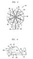
- Illustrative photogenerator 504is a diode array consisting of eight long wavelength diodes 506 connected in series. Diode arrays consisting of a greater or lesser number of diodes may suitably be used, and, for a given illumination power, will generate a correspondingly greater or lesser voltage than photogenerator 504. In some embodiments, the diode array has a circular geometry that provides a high fill factor and is complementary in shape to beam spot 578, which provides the illumination that powers photogenerator 504.
- the perimeter of photogenerator 504defines a polygon, wherein the base of each of the larger triangularly-shaped regions 582 defines a segment of the polygon.
- Larger triangularly-shaped regions 582are of one conductivity type (e.g. , "n"), and smaller triangularly-shaped regions 584 are of the other (e.g. , "p").
- Smaller triangularly-shaped regions 584are the p-i-n junction regions of each diode 580.
- diodes 580 of the arrayare serially connected. This is effected by electrical interconnections 586 that connect the n region of one diode to the p region of a first adjacent diode, and connect the p region of the one diode to the n region of a second adjacent diode. Electrical connections 588 and 590 deliver the voltage generated by photogenerator 504 to contact pads 592 and 594. Electrical interconnections (not shown in FIG. 5; shown as interconnections 108 and 106 in FIG. 1) electrically connect the photogenerator to the MEMS switch.
- FIG. 6depicts a cross section through one of the p-i-n photodiodes of photogenerator 504 through the section line designated "S" in FIG. 5.
- the photodiodecomprises five layers, patterned as depicted, that are deposited on a substrate 602.
- Substrate 602is an insulating or semi-insulating material, such as iron-doped indium phosphide (InP).
- the photodiodehas the following structure.
- the first deposited layer 604is the n-layer of the p-i-n structure and consists of silicon-doped InGaAs.
- Layer 606is a "stop etch" layer, such as, for example, undoped InP.
- Layer 608is an absorbing layer and consists of intrinsic InGaAs.
- P-layer 610comprising zinc-doped InP, must be substantially transparent at the operating wavelength of the device, typically 1.3 to 1.55 microns.
- P+ contact layer 612is zinc-doped InGaAs.
- Region 616is an interconnect, typically gold, to the adjacent n-contact (see FIG.
- region 614is a p contact metal to improve contact with p+ contact layer 612.
- Region 620is a n-contact metal to improve contact with n-layer 604.
- Region 622is an interconnect, typically gold, to the adjacent p-contact (see FIG. 5).
- improved lightwave systems and networksincorporate the aforedescribed light-actuated micromechanical photonic switch. Two of such illustrative systems are described below.
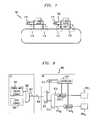
- FIG. 7depicts an improved ring network 700 in accordance with an illustrative embodiment of the invention.
- Ring network 700includes a plurality of nodes, two of which, nodes 702 and 704, are shown. It is a property of a ring network that if one node within the network goes "off-line,” the whole network goes off-line, unless the off-line node can be bypassed. As such, ring network designs typically have failsafe provisions that allow a node to be bypassed. The present light-actuated micromechanical photonic switch can be used to implement such a failsafe.
- a light-actuated micromechanical photonic switchis provided at each node within the network.
- the switches for the nodes 702 and 704are depicted in FIG. 7.
- the light actuated micromechanical photonic switch at node 702comprises MEMS switches 710 and 712 and photogenerator 714.
- the light-actuated micromechanical photonic switch at node 704comprises MEMS switches 714 and 716 and photogenerator 718.
- a nodesuch as node 702
- an optical signalis sent over fiber 706 to power photogenerator 714.
- the photogeneratorgenerates a voltage that is delivered, over electrical interconnection 708, to MEMS switches 710 and 712.
- the MEMS switches, such as switches 710 and 712,are configured such that when they are energized or actuated by the voltage generated by photogenerator 714, node 702 is in optical communication with the ring.
- a nodesuch as node 704
- its associated photogeneratorno longer receives the optical power signal. Consequently, electrical output from photogenerator 718 ceases.
- the MEMS switchessuch as switches 714 and 716, are configured such that connection to associated node ( i.e. , node 704) fails, and the node is bypassed.
- FIG. 8depicts a passive optical network 800 in accordance with an illustrative embodiment of the invention incorporating light-actuated micromechanical photonic switches for controlling data delivery to a plurality of optical network units.
- An optical beam for powering photogenerator 812, and an optical control signal for controlling controller 816, collectively identified as signal 802,are multiplexed with a data signal 804 in multiplexer 806 at central office CO.
- Data signal 804is a wavelength-division-multiplexed (WDM) signal having data intended for a plurality of optical network units ONU 1 ... ONU N , ( e.g. , homes, businesses, etc. ) modulated onto a plurality of spectral components (i.e., wavelengths) comprising the WDM signal.
- Multiplexed signal 807 from multiplexer 806is carried over fiber 808 to remote node RN.
- Fiber 808could be a very long run, as much as about 200 km, assuming a 100 mW (20 dBm), 1550 nm light source and 0.25 dB/km fiber loss.
- the optical power and control signalsare demultiplexed from the data signals and delivered to photogenerator 812.
- photogenerator 812generates a voltage, which is delivered to controller 816.
- the data signalis demultiplexed in demultiplexer 814 into a number, N, of data signals 816 1 ... 816 N intended for optical network units ONU 1 ... ONU N .
- MEMS switches 818 1 ... 818 Nactuated according to the control signal being processed by controller 816, control the information signal flow to each optical network unit.
- a passive optical networksuch as the network 800
- a passive optical networkcan be configured in a variety of ways.
- a plurality of light-actuated photonic switchescan be substituted therefor, such that a different photogenerator is associated with each of the MEMS switches 818 1 ... 818 N .
- Such an embodimentavoids using controller 816.
- modulationcan be used, as appropriate, instead of multiplexing.
Landscapes
- Physics & Mathematics (AREA)
- General Physics & Mathematics (AREA)
- Optics & Photonics (AREA)
- Engineering & Computer Science (AREA)
- Microelectronics & Electronic Packaging (AREA)
- Mechanical Light Control Or Optical Switches (AREA)
- Switches Operated By Changes In Physical Conditions (AREA)
- Optical Communication System (AREA)
Abstract
Description
The present application claims priority of Provisional Application60/058,465 filed September 10, 1997 entitled "Micromechanical PhotonicSwitch."
The present invention relates generally to photonic switches, and moreparticularly to a light-actuated photonic switch and systems incorporating same.
"Active" lightwave circuits or networks typically include electrical orelectromechanical switches that can cause a change in state in the network. Sucha change in state is used, for example, to control information flow throughout thenetwork. The switches used in such circuits require power for actuation, whichis typically supplied by external electrical sources over copper wire. Terminals,repeaters and remote node sites in the lightwave circuit must therefore be wiredso that power can be delivered to switches resident at such locations.
In many networks, providing electrical service in the aforedescribedmanner is impractical or too costly. Moreover, due to the presence of activedevices (e.g., the switches), field-deployed active lightwave circuits are likely toexperience reliability problems and high maintenance costs. Passive lightwavesystems are an alternative; unfortunately, such passive systems tend to incuradded complexity at terminal sites to compensate for the limited functionalityoutside the terminal sites.
Optically-powered circuits can enhance the functionality of an otherwisepassive optical system. In such circuits, power is supplied by an optical beamrather than an external electrical source. In some optically-powered circuits, the optical beam powers a photogenerator that produces a current/voltage to drive anelectromechanical or electrooptical device. For example, a micro power steppermotor switch powered by an indium gallium arsenide (InGaAs) photogeneratorhas been remotely actuated through 100 km of transmission fiber.See, Dentai etal., "High-Voltage (2.1V) Integrated InGaAS Photo- generator," v. 33, no. 8,Elect. Lett., pp. 718-19, 1997; and U.S. Pat. No. 5,714,773 to Burrows et al.
The photogenerators used in such lightwave circuits can be categorizedby the wavelength of the illuminating beam. Short wave photogenerators arepowered by light having a wavelength less than about 950 nanometers (nm), andlong wave photogenerators are powered by light having a wavelength greaterthan about 1200 nm. Short wave photogenerators are capable of generating morecurrent and voltage than long wave photo generators. To satisfy the non-negligiblecurrent and voltage requirements of the electrical andelectromechanical devices used in prior art optically-powered circuits, shortwave photogenerators are typically used.
Unfortunately, the "short" wavelength light that powers short wavephotogenerators is subject to significantly higher attenuation in optical fiber thanthe "long" wavelength light that powers long wave photogenerators. As a result,a fiber run to a remote node at which a short wave photogenerator and switch arelocated is typically limited to a significantly shorter length than if a long wavephotogenerator was present at the node. To extend the length of the fiber run, ahigher power optical beam must be launched into the fiber. Aside from theincreased power requirements associated with such a higher power beam, there isan increased likelihood and severity of cross talk between the power beam andthe information-carrying optical signals being delivered to the node. In additionto the aforementioned drawbacks, prior art active lightwave circuits typicallysuffer from a relatively low bandwidth and long switching times.
The art would thus benefit from an optically-powered circuit that useslong wave photogenerators to provide power for actuating switches and the like.
In one embodiment, an article comprising a light-actuated photonicswitch includes a long wave photogenerator that powers a micro-electromechanicalsystems (MEMS) switch having very low voltagerequirements. The MEMS switch incorporates a device that is mechanicallylinked to an actuator. In one embodiment, the device is a reflector that reflectsan optical signal incident thereon. The reflector of the MEMS switch ispositioned in a gap that separates source and destination optical fibers or otheroptical transmission media.
In operation, an optical beam is delivered to the long wavephotogenerator. When illuminated, the photogenerator generates a relatively lowvoltage, which is conducted to the actuator of the MEMS switch. With theapplication of that low voltage, which is typically less than 5 volts and as low asabout 1 volt, the mechanically-linked reflector is moved into the path of anoptical signal traveling from the source fiber into the gap. The optical signalcontacts the reflector and, in one embodiment, is reflected into the source fiber.In this manner, the optical signal is prevented from crossing the gap to thedestination fiber.
Being electrostatically-driven devices, most MEMS switches operateusing negligible average current, but non-negligible voltage. The presentinventors recognized that if a low-voltage MEMS switch could be developed, itcould be powered by a long wave photogenerator, avoiding some of thedrawbacks of prior art active lightwave circuits. Such a low-voltage MEMSswitch is described herein. Active lightwave circuits utilizing the present lightactuated photonic switch may realize an increase in the length of fiber spans toremote nodes of about fifty to one hundred percent over the prior art.
FIG. 1 depicts a schematic of a light-actuated photonic switch inaccordance with an illustrative embodiment of the present invention.
FIG. 2 depicts an illustrative MEMS structure for use in conjunctionwith the switch of FIG. 1.
FIG. 3a depicts an illustrative suspension element for use in conjunctionwith the MEMS structure of FIG. 2.
FIG. 3b depicts the suspension element in a deformed state.
FIG. 4a depicts the MEMS structure of FIG. 2 in a quiescent state.
FIG. 4b depicts the MEMS structure of FIG. 2 in an energized oractuated state.
FIG. 5 depicts an illustrative photogenerator for use in conjunction withthe switch of FIG. 1.
FIG. 6 depicts a cross section of the illustrative photogenerator of FIG.5.
FIG. 7 depicts a ring network in accordance with an illustrativeembodiment of the invention incorporating light-actuated photonic switches as afailsafe.
FIG. 8 depicts a passive optical network in accordance with anillustrative embodiment of the invention incorporating light-actuated photonicswitches for controlling data delivery to a plurality of optical network units.
FIG. 1 depicts a light-actuatedphotonic switch 100 in accordance withan illustrative embodiment of the present invention. Switch 100 includes aphotogenerator chip 102 having aphotogenerator 104, and aswitch chip 122having micro-electromechanical systems (MEMS)structure 124 configured toprovide a switching function (hereinafter "MEMS switch").Photogenerator 104is advantageously a long wave photogenerator, defined herein as aphotogenerator powered by an optical beam having a wavelength greater thanabout 1200 nm.Photogenerator 104 is electrically connected toMEMS switch 124 viaelectrical leads photogenerator 104 and theMEMS switch 124 are fabricated on different chips in the illustrated embodiment, it is known in the art how to monolithically integrate those twodevices. As such, in an alternative embodiment, the photogenerator and MEMSswitch are integrated on a single chip.
With continuing reference to FIG. 1,MEMS switch 124 comprises adevice 130 that is mechanically linked, vialinkage 128, to anactuator 126.Device 130 is disposed in agap 136 between a sourceoptical transmission media 132a and a destinationoptical transmission media 132b. As a function of theoperation ofactuator 126,device 130 is moved into and out of the path of anoptical signal 134 exitingsource fiber 132a.
The optical transmission media can be any one of a variety of materialssuitable for guiding an optical signal, such as, for example, slab waveguides,optical fibers and the like. For ease of exposition, such optical transmissionmedia is hereinafter collectively referred to as a "fiber" or an "optical fiber" inboth this Detailed Description and the Claims.Gap 136 is sized to receivedevice 130, but, in the absences of lenses, should be kept relatively small due tothe finite divergence of the optical signal as it leavessource fiber 132a. A gap ofabout 20 microns has been found to be suitable. It will be appreciated that if oneor more lenses are disposed withingap 136, the size of the gap will typically besubstantially larger.
In operation, anoptical fiber 110 delivers anoptical beam 112 tophotogenerator 104. When illuminated bybeam 112,photogenerator 104generates a voltage. The voltage generated byphotogenerator 104 is conducted,viaelectrical leads MEMS structure 124. Withthe application of that voltage toactuator 124,reflector 130 is moved, vialinkage 128, into the path ofsignal 134 fromsource fiber 132a. In this manner,optical signal 134 is prevented from crossinggap 136 todestination fiber 132b.In alternate embodiments,optical signal 134 may be partially attenuated byreflector 130, or a characteristic ofsignal 134 other than signal strength may bealtered, depending upon the specific implementation ofreflector 130. Theoperation of the MEMS switch is described in further detail later in thisSpecification in conjunction with a discussion of FIGS. 4a and 4b.
Referring to FIG. 2,actuator 225 consist of amovable plate 226 that issuspended bysuspension elements 240 above an electrode 202 (not shown)located underneath the movable plate. Bothmovable plate 226 andelectrode 202 are conductive. In some embodiments,electrode 202 is formed from a layerof conductive material disposed onsubstrate 200 beneathmovable plate 226.Such an electrode is referred to herein as a "discrete" electrode. In one of suchembodiments, the layer of conductive material comprises polysilicon. In someembodiments in whichsubstrate 200 is conductive, the substrate itself serves aselectrode 202. Moreover, in still other embodiments, ifsubstrate 200 is nonconductive, it can be doped to render it suitably conductive so that it canfunction aselectrode 202. Reference herein to "electrode 202" is intended toencompass any of the aforementioned implementations.
It will be appreciated that to prevent shorting,movable plate 226 mustnot contactelectrode 202. In one embodiment whereinelectrode 202 is adiscrete electrode, the electrode has holes patterned in it extending through to anunderlying nonconductive layer (e.g., the substrate). Protrusions or spikesdepend from the "under surface" of movable plate 226 (i.e., the surface of themovable plate facing underlying electrode 202). Such protrusions extenddownwardly a distance from the under surface ofmovable plate 226. The holesinelectrode 202 are aligned to receive the protrusions.
Whenmovable plate 226 moves towardselectrode 202 under appliedvoltage, the holes inelectrode 202 receive the protrusions. The protrusions havea diameter appropriate for being received by the holes without contacting theelectrode material defining the perimeter of the holes. Moreover, the length of the protrusions is greater than the thickness ofelectrode 202. Thus, whenreceived by the holes, the protrusions contact the nonconductive layer disposedunderneathelectrode 202 before the undersurface ofmovable plate 226contactselectrode 202. Such contact between the ends of the protrusions and thenonconductive layer stops the downward motion ofmovable plate 226 before itshorts againstelectrode 202. Protrusions having a length of about 0.75 micronsare suitable for use with an electrode having a thickness of about 0.5 microns.
In embodiments wherein the substrate (doped or undoped) serves aselectrode 202, a thin layer of nonconductive material, such as silicon nitride, isadvantageously disposed overelectrode 202. The nonconductive layer preventsmovable plate 226 from contactingelectrode 202 as the movable plate movesdownwardly under applied voltage.
In the illustrated embodiment,suspension elements 240 are realized as"springs" that depend fromsupports pads 242. Further detail of the illustratedembodiment of such suspension elements is provided in FIGS. 3a and 3b.
As shown in FIG. 3a, suspension elements 240 (one of which isdepicted) have an elongated U-shaped configuration (when supportedmovableplate 226 is in a neutral position).Member 344 depending fromfirst leg 346 ofsuspension elements 240 is connected to supportpad 242.Member 354depending fromfirst end 352 ofsecond leg 350 is mechanically connected tomovable plate 226, shown in partial section.
As depicted in FIG. 3b,second leg 350 moves downwardly following themovement ofmovable plate 226 as the plate is drawn towards underlyingelectrodes 202 (not shown).Second leg 350 drawsfirst leg 346 downwardlywith it. About one half of the distance through whichplate 226 drops towardunderlying electrodes 202 is accommodated by flexion insecond leg 350, andthe other half is accommodated by flexion infirst leg 346. Energy is stored insuspension element 240 as thelegs plate 226 towardselectrodes 202 and away from its neutral position is removed, the energy stored insuspension element 240 is released, returningplate 226, andfirst andsecond legs
Returning to FIG. 2,linkage 228 comprisesbeam 260 that rests onfulcrum 266 that allowsbeam 260 to "teeter" in the manner of a bascule or "seesaw."Fulcrum 266 functionally "divides"beam 260 into two portions:firstportion 262 andsecond portion 264. In the illustrated embodiment,fulcrum 266is realized byarms 270 that depend from the sides ofbeam 260.Arms 270 reston, but are not attached to, fulcrum supports 268. As such,arms 270 are free topivot or rock such that asfirst portion 262 ofbeam 260 is driven downwardly,such as by downward movement ofmovable plate 226, second portion ofbeam 260 moves upwardly, away fromsubstrate 200.
In the illustrated embodiment,arms 270 are thus bifunctional; they are pivot elements and also function as torsional springs. In other embodiments,separate elements provide those two functions. For example, in one embodiment(not shown), the arms extend no further than fulcrum supports 268 upon whichthey rest. When so implemented, the arms function simply as pivots. A separatepair of torsional springs, configured, for example, in the manner ofsprings 240,are attached to the sides ofbeam 260near end 278 ofsecond portion 264 ofbeam 260.
Operation ofillustrative MEMS switch 224 is described with reference toFIGS. 4a and 4b. FIG. 4a depicts a simplified version ofMEMS switch 224 in aneutral or quiescent state. In such a quiescent state,reflector 230 is located offof the optical axis defined by fiber core 470 (i.e., optical axis A-A of FIG. 2),such that it does not intercept an optical signal traveling through the fiber core.FIG. 4b depictsMEMS switch 224 in an actuated state. As voltage is appliedacrossplate 226 andelectrode 202, an electrostatic attraction is developedtherebetween. Such an attraction causesmovable plate 226 to move downwardlytowardselectrodes 202, decreasing the separation distanceS therebetween.Firstportion 262 ofbeam 260, which abuts under-surface 227 ofmovable plate 226,is driven downwardly along withmovable plate 226. Due tofulcrum 226,second portion 264 ofbeam 260 moves upwardly away fromsubstrate 200 inresponse to the downward movement offirst portion 262. The upwardmovement ofsecond portion 264 ofbeam 260 moves reflector 230 into theoptical axis defined byfiber core 470, thereby intercepting an optical signaltraveling therethrough. The location offulcrum 266 along the length ofbeam 260 is suitably adjusted to provide a desired amount of vertical movement at theend ofsecond portion 264 of the beam such thatreflector 230 intersects the optical axis whenactuator 225 is energized.
In the embodiment illustrated in FIG. 4a,reflector 230 is depicted asbeing located beneathfiber core 470 in the quiescent position, moving into thepath of the fiber core upon actuation. In other embodiments,reflector 230 islocated in the path of thefiber core 470 in the quiescent position, and moves"above" the fiber core upon actuation.
It was previously noted that MEMS switches for use in conjunction areadvantageously actuated by very low voltages to realize the benefits of thepresent invention. It has been found that with certain modifications to a"standard" MEMS switch design, a switch actuable at very low voltage (andnegligible current) can be fabricated. Such modifications are described below.
In a first modification,suspension elements 240 that suspendmovableplate 226 must be "soft." As the term is used herein, a "soft" suspension elementhas a spring constant within the range of about 0.25 to 0.5 Newtons/meter. Bycontrast, the spring constant for suspension elements used in a typical MEMSdevice is on the order of about 10 N/m. To fabricate such a "soft" suspensionelement, the elements are typically lengthened. As a guideline, the springconstant is assumed to be inversely proportional to the third power of the lengthof the spring element (i.e., K ∝ (1/L3). For a torsional element, the springconstant is assumed to be inversely proportional to the first power of the lengthof the torsional element (i.e.,K ∝ (1/L).
In a second modification, themovable plate 226 is advantageouslysufficiently large such that substantial flexion occurs during actuation.Regarding such plate flexion, asmovable plate 226 is drawn towardselectrode 202, it deforms substantially such as voltage is first applied, only a small regionof the movable plate (or protrusions depending therefrom) contacts anunderlying nonconductive surface. The region that makes such "initial" contactis typically the region of the plate furthest from the suspension elements (and theportion ofbeam 260 underlying movable layer 226). The contact region"propagates" in a "zip-lock" fashion away from the initial contact point. A large electrostatic force of attraction is generated with surprisingly low voltage whensuch flexion is provided inmovable plate 226. Regarding plate size, a movableplate of at least about 300 microns x 300 microns x 1.5 microns thickness hasbeen found to be adequate in this regard.
Additionally,electrode 202 is advantageously realized using the substrateas the electrode with an overlying layer of silicon nitride. Such an arrangementhas been found to typically result in lower actuation voltages than switches usingdiscrete electrodes. Moreover,movable layer 226 advantageously comprisesonly a single polysilicon layer (the "POLY2" layer of MCNC's three-polysilicon-layermicromachining process described below), while in "standard"(i.e., higher voltage) MEMS switches used in other applications, the movablelayer often comprises two layers of polysilicon.
Technology for fabricating a MEMS switch, such asMEMS switch 226in accordance with the present teachings is available from a variety of sources,such as, for example, the MEMS Microelectronics Center of North Carolina(MCNC). One of the technologies offered by MCNC is a three-polysilicon-layersurface micromachining process. In that process, a silicon wafer is first coveredwith an insulating silicon nitride layer. Three separate layers of polysilicon,POLY0, POLY1 and POLY2 are then deposited and patterned. A layer of oxide(e.g., phosphosilicate glass "PSG") is sandwiched between the first (POLY0)and second (POLY1) layer, as well as between the POLY1 layer and theuppermost (POLY2) layer. By virtue of the aforementioned sacrificial oxidelayers, the POLY1 and POLY2 are "releasable" (by etching away such oxidelayers) and so can be used to form mechanical structures. The lowermostPOLY0 layer is non-releasable and is used for patterning address electrodes andlocal wiring on the insulating silicon nitride layer. The polysilicon layersPOLY0, POLY1 and POLY2 have nominal thicknesses of 0.5, 2.0 and 1.5microns, respectively. Optionally, a layer of gold, nominally about 0.5 micronsin thickness, can be deposited on the POLY2 layer.
The polysilicon and oxide layers are individually patterned as desired, and unwanted material from each layer is removed by reactive ion etching beforethe next layer is added. After all layers are patterned, the POLY1 and POLY2layers are released, as required, using HF to etch away the sacrificial oxidelayers. After release, the patterned POLY1 and POLY2 layers are free to move,and assembly, if not accomplished during fabrication steps, can proceed.
During "active" assembly, the various elements of the MEMS device aremoved into position after the various elements of the MEMS device are formed.More particularly, various plates are moved from an initial position, typically inthe plane of the substrate, to a final and typically out-of-the-substrate-planeposition. Plates can be moved into final position with, for example, amicropipette. MEMS device that are actively assembled are typically comprisedof at least a few "hinged plates." Such hinged plates are rotatable about theirhinge. As formed, such hinged plates lie flat on the surface of the substrate.Assembly typically requires rotating such a plate about its hinges out of theplane of the substrate. Some plates will be rotated by ninety degrees, and othersby a lesser amount. Forming such hinged plates is known in the art. See, forexample, Pister et al., "Microfabricated Hinges," vol. 33, Sensors and ActuatorsA, pp. 249-356, 1992. See also, assignee's co-pending patent applications"Micro Machined Optical Switch," filed May 15, 1997 as serial no. 08/856,569and "Methods and Apparatus for Making a Microdevice," filed May 15, 1997 asserial no. 08/056,565, both of which applications are incorporated by referenceherein.
As an alternative to active assembly, the present MEMS switches canadvantageously be "passively" self assembled. In passive assembly, the variouselements of the MEMS device are moved into their working positions during theprocess of fabrication. One way to accomplish such passive assembly is todeposit a layer of material having a high intrinsic stress on top of a polysiliconbeam or plate that is supported at only one end (i.e., cantilevered) In theaforedescribed MCNC process, the gold layer optionally deposited on thePOLY2 layer can be deposited such that it possesses a high intrinsic stress. For example, in one embodiment, the material serving as an adhesion layer (typicallyrequired) between the polysilicon and the gold is chromium. A high intrinsicstress is associated with the chromium layer. When the sacrificial oxide layer isetched away to release the beam or plate, the chromium layer contracts tominimize strain. Upon such contraction, an upwardly-directed force is impartedto the free end of beam or plate, causing it to warp in an "upwards" direction.Such upward movement can be used to move structures into their workingpositions. See, for example, assignee's co-pending patent application "Self-AssemblingMicro-Mechanical Device," filed December 22, 1997 as serial no.08/997175, which application is incorporated herein by reference.
Referring again to FIG. 1, the voltage that drivesactuator 126 ofMEMS switch 124 is generated byphotogenerator 104. An illustrative embodiment of aphotogenerator 504 suitable for use in conjunction with the present invention isdepicted in FIG. 5.
Referring again to FIG. 1, the voltage that drives
The perimeter ofphotogenerator 504 defines a polygon, wherein the baseof each of the larger triangularly-shapedregions 582 defines a segment of thepolygon. Larger triangularly-shapedregions 582 are of one conductivity type(e.g., "n"), and smaller triangularly-shapedregions 584 are of the other (e.g.,"p"). Smaller triangularly-shapedregions 584 are the p-i-n junction regions ofeachdiode 580.
As previously indicated,diodes 580 of the array are serially connected.This is effected byelectrical interconnections 586 that connect the n region ofone diode to the p region of a first adjacent diode, and connect the p region of the one diode to the n region of a second adjacent diode.Electrical connections photogenerator 504 to contactpads interconnections
FIG. 6 depicts a cross section through one of the p-i-n photodiodes ofphotogenerator 504 through the section line designated "S" in FIG. 5. In theillustrated embodiment, the photodiode comprises five layers, patterned asdepicted, that are deposited on asubstrate 602.Substrate 602 is an insulating orsemi-insulating material, such as iron-doped indium phosphide (InP).
In one embodiment, the photodiode has the following structure. The firstdepositedlayer 604 is the n-layer of the p-i-n structure and consists of silicon-dopedInGaAs.Layer 606 is a "stop etch" layer, such as, for example, undopedInP.Layer 608 is an absorbing layer and consists of intrinsic InGaAs. P-layer 610, comprising zinc-doped InP, must be substantially transparent at theoperating wavelength of the device, typically 1.3 to 1.55 microns.P+ contactlayer 612 is zinc-doped InGaAs. An insulator, such as polyimide, surrounds thelayers 604-612.Region 616 is an interconnect, typically gold, to the adjacent n-contact(see FIG. 5), andregion 614 is a p contact metal to improve contact withp+ contact
layer 612.Region 620 is a n-contact metal to improve contact with n-layer 604.Region 622 is an interconnect, typically gold, to the adjacent p-contact (see FIG.5).
Further description of a photodiode array suitable for use in conjunctionwith the present invention is provided in U.S. Pat. No. 5,714,773 by Burrows etal. entitled "Photodiode Array for Remotely Powered Lightwave Networks,"issued February 3, 1998, and incorporated by reference herein.
In further embodiments of the present invention, improved lightwavesystems and networks incorporate the aforedescribed light-actuatedmicromechanical photonic switch. Two of such illustrative systems are described below.
FIG. 7 depicts animproved ring network 700 in accordance with anillustrative embodiment of the invention.Ring network 700 includes a pluralityof nodes, two of which,nodes
A light-actuated micromechanical photonic switch is provided at eachnode within the network. The switches for thenodes node 702comprises MEMS switches 710 and 712 andphotogenerator 714. The light-actuatedmicromechanical photonic switch atnode 704 comprises MEMSswitches 714 and 716 andphotogenerator 718.
When a node, such asnode 702, is on-line, an optical signal is sent overfiber 706 topower photogenerator 714. The photogenerator generates a voltagethat is delivered, overelectrical interconnection 708, toMEMS switches switches photogenerator 714,node 702 is in optical communication with the ring.
When a node, such asnode 704, is off-line, its associated photogeneratorno longer receives the optical power signal. Consequently, electrical outputfromphotogenerator 718 ceases. In the absence of an actuating voltage, theMEMS switches, such asswitches
FIG. 8 depicts a passiveoptical network 800 in accordance with anillustrative embodiment of the invention incorporating light-actuatedmicromechanical photonic switches for controlling data delivery to a plurality ofoptical network units.
An optical beam for poweringphotogenerator 812, and an optical controlsignal for controllingcontroller 816, collectively identified assignal 802, aremultiplexed with adata signal 804 inmultiplexer 806 at central office CO. Datasignal 804 is a wavelength-division-multiplexed (WDM) signal having dataintended for a plurality of optical network units ONU1 ... ONUN, (e.g., homes,businesses,etc.) modulated onto a plurality of spectral components (i.e.,wavelengths) comprising the WDM signal.Multiplexed signal 807 frommultiplexer 806 is carried overfiber 808 to remote node RN.Fiber 808 could bea very long run, as much as about 200 km, assuming a 100 mW (20 dBm), 1550nm light source and 0.25 dB/km fiber loss.
At remote node RN, the optical power and control signals aredemultiplexed from the data signals and delivered tophotogenerator 812. Inresponse,photogenerator 812 generates a voltage, which is delivered tocontroller 816. The data signal is demultiplexed indemultiplexer 814 into anumber,N, of data signals 8161 ... 816N intended for optical network units ONU1... ONUN. MEMS switches 8181 ... 818N, actuated according to the control signalbeing processed bycontroller 816, control the information signal flow to eachoptical network unit.
It will be appreciated that a passive optical network, such as thenetwork 800, can be configured in a variety of ways. For example, rather than using asingle photogenerator 812 and acontroller 816, a plurality of light-actuatedphotonic switches can be substituted therefor, such that a differentphotogenerator is associated with each of the MEMS switches 8181 ... 818N.Such an embodiment avoids usingcontroller 816. Moreover, modulation can beused, as appropriate, instead of multiplexing.
It is to be understood that the embodiments described herein are merelyillustrative of the many possible specific arrangements that can be devised inapplication of the principles of the invention. Other arrangements can be devisedin accordance with these principles by those of ordinary skill in the art withoutdeparting from the scope and spirit of the invention. It is therefore intended that such other arrangements be included within the scope of the following claimsand their equivalents.
Claims (11)
- An article including a light-actuated photonic switch, said switchcomprising:wherein,a photogenerator that generates a voltage when illuminated by an opticalbeam; anda first micro electromechanical systems (MEMS) device operable toprovide a switching function, said MEMS device being electrically connected tothe photogenerator and comprising:an actuator including a movable plate disposed in spaced andsuperposed relation to a fixed electrode, said actuatorbeing actuated by applying the voltage generated by thephotogenerator to the movable plate and the fixedelectrode;a reflector operable to affect a characteristic of an optical signalincident thereon; anda linkage mechanically connecting the actuator to the reflector,when the actuator is actuated, the reflector is moved causing a change instate of the light-actuated photonic switch.
- The article of claim 1, wherein the voltage is less than about 5volts.
- The article of claim 2, wherein the photogenerator comprises aplurality of series-connected photodiodes operable to generate a voltage whenexposed to light having a wavelength greater than about 1200 nanometers.
- The article of claim 3, wherein the photodiodes comprising thephotogenerator are arranged in a circular geometry.
- The article of claim 4, wherein the movable plate is supported byresilient springs having a spring constant less than about 0.5 Newtons per meter.
- The article of claim 1, wherein the linkage is a beam, and furtherwherein the beam is functionally separated into a first and a second portion by afulcrum, wherein part of the first portion of the beam underlies and abuts themovable plate, and further wherein the reflector is mechanically connected to thesecond portion of the beam and disposed between two optical fibers.
- The article of claim 6, wherein the fulcrum comprises armsdepending from sides of the beam, and fulcrum supports upon which said armsfreely rest.
- The article of claim 7, further comprising a torsional spring forproviding a restoring force to the beam.
- The article of claim 8, wherein the torsional spring comprises saidarms depending from sides of the beam, wherein the arms extend laterallybeyond the fulcrum supports and are fixed to arm supports.
- The article of claim 1, wherein the article is a network comprisinga plurality of optically communicating nodes arranged in a ring architecture,each node including two of the MEMS device, which two MEMS devices areactuated by at least one photogenerator, wherein,in a first state of the network, a portion of light traveling through eachnode powers the one photogenerator associated therewith, said photogeneratorgenerating a voltage that actuates the two MEMS devices, which MEMS devicesare configured, in the actuated state, to receive the light and direct it to theassociated node, andin a second state of the network, the portion of light travelling through at least one of the nodes is not available to power the one photogenerator such thatthe two MEMS devices at the one node are unactuated, in which unactuatedcondition said two MEMS devices receive the light intended for the one nodeand cause said light to bypass the one node.
- The article of claim 1, wherein the article is a passive opticalnetwork comprising:a central office at which an optical beam, an optical control signal and amultiplexed optical data signal comprising a plurality of data signals aremultiplexed into a multiplexed optical signal;an optical fiber for delivering the multiplexed optical signal to a remotenode; andthe remote node, wherein the remote node consists of:the light-actuated photonic switch including additional MEMSdevices such that there is one MEMS device for each datasignal in the multiplexed optical data signal;a first demultiplexer for demultiplexing the optical beam and theoptical control signal from the multiplexed optical datasignal, which demultiplexed optical beam and opticalcontrol signal is delivered to the photogenerator of thelight-actuated photonic switch;a second demultiplexer that receives and demultiplexes themultiplexed optical data signal from the firstdemultiplexer into the plurality of data signals eachcharacterized by a unique wavelength, wherein each ofsaid demultiplexed data signals are placed in opticalcommunication with a MEMS device; anda controller, wherein,when the photogenerator is illuminated by the optical beam and opticalcontrol signal, a voltage is generated that causes the controller to selectively actuate the MEMS switches to control delivery of the data signals to opticalnetwork units according to wavelength.
Applications Claiming Priority (5)
| Application Number | Priority Date | Filing Date | Title |
|---|---|---|---|
| 1997-02-13 | |||
| US5846597P | 1997-09-10 | 1997-09-10 | |
| US58465P | 1997-09-10 | ||
| US09/138,686US6075239A (en) | 1997-09-10 | 1998-08-24 | Article comprising a light-actuated micromechanical photonic switch |
| US138686 | 1998-08-24 |
Publications (2)
| Publication Number | Publication Date |
|---|---|
| EP0902538A2true EP0902538A2 (en) | 1999-03-17 |
| EP0902538A3 EP0902538A3 (en) | 1999-12-22 |
Family
ID=26737645
Family Applications (1)
| Application Number | Title | Priority Date | Filing Date |
|---|---|---|---|
| EP98307019AWithdrawnEP0902538A3 (en) | 1997-09-10 | 1998-09-01 | Article comprising a light-actuated micromechanical photonic switch |
Country Status (3)
| Country | Link |
|---|---|
| US (1) | US6075239A (en) |
| EP (1) | EP0902538A3 (en) |
| JP (1) | JPH11154447A (en) |
Cited By (24)
| Publication number | Priority date | Publication date | Assignee | Title |
|---|---|---|---|---|
| US6356377B1 (en) | 1999-11-10 | 2002-03-12 | Agere Systems Guardian Corp. | Mems variable optical delay lines |
| WO2001048532A3 (en)* | 1999-11-23 | 2002-04-11 | Nanovation Tech Inc | Integrated planar optical waveguide and shutter |
| US6389189B1 (en) | 1998-10-23 | 2002-05-14 | Corning Incorporated | Fluid-encapsulated MEMS optical switch |
| US6404942B1 (en) | 1998-10-23 | 2002-06-11 | Corning Incorporated | Fluid-encapsulated MEMS optical switch |
| DE10106699A1 (en)* | 2001-02-14 | 2002-08-29 | Leica Microsystems | Touch sensor and device for protecting a protruding component |
| US6445840B1 (en) | 1999-05-28 | 2002-09-03 | Omm, Inc. | Micromachined optical switching devices |
| US6445841B1 (en) | 1999-05-28 | 2002-09-03 | Omm, Inc. | Optomechanical matrix switches including collimator arrays |
| US6449406B1 (en) | 1999-05-28 | 2002-09-10 | Omm, Inc. | Micromachined optomechanical switching devices |
| US6453083B1 (en) | 1999-05-28 | 2002-09-17 | Anis Husain | Micromachined optomechanical switching cell with parallel plate actuator and on-chip power monitoring |
| US6487000B2 (en) | 2000-08-09 | 2002-11-26 | Stmicroelectronics S.R.L. | Microelectromechanical structure comprising distinct parts mechanically connected through a translation/rotation conversion assembly |
| US6498870B1 (en) | 1998-04-20 | 2002-12-24 | Omm, Inc. | Micromachined optomechanical switches |
| US6556741B1 (en) | 2000-10-25 | 2003-04-29 | Omm, Inc. | MEMS optical switch with torsional hinge and method of fabrication thereof |
| US6556739B1 (en) | 2001-02-13 | 2003-04-29 | Omm, Inc. | Electronic damping of MEMS devices using a look-up table |
| US6567574B1 (en) | 2000-10-06 | 2003-05-20 | Omm, Inc. | Modular three-dimensional optical switch |
| US6571029B1 (en) | 2001-02-13 | 2003-05-27 | Omm, Inc. | Method for determining and implementing electrical damping coefficients |
| US6643426B1 (en) | 1999-10-19 | 2003-11-04 | Corning Incorporated | Mechanically assisted release for MEMS optical switch |
| US6647164B1 (en) | 2000-10-31 | 2003-11-11 | 3M Innovative Properties Company | Gimbaled micro-mirror positionable by thermal actuators |
| EP1089108A3 (en)* | 1999-09-28 | 2004-01-21 | Agilent Technologies, Inc. (a Delaware corporation) | Optical switches using micromirrors in trenches and integrated optical waveguides |
| US6711318B2 (en) | 2001-01-29 | 2004-03-23 | 3M Innovative Properties Company | Optical switch based on rotating vertical micro-mirror |
| WO2004094301A1 (en)* | 2003-04-24 | 2004-11-04 | Metconnex Canada Inc. | A micro-electro-mechanical-system two dimensional mirror with articulated suspension structures for high fill factor arrays |
| US7095546B2 (en) | 2003-04-24 | 2006-08-22 | Metconnex Canada Inc. | Micro-electro-mechanical-system two dimensional mirror with articulated suspension structures for high fill factor arrays |
| EP1724624A4 (en)* | 2004-03-09 | 2008-05-07 | Fujitsu Ltd | MIRROR DEVICE, OPTICAL CONTROLLER, MIRROR CONTROL METHOD, AND MIRROR ELEMENT |
| US7432629B2 (en) | 2005-02-16 | 2008-10-07 | Jds Uniphase Corporation | Articulated MEMs structures |
| CN103618533A (en)* | 2013-12-03 | 2014-03-05 | 沈仁辉 | Switch control device based on optical fiber conduction and switch control system thereof |
Families Citing this family (71)
| Publication number | Priority date | Publication date | Assignee | Title |
|---|---|---|---|---|
| JP3912760B2 (en)* | 1999-01-20 | 2007-05-09 | 富士フイルム株式会社 | Driving method of array type light modulation element and flat display device |
| US6292281B1 (en)* | 1999-03-24 | 2001-09-18 | Tellium, Inc. | Protection for MEMS cross-bar switch |
| JP2000295030A (en)* | 1999-04-06 | 2000-10-20 | Nec Corp | High frequency device and its manufacture |
| US7388186B2 (en)* | 1999-10-28 | 2008-06-17 | Hrl Laboratories, Llc | Optically controlled MEMS devices |
| US6310339B1 (en)* | 1999-10-28 | 2001-10-30 | Hrl Laboratories, Llc | Optically controlled MEM switches |
| KR20020064909A (en) | 1999-11-23 | 2002-08-10 | 나노베이션 테크놀로지즈, 인크. | An optical switch having a planar waveguide and a shutter actuator |
| US6470108B1 (en)* | 2000-04-26 | 2002-10-22 | Tini Alloy Company | Optical switching device and method |
| US6585383B2 (en) | 2000-05-18 | 2003-07-01 | Calient Networks, Inc. | Micromachined apparatus for improved reflection of light |
| US6560384B1 (en) | 2000-06-01 | 2003-05-06 | Calient Networks, Inc. | Optical switch having mirrors arranged to accommodate freedom of movement |
| US6670208B2 (en) | 2000-06-23 | 2003-12-30 | Nec Corporation | Optical circuit in which fabrication is easy |
| US6643425B1 (en)* | 2000-08-17 | 2003-11-04 | Calient Networks, Inc. | Optical switch having switch mirror arrays controlled by scanning beams |
| WO2002021195A2 (en) | 2000-09-07 | 2002-03-14 | Terra-Op Ltd. | Method and system for ultra-fast switching of optical signals |
| US6687428B2 (en) | 2000-09-21 | 2004-02-03 | Tera Op (Usa) Inc. | Optical switch |
| US6825967B1 (en) | 2000-09-29 | 2004-11-30 | Calient Networks, Inc. | Shaped electrodes for micro-electro-mechanical-system (MEMS) devices to improve actuator performance and methods for fabricating the same |
| US6762876B2 (en)* | 2000-11-20 | 2004-07-13 | Terraop Ltd. | Optical converter with a designated output wavelength |
| US6829079B2 (en) | 2000-12-22 | 2004-12-07 | Nec Corporation | Optical path control apparatus with mirror section, and manufacturing method for the same |
| US6731833B2 (en) | 2001-01-16 | 2004-05-04 | T-Rex Enterprises Corp. | Optical cross connect switch |
| US6588208B1 (en)* | 2001-01-29 | 2003-07-08 | Technology Innovations, Llc | Wireless technique for microactivation |
| US7800639B2 (en)* | 2001-02-15 | 2010-09-21 | Joseph Dale Udy | Laser pulse image switches |
| JP3923265B2 (en)* | 2001-02-15 | 2007-05-30 | 古河電気工業株式会社 | Variable optical attenuator |
| US6717254B2 (en) | 2001-02-22 | 2004-04-06 | Tru-Si Technologies, Inc. | Devices having substrates with opening passing through the substrates and conductors in the openings, and methods of manufacture |
| US7183633B2 (en)* | 2001-03-01 | 2007-02-27 | Analog Devices Inc. | Optical cross-connect system |
| WO2002091464A1 (en)* | 2001-03-01 | 2002-11-14 | Onix Micro Systems | Optical cross-connect system |
| US6792177B2 (en) | 2001-03-12 | 2004-09-14 | Calient Networks, Inc. | Optical switch with internal monitoring |
| JP2002286968A (en)* | 2001-03-28 | 2002-10-03 | Seiko Instruments Inc | Optical functional module |
| US6859578B2 (en)* | 2001-05-18 | 2005-02-22 | Nuonics, Inc. | Fault-tolerant fiber-optical multiwavelength processor |
| US6543087B2 (en) | 2001-06-01 | 2003-04-08 | Aip Networks, Inc. | Micro-electromechanical hinged flap structure |
| KR100422037B1 (en)* | 2001-08-09 | 2004-03-12 | 삼성전기주식회사 | Variable optical attenuator of optical path conversion |
| JP3750574B2 (en) | 2001-08-16 | 2006-03-01 | 株式会社デンソー | Thin film electromagnet and switching element using the same |
| US6787916B2 (en) | 2001-09-13 | 2004-09-07 | Tru-Si Technologies, Inc. | Structures having a substrate with a cavity and having an integrated circuit bonded to a contact pad located in the cavity |
| KR100393193B1 (en)* | 2001-09-29 | 2003-07-31 | 삼성전자주식회사 | Variable optical attenuator having waveguides and MEMS actuator |
| US6751395B1 (en)* | 2001-11-09 | 2004-06-15 | Active Optical Networks, Inc. | Micro-electro-mechanical variable optical attenuator |
| US6917268B2 (en)* | 2001-12-31 | 2005-07-12 | International Business Machines Corporation | Lateral microelectromechanical system switch |
| US20050091975A1 (en)* | 2002-01-28 | 2005-05-05 | Technology Innovations, Llc | Microactivation using fiber optic and wireless means |
| KR100420954B1 (en)* | 2002-03-27 | 2004-03-02 | 한국전자통신연구원 | Otical switching device and method of manufacturing the same, and array structure thereof |
| US6665463B2 (en) | 2002-04-02 | 2003-12-16 | Tera Op, Inc. | Optical switching system |
| US6879429B2 (en)* | 2002-05-15 | 2005-04-12 | Jds Uniphase Inc. | Drive circuit for a MEMS device |
| US7040323B1 (en)* | 2002-08-08 | 2006-05-09 | Tini Alloy Company | Thin film intrauterine device |
| US6898342B2 (en)* | 2002-08-08 | 2005-05-24 | Intel Corporation | Fiber-aligning optical switch |
| US6975783B2 (en)* | 2003-02-19 | 2005-12-13 | Northrop Grumman Corporation | Switch control with light beams |
| US6993219B2 (en)* | 2003-03-13 | 2006-01-31 | Lucent Technologies Inc. | Waveguide/MEMS switch |
| DE10338108B4 (en)* | 2003-08-19 | 2013-01-24 | Minebea Co., Ltd. | Device for detecting individual moving objects of very small dimensions |
| WO2005029162A2 (en)* | 2003-09-15 | 2005-03-31 | Reveo, Inc. | Applications of light movable liquid crystal |
| US7422403B1 (en) | 2003-10-23 | 2008-09-09 | Tini Alloy Company | Non-explosive releasable coupling device |
| US7586828B1 (en) | 2003-10-23 | 2009-09-08 | Tini Alloy Company | Magnetic data storage system |
| US7116857B2 (en)* | 2003-12-08 | 2006-10-03 | Reveo, Inc. | Optomechanical switch using laser or light movable liquid crystal |
| DE102004001157A1 (en)* | 2004-01-07 | 2005-08-11 | Minebea Co., Ltd. | Device for detecting and / or characterizing individual moving objects of very small dimensions |
| US7632361B2 (en)* | 2004-05-06 | 2009-12-15 | Tini Alloy Company | Single crystal shape memory alloy devices and methods |
| US7356880B2 (en)* | 2004-07-26 | 2008-04-15 | Pentax Corporation | Hinge structure of micromirror device |
| US20060118210A1 (en)* | 2004-10-04 | 2006-06-08 | Johnson A D | Portable energy storage devices and methods |
| US7763342B2 (en)* | 2005-03-31 | 2010-07-27 | Tini Alloy Company | Tear-resistant thin film methods of fabrication |
| US7441888B1 (en) | 2005-05-09 | 2008-10-28 | Tini Alloy Company | Eyeglass frame |
| US7540899B1 (en) | 2005-05-25 | 2009-06-02 | Tini Alloy Company | Shape memory alloy thin film, method of fabrication, and articles of manufacture |
| US20080075557A1 (en)* | 2006-09-22 | 2008-03-27 | Johnson A David | Constant load bolt |
| US20080213062A1 (en)* | 2006-09-22 | 2008-09-04 | Tini Alloy Company | Constant load fastener |
| WO2008133738A2 (en) | 2006-12-01 | 2008-11-06 | Tini Alloy Company | Method of alloying reactive components |
| US8584767B2 (en) | 2007-01-25 | 2013-11-19 | Tini Alloy Company | Sprinkler valve with active actuation |
| WO2008092028A1 (en) | 2007-01-25 | 2008-07-31 | Tini Alloy Company | Frangible shape memory alloy fire sprinkler valve actuator |
| US8007674B2 (en) | 2007-07-30 | 2011-08-30 | Tini Alloy Company | Method and devices for preventing restenosis in cardiovascular stents |
| US8556969B2 (en) | 2007-11-30 | 2013-10-15 | Ormco Corporation | Biocompatible copper-based single-crystal shape memory alloys |
| US7842143B2 (en)* | 2007-12-03 | 2010-11-30 | Tini Alloy Company | Hyperelastic shape setting devices and fabrication methods |
| US8382917B2 (en)* | 2007-12-03 | 2013-02-26 | Ormco Corporation | Hyperelastic shape setting devices and fabrication methods |
| US8531082B2 (en) | 2010-08-27 | 2013-09-10 | Industrial Technology Research Institute | Actuator and method for using the same |
| US8569861B2 (en) | 2010-12-22 | 2013-10-29 | Analog Devices, Inc. | Vertically integrated systems |
| US10124197B2 (en) | 2012-08-31 | 2018-11-13 | TiNi Allot Company | Fire sprinkler valve actuator |
| US11040230B2 (en) | 2012-08-31 | 2021-06-22 | Tini Alloy Company | Fire sprinkler valve actuator |
| US9285538B2 (en) | 2012-10-23 | 2016-03-15 | Lumentum Operations Llc | Reducing temperature drift of an arrayed waveguide grating |
| US20150212273A1 (en)* | 2014-01-30 | 2015-07-30 | Adtran, Inc. | Optical fiber adapter with embedded optical attenuator |
| EP3625554A1 (en) | 2017-05-15 | 2020-03-25 | Analog Devices Global Unlimited Company | Integrated ion sensing apparatus and methods |
| US10730743B2 (en) | 2017-11-06 | 2020-08-04 | Analog Devices Global Unlimited Company | Gas sensor packages |
| US11587839B2 (en) | 2019-06-27 | 2023-02-21 | Analog Devices, Inc. | Device with chemical reaction chamber |
Family Cites Families (6)
| Publication number | Priority date | Publication date | Assignee | Title |
|---|---|---|---|---|
| DE69114692T2 (en)* | 1991-03-25 | 1996-06-20 | Ibm | Fiber optic switch with optical remote supply. |
| US5367584A (en)* | 1993-10-27 | 1994-11-22 | General Electric Company | Integrated microelectromechanical polymeric photonic switching arrays |
| US5367585A (en)* | 1993-10-27 | 1994-11-22 | General Electric Company | Integrated microelectromechanical polymeric photonic switch |
| US5714773A (en)* | 1996-10-15 | 1998-02-03 | Lucent Technologies Inc. | Photodiode array for remotely powered lightwave networks |
| US5953469A (en)* | 1996-10-29 | 1999-09-14 | Xeotron Corporation | Optical device utilizing optical waveguides and mechanical light-switches |
| US5781331A (en)* | 1997-01-24 | 1998-07-14 | Roxburgh Ltd. | Optical microshutter array |
- 1998
- 1998-08-24USUS09/138,686patent/US6075239A/ennot_activeExpired - Lifetime
- 1998-09-01EPEP98307019Apatent/EP0902538A3/ennot_activeWithdrawn
- 1998-09-10JPJP10255876Apatent/JPH11154447A/enactivePending
Cited By (27)
| Publication number | Priority date | Publication date | Assignee | Title |
|---|---|---|---|---|
| US6498870B1 (en) | 1998-04-20 | 2002-12-24 | Omm, Inc. | Micromachined optomechanical switches |
| US6526198B1 (en) | 1998-04-20 | 2003-02-25 | Omm, Inc. | Micromachined optomechanical switches |
| US6389189B1 (en) | 1998-10-23 | 2002-05-14 | Corning Incorporated | Fluid-encapsulated MEMS optical switch |
| US6404942B1 (en) | 1998-10-23 | 2002-06-11 | Corning Incorporated | Fluid-encapsulated MEMS optical switch |
| US6445841B1 (en) | 1999-05-28 | 2002-09-03 | Omm, Inc. | Optomechanical matrix switches including collimator arrays |
| US6445840B1 (en) | 1999-05-28 | 2002-09-03 | Omm, Inc. | Micromachined optical switching devices |
| US6449406B1 (en) | 1999-05-28 | 2002-09-10 | Omm, Inc. | Micromachined optomechanical switching devices |
| US6453083B1 (en) | 1999-05-28 | 2002-09-17 | Anis Husain | Micromachined optomechanical switching cell with parallel plate actuator and on-chip power monitoring |
| EP1089108A3 (en)* | 1999-09-28 | 2004-01-21 | Agilent Technologies, Inc. (a Delaware corporation) | Optical switches using micromirrors in trenches and integrated optical waveguides |
| US6643426B1 (en) | 1999-10-19 | 2003-11-04 | Corning Incorporated | Mechanically assisted release for MEMS optical switch |
| EP1099972A3 (en)* | 1999-11-10 | 2004-05-19 | Lucent Technologies Inc. | Variable optical delay lines with a micro electro-mechanical system |
| US6356377B1 (en) | 1999-11-10 | 2002-03-12 | Agere Systems Guardian Corp. | Mems variable optical delay lines |
| WO2001048532A3 (en)* | 1999-11-23 | 2002-04-11 | Nanovation Tech Inc | Integrated planar optical waveguide and shutter |
| US6487000B2 (en) | 2000-08-09 | 2002-11-26 | Stmicroelectronics S.R.L. | Microelectromechanical structure comprising distinct parts mechanically connected through a translation/rotation conversion assembly |
| US6567574B1 (en) | 2000-10-06 | 2003-05-20 | Omm, Inc. | Modular three-dimensional optical switch |
| US6556741B1 (en) | 2000-10-25 | 2003-04-29 | Omm, Inc. | MEMS optical switch with torsional hinge and method of fabrication thereof |
| US6647164B1 (en) | 2000-10-31 | 2003-11-11 | 3M Innovative Properties Company | Gimbaled micro-mirror positionable by thermal actuators |
| US6711318B2 (en) | 2001-01-29 | 2004-03-23 | 3M Innovative Properties Company | Optical switch based on rotating vertical micro-mirror |
| US6571029B1 (en) | 2001-02-13 | 2003-05-27 | Omm, Inc. | Method for determining and implementing electrical damping coefficients |
| US6556739B1 (en) | 2001-02-13 | 2003-04-29 | Omm, Inc. | Electronic damping of MEMS devices using a look-up table |
| DE10106699C2 (en)* | 2001-02-14 | 2003-11-27 | Leica Microsystems | Touch sensor and device for protecting a protruding component |
| DE10106699A1 (en)* | 2001-02-14 | 2002-08-29 | Leica Microsystems | Touch sensor and device for protecting a protruding component |
| WO2004094301A1 (en)* | 2003-04-24 | 2004-11-04 | Metconnex Canada Inc. | A micro-electro-mechanical-system two dimensional mirror with articulated suspension structures for high fill factor arrays |
| US7095546B2 (en) | 2003-04-24 | 2006-08-22 | Metconnex Canada Inc. | Micro-electro-mechanical-system two dimensional mirror with articulated suspension structures for high fill factor arrays |
| EP1724624A4 (en)* | 2004-03-09 | 2008-05-07 | Fujitsu Ltd | MIRROR DEVICE, OPTICAL CONTROLLER, MIRROR CONTROL METHOD, AND MIRROR ELEMENT |
| US7432629B2 (en) | 2005-02-16 | 2008-10-07 | Jds Uniphase Corporation | Articulated MEMs structures |
| CN103618533A (en)* | 2013-12-03 | 2014-03-05 | 沈仁辉 | Switch control device based on optical fiber conduction and switch control system thereof |
Also Published As
| Publication number | Publication date |
|---|---|
| EP0902538A3 (en) | 1999-12-22 |
| JPH11154447A (en) | 1999-06-08 |
| US6075239A (en) | 2000-06-13 |
Similar Documents
| Publication | Publication Date | Title |
|---|---|---|
| US6075239A (en) | Article comprising a light-actuated micromechanical photonic switch | |
| Ford et al. | Wavelength add-drop switching using tilting micromirrors | |
| US6636653B2 (en) | Integrated optical micro-electromechanical systems and methods of fabricating and operating the same | |
| US6360036B1 (en) | MEMS optical switch and method of manufacture | |
| Chu et al. | MEMS: The path to large optical crossconnects | |
| US6535311B1 (en) | Wavelength selective cross-connect switch using a MEMS shutter array | |
| JP3212554B2 (en) | Optical switch | |
| US6498870B1 (en) | Micromachined optomechanical switches | |
| US6614581B2 (en) | Methods and apparatus for providing a multi-stop micromirror | |
| JP2022506913A (en) | Structures and methods for reducing stresses and gaps in integrated optical microelectromechanical systems | |
| US7054519B1 (en) | Reconfigurable optical add drop multiplexers with integrated power equalization | |
| US20030128918A1 (en) | Waveguide Bragg-grating based all-optical wavelength-routing switch with wavelength conversion | |
| US6801683B2 (en) | Optical module, light divider/insertor and light transmission device | |
| US20030198259A1 (en) | Wavelength selective light source using bragg-grating | |
| US6477290B1 (en) | Fiber optic switch using MEMS | |
| US6690850B1 (en) | Article comprising a reflection-type spectral equalizer/optical switch | |
| CN1316271C (en) | Optical switch with 3D waveguides | |
| US20030039275A1 (en) | Method and system for selecting an output of a DBR array | |
| US6608715B2 (en) | Wavelength converter using Bragg-grating | |
| US6788843B2 (en) | Optical crossconnect and mirror systems | |
| US6931172B2 (en) | Optical switch, optical add/drop apparatus, optical transmission system, and method of producing optical switch | |
| US20030123798A1 (en) | Wavelength-selective optical switch with integrated Bragg gratings | |
| Chen et al. | Novel VOA using in-plane reflective micromirror and off-axis light attenuation | |
| US6859578B2 (en) | Fault-tolerant fiber-optical multiwavelength processor | |
| WO2002017004A2 (en) | Mode coupled optomechanical devices |
Legal Events
| Date | Code | Title | Description |
|---|---|---|---|
| PUAI | Public reference made under article 153(3) epc to a published international application that has entered the european phase | Free format text:ORIGINAL CODE: 0009012 | |
| AK | Designated contracting states | Kind code of ref document:A2 Designated state(s):DE FR GB IT | |
| AX | Request for extension of the european patent | Free format text:AL;LT;LV;MK;RO;SI | |
| PUAL | Search report despatched | Free format text:ORIGINAL CODE: 0009013 | |
| AK | Designated contracting states | Kind code of ref document:A3 Designated state(s):AT BE CH CY DE DK ES FI FR GB GR IE IT LI LU MC NL PT SE | |
| AX | Request for extension of the european patent | Free format text:AL;LT;LV;MK;RO;SI | |
| RIC1 | Information provided on ipc code assigned before grant | Free format text:6G 02B 26/02 A | |
| 17P | Request for examination filed | Effective date:20000608 | |
| AKX | Designation fees paid | Free format text:DE FR GB IT | |
| 17Q | First examination report despatched | Effective date:20021105 | |
| STAA | Information on the status of an ep patent application or granted ep patent | Free format text:STATUS: THE APPLICATION IS DEEMED TO BE WITHDRAWN | |
| 18D | Application deemed to be withdrawn | Effective date:20031010 |