EP0896380A2 - Dielectric waveguide - Google Patents
Dielectric waveguideDownload PDFInfo
- Publication number
- EP0896380A2 EP0896380A2EP98112065AEP98112065AEP0896380A2EP 0896380 A2EP0896380 A2EP 0896380A2EP 98112065 AEP98112065 AEP 98112065AEP 98112065 AEP98112065 AEP 98112065AEP 0896380 A2EP0896380 A2EP 0896380A2
- Authority
- EP
- European Patent Office
- Prior art keywords
- dielectric
- strips
- strip
- electromagnetic wave
- connection
- Prior art date
- Legal status (The legal status is an assumption and is not a legal conclusion. Google has not performed a legal analysis and makes no representation as to the accuracy of the status listed.)
- Granted
Links
Images


Classifications
- H—ELECTRICITY
- H01—ELECTRIC ELEMENTS
- H01P—WAVEGUIDES; RESONATORS, LINES, OR OTHER DEVICES OF THE WAVEGUIDE TYPE
- H01P3/00—Waveguides; Transmission lines of the waveguide type
- H01P3/16—Dielectric waveguides, i.e. without a longitudinal conductor
- H01P3/165—Non-radiating dielectric waveguides
- H—ELECTRICITY
- H01—ELECTRIC ELEMENTS
- H01P—WAVEGUIDES; RESONATORS, LINES, OR OTHER DEVICES OF THE WAVEGUIDE TYPE
- H01P1/00—Auxiliary devices
- H01P1/04—Fixed joints
Definitions
- the present inventionrelates to a dielectric waveguide suitable for a transmission line or an integrated circuit used in a millimeter wave band or a microwave band.
- a dielectric waveguide having a dielectric strip between opposing parallel conductorshas been used as a transmission line used in a millimeter wave band or a microwave band.
- a dielectric waveguide in which the distance between the conductors is set to a value smaller than 1/2 of the wavelength of propagating electromagnetic waves to limit radiated waves at a bent portion of a dielectric striphas been used as a nonradiative dielectric waveguide.
- Dielectric waveguides of this kindmay be used to form millimeter wave circuit modules and may be connected to each other between the modules. In such a case, dielectric strips are connected to each other. Also, if dielectric strip portions are not integrally formed in a single module, dielectric strips are connected to each other.
- Fig. 35shows a conventional connection between two dielectric strips. Upper and lower electrodes are omitted. Members 1 and 2 are dielectric strips. Dielectric waveguides are connected to each other by opposing the end surfaces of the dielectric strips which are perpendicular to the direction of propagation of electromagnetic.
- PTFEpolyterafluoroethylene
- hard aluminumhaving high workability and having a suitable high hardness has been used as a material for forming an electroconductive plate constituting a dielectric waveguide.
- the difference between the linear expansion coefficients of PTFE and aluminumis so large that a gap is formed between the opposed surfaces of dielectric strips of a dielectric waveguide when the dielectric waveguide is used at a temperature lower than the temperature at the time of assembly.
- a certain gapcan also exist between the opposed surfaces of dielectric strips according to a working tolerance.
- the characteristicwas calculated by a three-dimensional finite element method.
- the guide wavelength ⁇ g at 60 GHz in this caseis 8.7 mm.
- the reflection lossis - 15 dB or larger.
- a dielectric waveguidecomprising an electromagnetic wave propagation region formed by disposing a plurality of dielectric strip portions along a direction of propagation of an electromagnetic wave.
- adjacent pairs of the electric stripsare connected at a plurality of planes spaced apart from each other in the direction of propagation of an electromagnetic wave by a distance corresponding to an odd number multiple of 1/4 of the guide wavelength of the electromagnetic wave propagating through the dielectric strips.
- connection planes between the adjacent pairs of the dielectric stripsare spaced apart from each other by the distance corresponding to an odd number multiple of 1/4 of the wavelength of an electromagnetic wave in the direction of propagation of the electromagnetic wave to enable electromagnetic waves reflected at the connection planes to be superposed in phase opposition to each other to cancel out, thus reducing the influence of reflection.
- Figs. 1 and 2show the configurations of examples of this dielectric waveguide of the present invention.
- Members 4 and 5 shown in Fig. 1are conductor plates.
- a dielectric stripis placed between the conductor plates 4 and 5.
- the distance between two connection planes perpendicular to the electromagnetic wave propagation directionis set to ⁇ g/4, where ⁇ g is the guide wavelength.
- the effect of setting the distance between two connection planes to ⁇ g/4is as described below.
- a dielectric strip having a length corresponding to an odd number multiple of 1/4 of the guide wavelength of an electromagnetic wave propagating through two dielectric strips to be connected to each otheris interposed between the two dielectric strips.
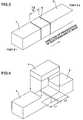
- Fig. 3shows an example of this arrangement.
- a state of a dielectric waveguide from which upper and lower dielectric plates are removedis illustrated in Fig. 3.
- the effect of interposing, between two dielectric strips 1 and 2 to be connected to each other, a dielectric strip 3 having a length corresponding to an odd number multiple of 1/4 of the guide wavelength of an electromagnetic wave propagating through the dielectric stripsis as described below.
- a wave reflected at the dielectric strip 1-3 connection plane and a wave reflected at the dielectric strip 2-3 connection planeare in phase opposition to each other. Therefore, these waves can cancel out and propagation of reflected waves to a port 1 or port 2 is limited.
- a third dielectric stripis partially inserted in a connection section of a first dielectric strip and a second dielectric strip to be connected to each other, and the distances between the three connection planes in said connection section are determined so that a wave reflected at the connection plane between the first and third dielectric strips, a wave reflected at the connection plane between the first and second dielectric strips, and a wave reflected at the connection plane between the second and third dielectric strips are superposed with a phase difference of 2 ⁇ /3 from each other.
- the phase of a reflected wave at the first-third dielectric strip connection planeis 0; the phase of a reflected wave at the first-second dielectric strip connection plane is 2 ⁇ /3 (120°); and the phase of a reflected wave at the second-third dielectric strip connection plane is 4 ⁇ /3 (240°), and if the reflected waves are equal in intensity, each of the real and imaginary part of the resultant wave is zero. Thus, the three reflected waves cancel out.
- the distance between the first-second dielectric connection plane and the first-third dielectric strip connection planeis set to 1/6 of the guide wavelength of an electromagnetic wave propagating through the dielectric strips, and the distance between the first-second dielectric strip connection plane and the second-third dielectric strip connection plane is set to 1/6 of the guide wavelength.
- Fig. 4shows the configuration of an example of this dielectric waveguide. In Fig. 4, conductor plates located above and below dielectric strips are omitted.
- Waves reflected at the connection planescan be canceled out by partially inserting a third dielectric strip in a connection section of a first dielectric strip 1 and a second dielectric strip 2 and by setting each of the distances L1 and L2 between the two connection planes to ⁇ g/6.
- the pair of dielectric waveguidesare positioned along a direction parallel to the conductor plates and along a direction perpendicular to the electromagnetic wave propagation direction by projecting a portion of one of the conductor plates in the opposed surfaces of the conductor plates at the connection between the pair of dielectric waveguides while recessing the corresponding opposite conductor plate at a corresponding position.
- Fig. 5is a cross-sectional view of an essential portion of the dielectric waveguide.
- grooves each having a depth gare respectively formed in conductor plates 4 and 5
- dielectric stripsare respectively set in the grooves, and the conductor plates 4 and 5 with the dielectric strips are positioned relative to each other so that the dielectric strips are opposed to each other.
- Fig. 6is a perspective view of the construction of the dielectric strips shown without the upper and lower conductor plates.
- members 1a and 2acorrespond to the dielectric strip provided on the lower conductor plate 4 shown in Fig. 5
- members 1b and 2bcorrespond to the dielectric strip provided on the upper conductor plate shown in Fig. 5.
- the distance L between dielectric strip 1a-2a connection plane a and dielectric strip 1b-2b connection plane bis set to ⁇ g/4.
- dielectric strips 1 and 2each formed of one integral body as shown in Fig. 8A may alternatively be used.
- a structure such as shown in Fig. 8Bmay be used, in which one dielectric strip 1 is formed of one integral body while a pair of half dielectric strips 2a and 2b are provided on the other side. The same effect of the present invention can also be obtained by using such a structure.
- Fig. 9is a perspective view of the construction of dielectric strips shown without upper and lower conductor plates.
- each of the dielectric strip 1a-2a connection plane a and the dielectric strip 1b-2b connection plane bis perpendicular to each of the upper and lower conductor plates.
- dielectric strips 1 and 2 each formed of one integral bodymay alternatively be used as shown in Fig. 11 to obtain the same effect.
- the dielectric stripscan be manufactured by punching, which is advantageous in mass-producibility and in cost reduction effect.
- connection planesare set perpendicular to the direction of propagation of electromagnetic waves.
- the connection planesmay be set obliquely while being maintained parallel to each other, with the distance L between the two connection planes in the direction of propagation of electromagnetic waves set to ⁇ g/4.
- the configuration of a dielectric waveguide which represents a third embodiment of the present inventionwill next be described below with reference to Figs. 13 to 15.
- the third embodimentis arranged in such a manner that a dielectric plate is interposed between two conductor plates, and a planar circuit is formed on the dielectric plate.
- Fig. 13is a cross-sectional view of the structure of this waveguide.
- Grooves each having a depth gare respectively formed in conductor plates 4 and 5
- dielectric strips 1a and 1bare respectively set in the grooves, and a dielectric plate 6 is interposed between the two dielectric strips.
- conductor patterns for a microstrip line, a coplanar line, a slot lines or the likeare formed and electronic components including a semiconductor element or the like are mounted.
- Fig. 14is a perspective view of this structure shown without the upper and lower conductor plates.
- the distance L between the dielectric strip 1a-2a connection plane defined on the lower side of the dielectric plate 6 as viewed in Fig. 14 and the dielectric strip 1b-2b connection plane defined on the upper side of the dielectric plate 6is set to an odd number multiple of ⁇ g/4. Also in this case, a reflection characteristic in the operating band as favorable as those in the first and second embodiments can be obtained.
- connection planessuch as those shown in Fig. 14 perpendicular to the direction of propagation of electromagnetic waves.
- the dielectric stripsmay have connection planes inclined at a predetermined angle from a plane perpendicular to the direction of propagation of electromagnetic waves, as shown in Fig. 15A or 15B. (In Figs. 15A and 15B, the dielectric plate between the upper and lower dielectric strips is omitted.) Also in such a case, the arrangement may be such that the distance L between the two connection planes in the direction of propagation of electromagnetic waves corresponds to an odd number multiple of ⁇ g/4 while the two connection planes are set substantially parallel to each other.
- Fig. 16Ais a perspective view of dielectric strips shown without upper and lower conductor plates, and shows the connection structure of the dielectric strips.
- Fig. 16Bis an exploded perspective view of the dielectric strips. While the dielectric strips are connected to each other at two connection planes in each of the above-described embodiments, the dielectric strips in this embodiment are connected at three connection planes a, b, and c perpendicular to the direction of propagation of electromagnetic waves. The distance L between the connection planes is set to an odd number multiple of ⁇ g/4.
- Fig. 17Ais a perspective view of dielectric strips shown without upper and lower conductor plates, and shows the connection structure of the dielectric strips.
- Fig. 17Bis an exploded perspective view of the dielectric strips.
- the dielectric stripsare connected at four connection planes a, b, c, and d.
- propagation of reflected waves to a port #1 or a port #2can be limited by setting the distance L between the connection planes to an odd number multiple of ⁇ g/4.
- Figs. 18 and 19are perspective views of waveguides shown without upper and lower conductor plates.
- the dielectric constants of the dielectric strips 1, 2a, and 2b, and the dielectric plate 6are set approximately equal to each other, or the dielectric constant of the dielectric plate 6 is set slightly smaller than the dielectric constants of the dielectric strips 1, 2a, and 2b, so that the line impedances of the portion in which the dielectric plate 6 is inserted and the portion in which the dielectric plate 6 is not inserted are approximately equal to each other.
- a recessis provided in the dielectric plate 6 as shown in Fig. 19 to set the line impedance at the recess to a middle value between the line impedance of the portion in which the dielectric plate is inserted and the line impedance of the portion in which the dielectric plate is not inserted.
- Fig. 20is a perspective view in a state where upper and lower conductor plates are removed.
- This dielectric waveguidediffers from that illustrated in Fig. 18 in that four dielectric strips 1a, 1b, 2a, and 2b are used. Also in this case, the distance L between the connection plane a and the connection plane b is set to an odd number multiple of ⁇ g/4.
- Figs. 21 and 22are cross-sectional views of dielectric strip portions along the direction of propagation of electromagnetic waves.
- the thicknesses of the dielectric strips 1b and 2bare equal to each other while the thickness of the dielectric strip 1a is equal to the sum of the thickness of the dielectric strip 2a and the thickness of the dielectric plate 6.
- the thickness of the entire dielectric strip 1bis equal to that of the dielectric strip 1a
- the thicknesses of the dielectric strips 2a and 2bare equal to each other
- the height of the connection plane between the dielectric strips 1a and 1bcorresponds to the center of the end surface of the dielectric plate 6 in the direction of height.
- the structure shown in Fig. 22is symmetrical about a horizontal plane, so that the facility with which the dielectric waveguide is designed is improved.
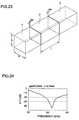
- Fig. 23is a diagram showing the configuration of a dielectric waveguide which represents a seventh embodiment of the present invention.
- a dielectric strip 3having a length corresponding to an odd number multiple of ⁇ g/4 is interposed between two dielectric strips 1 and 2 which are to be connected to each other.
- a wave reflected at the dielectric strip 1-3 connection plane and a wave reflected at the dielectric strip 2-3 connection planeare superposed in phase opposition to each other to be canceled out. In this manner, reflected waves propagating to a port 1 and to a port 2 are reduced.
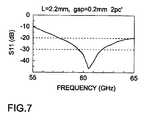
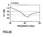
- Fig. 24shows the result of calculation of a reflection characteristic in the 60 GHz band of the dielectric waveguide shown in Fig. 23.
- a2.2 mm
- b1.8 mm
- d0.5 mm (see Fig. 1)
- gap0.2 mm
- L2.2 mm
- LL10 mm
- ⁇ r2.04.
- each dielectric strip in the structure shown in Fig. 23can be worked by being cut along a plane perpendicular to its axial direction.
- the facility with which the dielectric waveguide is manufacturedcan be improved.
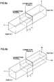
- Figs. 25A and 25Bare diagrams showing a dielectric waveguide which represents an eighth embodiment of the present invention.
- Fig. 25Ais a perspective view of dielectric strips shown without upper and lower conductor plates
- Fig. 25Bis an exploded perspective view of the dielectric strips.
- a third dielectric strip 3is inserted in a connection section of first and second dielectric strips 1 and 2, and each of the distances L1 and L2 between two pairs of connection planes is set to ⁇ g/6, thereby enabling waves reflected at the connection planes to cancel out.
- Fig. 26shows the result of calculation of a reflection characteristic in the 60 GHz band of the dielectric waveguide shown in Fig. 25.
- the guide wavelength ⁇ g at 60 GHzis 8.7 mm. It can be understood from this result that an improved reflection characteristic at the operating frequency (60 GHz band) can be obtained even in the case where there are three connection planes.
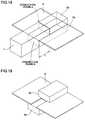
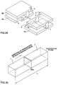
- Figs. 27 and 28are exploded perspective views of a dielectric waveguide device which represents a ninth embodiment of the present invention.
- each of components of a mixer or an oscillatoris separately manufactured and the prepared components are combined to form a dielectric waveguide device.
- Fig. 27Ais a diagram showing a state of two components 20 and 21 before assembly
- Fig. 27Bis a perspective view of the connection structure of dielectric strip portions used in the two components 20 and 21.
- the component 20has conductor plates 4a and 5a and has dielectric strips 1a and 1b provided between the conductor plates 4a and 5b, as shown in Fig. 27B.
- the component 21has dielectric strips 2a and 2b provided between conductor plates 4b and 5b.
- a planar circuit on a dielectric plateis formed inside these components 20 and 21 according to one's need.
- the end surface of the conductor plate 5aprotrudes by L beyond the end surface of the conductor plate 4a.
- the end surface of the conductor plate 4bprotrudes by L beyond the end surface of the conductor plate 5b.
- the distance between the dielectric strip 1b-2b connection plane a and the dielectric strip 1a-2a connection plane bis set to L, as shown in Fig. 27B.
- these two components 20 and 21are positioned relative to each other along the vertical direction as viewed in the figure by abutment of the lower surface of the protruding portion of the conductor plate 5a and the upper surface of the protruding portion of the conductor plate 4b and by abutment of the upper surface of the protruding portion of the dielectric strip 2a and the lower surface of the protruding portion of the dielectric strip 1b.
- the two components 20 and 21are also positioned along the electromagnetic wave propagation direction by abutment of the end surfaces of the dielectric plates 4a and 5a, and 4b and 5b, and by abutment of the end surfaces of the dielectric strips 1a and 1b, and 2a and 2b.
- Fig. 28shows an example of positioning in a dielectric waveguide along a direction perpendicular to the electromagnetic wave propagation direction and along a horizontal direction as viewed in the figure.
- Positioning pins 7 and 8are provided on the conductor plate 4b, and positioning holes 9 and 10 are formed in corresponding positions in the conductor plate 5a.
- the components 21 and 22are positioned by fitting the positioning pins 7 and 8 projecting from the component 21 to the positioning holes 9 and 10 of the component 20.
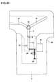
- Fig. 29is an exploded perspective view of an oscillator with which an isolator is integrally combined, and which represents a tenth embodiment of the present invention
- Fig. 30is a plan view of components in a superposed state.
- Components 2, 31, and 32 shown in Figs. 29 and 30are dielectric strips, and a component 34 is a ferrite disk. These components are disposed between a conductor plate 35 and another conductor plate (not shown) opposed to each other.
- a resistor 33is provided at a terminal of the dielectric strip 32. Further, a magnet for applying a dc magnetic field to the ferrite disk 34 is provided. These components form an isolator.
- An end portion of the dielectric strip 2is formed so as to have a step portion.
- a dielectric strip 1ais placed on the conductor plate 35 continuously with the step portion of the dielectric strip 2.
- a dielectric plate 6is placed on the end step portion of the dielectric strip 2, on the dielectric strip 1a and on a portion of the conductor plate 36.
- the dielectric plate 6has a cut portion S at its one end.
- the cut portion Scorresponds to the step portion of the dielectric strip 2.
- a dielectric strip 1bis placed at a position on the dielectric plate 6 opposite from the dielectric strip 1a, thus forming a structure in which the dielectric plate 6 is interposed between the upper and lower dielectric strips. This structure enables impedance matching by setting the impedance of the line at the step portion of the dielectric strip 2 as a middle value between the impedance of the line at the dielectric strip 1a and the impedance of the line at the dielectric strip 2.
- the length of the dielectric strip 1bis approximately equal to the sum of the dielectric strip 1a and the length of the step portion of the dielectric strip 2.
- the length of the step portion at the end of the dielectric strip 2is set an odd number multiple of 1/4 of the guide wavelength of an electromagnetic wave propagating through the dielectric strips. Waves reflected at the two connection planes between the dielectric strip 2 and the dielectric strips 1a and 1b are thereby made to cancel out.
- an excitation probe 38On the dielectric plate 6, an excitation probe 38, a low-pass filter 39, and a bias electrodes 40 are formed.
- a Gunn diode block 36is provided on the conductor plate 35, and a Gunn diode is connected to the excitation probe 38 on the dielectric plate 6, and the excitation probe 38 is positioned at the ends of the dielectric strips 1a and 1b.
- a dielectric resonator 37is also provided on the dielectric plate 6. The dielectric resonator 37 is disposed close to the dielectric strips 1a and 1b to couple with the same.
- a bias voltageis applied to the bias electrode 40 to supply a bias voltage to the Gunn diode.
- the Gunn diodethereby oscillates a signal, which propagates through the dielectric strips 1a and 1b, the dielectric strips 1a and 1b and the nonradiative dielectric waveguide formed of the dielectric strips 1a and 1b and the upper and lower conductor plates via the excitation probe 38.
- This signalpropagates in the direction from the dielectric strip 2 toward the dielectric strip 31.
- the dielectric resonator 37stabilizes the oscillation frequency of the Gunn diode.
- the low-pass filter 39suppresses a leak of a high-frequency signal to the bias electrode 40.
- a reflected wave from the dielectric strip 31is guided in the direction toward the dielectric strip 32 by the operation of the isolator and is terminated by the resistor 33 in a non-reflection manner. Therefore, no reflected wave returns from the dielectric strip 31 to the Gunn diode. Also, waves reflected at the two connection planes between the dielectric strips 1a and 1b and the dielectric strip 2 cancel out and do not return to the Gunn diode. Thus, an oscillator having stabilized characteristics can be obtained.
- Fig. 32shows another example of the connection structure of dielectric waveguides.
- one dielectric waveguidehas grooves formed in conductor plates 4a and 5a, and has a dielectric strip 1 fit to the grooves.
- Another dielectric waveguidehas grooves formed in conductor plates 4b and 5b, and has a dielectric strip 2 fit to the grooves. Portions of the dielectric strips 1 and 2 opposed to each other are stepped so that the distance between the two connection planes is 1/4 of the guide wavelength.
- the opposed surfaces of the dielectric plates at the connection between the two dielectric waveguidesare formed in such a manner that, as shown in Fig. 32, a portion p of one conductor plate 5a projects while the other conductor plate 5b opposed to the conductor plate 5a is recessed at the corresponding position d, thus forming step portions s.
- This structureenables the two dielectric waveguides to be positioned relative to each other along a direction parallel to the flat surfaces of the conductor plates and along a direction perpendicular to the electromagnetic wave propagation direction (the longitudinal direction of the dielectric strips) by abutment of the side surfaces of the above-described step portions when they are opposed to each other with a certain gap formed therebetween, or when they are brought into abutment on each other.
- Fig. 33shows still another example of the connection structure of dielectric waveguides.
- This examplediffers from that shown in Fig. 32 in that, in the opposed end surfaces of the pairs of conductor plates at the connection between two dielectric waveguides, a portions p of each of the conductor plates 4a and 5a on one side projects while the conductor plates 4b and 5b on the other side are recessed at corresponding positions d, thereby forming step portions s.
- This structureenables the two dielectric waveguides to be positioned relative to each other along a direction parallel to the flat surfaces of the conductor plates and along a direction perpendicular to the electromagnetic wave propagation direction by abutment of the side surfaces of the above-described step portions when they are opposed to each other with a certain gap formed therebetween, or when they are brought into abutment on each other.
- step portionsare formed in only one place as viewed in plan.
- the arrangementmay alternatively be such that, for example, as shown in Fig. 34, step portions s are formed in two places so that their side surfaces face in different directions, thereby enabling positioning along each of a direction parallel to the flat surfaces of the conductor plates and a direction perpendicular to the electromagnetic wave propagation direction.
- the embodimentshave been described with respect to the grooved type dielectric waveguides in which the distance between the flat surfaces of the portions of the conductor plates at the dielectric strip portions is increased relative to the distance between the flat conductor surfaces in the other regions.
- the present inventioncan also be applied in the same manner to a normal type dielectric waveguide such as shown in Fig. 31A.
- conductor plates each formed of a metal plate or the likeare used as flat conductors between which dielectric strip portions are interposed, and dielectric strips are provided separately from the conductor portions having flat surfaces.
- the present inventioncan also be applied in the same manner to, for example, a window type dielectric waveguide constructed in such a manner that, as shown in Fig. 31B, dielectric strip portions are integrally formed on dielectric plates 11 and 12, electrodes 13 and 14 are provided on external surfaces of the dielectric plates, and the dielectric strip portions are opposed to each other.
- electromagnetic waves reflected at the connection planesare superposed to cancel out, thereby reducing the influence of reflection. Therefore, a dielectric waveguide having an improved reflection characteristic can be obtained even if the difference between the linear expansion coefficients of dielectric strips and conductor plates is large, even if the waveguide is used in an environment where there are large variations in temperature, or even if a comparatively large gap is formed between the surfaces of the dielectric strips connected to each other due to a large working tolerance.
- two dielectric waveguidescan be positioned along a direction parallel to the conductor plates and along a direction perpendicular to the electromagnetic wave propagation direction. Therefore, a dielectric waveguide can be obtained in which reflection at a connection plane between two dielectric waveguides can be limited and which has an improved transmission line characteristic
Landscapes
- Waveguides (AREA)
- Waveguide Connection Structure (AREA)
- Radar Systems Or Details Thereof (AREA)
- Waveguide Aerials (AREA)
Abstract
Description
Claims (6)
- A dielectric waveguide comprising:an electromagnetic wave propagation region formed bydisposing a plurality of dielectric strips (1, 2) along adirection of propagation of an electromagnetic wave,
wherein adjacent pairs of dielectric strips (1, 2) areconnected at a plurality of planes spaced apart from eachother in the direction of propagation of an electromagneticwave by a distance corresponding to an odd number multipleof 1/4 of the guide wavelength of the electromagnetic wavepropagating through the dielectric strips. - A dielectric waveguide comprising:an electromagnetic wave propagation region formed bydisposing a plurality of dielectric strip portions (1, 2, 3)along a direction of propagation of an electromagnetic wave,
wherein, between two dielectric strips (1, 2) to beconnected to each other, another dielectric strip (3) havinga length corresponding to an odd number multiple of 1/4 ofthe guide wavelength of an electromagnetic wave propagatingthrough the dielectric strips (1, 2) is interposed. - A dielectric waveguide comprising:an electromagnetic wave propagation region formed bydisposing a plurality of dielectric strip portions (1, 2, 3) along a direction of propagation of an electromagnetic wave,
wherein a third dielectric strip (3) is partiallyinserted in a connection section of a first dielectric strip(1) and a second dielectric strip (2) to be connected toeach other, and the distances between the three connectionplanes in said connection section are determined so that awave reflected at the connection plane between the first andthird dielectric strips (1, 3), a wave reflected at theconnection plane between the first and second dielectricstrips (1, 2), and a wave reflected at the connection planebetween the second and third dielectric strips (2, 3) aresuperposed with a phase difference of 2π/3 from each other. - A dielectric waveguide according to Claim 3,wherein the distance between the first-second dielectricstrip connection plane (b) and the first-third dielectricstrip connection plane (c) is set to 1/6 of the guidewavelength of an electromagnetic wave propagating throughthe dielectric strips, and the distance between the first-seconddielectric strip connection plane (b) and the second-thirddielectric strip connection plane (a) is set to 1/6 ofthe guide wavelength.
- A dielectric resonator according to any one ofClaims 1 to 4, wherein said dielectric waveguide is formed of two conductor plates (4a, 5a, 4b, 5b) and a dielectricstrip (1, 2) placed between the two conductor plates and apair of said dielectric waveguides are positioned along adirection parallel to said conductor plates and along adirection perpendicular to the electromagnetic wavepropagation direction by projecting a portion (p) of one ofthe conductor plates in the opposed surfaces of theconductor plates at the connection between the pair of saiddielectric waveguides while recessing the correspondingopposite conductor plate at a corresponding position (d).
- A dielectric resonator comprising:a plurality of dielectric waveguides each having adielectric strip (1) placed between two conductor plates (4,5),
wherein a pair of said dielectric waveguides arepositioned along a direction parallel to said conductorplates (4, 5) and along a direction perpendicular to theelectromagnetic wave propagation direction by projecting aportion (p) of one of the conductor plates in the opposedsurfaces of the conductor plates at the connection betweenthe pair of said dielectric waveguides while recessing thecorresponding opposite conductor plate at a correspondingposition (d).
Priority Applications (1)
| Application Number | Priority Date | Filing Date | Title |
|---|---|---|---|
| EP04016766AEP1473796B1 (en) | 1997-07-11 | 1998-06-30 | Dielectric waveguide |
Applications Claiming Priority (6)
| Application Number | Priority Date | Filing Date | Title |
|---|---|---|---|
| JP18635897 | 1997-07-11 | ||
| JP186358/97 | 1997-07-11 | ||
| JP18635897 | 1997-07-11 | ||
| JP3620498 | 1998-02-18 | ||
| JP36204/98 | 1998-02-18 | ||
| JP03620498AJP3269448B2 (en) | 1997-07-11 | 1998-02-18 | Dielectric line |
Related Child Applications (1)
| Application Number | Title | Priority Date | Filing Date |
|---|---|---|---|
| EP04016766ADivisionEP1473796B1 (en) | 1997-07-11 | 1998-06-30 | Dielectric waveguide |
Publications (3)
| Publication Number | Publication Date |
|---|---|
| EP0896380A2true EP0896380A2 (en) | 1999-02-10 |
| EP0896380A3 EP0896380A3 (en) | 2000-07-12 |
| EP0896380B1 EP0896380B1 (en) | 2008-01-02 |
Family
ID=26375247
Family Applications (2)
| Application Number | Title | Priority Date | Filing Date |
|---|---|---|---|
| EP98112065AExpired - LifetimeEP0896380B1 (en) | 1997-07-11 | 1998-06-30 | Dielectric waveguide |
| EP04016766AExpired - LifetimeEP1473796B1 (en) | 1997-07-11 | 1998-06-30 | Dielectric waveguide |
Family Applications After (1)
| Application Number | Title | Priority Date | Filing Date |
|---|---|---|---|
| EP04016766AExpired - LifetimeEP1473796B1 (en) | 1997-07-11 | 1998-06-30 | Dielectric waveguide |
Country Status (4)
| Country | Link |
|---|---|
| US (2) | US6307451B1 (en) |
| EP (2) | EP0896380B1 (en) |
| JP (1) | JP3269448B2 (en) |
| DE (2) | DE69838932T2 (en) |
Cited By (171)
| Publication number | Priority date | Publication date | Assignee | Title |
|---|---|---|---|---|
| EP1130680A3 (en)* | 2000-02-29 | 2002-08-07 | Anritsu Corporation | Dielectric leaky-wave antenna |
| WO2014026089A1 (en)* | 2012-08-10 | 2014-02-13 | Waveconnex, Inc. | Dielectric coupling systems for ehf communications |
| US9197011B2 (en) | 2011-12-14 | 2015-11-24 | Keyssa, Inc. | Connectors providing haptic feedback |
| US9203597B2 (en) | 2012-03-02 | 2015-12-01 | Keyssa, Inc. | Systems and methods for duplex communication |
| US9322904B2 (en) | 2011-06-15 | 2016-04-26 | Keyssa, Inc. | Proximity sensing using EHF signals |
| US9374154B2 (en) | 2012-09-14 | 2016-06-21 | Keyssa, Inc. | Wireless connections with virtual hysteresis |
| US9379450B2 (en) | 2011-03-24 | 2016-06-28 | Keyssa, Inc. | Integrated circuit with electromagnetic communication |
| US9407311B2 (en) | 2011-10-21 | 2016-08-02 | Keyssa, Inc. | Contactless signal splicing using an extremely high frequency (EHF) communication link |
| US9426660B2 (en) | 2013-03-15 | 2016-08-23 | Keyssa, Inc. | EHF secure communication device |
| WO2016182667A1 (en)* | 2015-05-14 | 2016-11-17 | At&T Intellectual Property I, Lp | Waveguide having a nonconductive material and methods for use therewith |
| US9515859B2 (en) | 2011-05-31 | 2016-12-06 | Keyssa, Inc. | Delta modulated low-power EHF communication link |
| US9531425B2 (en) | 2012-12-17 | 2016-12-27 | Keyssa, Inc. | Modular electronics |
| US9553353B2 (en) | 2012-03-28 | 2017-01-24 | Keyssa, Inc. | Redirection of electromagnetic signals using substrate structures |
| US9553616B2 (en) | 2013-03-15 | 2017-01-24 | Keyssa, Inc. | Extremely high frequency communication chip |
| US9608740B2 (en) | 2015-07-15 | 2017-03-28 | At&T Intellectual Property I, L.P. | Method and apparatus for launching a wave mode that mitigates interference |
| US9608692B2 (en) | 2015-06-11 | 2017-03-28 | At&T Intellectual Property I, L.P. | Repeater and methods for use therewith |
| US9615269B2 (en) | 2014-10-02 | 2017-04-04 | At&T Intellectual Property I, L.P. | Method and apparatus that provides fault tolerance in a communication network |
| US9628116B2 (en) | 2015-07-14 | 2017-04-18 | At&T Intellectual Property I, L.P. | Apparatus and methods for transmitting wireless signals |
| US9627768B2 (en) | 2014-10-21 | 2017-04-18 | At&T Intellectual Property I, L.P. | Guided-wave transmission device with non-fundamental mode propagation and methods for use therewith |
| US9628854B2 (en) | 2014-09-29 | 2017-04-18 | At&T Intellectual Property I, L.P. | Method and apparatus for distributing content in a communication network |
| US9640850B2 (en) | 2015-06-25 | 2017-05-02 | At&T Intellectual Property I, L.P. | Methods and apparatus for inducing a non-fundamental wave mode on a transmission medium |
| US9653770B2 (en) | 2014-10-21 | 2017-05-16 | At&T Intellectual Property I, L.P. | Guided wave coupler, coupling module and methods for use therewith |
| US9654173B2 (en) | 2014-11-20 | 2017-05-16 | At&T Intellectual Property I, L.P. | Apparatus for powering a communication device and methods thereof |
| US9661505B2 (en) | 2013-11-06 | 2017-05-23 | At&T Intellectual Property I, L.P. | Surface-wave communications and methods thereof |
| US9667317B2 (en) | 2015-06-15 | 2017-05-30 | At&T Intellectual Property I, L.P. | Method and apparatus for providing security using network traffic adjustments |
| US9680670B2 (en) | 2014-11-20 | 2017-06-13 | At&T Intellectual Property I, L.P. | Transmission device with channel equalization and control and methods for use therewith |
| US9685992B2 (en) | 2014-10-03 | 2017-06-20 | At&T Intellectual Property I, L.P. | Circuit panel network and methods thereof |
| US9692101B2 (en) | 2014-08-26 | 2017-06-27 | At&T Intellectual Property I, L.P. | Guided wave couplers for coupling electromagnetic waves between a waveguide surface and a surface of a wire |
| US9699785B2 (en) | 2012-12-05 | 2017-07-04 | At&T Intellectual Property I, L.P. | Backhaul link for distributed antenna system |
| US9705610B2 (en) | 2014-10-21 | 2017-07-11 | At&T Intellectual Property I, L.P. | Transmission device with impairment compensation and methods for use therewith |
| US9705571B2 (en) | 2015-09-16 | 2017-07-11 | At&T Intellectual Property I, L.P. | Method and apparatus for use with a radio distributed antenna system |
| US9722318B2 (en) | 2015-07-14 | 2017-08-01 | At&T Intellectual Property I, L.P. | Method and apparatus for coupling an antenna to a device |
| US9729197B2 (en) | 2015-10-01 | 2017-08-08 | At&T Intellectual Property I, L.P. | Method and apparatus for communicating network management traffic over a network |
| US9735833B2 (en) | 2015-07-31 | 2017-08-15 | At&T Intellectual Property I, L.P. | Method and apparatus for communications management in a neighborhood network |
| US9742521B2 (en) | 2014-11-20 | 2017-08-22 | At&T Intellectual Property I, L.P. | Transmission device with mode division multiplexing and methods for use therewith |
| US9742462B2 (en) | 2014-12-04 | 2017-08-22 | At&T Intellectual Property I, L.P. | Transmission medium and communication interfaces and methods for use therewith |
| US9762289B2 (en) | 2014-10-14 | 2017-09-12 | At&T Intellectual Property I, L.P. | Method and apparatus for transmitting or receiving signals in a transportation system |
| US9769128B2 (en) | 2015-09-28 | 2017-09-19 | At&T Intellectual Property I, L.P. | Method and apparatus for encryption of communications over a network |
| US9768833B2 (en) | 2014-09-15 | 2017-09-19 | At&T Intellectual Property I, L.P. | Method and apparatus for sensing a condition in a transmission medium of electromagnetic waves |
| US9769020B2 (en) | 2014-10-21 | 2017-09-19 | At&T Intellectual Property I, L.P. | Method and apparatus for responding to events affecting communications in a communication network |
| US9780834B2 (en) | 2014-10-21 | 2017-10-03 | At&T Intellectual Property I, L.P. | Method and apparatus for transmitting electromagnetic waves |
| US9787412B2 (en) | 2015-06-25 | 2017-10-10 | At&T Intellectual Property I, L.P. | Methods and apparatus for inducing a fundamental wave mode on a transmission medium |
| US9793955B2 (en) | 2015-04-24 | 2017-10-17 | At&T Intellectual Property I, Lp | Passive electrical coupling device and methods for use therewith |
| US9793951B2 (en) | 2015-07-15 | 2017-10-17 | At&T Intellectual Property I, L.P. | Method and apparatus for launching a wave mode that mitigates interference |
| US9794003B2 (en) | 2013-12-10 | 2017-10-17 | At&T Intellectual Property I, L.P. | Quasi-optical coupler |
| US9800327B2 (en) | 2014-11-20 | 2017-10-24 | At&T Intellectual Property I, L.P. | Apparatus for controlling operations of a communication device and methods thereof |
| US9806818B2 (en) | 2015-07-23 | 2017-10-31 | At&T Intellectual Property I, Lp | Node device, repeater and methods for use therewith |
| US9820146B2 (en) | 2015-06-12 | 2017-11-14 | At&T Intellectual Property I, L.P. | Method and apparatus for authentication and identity management of communicating devices |
| US9831912B2 (en) | 2015-04-24 | 2017-11-28 | At&T Intellectual Property I, Lp | Directional coupling device and methods for use therewith |
| US9836957B2 (en) | 2015-07-14 | 2017-12-05 | At&T Intellectual Property I, L.P. | Method and apparatus for communicating with premises equipment |
| US9838078B2 (en) | 2015-07-31 | 2017-12-05 | At&T Intellectual Property I, L.P. | Method and apparatus for exchanging communication signals |
| US9838896B1 (en) | 2016-12-09 | 2017-12-05 | At&T Intellectual Property I, L.P. | Method and apparatus for assessing network coverage |
| US9847850B2 (en) | 2014-10-14 | 2017-12-19 | At&T Intellectual Property I, L.P. | Method and apparatus for adjusting a mode of communication in a communication network |
| US9847566B2 (en) | 2015-07-14 | 2017-12-19 | At&T Intellectual Property I, L.P. | Method and apparatus for adjusting a field of a signal to mitigate interference |
| US9853696B2 (en) | 2008-12-23 | 2017-12-26 | Keyssa, Inc. | Tightly-coupled near-field communication-link connector-replacement chips |
| US9853342B2 (en) | 2015-07-14 | 2017-12-26 | At&T Intellectual Property I, L.P. | Dielectric transmission medium connector and methods for use therewith |
| US9860075B1 (en) | 2016-08-26 | 2018-01-02 | At&T Intellectual Property I, L.P. | Method and communication node for broadband distribution |
| US9866276B2 (en) | 2014-10-10 | 2018-01-09 | At&T Intellectual Property I, L.P. | Method and apparatus for arranging communication sessions in a communication system |
| US9865911B2 (en) | 2015-06-25 | 2018-01-09 | At&T Intellectual Property I, L.P. | Waveguide system for slot radiating first electromagnetic waves that are combined into a non-fundamental wave mode second electromagnetic wave on a transmission medium |
| US9866309B2 (en) | 2015-06-03 | 2018-01-09 | At&T Intellectual Property I, Lp | Host node device and methods for use therewith |
| US9871558B2 (en) | 2014-10-21 | 2018-01-16 | At&T Intellectual Property I, L.P. | Guided-wave transmission device and methods for use therewith |
| US9871283B2 (en) | 2015-07-23 | 2018-01-16 | At&T Intellectual Property I, Lp | Transmission medium having a dielectric core comprised of plural members connected by a ball and socket configuration |
| US9876570B2 (en) | 2015-02-20 | 2018-01-23 | At&T Intellectual Property I, Lp | Guided-wave transmission device with non-fundamental mode propagation and methods for use therewith |
| US9876605B1 (en) | 2016-10-21 | 2018-01-23 | At&T Intellectual Property I, L.P. | Launcher and coupling system to support desired guided wave mode |
| US9876264B2 (en) | 2015-10-02 | 2018-01-23 | At&T Intellectual Property I, Lp | Communication system, guided wave switch and methods for use therewith |
| US9882277B2 (en) | 2015-10-02 | 2018-01-30 | At&T Intellectual Property I, Lp | Communication device and antenna assembly with actuated gimbal mount |
| US9882257B2 (en) | 2015-07-14 | 2018-01-30 | At&T Intellectual Property I, L.P. | Method and apparatus for launching a wave mode that mitigates interference |
| US9887447B2 (en) | 2015-05-14 | 2018-02-06 | At&T Intellectual Property I, L.P. | Transmission medium having multiple cores and methods for use therewith |
| US9893795B1 (en) | 2016-12-07 | 2018-02-13 | At&T Intellectual Property I, Lp | Method and repeater for broadband distribution |
| US9904535B2 (en) | 2015-09-14 | 2018-02-27 | At&T Intellectual Property I, L.P. | Method and apparatus for distributing software |
| US9906269B2 (en) | 2014-09-17 | 2018-02-27 | At&T Intellectual Property I, L.P. | Monitoring and mitigating conditions in a communication network |
| US9912027B2 (en) | 2015-07-23 | 2018-03-06 | At&T Intellectual Property I, L.P. | Method and apparatus for exchanging communication signals |
| US9912419B1 (en) | 2016-08-24 | 2018-03-06 | At&T Intellectual Property I, L.P. | Method and apparatus for managing a fault in a distributed antenna system |
| US9913139B2 (en) | 2015-06-09 | 2018-03-06 | At&T Intellectual Property I, L.P. | Signal fingerprinting for authentication of communicating devices |
| US9912382B2 (en) | 2015-06-03 | 2018-03-06 | At&T Intellectual Property I, Lp | Network termination and methods for use therewith |
| US9911020B1 (en) | 2016-12-08 | 2018-03-06 | At&T Intellectual Property I, L.P. | Method and apparatus for tracking via a radio frequency identification device |
| US9917341B2 (en) | 2015-05-27 | 2018-03-13 | At&T Intellectual Property I, L.P. | Apparatus and method for launching electromagnetic waves and for modifying radial dimensions of the propagating electromagnetic waves |
| US9930668B2 (en) | 2013-05-31 | 2018-03-27 | At&T Intellectual Property I, L.P. | Remote distributed antenna system |
| US9927517B1 (en) | 2016-12-06 | 2018-03-27 | At&T Intellectual Property I, L.P. | Apparatus and methods for sensing rainfall |
| US9948355B2 (en) | 2014-10-21 | 2018-04-17 | At&T Intellectual Property I, L.P. | Apparatus for providing communication services and methods thereof |
| US9948333B2 (en) | 2015-07-23 | 2018-04-17 | At&T Intellectual Property I, L.P. | Method and apparatus for wireless communications to mitigate interference |
| US9948354B2 (en) | 2015-04-28 | 2018-04-17 | At&T Intellectual Property I, L.P. | Magnetic coupling device with reflective plate and methods for use therewith |
| US9954287B2 (en) | 2014-11-20 | 2018-04-24 | At&T Intellectual Property I, L.P. | Apparatus for converting wireless signals and electromagnetic waves and methods thereof |
| US9967173B2 (en) | 2015-07-31 | 2018-05-08 | At&T Intellectual Property I, L.P. | Method and apparatus for authentication and identity management of communicating devices |
| US9973940B1 (en) | 2017-02-27 | 2018-05-15 | At&T Intellectual Property I, L.P. | Apparatus and methods for dynamic impedance matching of a guided wave launcher |
| US9991580B2 (en) | 2016-10-21 | 2018-06-05 | At&T Intellectual Property I, L.P. | Launcher and coupling system for guided wave mode cancellation |
| US9998870B1 (en) | 2016-12-08 | 2018-06-12 | At&T Intellectual Property I, L.P. | Method and apparatus for proximity sensing |
| US9997819B2 (en) | 2015-06-09 | 2018-06-12 | At&T Intellectual Property I, L.P. | Transmission medium and method for facilitating propagation of electromagnetic waves via a core |
| US9999038B2 (en) | 2013-05-31 | 2018-06-12 | At&T Intellectual Property I, L.P. | Remote distributed antenna system |
| US10009067B2 (en) | 2014-12-04 | 2018-06-26 | At&T Intellectual Property I, L.P. | Method and apparatus for configuring a communication interface |
| US10009065B2 (en) | 2012-12-05 | 2018-06-26 | At&T Intellectual Property I, L.P. | Backhaul link for distributed antenna system |
| US10009901B2 (en) | 2015-09-16 | 2018-06-26 | At&T Intellectual Property I, L.P. | Method, apparatus, and computer-readable storage medium for managing utilization of wireless resources between base stations |
| US10009063B2 (en) | 2015-09-16 | 2018-06-26 | At&T Intellectual Property I, L.P. | Method and apparatus for use with a radio distributed antenna system having an out-of-band reference signal |
| US10020587B2 (en) | 2015-07-31 | 2018-07-10 | At&T Intellectual Property I, L.P. | Radial antenna and methods for use therewith |
| US10020844B2 (en) | 2016-12-06 | 2018-07-10 | T&T Intellectual Property I, L.P. | Method and apparatus for broadcast communication via guided waves |
| US10027397B2 (en) | 2016-12-07 | 2018-07-17 | At&T Intellectual Property I, L.P. | Distributed antenna system and methods for use therewith |
| US10033107B2 (en) | 2015-07-14 | 2018-07-24 | At&T Intellectual Property I, L.P. | Method and apparatus for coupling an antenna to a device |
| US10033108B2 (en) | 2015-07-14 | 2018-07-24 | At&T Intellectual Property I, L.P. | Apparatus and methods for generating an electromagnetic wave having a wave mode that mitigates interference |
| US10044409B2 (en) | 2015-07-14 | 2018-08-07 | At&T Intellectual Property I, L.P. | Transmission medium and methods for use therewith |
| US10051629B2 (en) | 2015-09-16 | 2018-08-14 | At&T Intellectual Property I, L.P. | Method and apparatus for use with a radio distributed antenna system having an in-band reference signal |
| US10051483B2 (en) | 2015-10-16 | 2018-08-14 | At&T Intellectual Property I, L.P. | Method and apparatus for directing wireless signals |
| US10069535B2 (en) | 2016-12-08 | 2018-09-04 | At&T Intellectual Property I, L.P. | Apparatus and methods for launching electromagnetic waves having a certain electric field structure |
| US10074890B2 (en) | 2015-10-02 | 2018-09-11 | At&T Intellectual Property I, L.P. | Communication device and antenna with integrated light assembly |
| US10079661B2 (en) | 2015-09-16 | 2018-09-18 | At&T Intellectual Property I, L.P. | Method and apparatus for use with a radio distributed antenna system having a clock reference |
| US10090606B2 (en) | 2015-07-15 | 2018-10-02 | At&T Intellectual Property I, L.P. | Antenna system with dielectric array and methods for use therewith |
| US10090594B2 (en) | 2016-11-23 | 2018-10-02 | At&T Intellectual Property I, L.P. | Antenna system having structural configurations for assembly |
| US10103801B2 (en) | 2015-06-03 | 2018-10-16 | At&T Intellectual Property I, L.P. | Host node device and methods for use therewith |
| US10103422B2 (en) | 2016-12-08 | 2018-10-16 | At&T Intellectual Property I, L.P. | Method and apparatus for mounting network devices |
| US10135147B2 (en) | 2016-10-18 | 2018-11-20 | At&T Intellectual Property I, L.P. | Apparatus and methods for launching guided waves via an antenna |
| US10135146B2 (en) | 2016-10-18 | 2018-11-20 | At&T Intellectual Property I, L.P. | Apparatus and methods for launching guided waves via circuits |
| US10136434B2 (en) | 2015-09-16 | 2018-11-20 | At&T Intellectual Property I, L.P. | Method and apparatus for use with a radio distributed antenna system having an ultra-wideband control channel |
| US10135145B2 (en) | 2016-12-06 | 2018-11-20 | At&T Intellectual Property I, L.P. | Apparatus and methods for generating an electromagnetic wave along a transmission medium |
| US10142086B2 (en) | 2015-06-11 | 2018-11-27 | At&T Intellectual Property I, L.P. | Repeater and methods for use therewith |
| US10139820B2 (en) | 2016-12-07 | 2018-11-27 | At&T Intellectual Property I, L.P. | Method and apparatus for deploying equipment of a communication system |
| US10144036B2 (en) | 2015-01-30 | 2018-12-04 | At&T Intellectual Property I, L.P. | Method and apparatus for mitigating interference affecting a propagation of electromagnetic waves guided by a transmission medium |
| US10148016B2 (en) | 2015-07-14 | 2018-12-04 | At&T Intellectual Property I, L.P. | Apparatus and methods for communicating utilizing an antenna array |
| US10154493B2 (en) | 2015-06-03 | 2018-12-11 | At&T Intellectual Property I, L.P. | Network termination and methods for use therewith |
| US10168695B2 (en) | 2016-12-07 | 2019-01-01 | At&T Intellectual Property I, L.P. | Method and apparatus for controlling an unmanned aircraft |
| US10178445B2 (en) | 2016-11-23 | 2019-01-08 | At&T Intellectual Property I, L.P. | Methods, devices, and systems for load balancing between a plurality of waveguides |
| US10205655B2 (en) | 2015-07-14 | 2019-02-12 | At&T Intellectual Property I, L.P. | Apparatus and methods for communicating utilizing an antenna array and multiple communication paths |
| US10224634B2 (en) | 2016-11-03 | 2019-03-05 | At&T Intellectual Property I, L.P. | Methods and apparatus for adjusting an operational characteristic of an antenna |
| US10225025B2 (en) | 2016-11-03 | 2019-03-05 | At&T Intellectual Property I, L.P. | Method and apparatus for detecting a fault in a communication system |
| US10243270B2 (en) | 2016-12-07 | 2019-03-26 | At&T Intellectual Property I, L.P. | Beam adaptive multi-feed dielectric antenna system and methods for use therewith |
| US10243784B2 (en) | 2014-11-20 | 2019-03-26 | At&T Intellectual Property I, L.P. | System for generating topology information and methods thereof |
| US10264586B2 (en) | 2016-12-09 | 2019-04-16 | At&T Mobility Ii Llc | Cloud-based packet controller and methods for use therewith |
| US10291311B2 (en) | 2016-09-09 | 2019-05-14 | At&T Intellectual Property I, L.P. | Method and apparatus for mitigating a fault in a distributed antenna system |
| US10291334B2 (en) | 2016-11-03 | 2019-05-14 | At&T Intellectual Property I, L.P. | System for detecting a fault in a communication system |
| US10298293B2 (en) | 2017-03-13 | 2019-05-21 | At&T Intellectual Property I, L.P. | Apparatus of communication utilizing wireless network devices |
| US10305196B2 (en) | 2012-04-17 | 2019-05-28 | Keyssa, Inc. | Dielectric lens structures for EHF radiation |
| US10305190B2 (en) | 2016-12-01 | 2019-05-28 | At&T Intellectual Property I, L.P. | Reflecting dielectric antenna system and methods for use therewith |
| US10312567B2 (en) | 2016-10-26 | 2019-06-04 | At&T Intellectual Property I, L.P. | Launcher with planar strip antenna and methods for use therewith |
| US10320586B2 (en) | 2015-07-14 | 2019-06-11 | At&T Intellectual Property I, L.P. | Apparatus and methods for generating non-interfering electromagnetic waves on an insulated transmission medium |
| US10326494B2 (en) | 2016-12-06 | 2019-06-18 | At&T Intellectual Property I, L.P. | Apparatus for measurement de-embedding and methods for use therewith |
| US10326689B2 (en) | 2016-12-08 | 2019-06-18 | At&T Intellectual Property I, L.P. | Method and system for providing alternative communication paths |
| US10340573B2 (en) | 2016-10-26 | 2019-07-02 | At&T Intellectual Property I, L.P. | Launcher with cylindrical coupling device and methods for use therewith |
| US10340983B2 (en) | 2016-12-09 | 2019-07-02 | At&T Intellectual Property I, L.P. | Method and apparatus for surveying remote sites via guided wave communications |
| US10340603B2 (en) | 2016-11-23 | 2019-07-02 | At&T Intellectual Property I, L.P. | Antenna system having shielded structural configurations for assembly |
| US10340600B2 (en) | 2016-10-18 | 2019-07-02 | At&T Intellectual Property I, L.P. | Apparatus and methods for launching guided waves via plural waveguide systems |
| US10341142B2 (en) | 2015-07-14 | 2019-07-02 | At&T Intellectual Property I, L.P. | Apparatus and methods for generating non-interfering electromagnetic waves on an uninsulated conductor |
| US10340601B2 (en) | 2016-11-23 | 2019-07-02 | At&T Intellectual Property I, L.P. | Multi-antenna system and methods for use therewith |
| US10348391B2 (en) | 2015-06-03 | 2019-07-09 | At&T Intellectual Property I, L.P. | Client node device with frequency conversion and methods for use therewith |
| US10355367B2 (en) | 2015-10-16 | 2019-07-16 | At&T Intellectual Property I, L.P. | Antenna structure for exchanging wireless signals |
| US10361489B2 (en) | 2016-12-01 | 2019-07-23 | At&T Intellectual Property I, L.P. | Dielectric dish antenna system and methods for use therewith |
| US10359749B2 (en) | 2016-12-07 | 2019-07-23 | At&T Intellectual Property I, L.P. | Method and apparatus for utilities management via guided wave communication |
| US10374316B2 (en) | 2016-10-21 | 2019-08-06 | At&T Intellectual Property I, L.P. | System and dielectric antenna with non-uniform dielectric |
| US10382976B2 (en) | 2016-12-06 | 2019-08-13 | At&T Intellectual Property I, L.P. | Method and apparatus for managing wireless communications based on communication paths and network device positions |
| US10389037B2 (en) | 2016-12-08 | 2019-08-20 | At&T Intellectual Property I, L.P. | Apparatus and methods for selecting sections of an antenna array and use therewith |
| US10389029B2 (en) | 2016-12-07 | 2019-08-20 | At&T Intellectual Property I, L.P. | Multi-feed dielectric antenna system with core selection and methods for use therewith |
| US10396887B2 (en) | 2015-06-03 | 2019-08-27 | At&T Intellectual Property I, L.P. | Client node device and methods for use therewith |
| US10411356B2 (en) | 2016-12-08 | 2019-09-10 | At&T Intellectual Property I, L.P. | Apparatus and methods for selectively targeting communication devices with an antenna array |
| US10439675B2 (en) | 2016-12-06 | 2019-10-08 | At&T Intellectual Property I, L.P. | Method and apparatus for repeating guided wave communication signals |
| US10446936B2 (en) | 2016-12-07 | 2019-10-15 | At&T Intellectual Property I, L.P. | Multi-feed dielectric antenna system and methods for use therewith |
| US10498044B2 (en) | 2016-11-03 | 2019-12-03 | At&T Intellectual Property I, L.P. | Apparatus for configuring a surface of an antenna |
| US10530505B2 (en) | 2016-12-08 | 2020-01-07 | At&T Intellectual Property I, L.P. | Apparatus and methods for launching electromagnetic waves along a transmission medium |
| US10535928B2 (en) | 2016-11-23 | 2020-01-14 | At&T Intellectual Property I, L.P. | Antenna system and methods for use therewith |
| US10547348B2 (en) | 2016-12-07 | 2020-01-28 | At&T Intellectual Property I, L.P. | Method and apparatus for switching transmission mediums in a communication system |
| US10601494B2 (en) | 2016-12-08 | 2020-03-24 | At&T Intellectual Property I, L.P. | Dual-band communication device and method for use therewith |
| US10637149B2 (en) | 2016-12-06 | 2020-04-28 | At&T Intellectual Property I, L.P. | Injection molded dielectric antenna and methods for use therewith |
| US10650940B2 (en) | 2015-05-15 | 2020-05-12 | At&T Intellectual Property I, L.P. | Transmission medium having a conductive material and methods for use therewith |
| US10665942B2 (en) | 2015-10-16 | 2020-05-26 | At&T Intellectual Property I, L.P. | Method and apparatus for adjusting wireless communications |
| US10679767B2 (en) | 2015-05-15 | 2020-06-09 | At&T Intellectual Property I, L.P. | Transmission medium having a conductive material and methods for use therewith |
| US10694379B2 (en) | 2016-12-06 | 2020-06-23 | At&T Intellectual Property I, L.P. | Waveguide system with device-based authentication and methods for use therewith |
| US10727599B2 (en) | 2016-12-06 | 2020-07-28 | At&T Intellectual Property I, L.P. | Launcher with slot antenna and methods for use therewith |
| US10755542B2 (en) | 2016-12-06 | 2020-08-25 | At&T Intellectual Property I, L.P. | Method and apparatus for surveillance via guided wave communication |
| US10777873B2 (en) | 2016-12-08 | 2020-09-15 | At&T Intellectual Property I, L.P. | Method and apparatus for mounting network devices |
| US10784670B2 (en) | 2015-07-23 | 2020-09-22 | At&T Intellectual Property I, L.P. | Antenna support for aligning an antenna |
| US10811767B2 (en) | 2016-10-21 | 2020-10-20 | At&T Intellectual Property I, L.P. | System and dielectric antenna with convex dielectric radome |
| US10819035B2 (en) | 2016-12-06 | 2020-10-27 | At&T Intellectual Property I, L.P. | Launcher with helical antenna and methods for use therewith |
| US10916969B2 (en) | 2016-12-08 | 2021-02-09 | At&T Intellectual Property I, L.P. | Method and apparatus for providing power using an inductive coupling |
| US10938108B2 (en) | 2016-12-08 | 2021-03-02 | At&T Intellectual Property I, L.P. | Frequency selective multi-feed dielectric antenna system and methods for use therewith |
| US11032819B2 (en) | 2016-09-15 | 2021-06-08 | At&T Intellectual Property I, L.P. | Method and apparatus for use with a radio distributed antenna system having a control channel reference signal |
Families Citing this family (17)
| Publication number | Priority date | Publication date | Assignee | Title |
|---|---|---|---|---|
| JP3610863B2 (en)* | 2000-02-10 | 2005-01-19 | 株式会社村田製作所 | Dielectric line manufacturing method and dielectric line |
| JP3788217B2 (en)* | 2000-09-08 | 2006-06-21 | 株式会社村田製作所 | Directional coupler, antenna device, and radar device |
| JP3531624B2 (en)* | 2001-05-28 | 2004-05-31 | 株式会社村田製作所 | Transmission line, integrated circuit and transmitting / receiving device |
| JP3702881B2 (en)* | 2003-03-27 | 2005-10-05 | 株式会社村田製作所 | Dielectric line attenuator, terminator and radio equipment |
| KR100578355B1 (en)* | 2004-01-27 | 2006-05-11 | 코모텍 주식회사 | Waveguide Terminators and Attenuators |
| WO2010080196A2 (en) | 2009-01-08 | 2010-07-15 | Battelle Memorial Institute | Path-dependent cycle counting and multi-axial fatigue evaluation of engineering structures |
| US9350063B2 (en)* | 2013-02-27 | 2016-05-24 | Texas Instruments Incorporated | Dielectric waveguide with non-planar interface surface and mating deformable material |
| US9564947B2 (en) | 2014-10-21 | 2017-02-07 | At&T Intellectual Property I, L.P. | Guided-wave transmission device with diversity and methods for use therewith |
| US9749013B2 (en) | 2015-03-17 | 2017-08-29 | At&T Intellectual Property I, L.P. | Method and apparatus for reducing attenuation of electromagnetic waves guided by a transmission medium |
| US9793954B2 (en) | 2015-04-28 | 2017-10-17 | At&T Intellectual Property I, L.P. | Magnetic coupling device and methods for use therewith |
| US9748626B2 (en) | 2015-05-14 | 2017-08-29 | At&T Intellectual Property I, L.P. | Plurality of cables having different cross-sectional shapes which are bundled together to form a transmission medium |
| JP6532301B2 (en)* | 2015-05-29 | 2019-06-19 | 三菱電機株式会社 | Waveguide microstrip line converter |
| US10170840B2 (en) | 2015-07-14 | 2019-01-01 | At&T Intellectual Property I, L.P. | Apparatus and methods for sending or receiving electromagnetic signals |
| KR102706829B1 (en) | 2015-11-16 | 2024-09-19 | 코르보 유에스, 인크. | Thermal Management of High-Power RF MEMS Switches |
| DE102021117640A1 (en)* | 2021-07-08 | 2023-01-12 | Tesat-Spacecom Gmbh & Co. Kg | Waveguide arrangement with two ridge waveguides and connection interface |
| JP7704375B2 (en)* | 2021-08-19 | 2025-07-08 | 株式会社雄島試作研究所 | Connection structure and connection method for dielectric waveguides |
| JP2023102940A (en)* | 2022-01-13 | 2023-07-26 | 株式会社Nttドコモ | dielectric connector |
Family Cites Families (10)
| Publication number | Priority date | Publication date | Assignee | Title |
|---|---|---|---|---|
| US700112A (en) | 1901-05-15 | 1902-05-13 | Leonard Atwood | Continuous hydro-extractor. |
| US3537043A (en)* | 1968-08-06 | 1970-10-27 | Us Air Force | Lightweight microwave components and wave guides |
| US3577105A (en)* | 1969-05-29 | 1971-05-04 | Us Army | Method and apparatus for joining plated dielectric-form waveguide components |
| GB1555937A (en)* | 1977-12-12 | 1979-11-14 | Marconi Co Ltd | Waveguides |
| US4517536A (en)* | 1982-09-29 | 1985-05-14 | The United States Of America As Represented By The Secretary Of The Army | Low loss dielectric waveguide joint and method of forming same |
| JPS59144901A (en) | 1983-02-08 | 1984-08-20 | Nissan Motor Co Ltd | Generating device of emergency stop signal of robot |
| JP3220965B2 (en) | 1994-08-30 | 2001-10-22 | 株式会社村田製作所 | Integrated circuit |
| US5825268A (en)* | 1994-08-30 | 1998-10-20 | Murata Manufacturing Co., Ltd. | Device with a nonradiative dielectric waveguide |
| JP3045046B2 (en)* | 1995-07-05 | 2000-05-22 | 株式会社村田製作所 | Non-radiative dielectric line device |
| JP3018987B2 (en)* | 1996-07-08 | 2000-03-13 | 株式会社村田製作所 | Dielectric line integrated circuit |
- 1998
- 1998-02-18JPJP03620498Apatent/JP3269448B2/ennot_activeExpired - Fee Related
- 1998-06-30DEDE69838932Tpatent/DE69838932T2/ennot_activeExpired - Lifetime
- 1998-06-30EPEP98112065Apatent/EP0896380B1/ennot_activeExpired - Lifetime
- 1998-06-30EPEP04016766Apatent/EP1473796B1/ennot_activeExpired - Lifetime
- 1998-06-30DEDE69838961Tpatent/DE69838961T2/ennot_activeExpired - Lifetime
- 1998-07-13USUS09/114,738patent/US6307451B1/ennot_activeExpired - Lifetime
- 2001
- 2001-10-05USUS09/971,794patent/US6580343B2/ennot_activeExpired - Fee Related
Cited By (228)
| Publication number | Priority date | Publication date | Assignee | Title |
|---|---|---|---|---|
| US6489930B2 (en) | 2000-02-29 | 2002-12-03 | Anritsu Corporation | Dielectric leaky-wave antenna |
| EP1130680A3 (en)* | 2000-02-29 | 2002-08-07 | Anritsu Corporation | Dielectric leaky-wave antenna |
| US10965347B2 (en) | 2008-12-23 | 2021-03-30 | Keyssa, Inc. | Tightly-coupled near-field communication-link connector-replacement chips |
| US9853696B2 (en) | 2008-12-23 | 2017-12-26 | Keyssa, Inc. | Tightly-coupled near-field communication-link connector-replacement chips |
| US10243621B2 (en) | 2008-12-23 | 2019-03-26 | Keyssa, Inc. | Tightly-coupled near-field communication-link connector-replacement chips |
| US9444146B2 (en) | 2011-03-24 | 2016-09-13 | Keyssa, Inc. | Integrated circuit with electromagnetic communication |
| US9379450B2 (en) | 2011-03-24 | 2016-06-28 | Keyssa, Inc. | Integrated circuit with electromagnetic communication |
| US9515859B2 (en) | 2011-05-31 | 2016-12-06 | Keyssa, Inc. | Delta modulated low-power EHF communication link |
| US9444523B2 (en) | 2011-06-15 | 2016-09-13 | Keyssa, Inc. | Proximity sensing using EHF signals |
| US9322904B2 (en) | 2011-06-15 | 2016-04-26 | Keyssa, Inc. | Proximity sensing using EHF signals |
| US9722667B2 (en) | 2011-06-15 | 2017-08-01 | Keyssa, Inc. | Proximity sensing using EHF signals |
| US9407311B2 (en) | 2011-10-21 | 2016-08-02 | Keyssa, Inc. | Contactless signal splicing using an extremely high frequency (EHF) communication link |
| US9647715B2 (en) | 2011-10-21 | 2017-05-09 | Keyssa, Inc. | Contactless signal splicing using an extremely high frequency (EHF) communication link |
| US9197011B2 (en) | 2011-12-14 | 2015-11-24 | Keyssa, Inc. | Connectors providing haptic feedback |
| US9203597B2 (en) | 2012-03-02 | 2015-12-01 | Keyssa, Inc. | Systems and methods for duplex communication |
| US9553353B2 (en) | 2012-03-28 | 2017-01-24 | Keyssa, Inc. | Redirection of electromagnetic signals using substrate structures |
| US10651559B2 (en) | 2012-03-28 | 2020-05-12 | Keyssa, Inc. | Redirection of electromagnetic signals using substrate structures |
| US10305196B2 (en) | 2012-04-17 | 2019-05-28 | Keyssa, Inc. | Dielectric lens structures for EHF radiation |
| TWI595715B (en)* | 2012-08-10 | 2017-08-11 | 奇沙公司 | Dielectric coupling system for extremely high frequency communication |
| US9515365B2 (en) | 2012-08-10 | 2016-12-06 | Keyssa, Inc. | Dielectric coupling systems for EHF communications |
| US10069183B2 (en) | 2012-08-10 | 2018-09-04 | Keyssa, Inc. | Dielectric coupling systems for EHF communications |
| WO2014026089A1 (en)* | 2012-08-10 | 2014-02-13 | Waveconnex, Inc. | Dielectric coupling systems for ehf communications |
| US9374154B2 (en) | 2012-09-14 | 2016-06-21 | Keyssa, Inc. | Wireless connections with virtual hysteresis |
| US9515707B2 (en) | 2012-09-14 | 2016-12-06 | Keyssa, Inc. | Wireless connections with virtual hysteresis |
| US10027382B2 (en) | 2012-09-14 | 2018-07-17 | Keyssa, Inc. | Wireless connections with virtual hysteresis |
| US10194437B2 (en) | 2012-12-05 | 2019-01-29 | At&T Intellectual Property I, L.P. | Backhaul link for distributed antenna system |
| US9699785B2 (en) | 2012-12-05 | 2017-07-04 | At&T Intellectual Property I, L.P. | Backhaul link for distributed antenna system |
| US9788326B2 (en) | 2012-12-05 | 2017-10-10 | At&T Intellectual Property I, L.P. | Backhaul link for distributed antenna system |
| US10009065B2 (en) | 2012-12-05 | 2018-06-26 | At&T Intellectual Property I, L.P. | Backhaul link for distributed antenna system |
| US9531425B2 (en) | 2012-12-17 | 2016-12-27 | Keyssa, Inc. | Modular electronics |
| US10523278B2 (en) | 2012-12-17 | 2019-12-31 | Keyssa, Inc. | Modular electronics |
| US10033439B2 (en) | 2012-12-17 | 2018-07-24 | Keyssa, Inc. | Modular electronics |
| US10925111B2 (en) | 2013-03-15 | 2021-02-16 | Keyssa, Inc. | EHF secure communication device |
| US9553616B2 (en) | 2013-03-15 | 2017-01-24 | Keyssa, Inc. | Extremely high frequency communication chip |
| US10602363B2 (en) | 2013-03-15 | 2020-03-24 | Keyssa, Inc. | EHF secure communication device |
| US9894524B2 (en) | 2013-03-15 | 2018-02-13 | Keyssa, Inc. | EHF secure communication device |
| US9960792B2 (en) | 2013-03-15 | 2018-05-01 | Keyssa, Inc. | Extremely high frequency communication chip |
| US9426660B2 (en) | 2013-03-15 | 2016-08-23 | Keyssa, Inc. | EHF secure communication device |
| US9999038B2 (en) | 2013-05-31 | 2018-06-12 | At&T Intellectual Property I, L.P. | Remote distributed antenna system |
| US10091787B2 (en) | 2013-05-31 | 2018-10-02 | At&T Intellectual Property I, L.P. | Remote distributed antenna system |
| US10051630B2 (en) | 2013-05-31 | 2018-08-14 | At&T Intellectual Property I, L.P. | Remote distributed antenna system |
| US9930668B2 (en) | 2013-05-31 | 2018-03-27 | At&T Intellectual Property I, L.P. | Remote distributed antenna system |
| US9661505B2 (en) | 2013-11-06 | 2017-05-23 | At&T Intellectual Property I, L.P. | Surface-wave communications and methods thereof |
| US9674711B2 (en) | 2013-11-06 | 2017-06-06 | At&T Intellectual Property I, L.P. | Surface-wave communications and methods thereof |
| US9876584B2 (en) | 2013-12-10 | 2018-01-23 | At&T Intellectual Property I, L.P. | Quasi-optical coupler |
| US9794003B2 (en) | 2013-12-10 | 2017-10-17 | At&T Intellectual Property I, L.P. | Quasi-optical coupler |
| US10096881B2 (en) | 2014-08-26 | 2018-10-09 | At&T Intellectual Property I, L.P. | Guided wave couplers for coupling electromagnetic waves to an outer surface of a transmission medium |
| US9692101B2 (en) | 2014-08-26 | 2017-06-27 | At&T Intellectual Property I, L.P. | Guided wave couplers for coupling electromagnetic waves between a waveguide surface and a surface of a wire |
| US9768833B2 (en) | 2014-09-15 | 2017-09-19 | At&T Intellectual Property I, L.P. | Method and apparatus for sensing a condition in a transmission medium of electromagnetic waves |
| US9906269B2 (en) | 2014-09-17 | 2018-02-27 | At&T Intellectual Property I, L.P. | Monitoring and mitigating conditions in a communication network |
| US10063280B2 (en) | 2014-09-17 | 2018-08-28 | At&T Intellectual Property I, L.P. | Monitoring and mitigating conditions in a communication network |
| US9628854B2 (en) | 2014-09-29 | 2017-04-18 | At&T Intellectual Property I, L.P. | Method and apparatus for distributing content in a communication network |
| US9615269B2 (en) | 2014-10-02 | 2017-04-04 | At&T Intellectual Property I, L.P. | Method and apparatus that provides fault tolerance in a communication network |
| US9973416B2 (en) | 2014-10-02 | 2018-05-15 | At&T Intellectual Property I, L.P. | Method and apparatus that provides fault tolerance in a communication network |
| US9998932B2 (en) | 2014-10-02 | 2018-06-12 | At&T Intellectual Property I, L.P. | Method and apparatus that provides fault tolerance in a communication network |
| US9685992B2 (en) | 2014-10-03 | 2017-06-20 | At&T Intellectual Property I, L.P. | Circuit panel network and methods thereof |
| US9866276B2 (en) | 2014-10-10 | 2018-01-09 | At&T Intellectual Property I, L.P. | Method and apparatus for arranging communication sessions in a communication system |
| US9847850B2 (en) | 2014-10-14 | 2017-12-19 | At&T Intellectual Property I, L.P. | Method and apparatus for adjusting a mode of communication in a communication network |
| US9973299B2 (en) | 2014-10-14 | 2018-05-15 | At&T Intellectual Property I, L.P. | Method and apparatus for adjusting a mode of communication in a communication network |
| US9762289B2 (en) | 2014-10-14 | 2017-09-12 | At&T Intellectual Property I, L.P. | Method and apparatus for transmitting or receiving signals in a transportation system |
| US9780834B2 (en) | 2014-10-21 | 2017-10-03 | At&T Intellectual Property I, L.P. | Method and apparatus for transmitting electromagnetic waves |
| US9871558B2 (en) | 2014-10-21 | 2018-01-16 | At&T Intellectual Property I, L.P. | Guided-wave transmission device and methods for use therewith |
| US9876587B2 (en) | 2014-10-21 | 2018-01-23 | At&T Intellectual Property I, L.P. | Transmission device with impairment compensation and methods for use therewith |
| US9960808B2 (en) | 2014-10-21 | 2018-05-01 | At&T Intellectual Property I, L.P. | Guided-wave transmission device and methods for use therewith |
| US9954286B2 (en) | 2014-10-21 | 2018-04-24 | At&T Intellectual Property I, L.P. | Guided-wave transmission device with non-fundamental mode propagation and methods for use therewith |
| US9705610B2 (en) | 2014-10-21 | 2017-07-11 | At&T Intellectual Property I, L.P. | Transmission device with impairment compensation and methods for use therewith |
| US9948355B2 (en) | 2014-10-21 | 2018-04-17 | At&T Intellectual Property I, L.P. | Apparatus for providing communication services and methods thereof |
| US9653770B2 (en) | 2014-10-21 | 2017-05-16 | At&T Intellectual Property I, L.P. | Guided wave coupler, coupling module and methods for use therewith |
| US9627768B2 (en) | 2014-10-21 | 2017-04-18 | At&T Intellectual Property I, L.P. | Guided-wave transmission device with non-fundamental mode propagation and methods for use therewith |
| US9769020B2 (en) | 2014-10-21 | 2017-09-19 | At&T Intellectual Property I, L.P. | Method and apparatus for responding to events affecting communications in a communication network |
| US9912033B2 (en) | 2014-10-21 | 2018-03-06 | At&T Intellectual Property I, Lp | Guided wave coupler, coupling module and methods for use therewith |
| US9742521B2 (en) | 2014-11-20 | 2017-08-22 | At&T Intellectual Property I, L.P. | Transmission device with mode division multiplexing and methods for use therewith |
| US9800327B2 (en) | 2014-11-20 | 2017-10-24 | At&T Intellectual Property I, L.P. | Apparatus for controlling operations of a communication device and methods thereof |
| US10243784B2 (en) | 2014-11-20 | 2019-03-26 | At&T Intellectual Property I, L.P. | System for generating topology information and methods thereof |
| US9954287B2 (en) | 2014-11-20 | 2018-04-24 | At&T Intellectual Property I, L.P. | Apparatus for converting wireless signals and electromagnetic waves and methods thereof |
| US9680670B2 (en) | 2014-11-20 | 2017-06-13 | At&T Intellectual Property I, L.P. | Transmission device with channel equalization and control and methods for use therewith |
| US9712350B2 (en) | 2014-11-20 | 2017-07-18 | At&T Intellectual Property I, L.P. | Transmission device with channel equalization and control and methods for use therewith |
| US9749083B2 (en) | 2014-11-20 | 2017-08-29 | At&T Intellectual Property I, L.P. | Transmission device with mode division multiplexing and methods for use therewith |
| US9654173B2 (en) | 2014-11-20 | 2017-05-16 | At&T Intellectual Property I, L.P. | Apparatus for powering a communication device and methods thereof |
| US9742462B2 (en) | 2014-12-04 | 2017-08-22 | At&T Intellectual Property I, L.P. | Transmission medium and communication interfaces and methods for use therewith |
| US10009067B2 (en) | 2014-12-04 | 2018-06-26 | At&T Intellectual Property I, L.P. | Method and apparatus for configuring a communication interface |
| US10144036B2 (en) | 2015-01-30 | 2018-12-04 | At&T Intellectual Property I, L.P. | Method and apparatus for mitigating interference affecting a propagation of electromagnetic waves guided by a transmission medium |
| US9876571B2 (en) | 2015-02-20 | 2018-01-23 | At&T Intellectual Property I, Lp | Guided-wave transmission device with non-fundamental mode propagation and methods for use therewith |
| US9876570B2 (en) | 2015-02-20 | 2018-01-23 | At&T Intellectual Property I, Lp | Guided-wave transmission device with non-fundamental mode propagation and methods for use therewith |
| US9831912B2 (en) | 2015-04-24 | 2017-11-28 | At&T Intellectual Property I, Lp | Directional coupling device and methods for use therewith |
| US10224981B2 (en) | 2015-04-24 | 2019-03-05 | At&T Intellectual Property I, Lp | Passive electrical coupling device and methods for use therewith |
| US9793955B2 (en) | 2015-04-24 | 2017-10-17 | At&T Intellectual Property I, Lp | Passive electrical coupling device and methods for use therewith |
| US9948354B2 (en) | 2015-04-28 | 2018-04-17 | At&T Intellectual Property I, L.P. | Magnetic coupling device with reflective plate and methods for use therewith |
| US9887447B2 (en) | 2015-05-14 | 2018-02-06 | At&T Intellectual Property I, L.P. | Transmission medium having multiple cores and methods for use therewith |
| WO2016182667A1 (en)* | 2015-05-14 | 2016-11-17 | At&T Intellectual Property I, Lp | Waveguide having a nonconductive material and methods for use therewith |
| US10389005B2 (en) | 2015-05-14 | 2019-08-20 | At&T Intellectual Property I, L.P. | Transmission medium having at least one dielectric core surrounded by one of a plurality of dielectric material structures |
| US11031668B2 (en) | 2015-05-14 | 2021-06-08 | At&T Intellectual Property I, L.P. | Transmission medium comprising a non-circular dielectric core adaptable for mating with a second dielectric core splicing device |
| US9871282B2 (en) | 2015-05-14 | 2018-01-16 | At&T Intellectual Property I, L.P. | At least one transmission medium having a dielectric surface that is covered at least in part by a second dielectric |
| US10650940B2 (en) | 2015-05-15 | 2020-05-12 | At&T Intellectual Property I, L.P. | Transmission medium having a conductive material and methods for use therewith |
| US10679767B2 (en) | 2015-05-15 | 2020-06-09 | At&T Intellectual Property I, L.P. | Transmission medium having a conductive material and methods for use therewith |
| US9917341B2 (en) | 2015-05-27 | 2018-03-13 | At&T Intellectual Property I, L.P. | Apparatus and method for launching electromagnetic waves and for modifying radial dimensions of the propagating electromagnetic waves |
| US10103801B2 (en) | 2015-06-03 | 2018-10-16 | At&T Intellectual Property I, L.P. | Host node device and methods for use therewith |
| US9912381B2 (en) | 2015-06-03 | 2018-03-06 | At&T Intellectual Property I, Lp | Network termination and methods for use therewith |
| US10812174B2 (en) | 2015-06-03 | 2020-10-20 | At&T Intellectual Property I, L.P. | Client node device and methods for use therewith |
| US10797781B2 (en) | 2015-06-03 | 2020-10-06 | At&T Intellectual Property I, L.P. | Client node device and methods for use therewith |
| US9935703B2 (en) | 2015-06-03 | 2018-04-03 | At&T Intellectual Property I, L.P. | Host node device and methods for use therewith |
| US10348391B2 (en) | 2015-06-03 | 2019-07-09 | At&T Intellectual Property I, L.P. | Client node device with frequency conversion and methods for use therewith |
| US10154493B2 (en) | 2015-06-03 | 2018-12-11 | At&T Intellectual Property I, L.P. | Network termination and methods for use therewith |
| US9866309B2 (en) | 2015-06-03 | 2018-01-09 | At&T Intellectual Property I, Lp | Host node device and methods for use therewith |
| US10050697B2 (en) | 2015-06-03 | 2018-08-14 | At&T Intellectual Property I, L.P. | Host node device and methods for use therewith |
| US9912382B2 (en) | 2015-06-03 | 2018-03-06 | At&T Intellectual Property I, Lp | Network termination and methods for use therewith |
| US9967002B2 (en) | 2015-06-03 | 2018-05-08 | At&T Intellectual I, Lp | Network termination and methods for use therewith |
| US10396887B2 (en) | 2015-06-03 | 2019-08-27 | At&T Intellectual Property I, L.P. | Client node device and methods for use therewith |
| US9913139B2 (en) | 2015-06-09 | 2018-03-06 | At&T Intellectual Property I, L.P. | Signal fingerprinting for authentication of communicating devices |
| US9997819B2 (en) | 2015-06-09 | 2018-06-12 | At&T Intellectual Property I, L.P. | Transmission medium and method for facilitating propagation of electromagnetic waves via a core |
| US10027398B2 (en) | 2015-06-11 | 2018-07-17 | At&T Intellectual Property I, Lp | Repeater and methods for use therewith |
| US10142086B2 (en) | 2015-06-11 | 2018-11-27 | At&T Intellectual Property I, L.P. | Repeater and methods for use therewith |
| US10142010B2 (en) | 2015-06-11 | 2018-11-27 | At&T Intellectual Property I, L.P. | Repeater and methods for use therewith |
| US9608692B2 (en) | 2015-06-11 | 2017-03-28 | At&T Intellectual Property I, L.P. | Repeater and methods for use therewith |
| US9820146B2 (en) | 2015-06-12 | 2017-11-14 | At&T Intellectual Property I, L.P. | Method and apparatus for authentication and identity management of communicating devices |
| US9667317B2 (en) | 2015-06-15 | 2017-05-30 | At&T Intellectual Property I, L.P. | Method and apparatus for providing security using network traffic adjustments |
| US9787412B2 (en) | 2015-06-25 | 2017-10-10 | At&T Intellectual Property I, L.P. | Methods and apparatus for inducing a fundamental wave mode on a transmission medium |
| US10069185B2 (en) | 2015-06-25 | 2018-09-04 | At&T Intellectual Property I, L.P. | Methods and apparatus for inducing a non-fundamental wave mode on a transmission medium |
| US10090601B2 (en) | 2015-06-25 | 2018-10-02 | At&T Intellectual Property I, L.P. | Waveguide system and methods for inducing a non-fundamental wave mode on a transmission medium |
| US9865911B2 (en) | 2015-06-25 | 2018-01-09 | At&T Intellectual Property I, L.P. | Waveguide system for slot radiating first electromagnetic waves that are combined into a non-fundamental wave mode second electromagnetic wave on a transmission medium |
| US9882657B2 (en) | 2015-06-25 | 2018-01-30 | At&T Intellectual Property I, L.P. | Methods and apparatus for inducing a fundamental wave mode on a transmission medium |
| US9640850B2 (en) | 2015-06-25 | 2017-05-02 | At&T Intellectual Property I, L.P. | Methods and apparatus for inducing a non-fundamental wave mode on a transmission medium |
| US9929755B2 (en) | 2015-07-14 | 2018-03-27 | At&T Intellectual Property I, L.P. | Method and apparatus for coupling an antenna to a device |
| US10341142B2 (en) | 2015-07-14 | 2019-07-02 | At&T Intellectual Property I, L.P. | Apparatus and methods for generating non-interfering electromagnetic waves on an uninsulated conductor |
| US9722318B2 (en) | 2015-07-14 | 2017-08-01 | At&T Intellectual Property I, L.P. | Method and apparatus for coupling an antenna to a device |
| US9836957B2 (en) | 2015-07-14 | 2017-12-05 | At&T Intellectual Property I, L.P. | Method and apparatus for communicating with premises equipment |
| US9882257B2 (en) | 2015-07-14 | 2018-01-30 | At&T Intellectual Property I, L.P. | Method and apparatus for launching a wave mode that mitigates interference |
| US9947982B2 (en) | 2015-07-14 | 2018-04-17 | At&T Intellectual Property I, Lp | Dielectric transmission medium connector and methods for use therewith |
| US10148016B2 (en) | 2015-07-14 | 2018-12-04 | At&T Intellectual Property I, L.P. | Apparatus and methods for communicating utilizing an antenna array |
| US10033107B2 (en) | 2015-07-14 | 2018-07-24 | At&T Intellectual Property I, L.P. | Method and apparatus for coupling an antenna to a device |
| US10033108B2 (en) | 2015-07-14 | 2018-07-24 | At&T Intellectual Property I, L.P. | Apparatus and methods for generating an electromagnetic wave having a wave mode that mitigates interference |
| US10044409B2 (en) | 2015-07-14 | 2018-08-07 | At&T Intellectual Property I, L.P. | Transmission medium and methods for use therewith |
| US9628116B2 (en) | 2015-07-14 | 2017-04-18 | At&T Intellectual Property I, L.P. | Apparatus and methods for transmitting wireless signals |
| US9847566B2 (en) | 2015-07-14 | 2017-12-19 | At&T Intellectual Property I, L.P. | Method and apparatus for adjusting a field of a signal to mitigate interference |
| US10205655B2 (en) | 2015-07-14 | 2019-02-12 | At&T Intellectual Property I, L.P. | Apparatus and methods for communicating utilizing an antenna array and multiple communication paths |
| US10320586B2 (en) | 2015-07-14 | 2019-06-11 | At&T Intellectual Property I, L.P. | Apparatus and methods for generating non-interfering electromagnetic waves on an insulated transmission medium |
| US9853342B2 (en) | 2015-07-14 | 2017-12-26 | At&T Intellectual Property I, L.P. | Dielectric transmission medium connector and methods for use therewith |
| US9793951B2 (en) | 2015-07-15 | 2017-10-17 | At&T Intellectual Property I, L.P. | Method and apparatus for launching a wave mode that mitigates interference |
| US9608740B2 (en) | 2015-07-15 | 2017-03-28 | At&T Intellectual Property I, L.P. | Method and apparatus for launching a wave mode that mitigates interference |
| US10090606B2 (en) | 2015-07-15 | 2018-10-02 | At&T Intellectual Property I, L.P. | Antenna system with dielectric array and methods for use therewith |
| US10784670B2 (en) | 2015-07-23 | 2020-09-22 | At&T Intellectual Property I, L.P. | Antenna support for aligning an antenna |
| US10074886B2 (en) | 2015-07-23 | 2018-09-11 | At&T Intellectual Property I, L.P. | Dielectric transmission medium comprising a plurality of rigid dielectric members coupled together in a ball and socket configuration |
| US9806818B2 (en) | 2015-07-23 | 2017-10-31 | At&T Intellectual Property I, Lp | Node device, repeater and methods for use therewith |
| US9948333B2 (en) | 2015-07-23 | 2018-04-17 | At&T Intellectual Property I, L.P. | Method and apparatus for wireless communications to mitigate interference |
| US9871283B2 (en) | 2015-07-23 | 2018-01-16 | At&T Intellectual Property I, Lp | Transmission medium having a dielectric core comprised of plural members connected by a ball and socket configuration |
| US9912027B2 (en) | 2015-07-23 | 2018-03-06 | At&T Intellectual Property I, L.P. | Method and apparatus for exchanging communication signals |
| US9838078B2 (en) | 2015-07-31 | 2017-12-05 | At&T Intellectual Property I, L.P. | Method and apparatus for exchanging communication signals |
| US9735833B2 (en) | 2015-07-31 | 2017-08-15 | At&T Intellectual Property I, L.P. | Method and apparatus for communications management in a neighborhood network |
| US9967173B2 (en) | 2015-07-31 | 2018-05-08 | At&T Intellectual Property I, L.P. | Method and apparatus for authentication and identity management of communicating devices |
| US10020587B2 (en) | 2015-07-31 | 2018-07-10 | At&T Intellectual Property I, L.P. | Radial antenna and methods for use therewith |
| US9904535B2 (en) | 2015-09-14 | 2018-02-27 | At&T Intellectual Property I, L.P. | Method and apparatus for distributing software |
| US10349418B2 (en) | 2015-09-16 | 2019-07-09 | At&T Intellectual Property I, L.P. | Method and apparatus for managing utilization of wireless resources via use of a reference signal to reduce distortion |
| US10136434B2 (en) | 2015-09-16 | 2018-11-20 | At&T Intellectual Property I, L.P. | Method and apparatus for use with a radio distributed antenna system having an ultra-wideband control channel |
| US10225842B2 (en) | 2015-09-16 | 2019-03-05 | At&T Intellectual Property I, L.P. | Method, device and storage medium for communications using a modulated signal and a reference signal |
| US9705571B2 (en) | 2015-09-16 | 2017-07-11 | At&T Intellectual Property I, L.P. | Method and apparatus for use with a radio distributed antenna system |
| US10009063B2 (en) | 2015-09-16 | 2018-06-26 | At&T Intellectual Property I, L.P. | Method and apparatus for use with a radio distributed antenna system having an out-of-band reference signal |
| US10009901B2 (en) | 2015-09-16 | 2018-06-26 | At&T Intellectual Property I, L.P. | Method, apparatus, and computer-readable storage medium for managing utilization of wireless resources between base stations |
| US10079661B2 (en) | 2015-09-16 | 2018-09-18 | At&T Intellectual Property I, L.P. | Method and apparatus for use with a radio distributed antenna system having a clock reference |
| US10051629B2 (en) | 2015-09-16 | 2018-08-14 | At&T Intellectual Property I, L.P. | Method and apparatus for use with a radio distributed antenna system having an in-band reference signal |
| US9769128B2 (en) | 2015-09-28 | 2017-09-19 | At&T Intellectual Property I, L.P. | Method and apparatus for encryption of communications over a network |
| US9729197B2 (en) | 2015-10-01 | 2017-08-08 | At&T Intellectual Property I, L.P. | Method and apparatus for communicating network management traffic over a network |
| US9882277B2 (en) | 2015-10-02 | 2018-01-30 | At&T Intellectual Property I, Lp | Communication device and antenna assembly with actuated gimbal mount |
| US9876264B2 (en) | 2015-10-02 | 2018-01-23 | At&T Intellectual Property I, Lp | Communication system, guided wave switch and methods for use therewith |
| US10074890B2 (en) | 2015-10-02 | 2018-09-11 | At&T Intellectual Property I, L.P. | Communication device and antenna with integrated light assembly |
| US10665942B2 (en) | 2015-10-16 | 2020-05-26 | At&T Intellectual Property I, L.P. | Method and apparatus for adjusting wireless communications |
| US10051483B2 (en) | 2015-10-16 | 2018-08-14 | At&T Intellectual Property I, L.P. | Method and apparatus for directing wireless signals |
| US10355367B2 (en) | 2015-10-16 | 2019-07-16 | At&T Intellectual Property I, L.P. | Antenna structure for exchanging wireless signals |
| US9912419B1 (en) | 2016-08-24 | 2018-03-06 | At&T Intellectual Property I, L.P. | Method and apparatus for managing a fault in a distributed antenna system |
| US9860075B1 (en) | 2016-08-26 | 2018-01-02 | At&T Intellectual Property I, L.P. | Method and communication node for broadband distribution |
| US10291311B2 (en) | 2016-09-09 | 2019-05-14 | At&T Intellectual Property I, L.P. | Method and apparatus for mitigating a fault in a distributed antenna system |
| US11032819B2 (en) | 2016-09-15 | 2021-06-08 | At&T Intellectual Property I, L.P. | Method and apparatus for use with a radio distributed antenna system having a control channel reference signal |
| US10135146B2 (en) | 2016-10-18 | 2018-11-20 | At&T Intellectual Property I, L.P. | Apparatus and methods for launching guided waves via circuits |
| US10135147B2 (en) | 2016-10-18 | 2018-11-20 | At&T Intellectual Property I, L.P. | Apparatus and methods for launching guided waves via an antenna |
| US10340600B2 (en) | 2016-10-18 | 2019-07-02 | At&T Intellectual Property I, L.P. | Apparatus and methods for launching guided waves via plural waveguide systems |
| US9991580B2 (en) | 2016-10-21 | 2018-06-05 | At&T Intellectual Property I, L.P. | Launcher and coupling system for guided wave mode cancellation |
| US9876605B1 (en) | 2016-10-21 | 2018-01-23 | At&T Intellectual Property I, L.P. | Launcher and coupling system to support desired guided wave mode |
| US10374316B2 (en) | 2016-10-21 | 2019-08-06 | At&T Intellectual Property I, L.P. | System and dielectric antenna with non-uniform dielectric |
| US10811767B2 (en) | 2016-10-21 | 2020-10-20 | At&T Intellectual Property I, L.P. | System and dielectric antenna with convex dielectric radome |
| US10312567B2 (en) | 2016-10-26 | 2019-06-04 | At&T Intellectual Property I, L.P. | Launcher with planar strip antenna and methods for use therewith |
| US10340573B2 (en) | 2016-10-26 | 2019-07-02 | At&T Intellectual Property I, L.P. | Launcher with cylindrical coupling device and methods for use therewith |
| US10224634B2 (en) | 2016-11-03 | 2019-03-05 | At&T Intellectual Property I, L.P. | Methods and apparatus for adjusting an operational characteristic of an antenna |
| US10498044B2 (en) | 2016-11-03 | 2019-12-03 | At&T Intellectual Property I, L.P. | Apparatus for configuring a surface of an antenna |
| US10291334B2 (en) | 2016-11-03 | 2019-05-14 | At&T Intellectual Property I, L.P. | System for detecting a fault in a communication system |
| US10225025B2 (en) | 2016-11-03 | 2019-03-05 | At&T Intellectual Property I, L.P. | Method and apparatus for detecting a fault in a communication system |
| US10178445B2 (en) | 2016-11-23 | 2019-01-08 | At&T Intellectual Property I, L.P. | Methods, devices, and systems for load balancing between a plurality of waveguides |
| US10535928B2 (en) | 2016-11-23 | 2020-01-14 | At&T Intellectual Property I, L.P. | Antenna system and methods for use therewith |
| US10340603B2 (en) | 2016-11-23 | 2019-07-02 | At&T Intellectual Property I, L.P. | Antenna system having shielded structural configurations for assembly |
| US10090594B2 (en) | 2016-11-23 | 2018-10-02 | At&T Intellectual Property I, L.P. | Antenna system having structural configurations for assembly |
| US10340601B2 (en) | 2016-11-23 | 2019-07-02 | At&T Intellectual Property I, L.P. | Multi-antenna system and methods for use therewith |
| US10305190B2 (en) | 2016-12-01 | 2019-05-28 | At&T Intellectual Property I, L.P. | Reflecting dielectric antenna system and methods for use therewith |
| US10361489B2 (en) | 2016-12-01 | 2019-07-23 | At&T Intellectual Property I, L.P. | Dielectric dish antenna system and methods for use therewith |
| US10694379B2 (en) | 2016-12-06 | 2020-06-23 | At&T Intellectual Property I, L.P. | Waveguide system with device-based authentication and methods for use therewith |
| US10326494B2 (en) | 2016-12-06 | 2019-06-18 | At&T Intellectual Property I, L.P. | Apparatus for measurement de-embedding and methods for use therewith |
| US10382976B2 (en) | 2016-12-06 | 2019-08-13 | At&T Intellectual Property I, L.P. | Method and apparatus for managing wireless communications based on communication paths and network device positions |
| US10135145B2 (en) | 2016-12-06 | 2018-11-20 | At&T Intellectual Property I, L.P. | Apparatus and methods for generating an electromagnetic wave along a transmission medium |
| US10819035B2 (en) | 2016-12-06 | 2020-10-27 | At&T Intellectual Property I, L.P. | Launcher with helical antenna and methods for use therewith |
| US9927517B1 (en) | 2016-12-06 | 2018-03-27 | At&T Intellectual Property I, L.P. | Apparatus and methods for sensing rainfall |
| US10755542B2 (en) | 2016-12-06 | 2020-08-25 | At&T Intellectual Property I, L.P. | Method and apparatus for surveillance via guided wave communication |
| US10727599B2 (en) | 2016-12-06 | 2020-07-28 | At&T Intellectual Property I, L.P. | Launcher with slot antenna and methods for use therewith |
| US10439675B2 (en) | 2016-12-06 | 2019-10-08 | At&T Intellectual Property I, L.P. | Method and apparatus for repeating guided wave communication signals |
| US10020844B2 (en) | 2016-12-06 | 2018-07-10 | T&T Intellectual Property I, L.P. | Method and apparatus for broadcast communication via guided waves |
| US10637149B2 (en) | 2016-12-06 | 2020-04-28 | At&T Intellectual Property I, L.P. | Injection molded dielectric antenna and methods for use therewith |
| US10243270B2 (en) | 2016-12-07 | 2019-03-26 | At&T Intellectual Property I, L.P. | Beam adaptive multi-feed dielectric antenna system and methods for use therewith |
| US9893795B1 (en) | 2016-12-07 | 2018-02-13 | At&T Intellectual Property I, Lp | Method and repeater for broadband distribution |
| US10359749B2 (en) | 2016-12-07 | 2019-07-23 | At&T Intellectual Property I, L.P. | Method and apparatus for utilities management via guided wave communication |
| US10547348B2 (en) | 2016-12-07 | 2020-01-28 | At&T Intellectual Property I, L.P. | Method and apparatus for switching transmission mediums in a communication system |
| US10389029B2 (en) | 2016-12-07 | 2019-08-20 | At&T Intellectual Property I, L.P. | Multi-feed dielectric antenna system with core selection and methods for use therewith |
| US10168695B2 (en) | 2016-12-07 | 2019-01-01 | At&T Intellectual Property I, L.P. | Method and apparatus for controlling an unmanned aircraft |
| US10139820B2 (en) | 2016-12-07 | 2018-11-27 | At&T Intellectual Property I, L.P. | Method and apparatus for deploying equipment of a communication system |
| US10027397B2 (en) | 2016-12-07 | 2018-07-17 | At&T Intellectual Property I, L.P. | Distributed antenna system and methods for use therewith |
| US10446936B2 (en) | 2016-12-07 | 2019-10-15 | At&T Intellectual Property I, L.P. | Multi-feed dielectric antenna system and methods for use therewith |
| US10411356B2 (en) | 2016-12-08 | 2019-09-10 | At&T Intellectual Property I, L.P. | Apparatus and methods for selectively targeting communication devices with an antenna array |
| US9911020B1 (en) | 2016-12-08 | 2018-03-06 | At&T Intellectual Property I, L.P. | Method and apparatus for tracking via a radio frequency identification device |
| US9998870B1 (en) | 2016-12-08 | 2018-06-12 | At&T Intellectual Property I, L.P. | Method and apparatus for proximity sensing |
| US10601494B2 (en) | 2016-12-08 | 2020-03-24 | At&T Intellectual Property I, L.P. | Dual-band communication device and method for use therewith |
| US10103422B2 (en) | 2016-12-08 | 2018-10-16 | At&T Intellectual Property I, L.P. | Method and apparatus for mounting network devices |
| US10777873B2 (en) | 2016-12-08 | 2020-09-15 | At&T Intellectual Property I, L.P. | Method and apparatus for mounting network devices |
| US10938108B2 (en) | 2016-12-08 | 2021-03-02 | At&T Intellectual Property I, L.P. | Frequency selective multi-feed dielectric antenna system and methods for use therewith |
| US10069535B2 (en) | 2016-12-08 | 2018-09-04 | At&T Intellectual Property I, L.P. | Apparatus and methods for launching electromagnetic waves having a certain electric field structure |
| US10530505B2 (en) | 2016-12-08 | 2020-01-07 | At&T Intellectual Property I, L.P. | Apparatus and methods for launching electromagnetic waves along a transmission medium |
| US10326689B2 (en) | 2016-12-08 | 2019-06-18 | At&T Intellectual Property I, L.P. | Method and system for providing alternative communication paths |
| US10389037B2 (en) | 2016-12-08 | 2019-08-20 | At&T Intellectual Property I, L.P. | Apparatus and methods for selecting sections of an antenna array and use therewith |
| US10916969B2 (en) | 2016-12-08 | 2021-02-09 | At&T Intellectual Property I, L.P. | Method and apparatus for providing power using an inductive coupling |
| US10340983B2 (en) | 2016-12-09 | 2019-07-02 | At&T Intellectual Property I, L.P. | Method and apparatus for surveying remote sites via guided wave communications |
| US10264586B2 (en) | 2016-12-09 | 2019-04-16 | At&T Mobility Ii Llc | Cloud-based packet controller and methods for use therewith |
| US9838896B1 (en) | 2016-12-09 | 2017-12-05 | At&T Intellectual Property I, L.P. | Method and apparatus for assessing network coverage |
| US9973940B1 (en) | 2017-02-27 | 2018-05-15 | At&T Intellectual Property I, L.P. | Apparatus and methods for dynamic impedance matching of a guided wave launcher |
| US10298293B2 (en) | 2017-03-13 | 2019-05-21 | At&T Intellectual Property I, L.P. | Apparatus of communication utilizing wireless network devices |
Also Published As
| Publication number | Publication date |
|---|---|
| JP3269448B2 (en) | 2002-03-25 |
| EP1473796B1 (en) | 2008-01-02 |
| US6580343B2 (en) | 2003-06-17 |
| US6307451B1 (en) | 2001-10-23 |
| DE69838961T2 (en) | 2008-12-18 |
| DE69838961D1 (en) | 2008-02-14 |
| US20020021196A1 (en) | 2002-02-21 |
| EP1473796A3 (en) | 2005-11-30 |
| DE69838932T2 (en) | 2009-01-02 |
| EP0896380A3 (en) | 2000-07-12 |
| EP0896380B1 (en) | 2008-01-02 |
| EP1473796A2 (en) | 2004-11-03 |
| JPH1188014A (en) | 1999-03-30 |
| DE69838932D1 (en) | 2008-02-14 |
Similar Documents
| Publication | Publication Date | Title |
|---|---|---|
| US6307451B1 (en) | Dielectric waveguide comprising connected dielectric strips | |
| EP0752734B1 (en) | Nonradiative dielectric wave guide apparatus and instrument for measuring characteristics of a circuit board | |
| US6580335B1 (en) | Waveguide-transmission line transition having a slit and a matching element | |
| JP3498597B2 (en) | Dielectric line conversion structure, dielectric line device, directional coupler, high frequency circuit module, and transmission / reception device | |
| KR100367861B1 (en) | Non-radiative dielectric line and its integrated circuit | |
| JP3220966B2 (en) | Non-radiative dielectric line parts | |
| CA2256279C (en) | Electronic part having non-radiative dielectric waveguide and integrated circuit using the same | |
| JPH0878913A (en) | Integrated circuit | |
| KR100326958B1 (en) | Non Radiative Dielectric Waveguide Having A Portion For Line Converstion Between Different Types Of Non Radiative Dielectric Waveguides | |
| JP3220965B2 (en) | Integrated circuit | |
| EP1324422B1 (en) | Line coupling structure, mixer, and receiving/transmitting apparatus | |
| JP3237737B2 (en) | Non-radiative dielectric line component evaluation jig | |
| US6496080B1 (en) | Dielectric waveguide nonreciprocal circuit device with a non-interfering magnetic member support | |
| EP0827269B1 (en) | Balance-type mixer | |
| EP0883204B1 (en) | Nonradiative planar dielectric line and integrated circuit using the same line | |
| US6166614A (en) | Nonradiative planar dielectric line and integrated circuit | |
| US6445256B1 (en) | Oscillator and radio equipment | |
| JPH04358401A (en) | Waveguide | |
| JP2000134031A (en) | Antenna system, antenna using same and transmitter- receiver | |
| JP2000165113A (en) | High frequency circuit device and radio unit |
Legal Events
| Date | Code | Title | Description |
|---|---|---|---|
| PUAI | Public reference made under article 153(3) epc to a published international application that has entered the european phase | Free format text:ORIGINAL CODE: 0009012 | |
| 17P | Request for examination filed | Effective date:19980630 | |
| AK | Designated contracting states | Kind code of ref document:A2 Designated state(s):DE FR GB | |
| AX | Request for extension of the european patent | Free format text:AL;LT;LV;MK;RO;SI | |
| PUAL | Search report despatched | Free format text:ORIGINAL CODE: 0009013 | |
| AK | Designated contracting states | Kind code of ref document:A3 Designated state(s):AT BE CH CY DE DK ES FI FR GB GR IE IT LI LU MC NL PT SE | |
| AX | Request for extension of the european patent | Free format text:AL;LT;LV;MK;RO;SI | |
| AKX | Designation fees paid | Free format text:DE FR GB | |
| 17Q | First examination report despatched | Effective date:20040504 | |
| GRAP | Despatch of communication of intention to grant a patent | Free format text:ORIGINAL CODE: EPIDOSNIGR1 | |
| RAP1 | Party data changed (applicant data changed or rights of an application transferred) | Owner name:MURATA MANUFACTURING CO., LTD. | |
| GRAS | Grant fee paid | Free format text:ORIGINAL CODE: EPIDOSNIGR3 | |
| GRAA | (expected) grant | Free format text:ORIGINAL CODE: 0009210 | |
| AK | Designated contracting states | Kind code of ref document:B1 Designated state(s):DE FR GB | |
| REG | Reference to a national code | Ref country code:GB Ref legal event code:FG4D | |
| REF | Corresponds to: | Ref document number:69838932 Country of ref document:DE Date of ref document:20080214 Kind code of ref document:P | |
| EN | Fr: translation not filed | ||
| PLBE | No opposition filed within time limit | Free format text:ORIGINAL CODE: 0009261 | |
| STAA | Information on the status of an ep patent application or granted ep patent | Free format text:STATUS: NO OPPOSITION FILED WITHIN TIME LIMIT | |
| 26N | No opposition filed | Effective date:20081003 | |
| GBPC | Gb: european patent ceased through non-payment of renewal fee | Effective date:20080630 | |
| PG25 | Lapsed in a contracting state [announced via postgrant information from national office to epo] | Ref country code:FR Free format text:LAPSE BECAUSE OF FAILURE TO SUBMIT A TRANSLATION OF THE DESCRIPTION OR TO PAY THE FEE WITHIN THE PRESCRIBED TIME-LIMIT Effective date:20081024 | |
| PG25 | Lapsed in a contracting state [announced via postgrant information from national office to epo] | Ref country code:GB Free format text:LAPSE BECAUSE OF NON-PAYMENT OF DUE FEES Effective date:20080630 | |
| PGFP | Annual fee paid to national office [announced via postgrant information from national office to epo] | Ref country code:DE Payment date:20130626 Year of fee payment:16 | |
| REG | Reference to a national code | Ref country code:DE Ref legal event code:R119 Ref document number:69838932 Country of ref document:DE | |
| REG | Reference to a national code | Ref country code:DE Ref legal event code:R119 Ref document number:69838932 Country of ref document:DE Effective date:20150101 | |
| PG25 | Lapsed in a contracting state [announced via postgrant information from national office to epo] | Ref country code:DE Free format text:LAPSE BECAUSE OF NON-PAYMENT OF DUE FEES Effective date:20150101 |