EP0887632A1 - A ceramic thermocouple for measuring temperature of molten metal - Google Patents
A ceramic thermocouple for measuring temperature of molten metalDownload PDFInfo
- Publication number
- EP0887632A1 EP0887632A1EP98304965AEP98304965AEP0887632A1EP 0887632 A1EP0887632 A1EP 0887632A1EP 98304965 AEP98304965 AEP 98304965AEP 98304965 AEP98304965 AEP 98304965AEP 0887632 A1EP0887632 A1EP 0887632A1
- Authority
- EP
- European Patent Office
- Prior art keywords
- protecting tube
- temperature
- molten metal
- measuring
- thermocouple
- Prior art date
- Legal status (The legal status is an assumption and is not a legal conclusion. Google has not performed a legal analysis and makes no representation as to the accuracy of the status listed.)
- Withdrawn
Links
- 239000002184metalSubstances0.000titleclaimsabstractdescription106
- 229910052751metalInorganic materials0.000titleclaimsabstractdescription106
- 239000000919ceramicSubstances0.000titleclaimsabstractdescription105
- HQVNEWCFYHHQES-UHFFFAOYSA-Nsilicon nitrideChemical compoundN12[Si]34N5[Si]62N3[Si]51N64HQVNEWCFYHHQES-UHFFFAOYSA-N0.000claimsabstractdescription47
- 229910052581Si3N4Inorganic materials0.000claimsabstractdescription44
- 239000011521glassSubstances0.000claimsabstractdescription38
- 239000011195cermetSubstances0.000claimsabstractdescription29
- 238000007789sealingMethods0.000claimsabstractdescription27
- 239000000945fillerSubstances0.000claimsabstractdescription24
- 239000000203mixtureSubstances0.000claimsabstractdescription11
- XEEYBQQBJWHFJM-UHFFFAOYSA-NIronChemical compound[Fe]XEEYBQQBJWHFJM-UHFFFAOYSA-N0.000claimsdescription80
- 230000001681protective effectEffects0.000claimsdescription41
- 229910052742ironInorganic materials0.000claimsdescription40
- 239000011248coating agentSubstances0.000claimsdescription28
- 238000000576coating methodMethods0.000claimsdescription28
- 239000011261inert gasSubstances0.000claimsdescription19
- MCMNRKCIXSYSNV-UHFFFAOYSA-NZrO2Inorganic materialsO=[Zr]=OMCMNRKCIXSYSNV-UHFFFAOYSA-N0.000claimsdescription14
- VYPSYNLAJGMNEJ-UHFFFAOYSA-NSilicium dioxideChemical compoundO=[Si]=OVYPSYNLAJGMNEJ-UHFFFAOYSA-N0.000claimsdescription12
- 239000000835fiberSubstances0.000claimsdescription12
- 229910007948ZrB2Inorganic materials0.000claimsdescription11
- 229910000691Re alloyInorganic materials0.000claimsdescription10
- 239000000463materialSubstances0.000claimsdescription9
- DECCZIUVGMLHKQ-UHFFFAOYSA-Nrhenium tungstenChemical compound[W].[Re]DECCZIUVGMLHKQ-UHFFFAOYSA-N0.000claimsdescription9
- 230000003647oxidationEffects0.000claimsdescription8
- 238000007254oxidation reactionMethods0.000claimsdescription8
- 239000004020conductorSubstances0.000claimsdescription7
- 229910052681coesiteInorganic materials0.000claimsdescription6
- 229910052906cristobaliteInorganic materials0.000claimsdescription6
- 239000000377silicon dioxideSubstances0.000claimsdescription6
- 229910052682stishoviteInorganic materials0.000claimsdescription6
- 229910052905tridymiteInorganic materials0.000claimsdescription6
- 238000002844meltingMethods0.000claimsdescription5
- 230000008018meltingEffects0.000claimsdescription5
- VWZIXVXBCBBRGP-UHFFFAOYSA-Nboron;zirconiumChemical compoundB#[Zr]#BVWZIXVXBCBBRGP-UHFFFAOYSA-N0.000claimsdescription4
- 239000000654additiveSubstances0.000claimsdescription2
- 230000000996additive effectEffects0.000claimsdescription2
- 230000018044dehydrationEffects0.000claimsdescription2
- 238000006297dehydration reactionMethods0.000claimsdescription2
- 238000006396nitration reactionMethods0.000claimsdescription2
- 238000009529body temperature measurementMethods0.000abstractdescription20
- 230000004043responsivenessEffects0.000abstractdescription15
- 229910045601alloyInorganic materials0.000abstractdescription7
- 239000000956alloySubstances0.000abstractdescription7
- 230000003252repetitive effectEffects0.000abstractdescription3
- 229910001018Cast ironInorganic materials0.000description18
- 238000005259measurementMethods0.000description15
- 239000000843powderSubstances0.000description14
- 239000002994raw materialSubstances0.000description13
- 229910018967Pt—RhInorganic materials0.000description9
- 230000006378damageEffects0.000description9
- 239000010935stainless steelSubstances0.000description6
- 229910001220stainless steelInorganic materials0.000description6
- 239000011148porous materialSubstances0.000description5
- HBMJWWWQQXIZIP-UHFFFAOYSA-Nsilicon carbideChemical compound[Si+]#[C-]HBMJWWWQQXIZIP-UHFFFAOYSA-N0.000description5
- 230000007797corrosionEffects0.000description4
- 238000005260corrosionMethods0.000description4
- 229910000809AlumelInorganic materials0.000description3
- 239000002131composite materialSubstances0.000description3
- 238000000034methodMethods0.000description3
- 229910021426porous siliconInorganic materials0.000description3
- 206010067482No adverse eventDiseases0.000description2
- 238000006243chemical reactionMethods0.000description2
- 238000010276constructionMethods0.000description2
- QDOXWKRWXJOMAK-UHFFFAOYSA-Ndichromium trioxideChemical compoundO=[Cr]O[Cr]=OQDOXWKRWXJOMAK-UHFFFAOYSA-N0.000description2
- 230000000694effectsEffects0.000description2
- 238000011156evaluationMethods0.000description2
- 230000001747exhibiting effectEffects0.000description2
- 238000010285flame sprayingMethods0.000description2
- 239000011810insulating materialSubstances0.000description2
- 229910000833kovarInorganic materials0.000description2
- 230000004044responseEffects0.000description2
- 230000035939shockEffects0.000description2
- 229910010271silicon carbideInorganic materials0.000description2
- 238000003723SmeltingMethods0.000description1
- 230000000903blocking effectEffects0.000description1
- 229910001179chromelInorganic materials0.000description1
- 239000012141concentrateSubstances0.000description1
- 239000007789gasSubstances0.000description1
- 229910001026inconelInorganic materials0.000description1
- JEIPFZHSYJVQDO-UHFFFAOYSA-Niron(III) oxideInorganic materialsO=[Fe]O[Fe]=OJEIPFZHSYJVQDO-UHFFFAOYSA-N0.000description1
- 150000004767nitridesChemical class0.000description1
- -1sialonSubstances0.000description1
- 238000005507sprayingMethods0.000description1
- 230000001052transient effectEffects0.000description1
Images


Classifications
- G—PHYSICS
- G01—MEASURING; TESTING
- G01K—MEASURING TEMPERATURE; MEASURING QUANTITY OF HEAT; THERMALLY-SENSITIVE ELEMENTS NOT OTHERWISE PROVIDED FOR
- G01K1/00—Details of thermometers not specially adapted for particular types of thermometer
- G01K1/08—Protective devices, e.g. casings
- G01K1/12—Protective devices, e.g. casings for preventing damage due to heat overloading
- G01K1/125—Protective devices, e.g. casings for preventing damage due to heat overloading for siderurgical use
Definitions
- the present inventionrelates to a ceramic thermocouple with a protecting tube for measuring the temperature of molten metal such as iron and cast iron.
- Such a thermocouplebecomes unable to make accurate measurement after taking one or two temperature measurements of molten cast iron, and it is current practice to discard the used thermocouple.
- the thermocouplebecause it cannot be used repetitively a number of times, is very expensive.
- a sheath type thermocoupleis known to have of strands made of chromel-alumel(CA), Pt-Rh and the same, and a metal sheath type protecting tube made of such metal as stainless steel (SUS) that is used at high temperatures.
- Some stainless steel sheath type thermocouplescan not be used in an atmosphere 1000 °C or higher. In that case, they are made of a special heat resisting alloy such as inconel.
- thermocouplethat is known to have a structure in which Pt-Rh strands are installed in a protecting tube made of cermet.
- Japanese Patent Laid-Open No. 160200/1994discloses a sheath type thermocouple with a gas-tight terminal. This thermocouple does not cause measuring errors even when a temperature gradient is produced at the terminal portion by transient temperature variations.
- the base end side of the sheathis hermetically sealed by the gas-tight terminal portion.
- the gas-tight terminal portionhas a ceramic end plate which is mounted with two kovar piercing pipes, in which insulating sleeves are inserted.
- the thermocouple strandsare individually drawn out through these insulating sleeves without directly contacting the piercing pipes.
- thermocoupleshave the following thermoelectromotive forces according to the types.
- the PR (Pt-Rh) thermocouplehas a thermoelectromotive force of 1.241 mV at 500°C and 4.833 mV at 1000 °C.
- the CA (chromel-alumel) thermocouplehas a thermoelectromotive force of 20.64 mV at 500°C and 41.269 mV at 1000 °C.
- W-Re thermocouplehas a thermoelectromotive force of 8.655 mV at 500°C and 18.257 mV at 1000 °C.
- the Pt-Rh thermocouplecannot be used in an inert gas ambient and its service temperature in the atmosphere is 1500°C at the maximum.
- the CA thermocouplecan be used in both the atmosphere and the inert gas ambient and has the maximum service temperature of 800°C.
- the W-Re thermocoupleis used in principle in the atmosphere and the inert gas ambient and has the maximum service temperature of 400 °C in the atmosphere and 2300 °C(the highest) in the inert gas ambient.
- thermoelectromotive forceis as small as about 1/15 that of the CA thermocouple and about 1/7 that of the W-Re thermocouple, there is a drawback that its measuring precision is lower and responsiveness slower than the latter two thermocouples.
- a workeris forced to stay at the measuring site near the smelting furnace for about eight seconds until the temperature of the furnace stabilizes.
- thermocoupleshave another drawback that, during the measurement, molten metal such as iron and cast iron adheres to the thermocouples, which deteriorates the responsiveness of the thermocouples and requires a complex process of removing the adhering metal.
- a further drawbackis that the existing thermocouples have a life of only about two measurements and their replacement takes time and labor.
- the W-Re strands of the thermocoupleare easily oxidized in the atmosphere and cannot be used for measuring the temperature of molten cast iron.
- Still another problemis that molten iron easily sticks to the outer protecting tube.
- thermocouplein which front ends of a pair of metal strands of dissimilar compositions are joined together to form a temperature measuring point and the paired metal strands are installed in a ceramic first protecting tube filled with a porous member, and in which the first protecting tube is contained in an outer protective means of cermet having Mo as a base, thereby preventing reaction of the ceramics with the molten iron, improving heat resistance, resistance against loss by melting or melt-away resistance and corrosion resistance, enabling repetitive use of the thermocouple.
- Another aim of this inventionis to improve the responsiveness and durability and to provide a molten metal temperature measuring thermocouple in which the heat capacity of the front end portion of the thermocouple and the escape of heat to the rear and the side of the first protecting tube are made as small as possible in order to concentrate the heat of the molten metal on the temperature measuring point at the front end portion of the thermocouple in a short time; and in which the heat passage area is reduced, the thermocouple is constructed in a heat insulating structure, and the material of the thermocouple has sufficient durability and heat resistance and hardly reacts with iron.
- This inventionrelates to a ceramic thermocouple for measuring the temperature of molten metal, which comprises: a first protecting tube made of any one of ceramics of silicon nitride and sialon; an outer protective means made of cermet with Mo as a base and provided on the outside of the first protecting tube; a pair of metal strands of dissimilar compositions joined together at a front end portion of, and inside, the first protecting tube to form a temperature measuring portion; filler members of nonconductive ceramics filled in the first protecting tube to contain the strands therein; and first sealing members provided at an end of the first protecting tube to seal the interior of the first protecting tube.
- the materials forming the metal strandsare tungsten-rhenium alloys.
- an inert gassuch as N 2 and Ar is sealed in the first protecting tube.
- an inert gassuch as N 2 and Ar is sealed in the first protecting tube.
- the strands installed in the inner protecting tube and the outer protective meansare free from oxidation, improving their heat resistance and durability. That is, because the W-Re strands are sealed in an inert gas, the thermal electromotive force of the W-Re strands is relatively large, giving a good temperature responsiveness.
- the W-Re strandshave a melting point of 3000°C and are not melted in molten cast iron.
- the filler membersare made of a porous ceramics having silicon nitride as a main component.
- the filler membersare reaction-sintered silicon nitride having Ti added thereto.
- the filler membersare a dehydration condensed heat resistant glass containing P, SiO 2 and the like.
- the first protecting tube made of ceramics such as silicon nitrideis enclosed and protected by the outer protective means as an outer shell made of cermet having Mo as a base. Because the first protecting tube is not in direct contact with the molten metal, ceramics is free from reaction with molten iron, thereby improving heat resistance and melt-away resistance. This enables the thermocouple to measure the temperature of an object such as molten metal with high precision and swiftness even after repetitive use, thus prolonging the life of the thermocouple.
- the temperature measuring regionis limited by the porous member in the first protecting tube to make it difficult for the heat of the temperature measuring region to escape through the inside of the outer protective means toward the rear. This in turn allows the heat capacity of the temperature measuring region to be reduced, improving the temperature measuring response of the thermocouple.
- the outer protective meansis formed as the second protecting tube or the coating, and is provided at its end with the second sealing members that seal the interior of the outer protective means.
- the first sealing members provided at the end of the outer protective meanscomprise dense, heat resisting members and heat resisting glass members placed in contact with the heat resisting members.
- a heat resisting glass layeris provided between the first protecting tube and the outer protective means. That is, because the heat resisting glass layer is arranged on the inner wall surface of the outer protective means, if cracks develop in the outer protective means, the heat resisting glass layer fills in the spaces in the cracks, thus preventing a catastrophic destruction even when the cermet of the first protecting tube is cracked due to thermal impacts. This in turn prevents the first protecting tube of ceramics from directly contacting the molten iron, improving the heat resistance and melt-away resistance.
- the first protecting tubeis installed inside the outer protective means and the portion of the interior of the outer protective means where the first protecting tube is not present is filled with a porous member which in turn is injected with an inert gas such as N 2 and Ar.
- the thermal conductivity of the porous member filled in the outer protective meansis set smaller than that of the filler members filled in the first protecting tube. Hence, the thermal conduction to the outside through the interior of the outer protective means is suppressed, allowing the heat capacity of the temperature measuring region of the thermocouple to be made small and improving the responsiveness of the thermocouple.
- the outer protective meansis treated either with cementation or nitration.
- the outer protective meanstherefore has an increased hardness, an enhanced strength against external forces, and an improved durability.
- the part of the outer protective means provided on the outer side of the first protecting tubeconstitutes a portion that is immersed in the molten metal.
- the outer protective meansis fitted at its end with a metal pipe filled with ceramic fibers. Further, the ends of the metal strands are each connected with compensation conductors extending through the metal pipe.
- the coating such as flame-sprayed coating as the external protective meansis formed of any one, or a combination, of Mo-ZrO 2 , Mo-ZrB 2 and Mo-ZrN, all these having small thermal expansion coefficients and hardly reacting with iron.
- the outer protective meanscomprises a third protecting tube arranged on the outer side of the temperature measuring portion of the first protecting tube with its open end portion projecting from the first protecting tube and made of the cermet having melt-away resistance.
- the first sealing membersare formed of dense, heat resisting members and heat resisting glass. Hence, the air present in the open end portion of the third protecting tube protruding from the end of the first protecting tube is trapped in the open end portion when immersed in the molten iron, thus preventing the molten iron from entering the open end portion.
- the outer circumferential surface of the third protecting tubeis formed with a coating, which is made of a material having Mo as a base scattered with one of ZrB 2 and ZrN, both having small thermal expansion coefficients and hardly reacting with iron.
- a heat resisting glass layer containing SiO 2 as a main componentis formed in a space between the first protecting tube and the third protecting tube.
- the heat resisting glass layerif cracks are formed in the outer protective means due to thermal impacts, fills in the cracks and thereby prevents the inner protecting tube from directly contacting the molten metal, improving the durability.
- the air present in the open end portion of the third protecting tube projecting from the end of the first protecting tubeis trapped in the open end portion when immersed in the molten iron, thus preventing entry of the molten iron into the open end portion.
- the front end portion of the temperature measuring portionis constructed in a two-layer structure comprising the first protecting tube and the third protecting tube arranged on the outside of the first protecting tube, and a heat capacity and a heat passage area of the front end portion are made as small as possible to reduce heat conduction to a rear portion of the first protecting tube.
- the outer protective meansis a fourth protecting tube made of cermet having Mo as a base and mounted over the first protecting tube through a heat insulating layer, and a coating having a small thermal expansion coefficient and hardly reacting with iron is arranged on an outer surface of the first protecting tube.
- the first protecting tubeis formed into a size 5 mm or less in diameter.
- the heat insulating layer interposed between the first protecting tube and the fourth protecting tubecomprises a heat insulating air layer and ceramic fibers to prevent an outflow of heat from a side surface of the first protecting tube.
- End portions of the first protecting tube and the fourth protecting tube opposite the temperature measuring portionare secured to a metal support pipe by a collet chuck with a space between the first protecting tube and the fourth protecting tube closed.
- the molten metal temperature measuring ceramic thermocouplehas the first protecting tube made as small in diameter as possible and formed of a heat resisting material such as silicon nitride, with its surface flame-sprayed with a coating that is hardly wetted with metal such as iron.
- This constructionprevents breakage of the slender first protecting tube and the escape of heat from the side surface of the fifth protecting tube.
- the heat resistant outer cylinder or the fourth protecting tubeProvided around the first protecting tube is the heat resistant outer cylinder or the fourth protecting tube.
- the heat insulating layercomprising an air layer and ceramic fibers is provided between the first protecting tube and the fourth protecting tube.
- the air layeris enclosed when the thermocouple is immersed in the molten metal, preventing the molten metal from entering between the two protecting tubes.
- the diameters of the alloy strandsare made as small as possible to prevent heat from escaping through the strands.
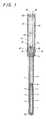
- the ceramic thermocouple for measuring the molten metal temperatureuses an outer protecting tube 1 (second protecting tube) as an external protection means, in which an inner protecting tube 2 (first protecting tube) is sealed, in order to improve heat resistance and resistance against loss by melting or melt-away resistance.
- Tungsten-rhenium alloy strands (W-Re alloy strands) 6, 7extend into both the inner protecting tube 2 and the outer protecting tube 1.
- the outer protecting tube 1 and the inner protecting tube 2are filled with porous members 3, 4 made mainly of silicon nitride porous material to prevent breakage of the W-Re strands 6, 7 due to oxidation corrosion.
- the inner protecting tube 2is made of ceramics chosen from among silicon nitride (Si 3 N 4 ), sialon (Si-Al-O-N) and silicon carbide (SiC).
- the outer protecting tube 1is made from a carbide-based cermet or nitride-based cermet, with Mo as a base.
- the coatingmay be selected from Mo-ZrO 2 , Mo-ZrB 2 and Mo-ZrN. The coating produces a similar effect to that of the outer protecting tube 1, and thus is designated with the same reference numeral 1 as the outer protecting tube.
- the ceramic thermocouplemainly comprises: an inner protecting tube 2 made of the above ceramics; an outer protective means such as outer protecting tube 1 or coating 1 provided outside the inner protecting tube 2 to enclose it (the outer protective means will be representatively referred to as the outer protecting tube 1); a pair of W-Re strands 6, 7 of dissimilar compositions which form a temperature measuring portion at a joint portion 20 at the front end of, and inside, the inner protecting tube 2; porous members 3, 4 made mainly of silicon nitride and filled in the inner protecting tube 2 and the outer protecting tube 1 in such a way as to contain the W-Re strands 6, 7; and a first sealing member 9 provided at the end of the outer protecting tube 1 to seal the interior of the outer protecting tube 1.
- a part of the outer protecting tube 1 that accommodates the inner protecting tube 2constitutes a portion that enters into an object to be measured, such as molten metal.
- the outer protecting tube 1 forming the outer shell and made of cermetin particular has excellent heat resistance and melt-away resistance and, if cracked by thermal shock, will lead to a gradual break and not result in a catastrophic destruction as is observed with an outer shell made of, for example, ceramics.
- the outer protecting tube 1is either cemented or nitrided to increase its hardness.
- the inner protecting tube 2 sealed in the outer protecting tube 1is made of ceramics having silicon nitride as a main component.
- the inner protecting tube 2is kept out of direct contact with the molten iron and thus can be reduced in heat transfer coefficient, which in turn prevents breakage of the inner protecting tube 2 due to thermal impacts.
- the ceramic thermocouplecan be constructed so that the total heat capacity of the outer protecting tube 1 and the inner protecting tube 2 is small, forming the protecting tube in a two-layer structure does not reduce the temperature measurement responsiveness.
- a heat resisting glass layer 5is provided between the inner protecting tube 2 and the outer protecting tube 1 and thus can improve a fixed temperature thermal conductivity between the outer protecting tube 1 and the inner protecting tube 2. Particularly when a crack develops in the outer protecting tube 1, the heat resisting glass layer 5 infiltrates into the cracked portion filling a space in the crack and thereby preventing a catastrophic destruction of the outer protecting tube 1.
- the first sealing member provided at the end of the outer protecting tube 1is constructed in a two-layer structure comprising a dense heat resisting member 9 of, for example, silicon nitride and a heat resisting glass member 10 arranged in contact with the heat resisting member 9. Further, at the end of the inner protecting tube 2 is provided a sealing member 8 of dense heat resisting material, such as heat resisting glass and silicon nitride, that hermetically seals the interior of the inner protecting tube 2.
- the sealing member 8is hermetically fitted in the end of the inner protecting tube 2 and the heat resisting member 9 of silicon nitride and the heat resisting glass member 10 are hermetically fitted at the end of the outer protecting tube 1.
- the inert gas such as N 2 and Ar sealed in the interior of the outer protecting tube 1 and the inner protecting tube 2prevents oxidation of the W-Re strands 6, 7.
- the heat conductivity of the porous member 3 filled in the outer protecting tube 1is smaller than that of the porous member 4 filled in the inner protecting tube 2.
- the porous member 3may, for example, be constructed to have a greater number of pores than the porous member 4 to make its heat conductivity smaller.
- the end of the outer protecting tube 1is mounted with a metal pipe 11 through a fixing ring 14, the metal pipe 11 being filled with ceramic fibers 12.
- the outer protecting tube 1is secured with the fixing ring 14, which is fixed to the metal pipe 11 by fittings 16.
- the ceramic fibers 12may, for example, be formed of ceramic fibers such as SiC whiskers or a Si 3 N 4 -based reaction-sintered ceramics.
- the ends of the W-Re strands 6, 7are each connected with compensation conductors 13 extending into the metal pipe 11.
- the W-Re strands 6, 7 drawn out of the outer protecting tube 1are connected to the paired compensation conductors 13 by connection screws 17.
- One of the compensation conductors 13forms a plus terminal 18 and the other a minus terminal 19.
- the end of the metal pipe 11is sealed with a double silicon nitride plug 15.
- the paired W-Re strands 6, 7comprise two W-5Re and W-26Re strands with different compositions, both of which are 0.5 mm in diameter and 300 mm in length and are welded together at their front ends to form a joint portion 20.
- the W-Re strands 6, 7were padded with raw material powder mainly of silicon nitride and then installed in the inner protecting tube 2 of silicon nitride 6.5 mm in outer diameter and 120-150 mm in length, after which the above raw material powder is filled in the inner protecting tube 2.
- An inert gasis injected into the inner protecting tube 2 and the end of the inner protecting tube 2 was sealed with the sealing member 8 of heat resisting glass.
- the inner protecting tube 2was inserted into the outer protecting tube made of cermet of Mo/ZrO 2 which has an inner diameter of 7 mm, and the clearance between the outer protecting tube 1 and the inner protecting tube 2 was filled with heat resisting glass to fix them together with the heat resisting glass layer 5. Further, the outer protecting tube 1 is filled with a raw material powder mainly of silicon nitride mixed with a large amount of fibers to form many pores therein and at the same time injected with an inert gas. The end of the outer protecting tube 1 was sealed with the heat resisting member 9 and the heat resisting glass member 10, both forming a sealing member.
- thermocoupleIn addition to the above temperature measurements of molten cast iron, measurements were also taken successively of the temperature of molten metal, which was about 1500°C, by using the above ceramic thermocouple. More than 500 hours after the start of the temperature measurements, no anomalies such as changes in the electromotive force of the ceramic thermocouple were observed. That is, this ceramic thermocouple was found to have an excellent heat resistance and an excellent melt-away resistance.
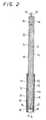
- this ceramic thermocouplehas the temperature measuring area of the protecting tube 21 (first protecting tube) covered with a protecting tube 22 (third protecting tube) as an outer protecting tube in the temperature measuring area to improve heat resistance and melt-away resistance.
- the tungsten-rhenium alloy strands (W-Re strands) 26, 27comprise a W-5Re strand 26 and a W-26Re strand 27, both extending along and inside the protecting tube 21 and spaced apart from each other.
- the tungsten-rhenium alloy strands 26,27are connected together at one end to form a temperature measuring portion 29 in the protecting tube 21 and at the other end are connected with terminals 32, 33 extending from the end of the protecting tube 21.
- the protecting tube 21is filled with a filler member 23 of porous silicon nitride ceramics.
- This ceramic thermocouple for the molten metal temperature measurementmainly comprises: a protecting tube 21; a pair of tungsten-rhenium alloy strands 26, 27 of dissimilar compositions installed in the protecting tube 21; a filler member 23 of porous silicon nitride ceramics filled in the protecting tube 21 to embed the tungsten-rhenium alloy strands 26, 27; a protecting tube 22 made of cermet containing Mo-which has a melt-away resistance as a base and arranged outside the temperature measuring portion 29 of the protecting tube 21 with its open end portion 30 projecting from the protecting tube 21; and a sealing member 28 made of dense heat resisting member and heat resisting glass that seals the end of the protecting tube 21.
- the protecting tube 21is made of ceramics selected from silicon nitride (Si 3 N 4 ), sialon and, where appropriate, silicon carbide (SiC).
- the protecting tube 22is made of carbide cermet with Mo as a base (Mo-ZrO 2 ).
- a coating 24is formed by flame spraying using a composite material of Mo as a base scattered with ZrN and/or ZrB 2 .
- An intermediate layer 25 of glassmainly SiO 2 , is formed in a clearance between the protecting tube 21 and the protecting tube 22.
- the interior of the protecting tube 21is filled with an inert gas such as Ar and N 2 to prevent oxidation of the tungsten-rhenium alloy strands 26, 27.
- an inert gassuch as Ar and N 2 to prevent oxidation of the tungsten-rhenium alloy strands 26, 27.
- the air inside the open end portion 30 of the protecting tube 22 projecting from the front end portion 34 of the protecting tube 21is sealed in the open end portion 30 when immersed in the molten iron, thus preventing the entry of the molten iron into the open end portion 30.
- the temperature measuring region at the front end portionis formed in a two-layer structure by the protecting tube 21 and the protecting tube 22 arranged outside the protecting tube 21 to make the heat capacity and the heat passage area of the front end portion 34 as small as possible to reduce the heat transfer to a rear end portion 35 of the protecting tube 21.
- the protecting tube 22 made of cermetin particular excels in the heat resistance and the melt-away resistance, and cracks, if produced in the protecting tube 22 by thermal shocks, lead to a slow destruction and do not result in a catastrophic destruction as is observed with the conventional ceramic outer shell.
- the protecting tube 21 sealed in the protecting tube 22is made from ceramics having silicon nitride as a major component. Silicon nitride, when exposed to molten iron, reacts with iron and is heavily melted away exhibiting a less thermal impact resistance than that of the cermet. However, because the protecting tube 21 does not directly contact the molten iron, its thermal transfer coefficient can be made small thus preventing the protecting tube 21 from being broken by thermal impacts.
- the total heat capacity of the protecting tube 21, the protecting tube 22 and the coating 24can be made small, so constructing the front end portion of the temperature measuring region in the two-layer structure does not deteriorate the temperature measurement responsiveness.
- the intermediate layer 25is provided between the protecting tube 21 and the protecting tube 22 and therefore can improve the fixed temperature heat conductivity between the protecting tube 21 and the protecting tube 22.
- the sealing member 28 provided at the rear end portion of the protecting tube 21is constructed in a two-layer structure comprising a dense heat resisting member of silicon nitride and a heat resisting glass member arranged in contact with the heat resisting member.
- the interior of the protecting tube 21is sealed with an inert gas such as N 2 and Ar during the process of filling the porous member 3.
- the end of the protecting tube 21is fitted gas-tightly with the sealing member 28.
- the filler member 23 filled in the protecting tube 21is formed in a porous structure made from Si 3 N 4 -based reaction-sintered ceramics with its thermal conductivity made small.
- the thermal conductivity of the filler member 23can be reduced, for example, by providing many pores in the filler member.
- this ceramic thermocouplecan have a reduced heat capacity in the temperature measuring region-where the protecting tube 21 is situated-that is submerged in the molten iron, preventing heat conduction from the temperature measuring region to the rear region.
- the paired W-Re strands 26, 27comprise a W-5Re strand 26 and a W-26Re strand 27 of different compositions, both having a wire diameter of 0.5 mm and a length of 300 mm. They are welded together at the front end to form a joint portion 36.
- the W-Re strands 26, 27were padded with raw material powder having silicon nitride as a main component.
- the protecting tube 21was made of silicon nitride, 6.5 mm in outer diameter and 120-150 mm in length, with the front end portion 34 closed and the rear end portion 35 open.
- the W-Re strands 26, 27 padded with the raw material powderwere inserted from the open rear end portion 35 of the protecting tube 21 and installed inside the protecting tube 21.
- the space in the protecting tube 21was filled with the raw material powder.
- the interior of the protecting tube 21was also injected with an inert gas such as Ar and N 2 and then the rear end portion 35 of the protecting tube 21 was hermetically closed by the sealing member 28 of heat resisting glass.
- the protecting tube 22was made of cermet containing Mo as a base and ZrO 2 and formed to have an inner diameter of 7 mm.
- a coating 24was formed on the outer circumferential surface of the protecting tube 22 by flame spraying using a composite material of Mo as a base scattered with ZrN and/or ArB 2 .
- the protecting tube 21was inserted into the protecting tube 22 sprayed with the coating 24.
- the protecting tube 22was arranged so that its open end portion 30 projected from the front end portion 34 of the protecting tube 21 to form an air chamber 31.
- the glass layer 25 of heat resistant glassis filled in a clearance between the protecting tube 21 and the protecting tube 22 to fix them together and the end portions of the protecting tubes are fixed and sealed with glass.
- this ceramic thermocouple(of this invention) measurements were taken of the molten cast iron, which was about 1450°C. At this time it took about 8 seconds for the raw material powder to be fired and stabilized, and measurement of the molten iron was cycled 500 times. Cracks were observed in the protecting tube 22 but had no adverse effects on the temperature measuring performance. In this state more than 1000 measurements were taken of the temperature of molten cast iron. No changes were detected in the electromotive force of the ceramic thermocouple and the temperature measurements were able to be performed stably.
- thermocoupleFor comparison with this molten metal temperature measuring ceramic thermocouple (of this invention), a thermocouple was manufactured to have a structure in which the W-Re strands padded with the raw material powder are inserted into a protecting tube of silicon nitride 7 mm in inner diameter.
- the thermocouple manufactured for comparisonwas evaluated in terms of the responsiveness, the ease with which the molten iron sticks to the thermocouple and the durability. The evaluation has found that the responsiveness is slower than the thermocouple of this invention as shown in Figure 4 and that iron is more likely to stick to the silicon nitride protecting tube.
- the molten metal temperature measuring thermocouple of the third embodimenthas the temperature measuring region of a protecting tube 41 (first protecting tube) covered through a heat insulating layer 45 by a protecting tube 42 (fourth protecting tube) as an outer protecting tube in the temperature measuring region to improve the heat resistance and the melt-away resistance.
- This thermocouplemainly comprises: a protecting tube 41 closed at one end and open at the other end; a heat resistant coating 44 formed over the outer surface of the protecting tube 41, having a small thermal expansion coefficient and hardly reacting with iron; a pair of temperature sensing alloy strands 46, 47 of differing compositions arranged in the protecting tube 41 and joined together at a front end joint portion 56 to form a temperature measuring portion 49; a filler member 43 filled in the protecting tube 41 to embed the alloy strands 46, 47; a sealing member 48 of dense heat resisting glass sealing the open end portion of the protecting tube 41, with the alloy strands 46, 47 drawn out therethrough; and a protecting tube 42 mounted over the outer circumferential surface of the protecting tube 41 through a heat insulating layer 45.
- the protecting tube 41is made of ceramics selected from silicon nitride (Si 3 N 4 ), sialon, cermet (Mo-ZrO 2 ) with Mo as a base and, where appropriate, silicon carbide (SiC).
- the protecting tube 41is formed in a size of 5 mm or less, for example, 3.5 mm in outer diameter.
- the protecting tube 42is made of cermet with Mo as a base (Mo-ZrO 2 ).
- the coating 44 sprayed over the outer circumferential surface of the protecting tube 41is formed of any one of Mo-ZrN, Mo-ZrB 2 and Mo-ZrO 2 that have small thermal expansion coefficients and hardly react with iron, or a combination of these.
- the outer circumferential surfacemay be flame-sprayed, as in the case of the protecting tube 41, with a coating of Mo-ZrN and/or Mo-ZrB 2 which have small thermal expansion coefficients and hardly react with iron.
- the sealing member 48is formed of a dense heat resistant glass and seals the end of the protecting tube 41.
- the paired alloy strands of dissimilar compositions arranged inside the protecting tube 41are tungsten-rhenium alloy strands comprising a W-5Re strand 46 and a W-26Re strand 47.
- the W-5Re strand 46 and the W-26Re strand 47are arranged to extend spaced apart inside the protecting tube 41.
- the front end portions of the W-5Re strand 46 and the W-26Re strand 47are joined together to form the temperature measuring portion 49.
- the other ends of these strandsare connected with terminals 52, 53 that extend from the end of the protecting tube 41.
- the terminals 52, 53are connected with leads 65 (compensation conductors) in kovar tubes 64 extending from the sealing member 48 at the end of the protecting tube 41.
- the heat insulating layer 45 formed in a space between the protecting tube 41 and the protecting tube 42is formed of a layer containing a large amount of air or ceramic fibers such as silicon carbide fibers to prevent the outflow of heat from the side surface of the protecting tube 41.
- the protecting tube 41is supported inside the protecting tube 42 by support rings 57 of silicon nitride arranged spaced apart in the heat insulating layer 45.
- the heat insulating layer 45serves to prevent heat from flowing out from the outer circumferential surface of the protecting tube 41 and allows the heat capacity of the protecting tube 41 to be made as small as possible.
- the ends of the protecting tube 41 and the protecting tube 42are secured to a metal pipe 58 as a stainless steel support rod by a collet chuck 62 having a tapered surface with a slit 63.
- the metal pipe 58is constructed in a two-layer structure, in which an inner metal pipe 58 is secured with the collet chuck 62 having a tapered outer surface and an outer metal pipe 58 is secured with a collet chuck 60 having a tapered inner surface.
- the metal pipe 58is formed at its end portion with a thread 67, over which a fixing nut 66 is screwed through a leaf spring 59.
- the interior of the protecting tube 41is filled with the filler member 43 and also injected with an inert gas such as Ar and N 2 to prevent breakage of the W-Re strands 46, 47 due to oxidation corrosion.
- the filler member 43is formed of porous silicon nitride ceramics with an additive of Ti (reaction-sintered silicon nitride ceramics) or heat resisting glass containing P, Si 3 N 4 , SiO 2 , Fe 2 O 3 , Cr 2 O 3 and the like.
- the front end portion 54 of the protecting tube 41is arranged to project slightly from the open end portion 50 of the protecting tube 42. With the thermocouple immersed in the molten metal, the open end portion 50 is sealed by the molten metal itself, sealing the air trapped between the protecting tube 41 and the protecting tube 42, thereby preventing the molten metal from entering between the protecting tube 41 and the protecting tube 42.
- the temperature measuring region of the front end portion 54 of the protecting tube 41is constructed in a two-layer structure that includes the protecting tube 41 and the protecting tube 42 arranged on the outer side of the protecting tube 41. This allows the heat capacity and the heat passage area of the front end portion 54 to be made as small as possible to reduce heat transfer to the rear end portion 55 of the protecting tube 41.
- the protecting tube 42 made of cermethas excellent heat and melt-away resistances and, if cracks are formed, the presence of the heat insulating layer 45 ensures that the cracks by thermal impact will lead to a slow destruction rather than a catastrophic destruction as is observed with the conventional ceramic outer shell.
- the protecting tube 41 inserted in the protecting tube 42is made from ceramics having silicon nitride as a main component. When exposed to molten metal such as iron, silicon nitride reacts with iron and is heavily melted away, so that its resistance to thermal impacts is not as high as that of cermet. But because the protecting tube 41 is kept out of direct contact with the molten iron, the thermal conductivity of the protecting tube 41 can be made small to prevent it from being destroyed by the thermal impacts.
- thermocouplefor the molten metal temperature measurement, because the total heat capacity of the protecting tube 41 and the heat resistant coating 44 can be made small, constructing the front end portion of the temperature measurement region in a two-layer structure will not degrade the responsiveness of the temperature measurement.
- the sealing member 48 provided at the rear end portion of the protecting tube 41is formed of a dense heat resistant glass member. During the process of filling the filler member 43, the interior of the protecting tube 41 is injected with an inert gas such as N 2 and Ar. The end of the protecting tube 41 is then hermetically fitted with the sealing member 48 to seal the injected gas.
- the filler member 43 filled in the protecting tube 41is made of a material such as Si 3 N 4 -based reaction-sintered ceramics in a porous structure with its thermal conductivity made small.
- the thermal conductivity of the filler member 43can be reduced, for example, by providing many pores in the filler member.
- this ceramic thermocouplecan have a reduced heat-capacity in the temperature measuring region-where the protecting tube 41 is situated-that is submerged in the molten iron, preventing heat conduction from the temperature measuring region to the rear region.
- the paired W-Re strands 46, 47comprise a W-5Re strand 46 and a W-26Re strand 47 of different compositions, both having a wire diameter of 0.2 mm and a length of 200 mm. They are welded together at the front end to form a joint portion 56.
- the W-Re strands 46, 47were padded with raw material powder of heat resistant glass having Si 3 N 4 powder as a main component.
- the protecting tube 41was made from silicon nitride, 3.5 mm in outer diameter and 120-150 mm in length, with the front end portion 54 closed and the rear end portion 55 open.
- the coating 44 of Mo-ZrN and Mo-ZrB 2is flame-sprayed over the outer surface of the protecting tube 41.
- the W-Re strands 46, 47 padded with the raw material powderwere inserted from the open rear end portion 55 of the protecting tube 41 and installed inside the protecting tube 41. Further, the interior in the protecting tube 41 was injected with an inert gas of Ar and N 2 and then the rear end portion 55 of the protecting tube 41 was hermetically sealed by the sealing member 48 of heat resistant, dense glass.
- the protecting tube 42is made from cermet of Mo as a base and ZrO 2 and formed to a size of 10 mm in outer diameter and 7 mm in inner diameter.
- the coating of composite material of Mo as a base scattered with ZrN and/or ZrB 2is flame-sprayed over the outer circumferential surface of the protecting tube 42.
- the protecting tube 41was inserted into the protecting tube 42 sprayed with the coating. At this time, the protecting tube 41 was inserted so that its front end portion 54 slightly projected from the open end portion 50 of the protecting tube 42.
- the support rings 57are arranged at intervals between the protecting tube 41 and the protecting tube 42 to form air chambers 51 between the protecting tube 41 and the protecting tube 42.
- the air chambers 51are filled with a heat insulating material to form a heat insulating layer 45.
- the end portions of the protecting tube 41 and the protecting tube 42are secured to the metal pipe 58 of stainless steel by the collet chuck 62.
- thermocoupleof this invention
- measurementswere made of the temperature of molten cast iron, which was about 1450°C. It took about 4 seconds for the raw material powder forming the filler member 43 to be fired and stabilized, and measurement of the molten cast iron was cycled 500 times.
- the thermocouple of this inventioncracks were observed in the protecting tube 42 after 500 cycles of temperature measurement of the cast iron but there was no problem with the molten cast iron temperature measurement performance. In this state, another 1000 or more measurements were taken of the temperature of the molten cast iron. It was verified that temperature measurements were able to be performed normally with no changes found in the electromotive force of the thermocouple.
- thermocoupleFor comparison with this molten metal temperature measuring thermocouple (of this invention), a thermocouple was manufactured to have a structure in which the W-Re strands padded with the raw material powder are inserted into the protecting tube of cermet 13 mm in outer diameter.
- the thermocouple manufactured for comparisonwas evaluated in terms of the responsiveness, the ease with which the molten iron sticks to the thermocouple and the durability. The evaluation has found that the responsiveness is slower than the thermocouple of this invention because of its larger outer diameter, with no response within 5 seconds. This shows that to improve the responsiveness the outer diameter of the protecting tube 41 should preferably be set to 5 mm or less.
Landscapes
- Physics & Mathematics (AREA)
- General Physics & Mathematics (AREA)
- Measuring Temperature Or Quantity Of Heat (AREA)
Abstract
Description
The present invention relates to a ceramicthermocouple with a protecting tube for measuring thetemperature of molten metal such as iron and castiron.
A thermocouple that has been in use to measurethe temperature of molten cast iron at about 1500 °Ccomprises Pt-Rh strands-which have a high meltingpoint and are stable in the atmosphere-and a paperpipe to which the Pt-Rh strands are secured. Such athermocouple becomes unable to make accuratemeasurement after taking one or two temperaturemeasurements of molten cast iron, and it is currentpractice to discard the used thermocouple.The thermocouple, because it cannot be usedrepetitively a number of times, is very expensive.
A sheath type thermocouple is known to have ofstrands made of chromel-alumel(CA), Pt-Rh and the same,and a metal sheath type protecting tube made of such metal as stainless steel (SUS) that is used athigh temperatures. Some stainless steel sheath typethermocouples can not be used in an atmosphere 1000 °Cor higher. In that case, they are made of a specialheat resisting alloy such as inconel.
There is also a thermocouple that is known tohave a structure in which Pt-Rh strands are installedin a protecting tube made of cermet.
Japanese Patent Laid-Open No. 160200/1994discloses a sheath type thermocouple with a gas-tightterminal. This thermocouple does not cause measuringerrors even when a temperature gradient is produced atthe terminal portion by transient temperaturevariations. Thermocouple strands of dissimilar metals-alumelwire and chromel wire-are installed in thestainless steel sheath and insulated from each other byan inorganic insulating material. The base end side ofthe sheath is hermetically sealed by the gas-tightterminal portion. The gas-tight terminal portion hasa ceramic end plate which is mounted with two kovarpiercing pipes, in which insulating sleeves areinserted. The thermocouple strands are individuallydrawn out through these insulating sleeves withoutdirectly contacting the piercing pipes.
The thermocouples have the following thermoelectromotive forces according to the types.The PR (Pt-Rh) thermocouple has a thermoelectromotiveforce of 1.241 mV at 500°C and 4.833 mV at 1000 °C. TheCA (chromel-alumel) thermocouple has athermoelectromotive force of 20.64 mV at 500°C and41.269 mV at 1000 °C. Further, the W-Re thermocouplehas a thermoelectromotive force of 8.655 mV at 500°Cand 18.257 mV at 1000 °C.
The Pt-Rh thermocouple cannot be used in aninert gas ambient and its service temperature in theatmosphere is 1500°C at the maximum. The CAthermocouple can be used in both the atmosphere andthe inert gas ambient and has the maximum servicetemperature of 800°C. Further, the W-Re thermocoupleis used in principle in the atmosphere and the inertgas ambient and has the maximum service temperature of400 °C in the atmosphere and 2300 °C(the highest) inthe inert gas ambient.
As to the PR thermocouple using the Pt-Rhstrands, because its thermoelectromotive force is assmall as about 1/15 that of the CA thermocouple andabout 1/7 that of the W-Re thermocouple, there is adrawback that its measuring precision is lower andresponsiveness slower than the latter twothermocouples. Hence, to measure the temperature of the blast furnace, a worker is forced to stay at themeasuring site near the smelting furnace for abouteight seconds until the temperature of the furnacestabilizes.
Moreover, the conventional thermocouples haveanother drawback that, during the measurement, moltenmetal such as iron and cast iron adheres to thethermocouples, which deteriorates the responsivenessof the thermocouples and requires a complex process ofremoving the adhering metal. A further drawback isthat the existing thermocouples have a life of onlyabout two measurements and their replacement takestime and labor. The W-Re strands of the thermocoupleare easily oxidized in the atmosphere and cannot beused for measuring the temperature of molten castiron. Still another problem is that molten ironeasily sticks to the outer protecting tube.
It is an aim of this invention to solve theabove problems and to provide a molten metaltemperature measuring ceramic thermocouple in whichfront ends of a pair of metal strands of dissimilarcompositions are joined together to form a temperaturemeasuring point and the paired metal strands areinstalled in a ceramic first protecting tube filled with a porous member, and in which the firstprotecting tube is contained in an outer protectivemeans of cermet having Mo as a base, therebypreventing reaction of the ceramics with the molteniron, improving heat resistance, resistance againstloss by melting or melt-away resistance and corrosionresistance, enabling repetitive use of thethermocouple.
Another aim of this invention is to improvethe responsiveness and durability and to provide amolten metal temperature measuring thermocouple inwhich the heat capacity of the front end portion ofthe thermocouple and the escape of heat to the rearand the side of the first protecting tube are made assmall as possible in order to concentrate the heat ofthe molten metal on the temperature measuring point atthe front end portion of the thermocouple in a shorttime; and in which the heat passage area is reduced,the thermocouple is constructed in a heat insulatingstructure, and the material of the thermocouple hassufficient durability and heat resistance and hardlyreacts with iron.
This invention relates to a ceramic thermocouplefor measuring the temperature of molten metal, whichcomprises: a first protecting tube made of any one of ceramics of silicon nitride and sialon; an outerprotective means made of cermet with Mo as a base andprovided on the outside of the first protecting tube;a pair of metal strands of dissimilar compositionsjoined together at a front end portion of, and inside,the first protecting tube to form a temperaturemeasuring portion; filler members of nonconductiveceramics filled in the first protecting tube tocontain the strands therein; and first sealing membersprovided at an end of the first protecting tube toseal the interior of the first protecting tube.
The materials forming the metal strands aretungsten-rhenium alloys.
To prevent oxidation of the metal strands, aninert gas such as N2 and Ar is sealed in the firstprotecting tube. Thus the strands installed in theinner protecting tube and the outer protective meansare free from oxidation, improving their heatresistance and durability. That is, because the W-Restrands are sealed in an inert gas, the thermalelectromotive force of the W-Re strands is relativelylarge, giving a good temperature responsiveness. TheW-Re strands have a melting point of 3000°C and arenot melted in molten cast iron.
Further, the filler members are made of a porous ceramics having silicon nitride as a main component.Alternatively, the filler members are reaction-sinteredsilicon nitride having Ti added thereto. Orthe filler members are a dehydration condensed heatresistant glass containing P, SiO2 and the like.
In this molten metal temperature measuringceramic thermocouple, the first protecting tube madeof ceramics such as silicon nitride is enclosed andprotected by the outer protective means as an outershell made of cermet having Mo as a base. Because thefirst protecting tube is not in direct contact withthe molten metal, ceramics is free from reaction withmolten iron, thereby improving heat resistance andmelt-away resistance. This enables the thermocoupleto measure the temperature of an object such as moltenmetal with high precision and swiftness even afterrepetitive use, thus prolonging the life of thethermocouple. The temperature measuring region islimited by the porous member in the first protectingtube to make it difficult for the heat of thetemperature measuring region to escape through theinside of the outer protective means toward the rear.This in turn allows the heat capacity of thetemperature measuring region to be reduced, improvingthe temperature measuring response of the thermocouple.
The outer protective means is formed as thesecond protecting tube or the coating, and is providedat its end with the second sealing members that sealthe interior of the outer protective means.
The first sealing members provided at the end ofthe outer protective means comprise dense, heatresisting members and heat resisting glass membersplaced in contact with the heat resisting members.
A heat resisting glass layer is provided betweenthe first protecting tube and the outer protectivemeans. That is, because the heat resisting glasslayer is arranged on the inner wall surface of theouter protective means, if cracks develop in the outerprotective means, the heat resisting glass layer fillsin the spaces in the cracks, thus preventing acatastrophic destruction even when the cermet of thefirst protecting tube is cracked due to thermalimpacts. This in turn prevents the first protectingtube of ceramics from directly contacting the molteniron, improving the heat resistance and melt-awayresistance.
The first protecting tube is installed inside theouter protective means and the portion of the interiorof the outer protective means where the first protecting tube is not present is filled with a porousmember which in turn is injected with an inert gassuch as N2 and Ar.
The thermal conductivity of the porous memberfilled in the outer protective means is set smallerthan that of the filler members filled in the firstprotecting tube. Hence, the thermal conduction to theoutside through the interior of the outer protectivemeans is suppressed, allowing the heat capacity of thetemperature measuring region of the thermocouple to bemade small and improving the responsiveness of thethermocouple.
The outer protective means is treated either withcementation or nitration. The outer protective meanstherefore has an increased hardness, an enhancedstrength against external forces, and an improveddurability.
The part of the outer protective means providedon the outer side of the first protecting tubeconstitutes a portion that is immersed in the moltenmetal.
The outer protective means is fitted at its endwith a metal pipe filled with ceramic fibers.Further, the ends of the metal strands are eachconnected with compensation conductors extending through the metal pipe.
The coating such as flame-sprayed coating as theexternal protective means is formed of any one, or acombination, of Mo-ZrO2, Mo-ZrB2 and Mo-ZrN, all thesehaving small thermal expansion coefficients and hardlyreacting with iron.
In this molten metal temperature measuringceramic thermocouple, the outer protective meanscomprises a third protecting tube arranged on theouter side of the temperature measuring portion of thefirst protecting tube with its open end portionprojecting from the first protecting tube and made ofthe cermet having melt-away resistance. The firstsealing members are formed of dense, heat resistingmembers and heat resisting glass. Hence, the airpresent in the open end portion of the thirdprotecting tube protruding from the end of the firstprotecting tube is trapped in the open end portionwhen immersed in the molten iron, thus preventing themolten iron from entering the open end portion.
The outer circumferential surface of the thirdprotecting tube is formed with a coating, which ismade of a material having Mo as a base scattered withone of ZrB2 and ZrN, both having small thermalexpansion coefficients and hardly reacting with iron.
A heat resisting glass layer containing SiO2 as amain component is formed in a space between the firstprotecting tube and the third protecting tube. Theheat resisting glass layer, if cracks are formed inthe outer protective means due to thermal impacts,fills in the cracks and thereby prevents the innerprotecting tube from directly contacting the moltenmetal, improving the durability.
The air present in the open end portion of thethird protecting tube projecting from the end of thefirst protecting tube is trapped in the open endportion when immersed in the molten iron, thuspreventing entry of the molten iron into the open endportion.
The front end portion of the temperaturemeasuring portion is constructed in a two-layerstructure comprising the first protecting tube and thethird protecting tube arranged on the outside of thefirst protecting tube, and a heat capacity and a heatpassage area of the front end portion are made assmall as possible to reduce heat conduction to a rearportion of the first protecting tube.
The outer protective means is a fourth protectingtube made of cermet having Mo as a base and mountedover the first protecting tube through a heat insulating layer, and a coating having a small thermalexpansion coefficient and hardly reacting with iron isarranged on an outer surface of the first protectingtube.
The first protecting tube is formed into asize 5mm or less in diameter.
The heat insulating layer interposed between thefirst protecting tube and the fourth protecting tubecomprises a heat insulating air layer and ceramicfibers to prevent an outflow of heat from a sidesurface of the first protecting tube.
End portions of the first protecting tube and thefourth protecting tube opposite the temperaturemeasuring portion are secured to a metal support pipeby a collet chuck with a space between the firstprotecting tube and the fourth protecting tube closed.
As described above, the molten metal temperaturemeasuring ceramic thermocouple has the firstprotecting tube made as small in diameter as possibleand formed of a heat resisting material such assilicon nitride, with its surface flame-sprayed with acoating that is hardly wetted with metal such as iron.This construction prevents breakage of the slenderfirst protecting tube and the escape of heat from theside surface of the fifth protecting tube. Provided around the first protecting tube is the heat resistantouter cylinder or the fourth protecting tube. Theheat insulating layer comprising an air layer andceramic fibers is provided between the firstprotecting tube and the fourth protecting tube.Although the front end portion of the fourthprotecting tube and the first protecting tube is open,the air layer is enclosed when the thermocouple isimmersed in the molten metal, preventing the moltenmetal from entering between the two protecting tubes.Thus the heat insulating effect is produced. Thediameters of the alloy strands are made as small aspossible to prevent heat from escaping through thestrands.
Now, embodiments of the ceramic thermocouple formeasuring the temperature of molten metal according tothis invention will be described by referring to theaccompanying drawings.
First, let us turn to Figure 1 to describe thefirst embodiment of the ceramic thermocouple formeasuring the molten metal temperature according tothis invention.
As shown in Figure 1, the ceramic thermocouplefor measuring the molten metal temperature uses anouter protecting tube 1 (second protecting tube) as anexternal protection means, in which an innerprotecting tube 2 (first protecting tube) is sealed,in order to improve heat resistance and resistanceagainst loss by melting or melt-away resistance.Tungsten-rhenium alloy strands (W-Re alloy strands) 6, 7 extend into both the inner protecting tube 2 and theouter protecting tube 1. The outer protecting tube 1and the inner protecting tube 2 are filled withporousmembers Re strands 6, 7due to oxidation corrosion. The inner protecting tube2 is made of ceramics chosen from among siliconnitride (Si3N4), sialon (Si-Al-O-N) and silicon carbide(SiC). The outer protecting tube 1 is made from acarbide-based cermet or nitride-based cermet, with Moas a base. When the outer protective means is formedof a coating such as spray coating, the coating may beselected from Mo-ZrO2, Mo-ZrB2 and Mo-ZrN. The coatingproduces a similar effect to that of the outerprotecting tube 1, and thus is designated with thesame reference numeral 1 as the outer protecting tube.
The ceramic thermocouple mainly comprises: aninner protecting tube 2 made of the above ceramics; anouter protective means such as outer protecting tube 1or coating 1 provided outside the inner protectingtube 2 to enclose it (the outer protective means willbe representatively referred to as the outerprotecting tube 1); a pair of W-Re strands 6, 7 ofdissimilar compositions which form a temperaturemeasuring portion at a joint portion 20 at the front end of, and inside, the inner protecting tube 2;porous members Restrands 6, 7; and a first sealing member 9 provided atthe end of the outer protecting tube 1 to seal theinterior of the outer protecting tube 1. A part ofthe outer protecting tube 1 that accommodates theinner protecting tube 2 constitutes a portion thatenters into an object to be measured, such as moltenmetal.
In this ceramic thermocouple, the outerprotecting tube 1 forming the outer shell and made ofcermet in particular has excellent heat resistance andmelt-away resistance and, if cracked by thermal shock,will lead to a gradual break and not result in acatastrophic destruction as is observed with an outershell made of, for example, ceramics. Further, theouter protecting tube 1 is either cemented or nitridedto increase its hardness. The inner protecting tube 2sealed in the outer protecting tube 1 is made ofceramics having silicon nitride as a main component.Although silicon nitride reacts with iron and isheavily melted away exhibiting a less thermal impactresistance than that of cermet, the inner protecting tube 2 is kept out of direct contact with the molteniron and thus can be reduced in heat transfercoefficient, which in turn prevents breakage of theinner protecting tube 2 due to thermal impacts.
Because the ceramic thermocouple can beconstructed so that the total heat capacity of theouter protecting tube 1 and the inner protecting tube2 is small, forming the protecting tube in a two-layerstructure does not reduce the temperature measurementresponsiveness. Further, a heat resistingglass layer 5 is provided between the inner protecting tube 2 andthe outer protecting tube 1 and thus can improve afixed temperature thermal conductivity between theouter protecting tube 1 and the inner protecting tube2. Particularly when a crack develops in the outerprotecting tube 1, the heat resistingglass layer 5infiltrates into the cracked portion filling a spacein the crack and thereby preventing a catastrophicdestruction of the outer protecting tube 1.
The first sealing member provided at the end ofthe outer protecting tube 1 is constructed in a two-layerstructure comprising a dense heat resistingmember 9 of, for example, silicon nitride and a heatresistingglass member 10 arranged in contact with theheat resisting member 9. Further, at the end of the inner protecting tube 2 is provided a sealingmember 8of dense heat resisting material, such as heatresisting glass and silicon nitride, that hermeticallyseals the interior of the inner protecting tube 2. Toseal an inert gas such as N2 and Ar inside the outerprotecting tube 1 and the inner protecting tube 2, thesealingmember 8 is hermetically fitted in the end ofthe inner protecting tube 2 and the heat resistingmember 9 of silicon nitride and the heat resistingglass member 10 are hermetically fitted at the end ofthe outer protecting tube 1. The inert gas such as N2and Ar sealed in the interior of the outer protectingtube 1 and the inner protecting tube 2 preventsoxidation of the W-Re strands 6, 7.
The heat conductivity of theporous member 3filled in the outer protecting tube 1 is smaller thanthat of theporous member 4 filled in the innerprotecting tube 2. Theporous member 3 may, forexample, be constructed to have a greater number ofpores than theporous member 4 to make its heatconductivity smaller. Hence, with this ceramicthermocouple, the heat capacity of the temperaturemeasuring part that accommodates the inner protectingtube 2 and which is to be inserted in a molten metalsuch as iron can be made small, thus blocking the heat conduction from the temperature measuring part to therear part.
The end of the outer protecting tube 1 is mountedwith a metal pipe 11 through a fixing ring 14, themetal pipe 11 being filled with ceramic fibers 12.The outer protecting tube 1 is secured with the fixingring 14, which is fixed to the metal pipe 11 byfittings 16. The ceramic fibers 12 may, for example,be formed of ceramic fibers such as SiC whiskers or aSi3N4-based reaction-sintered ceramics. The ends ofthe W-Re strands 6, 7 are each connected withcompensation conductors 13 extending into the metalpipe 11. The W-Re strands 6, 7 drawn out of the outerprotecting tube 1 are connected to the pairedcompensation conductors 13 by connection screws 17.One of thecompensation conductors 13 forms aplusterminal 18 and the other a minus terminal 19. Theend of the metal pipe 11 is sealed with a doublesilicon nitride plug 15.
In the first embodiment, the paired W-Re strands 6, 7 comprise two W-5Re and W-26Re strands withdifferent compositions, both of which are 0.5 mm indiameter and 300 mm in length and are welded togetherat their front ends to form a joint portion 20.First, the W-Re strands 6, 7 were padded with raw material powder mainly of silicon nitride and theninstalled in the inner protecting tube 2 of siliconnitride 6.5 mm in outer diameter and 120-150 mm inlength, after which the above raw material powder isfilled in the inner protecting tube 2. An inert gasis injected into the inner protecting tube 2 and theend of the inner protecting tube 2 was sealed with thesealingmember 8 of heat resisting glass.
Next, the inner protecting tube 2 was insertedinto the outer protecting tube made of cermet ofMo/ZrO2 which has an inner diameter of 7 mm, and theclearance between the outer protecting tube 1 and theinner protecting tube 2 was filled with heat resistingglass to fix them together with the heat resistingglass layer 5. Further, the outer protecting tube 1is filled with a raw material powder mainly of siliconnitride mixed with a large amount of fibers to formmany pores therein and at the same time injected withan inert gas. The end of the outer protecting tube 1was sealed with the heat resisting member 9 and theheat resistingglass member 10, both forming a sealingmember. Then, the ends of the W-Re strands 6, 7 wereconnected with thecompensation conductors 13, and theouter protecting tube 1 was securely mounted with thefixing ring 14, which was connected with the metal pipe 11 of, say, stainless steel. Next, ceramicfibers were filled in the interior of the metal pipe11, the end of which was sealed with theplug 15. Inthis way the ceramic thermocouple for measuring themolten metal temperature was manufactured.
Using the above molten metal temperaturemeasuring ceramic thermocouple, measurements were madeof the temperature of molten cast iron, which wasapproximately 1450°C. It took about 10 seconds forthe raw material powder to be fired and stabilized,and this cycle of measurement was repeated 200 times.Cracks were observed in the outer protecting tube 1but had no adverse effects on the temperaturemeasuring performance. In this state more than 1000measurements were taken of the temperature of moltencast iron. No changes were detected in theelectromotive force of the ceramic thermocouple andthe temperature measurements were able to be performedstably.
In addition to the above temperature measurementsof molten cast iron, measurements were also takensuccessively of the temperature of molten metal, whichwas about 1500°C, by using the above ceramicthermocouple. More than 500 hours after the start ofthe temperature measurements, no anomalies such as changes in the electromotive force of the ceramicthermocouple were observed. That is, this ceramicthermocouple was found to have an excellent heatresistance and an excellent melt-away resistance.
Next, referring to Figures 2, 3 and 4, the secondembodiment of the ceramic thermocouple for the moltenmetal temperature measurement according to thisinvention will be described.
As shown in Figure 2, this ceramic thermocouplehas the temperature measuring area of the protectingtube 21 (first protecting tube) covered with aprotecting tube 22 (third protecting tube) as an outerprotecting tube in the temperature measuring area toimprove heat resistance and melt-away resistance. Thetungsten-rhenium alloy strands (W-Re strands) 26, 27comprise a W-5Re strand 26 and a W-26Re strand 27,both extending along and inside the protectingtube 21and spaced apart from each other. The tungsten-rheniumalloy strands temperature measuring portion 29 inthe protectingtube 21 and at the other end areconnected withterminals tube 21. To prevent breakage of theW-Re strands tube 21 is filled with afiller member 23 of porous silicon nitride ceramics.
This ceramic thermocouple for the molten metaltemperature measurement mainly comprises: a protectingtube 21; a pair of tungsten-rhenium alloy strands tube 21; afiller member 23 of poroussilicon nitride ceramics filled in the protectingtube 21 to embed the tungsten-rhenium alloy strands tube 22 made of cermet containing Mo-whichhas a melt-away resistance as a base andarranged outside thetemperature measuring portion 29of the protectingtube 21 with itsopen end portion 30projecting from the protectingtube 21; and a sealingmember 28 made of dense heat resisting member and heatresisting glass that seals the end of the protectingtube 21.
The protectingtube 21 is made of ceramicsselected from silicon nitride (Si3N4), sialon and,where appropriate, silicon carbide (SiC). Theprotectingtube 22 is made of carbide cermet with Moas a base (Mo-ZrO2). On the outer circumferentialsurface of the protecting tube 22 acoating 24 isformed by flame spraying using a composite material ofMo as a base scattered with ZrN and/or ZrB2.
Anintermediate layer 25 of glass, mainly SiO2, is formed in a clearance between the protectingtube 21 and the protectingtube 22. Thus, if cracksdevelop in the cermet of the protectingtube 22, theglass of theintermediate layer 25 fills in the spacein the cracks. Further, if cermet is cracked bythermal impacts, this does not result in acatastrophic destruction of the protectingtube 22.
The interior of the protectingtube 21 is filledwith an inert gas such as Ar and N2 to preventoxidation of the tungsten-rhenium alloy strands
The air inside theopen end portion 30 of theprotectingtube 22 projecting from thefront endportion 34 of the protectingtube 21 is sealed in theopen end portion 30 when immersed in the molten iron,thus preventing the entry of the molten iron into theopen end portion 30.
The temperature measuring region at the front endportion is formed in a two-layer structure by theprotectingtube 21 and the protectingtube 22 arrangedoutside the protectingtube 21 to make the heatcapacity and the heat passage area of thefront endportion 34 as small as possible to reduce the heattransfer to arear end portion 35 of the protectingtube 21.
The protectingtube 22 made of cermet inparticular excels in the heat resistance and the melt-awayresistance, and cracks, if produced in theprotectingtube 22 by thermal shocks, lead to a slowdestruction and do not result in a catastrophicdestruction as is observed with the conventionalceramic outer shell. The protectingtube 21 sealed inthe protectingtube 22 is made from ceramics havingsilicon nitride as a major component. Siliconnitride, when exposed to molten iron, reacts with ironand is heavily melted away exhibiting a less thermalimpact resistance than that of the cermet. However,because the protectingtube 21 does not directlycontact the molten iron, its thermal transfercoefficient can be made small thus preventing theprotectingtube 21 from being broken by thermalimpacts.
With this thermocouple, the total heat capacityof the protectingtube 21, the protectingtube 22 andthecoating 24 can be made small, so constructing thefront end portion of the temperature measuring regionin the two-layer structure does not deteriorate thetemperature measurement responsiveness. Further, theintermediate layer 25 is provided between theprotectingtube 21 and the protectingtube 22 and therefore can improve the fixed temperature heatconductivity between the protectingtube 21 and theprotectingtube 22. When cracks develop in theprotectingtube 22, the glass infiltrates into thecracked portion filling in spaces in the cracks thuspreventing a catastrophic destruction of theprotectingtube 22.
The sealingmember 28 provided at the rear endportion of the protectingtube 21 is constructed in atwo-layer structure comprising a dense heat resistingmember of silicon nitride and a heat resisting glassmember arranged in contact with the heat resistingmember. The interior of the protectingtube 21 issealed with an inert gas such as N2 and Ar during theprocess of filling theporous member 3. The end ofthe protectingtube 21 is fitted gas-tightly with thesealingmember 28.
Thefiller member 23 filled in the protectingtube 21 is formed in a porous structure made fromSi3N4-based reaction-sintered ceramics with its thermalconductivity made small. The thermal conductivity ofthefiller member 23 can be reduced, for example, byproviding many pores in the filler member. Hence,this ceramic thermocouple can have a reduced heatcapacity in the temperature measuring region-where the protectingtube 21 is situated-that is submerged inthe molten iron, preventing heat conduction from thetemperature measuring region to the rear region.
In the second embodiment, the paired W-Re strands 5Re strand 26 and a W-26Re strand 27 of different compositions, both having a wirediameter of 0.5 mm and a length of 300 mm. They arewelded together at the front end to form ajointportion 36. The W-Re strands tube 21 was made of siliconnitride, 6.5 mm in outer diameter and 120-150 mm inlength, with thefront end portion 34 closed and therear end portion 35 open. The W-Re strands rear end portion 35 of the protectingtube 21and installed inside the protectingtube 21. Further,the space in the protectingtube 21 was filled withthe raw material powder. The interior of theprotectingtube 21 was also injected with an inert gassuch as Ar and N2 and then therear end portion 35 ofthe protectingtube 21 was hermetically closed by thesealingmember 28 of heat resisting glass.
The protectingtube 22 was made of cermetcontaining Mo as a base and ZrO2 and formed to have an inner diameter of 7 mm. Acoating 24 was formed onthe outer circumferential surface of the protectingtube 22 by flame spraying using a composite materialof Mo as a base scattered with ZrN and/or ArB2. Theprotectingtube 21 was inserted into the protectingtube 22 sprayed with thecoating 24. At this time,the protectingtube 22 was arranged so that itsopenend portion 30 projected from thefront end portion 34of the protectingtube 21 to form anair chamber 31.Next, theglass layer 25 of heat resistant glass isfilled in a clearance between the protectingtube 21and the protectingtube 22 to fix them together andthe end portions of the protecting tubes are fixed andsealed with glass.
Using this ceramic thermocouple (of thisinvention), measurements were taken of the molten castiron, which was about 1450°C. At this time it tookabout 8 seconds for the raw material powder to befired and stabilized, and measurement of the molteniron was cycled 500 times. Cracks were observed inthe protectingtube 22 but had no adverse effects onthe temperature measuring performance. In this statemore than 1000 measurements were taken of thetemperature of molten cast iron. No changes weredetected in the electromotive force of the ceramic thermocouple and the temperature measurements wereable to be performed stably.
In addition to the above temperature measurementsof molten cast iron, successive measurements were alsotaken of the temperature of molten metal, which wasabout 1500°C, by using the above ceramic thermocouple.More than 500 hours after the start of the temperaturemeasurements, no anomalies such as changes in theelectromotive force of the ceramic thermocouple wereobserved. That is, this ceramic thermocouple wasfound to have an excellent heat resistance and anexcellent melt-away resistance.
For comparison with this molten metal temperaturemeasuring ceramic thermocouple (of this invention), athermocouple was manufactured to have a structure inwhich the W-Re strands padded with the raw materialpowder are inserted into a protecting tube ofsiliconnitride 7 mm in inner diameter. The thermocouplemanufactured for comparison was evaluated in terms ofthe responsiveness, the ease with which the molteniron sticks to the thermocouple and the durability.The evaluation has found that the responsiveness isslower than the thermocouple of this invention asshown in Figure 4 and that iron is more likely tostick to the silicon nitride protecting tube.
Next, by referring to Figures 5 and 6, the thirdembodiment of the molten metal temperature measuringthermocouple according to this invention will bedescribed.
The molten metal temperature measuringthermocouple of the third embodiment has thetemperature measuring region of a protecting tube 41(first protecting tube) covered through aheatinsulating layer 45 by a protecting tube 42 (fourthprotecting tube) as an outer protecting tube in thetemperature measuring region to improve the heatresistance and the melt-away resistance. Thisthermocouple mainly comprises: a protectingtube 41closed at one end and open at the other end; a heatresistant coating 44 formed over the outer surface ofthe protectingtube 41, having a small thermalexpansion coefficient and hardly reacting with iron; apair of temperaturesensing alloy strands tube 41 and joined together at a front endjoint portion 56to form atemperature measuring portion 49; afillermember 43 filled in the protectingtube 41 to embedthealloy strands member 48 of denseheat resisting glass sealing the open end portion ofthe protectingtube 41, with thealloy strands tube 42mounted over the outer circumferential surface of theprotectingtube 41 through aheat insulating layer 45.
The protectingtube 41 is made of ceramicsselected from silicon nitride (Si3N4), sialon, cermet(Mo-ZrO2) with Mo as a base and, where appropriate,silicon carbide (SiC). The protectingtube 41 isformed in a size of 5 mm or less, for example, 3.5 mmin outer diameter. The protectingtube 42 is made ofcermet with Mo as a base (Mo-ZrO2). Thecoating 44sprayed over the outer circumferential surface of theprotectingtube 41 is formed of any one of Mo-ZrN, Mo-ZrB2and Mo-ZrO2 that have small thermal expansioncoefficients and hardly react with iron, or acombination of these. The outer circumferentialsurface may be flame-sprayed, as in the case of theprotectingtube 41, with a coating of Mo-ZrN and/orMo-ZrB2 which have small thermal expansioncoefficients and hardly react with iron. The sealingmember 48 is formed of a dense heat resistant glassand seals the end of the protectingtube 41.
The paired alloy strands of dissimilarcompositions arranged inside the protectingtube 41are tungsten-rhenium alloy strands comprising a W-5Restrand 46 and a W-26Re strand 47. The W-5Re strand 46 and the W-26Re strand 47 are arranged to extend spacedapart inside the protectingtube 41. The front endportions of the W-5Re strand 46 and the W-26Re strand 47 are joined together to form thetemperaturemeasuring portion 49. The other ends of these strandsare connected withterminals tube 41. Theterminals kovar tubes 64 extending from thesealingmember 48 at the end of the protectingtube 41.
Theheat insulating layer 45 formed in a spacebetween the protectingtube 41 and the protectingtube 42 is formed of a layer containing a large amount ofair or ceramic fibers such as silicon carbide fibersto prevent the outflow of heat from the side surfaceof the protectingtube 41. The protectingtube 41 issupported inside the protectingtube 42 by supportrings 57 of silicon nitride arranged spaced apart intheheat insulating layer 45. Theheat insulatinglayer 45 serves to prevent heat from flowing out fromthe outer circumferential surface of the protectingtube 41 and allows the heat capacity of the protectingtube 41 to be made as small as possible. The ends ofthe protectingtube 41 and the protectingtube 42 are secured to ametal pipe 58 as a stainless steelsupport rod by acollet chuck 62 having a taperedsurface with a slit 63.
In Figure 5, themetal pipe 58 is constructed ina two-layer structure, in which aninner metal pipe 58is secured with thecollet chuck 62 having a taperedouter surface and anouter metal pipe 58 is securedwith acollet chuck 60 having a tapered inner surface.Themetal pipe 58 is formed at its end portion with athread 67, over which a fixingnut 66 is screwedthrough aleaf spring 59. Fastening anut 61 fittedover thethread 67 of theinner metal pipe 58 againstthe force of theleaf spring 59 causes the slit 63 ofthecollet chuck 62 to be fastened elastically by thecollet chuck 60 and reduced in diameter, with theresult that thecollet chuck 62 tightens theprotectingtube 41.
The interior of the protectingtube 41 is filledwith thefiller member 43 and also injected with aninert gas such as Ar and N2 to prevent breakage of theW-Re strands filler member 43 is formed of porous silicon nitrideceramics with an additive of Ti (reaction-sinteredsilicon nitride ceramics) or heat resisting glasscontaining P, Si3N4, SiO2, Fe2O3, Cr2O3 and the like.
Thefront end portion 54 of the protectingtube 41 is arranged to project slightly from the open endportion 50 of the protectingtube 42. With thethermocouple immersed in the molten metal, the openend portion 50 is sealed by the molten metal itself,sealing the air trapped between the protectingtube 41and the protectingtube 42, thereby preventing themolten metal from entering between the protectingtube 41 and the protectingtube 42. The temperaturemeasuring region of thefront end portion 54 of theprotectingtube 41 is constructed in a two-layerstructure that includes the protectingtube 41 and theprotectingtube 42 arranged on the outer side of theprotectingtube 41. This allows the heat capacity andthe heat passage area of thefront end portion 54 tobe made as small as possible to reduce heat transferto therear end portion 55 of the protectingtube 41.
Further, the protectingtube 42 made of cermethas excellent heat and melt-away resistances and, ifcracks are formed, the presence of theheat insulatinglayer 45 ensures that the cracks by thermal impactwill lead to a slow destruction rather than acatastrophic destruction as is observed with theconventional ceramic outer shell. The protectingtube 41 inserted in the protectingtube 42 is made from ceramics having silicon nitride as a main component.When exposed to molten metal such as iron, siliconnitride reacts with iron and is heavily melted away,so that its resistance to thermal impacts is not ashigh as that of cermet. But because the protectingtube 41 is kept out of direct contact with the molteniron, the thermal conductivity of the protectingtube 41 can be made small to prevent it from beingdestroyed by the thermal impacts.
With this thermocouple for the molten metaltemperature measurement, because the total heatcapacity of the protectingtube 41 and the heatresistant coating 44 can be made small, constructingthe front end portion of the temperature measurementregion in a two-layer structure will not degrade theresponsiveness of the temperature measurement. Thesealingmember 48 provided at the rear end portion ofthe protectingtube 41 is formed of a dense heatresistant glass member. During the process of fillingthefiller member 43, the interior of the protectingtube 41 is injected with an inert gas such as N2 andAr. The end of the protectingtube 41 is thenhermetically fitted with the sealingmember 48 to sealthe injected gas.
Thefiller member 43 filled in the protectingtube 41 is made of a material such as Si3N4-basedreaction-sintered ceramics in a porous structure withits thermal conductivity made small. The thermalconductivity of thefiller member 43 can be reduced,for example, by providing many pores in the fillermember. Hence, this ceramic thermocouple can have areduced heat-capacity in the temperature measuringregion-where the protectingtube 41 is situated-thatis submerged in the molten iron, preventing heatconduction from the temperature measuring region tothe rear region.
In the third embodiment, the paired W-Re strands 5Re strand 46 and a W-26Re strand 47 of different compositions, both having a wirediameter of 0.2 mm and a length of 200 mm. They arewelded together at the front end to form ajointportion 56. The W-Re strands tube 41 was made from silicon nitride, 3.5 mm in outerdiameter and 120-150 mm in length, with thefront endportion 54 closed and therear end portion 55 open.Thecoating 44 of Mo-ZrN and Mo-ZrB2 is flame-sprayedover the outer surface of the protectingtube 41. TheW-Re strands rear end portion 55of the protectingtube 41 and installed inside theprotectingtube 41. Further, the interior in theprotectingtube 41 was injected with an inert gas ofAr and N2 and then therear end portion 55 of theprotectingtube 41 was hermetically sealed by thesealingmember 48 of heat resistant, dense glass.
The protectingtube 42 is made from cermet of Moas a base and ZrO2 and formed to a size of 10 mm inouter diameter and 7 mm in inner diameter. Thecoating of composite material of Mo as a basescattered with ZrN and/or ZrB2 is flame-sprayed overthe outer circumferential surface of the protectingtube 42. The protectingtube 41 was inserted into theprotectingtube 42 sprayed with the coating. At thistime, the protectingtube 41 was inserted so that itsfront end portion 54 slightly projected from the openend portion 50 of the protectingtube 42. The supportrings 57 are arranged at intervals between theprotectingtube 41 and the protectingtube 42 to formair chambers 51 between the protectingtube 41 and theprotectingtube 42. Theair chambers 51 are filledwith a heat insulating material to form aheatinsulating layer 45. The end portions of theprotectingtube 41 and the protectingtube 42 are secured to themetal pipe 58 of stainless steel by thecollet chuck 62.
Using the molten metal temperature measuringthermocouple (of this invention) with the aboveconstruction, measurements were made of thetemperature of molten cast iron, which was about1450°C. It took about 4 seconds for the raw materialpowder forming thefiller member 43 to be fired andstabilized, and measurement of the molten cast ironwas cycled 500 times. In the thermocouple of thisinvention, cracks were observed in the protectingtube 42 after 500 cycles of temperature measurement of thecast iron but there was no problem with the moltencast iron temperature measurement performance. Inthis state, another 1000 or more measurements weretaken of the temperature of the molten cast iron. Itwas verified that temperature measurements were ableto be performed normally with no changes found in theelectromotive force of the thermocouple.
In addition to the above temperature measurementsof molten cast iron, successive measurements were alsotaken of the temperature of other molten metal, whichwas about 1500°C, by using the above ceramicthermocouple. More than 500 hours after the start ofthe temperature measurements, no anomalies such as changes in the electromotive force of the ceramicthermocouple were observed. That is, this ceramicthermocouple was found to have an excellent heatresistance and an excellent melt-away resistance.
For comparison with this molten metal temperaturemeasuring thermocouple (of this invention), athermocouple was manufactured to have a structure inwhich the W-Re strands padded with the raw materialpowder are inserted into the protecting tube ofcermet 13 mm in outer diameter. The thermocouplemanufactured for comparison was evaluated in terms ofthe responsiveness, the ease with which the molteniron sticks to the thermocouple and the durability.The evaluation has found that the responsiveness isslower than the thermocouple of this invention becauseof its larger outer diameter, with no response within5 seconds. This shows that to improve theresponsiveness the outer diameter of the protectingtube 41 should preferably be set to 5 mm or less.
Claims (26)
- A ceramic thermocouple for measuring thetemperature of molten metal comprising:a first protecting tube(2,21,214) made of any oneof ceramics of silicon nitride and sialon;an outer protective means(1,22,42,44) made ofcermet with Mo as a base and provided on the outside ofthe first protecting tube(2,21,24);a pair of metal strands(6,7,26,27,46,47) ofdissimilar compositions joined together at a front endportion of, and inside, the first protecting tube(2,21,41) to form a temperature measuring portion;filler members(3,4,23,43) of nonconductive ceramicsfilled in the first protecting tube(2,21,41) to containthe strands(6,7,26,27,46,47) therein; andfirst sealing members(8,28,48) provided at an endof the first protecting tube(2,21,41) to seal theinterior of the first protecting tube(2,21,41).
- A ceramic thermocouple for measuring thetemperature of molten metal according to claim 1,wherein the material forming the metal strands(6,7,26,27,46,47) is a tungsten-rhenium alloy.
- A ceramic thermocouple for measuring thetemperature of molten metal according to claim 1,wherein the interior of the first protecting tube(2,21, 41) is filled with an inert gas to prevent oxidation ofthe metal strands(6,7,26,27,46,47).
- A ceramic thermocouple for measuring thetemperature of molten metal according to claim 1,wherein the filler members(3,4,23,43) are a porousceramics having silicon nitride as a main component.
- A ceramic thermocouple for measuring thetemperature of molten metal according to claim 1,wherein the outer protective means(1) is formed as anyone of a second protecting tube(1) and a coating(1) andsecond sealing members(8) are provided at an end of theouter protective means(1) to seal the interior of theouter protective means(1).
- A ceramic thermocouple for measuring thetemperature of molten metal according to claim 5,wherein the second sealing members(9,10) provided atthe end of the outer protective means(1) comprise denseheat resisting members(9) and heat resisting glassmembers(10) placed in contact with the heat resistingmembers.
- A ceramic thermocouple for measuring thetemperature of molten metal according to claim 5,wherein a heat resisting glass layer(5) is providedbetween the first protecting tube(2) and the outerprotective means(1).
- A ceramic thermocouple for measuring thetemperature of molten metal according to claim 5,wherein the first protecting tube(2) is installed insidethe outer protective means(1), the interior of the outerprotective means(1) where the first protecting tube(2)is not present is filled with a porous member(3), andthe porous member(3) is injected with an inert gas of N2and Ar.
- A ceramic thermocouple for measuring thetemperature of molten metal according to claim 8,wherein a heat conductivity of the porous member(3)filled in the outer protective means(1) is smaller thanthat of the filler members(4) filled in the firstprotecting tube(2).
- A ceramic thermocouple for measuring thetemperature of molten metal according to claim 5,wherein the outer protective means(1) is treated witheither a cementation or a nitration.
- A ceramic thermocouple for measuring thetemperature of molten metal according to claim 5,wherein a part of the outer protective means(1)arranged on the outer side of the first protecting tube(2) constitutes a portion of the thermocouple to beimmersed in the molten metal.
- A ceramic thermocouple for measuring the temperature of molten metal according to claim 5,wherein the end of the outer protective means(1) isattached with a metal pipe(11) filled with ceramicfibers(12).
- A ceramic thermocouple for measuring thetemperature of molten metal according to claim 12,wherein ends of the metal strands(6,7) are connectedwith compensation conductors(13) extending through themetal pipe(11).
- A ceramic thermocouple for measuring thetemperature of molten metal according to claim 5,wherein the coating(1) forming the outer protectivemeans(1) is made of a material selected from Mo-ZrO2,Mo-ZrB2 and Mo-ZrN.
- A ceramic thermocouple for measuring thetemperature of molten metal according to claim 1,wherein the outer protective means(22) is a thirdprotecting tube(22) made of the cermet havingresistance against loss by melting or melt-awayresistance and arranged on the outside of thetemperature measuring portion(29) of the firstprotecting tube(21) with its open end portion(30)projecting from the first protecting tube(21), and thefirst sealing members(28) comprise dense heat resistingmembers and heat resisting glass.
- A ceramic thermocouple for measuring thetemperature of molten metal according to claim 15,wherein a coating(24) is formed over an outercircumferential surface of the third protecting tube(22), the coating(24) being made of a materialcomprising Mo as a base scattered with one of ZrB2 andZrN, both having small thermal expansion coefficientsand hardly reacting with iron.
- A ceramic thermocouple for measuring thetemperature of molten metal according to claim 15,wherein an intermediate layer(25) of glass containingSiO2 as a main component is formed in a space betweenthe first protecting tube(21) and the third protectingtube(22).
- A ceramic thermocouple for measuring thetemperature of molten metal according to claim 15,wherein air present in the open end portion(30) of thethird protecting tube(22) projecting from the end ofthe first protecting tube(21) is trapped hermeticallyinside the open end portion(30) when immersed in themolten iron to prevent the molten iron from enteringthe open end portion(30).
- A ceramic thermocouple for measuring thetemperature of molten metal according to claim 15,wherein a front end portion(34) of the temperature measuring portion is constructed in a two-layerstructure comprising the first protecting tube(21) andthe third protecting tube(22) arranged on the outsideof the first protecting tube(21), and a heat capacityand a heat passage area of the front end portion(34)are made as small as possible to reduce heat transferto a rear portion(35) of the first protecting tube(21).
- A ceramic thermocouple for measuring thetemperature of molten metal according to claim 1,wherein the outer protective means(42,44) is a fourthprotecting tube(42) made of cermet having Mo as a baseand mounted over the first protecting tube(41) througha heat insulating layer, and a coating(44) having asmall thermal expansion coefficient and hardly reactingwith iron is arranged on an outer surface of the firstprotecting tube(41).
- A ceramic thermocouple for measuring thetemperature of molten metal according to claim 20,wherein the coating(44) is a flame-sprayed coating madeof any one, or a combination, of Mo-ZrN, Mo-ZrB2 andMo-ZrO2, all having small thermal expansion coefficientsand hardly reacting with iron.
- A ceramic thermocouple for measuring thetemperature of molten metal according to claim 20,wherein the filler members(43) are reaction-sintered silicon nitride having an additive of Ti.
- A ceramic thermocouple for measuring thetemperature of molten metal according to claim 20,wherein the filler members(43) are a dehydrationcondensed-heat resisting glass containing P, SiO2 andthe like.
- A ceramic thermocouple for measuring thetemperature of molten metal according to claim 20,wherein the first protecting tube(41) is formed into asize of 5 mm or less in outer diameter.
- A ceramic thermocouple for measuring thetemperature of molten metal according to claim 20,wherein the heat insulating layer(45) interposedbetween the first protecting tube(41) and the fourthprotecting tube(42) comprises a heat insulating airlayer and ceramic fibers to prevent an outflow of heatfrom a side surface of the first protecting tube(41).
- A ceramic thermocouple for measuring thetemperature of molten metal according to claim 20,wherein end portions of the first protecting tube(41)and the fourth protecting tube(42) opposite thetemperature measuring portion are secured to a metalsupport pipe(58) by a collet chuck(62) with a spacebetween the first protecting tube(41) and the fourthprotecting tube(42) closed.
Applications Claiming Priority (6)
| Application Number | Priority Date | Filing Date | Title |
|---|---|---|---|
| JP18183897AJP3306425B2 (en) | 1997-06-24 | 1997-06-24 | Ceramic thermocouple for high temperature measurement |
| JP181838/97 | 1997-06-24 | ||
| JP227072/97 | 1997-08-11 | ||
| JP22707297AJP3603557B2 (en) | 1997-08-11 | 1997-08-11 | Ceramic thermocouple for measuring molten metal temperature |
| JP25797797AJP3306426B2 (en) | 1997-09-08 | 1997-09-08 | Thermocouple for measuring molten metal temperature |
| JP257977/97 | 1997-09-08 |
Publications (1)
| Publication Number | Publication Date |
|---|---|
| EP0887632A1true EP0887632A1 (en) | 1998-12-30 |
Family
ID=27325081
Family Applications (1)
| Application Number | Title | Priority Date | Filing Date |
|---|---|---|---|
| EP98304965AWithdrawnEP0887632A1 (en) | 1997-06-24 | 1998-06-24 | A ceramic thermocouple for measuring temperature of molten metal |
Country Status (1)
| Country | Link |
|---|---|
| EP (1) | EP0887632A1 (en) |
Cited By (364)
| Publication number | Priority date | Publication date | Assignee | Title |
|---|---|---|---|---|
| EP1150107A1 (en)* | 2000-04-24 | 2001-10-31 | Isuzu Ceramics Research Institute Co., Ltd. | Thermocouple-type temperature-detecting device |
| WO2004104534A1 (en)* | 2003-05-21 | 2004-12-02 | Rdc Contrôle Ltée | Composite ceramic device for measuring the temperature of liquids |
| DE102006034979A1 (en)* | 2006-07-28 | 2008-02-28 | Ust Umweltsensortechnik Gmbh | High temperature sensor for use in temperature measurement with high mechanical and thermal loads, e.g. in exhaust systems of motor vehicles, has temperature-dependent measuring resistor and four connection points arranged on support body |
| CN101034016B (en)* | 2007-04-04 | 2010-07-21 | 沈阳东大传感技术有限公司 | Special type WRe temperature sensor |
| WO2010129431A3 (en)* | 2009-05-06 | 2011-03-31 | Asm America, Inc. | Thermocouple and temperature measuring system |
| US8382370B2 (en) | 2009-05-06 | 2013-02-26 | Asm America, Inc. | Thermocouple assembly with guarded thermocouple junction |
| US8616765B2 (en) | 2008-12-08 | 2013-12-31 | Asm America, Inc. | Thermocouple |
| TWI424790B (en)* | 2005-06-09 | 2014-01-21 | Imura Internat U S A Inc | Radio frequency identification controlled heatable objects and tag assembly for radio frequency identification controlled heatable objects |
| USD702188S1 (en) | 2013-03-08 | 2014-04-08 | Asm Ip Holding B.V. | Thermocouple |
| US9297705B2 (en) | 2009-05-06 | 2016-03-29 | Asm America, Inc. | Smart temperature measuring device |
| US9648975B2 (en) | 2004-04-28 | 2017-05-16 | Imura International Usa, Inc. | Radio frequency identification controlled heatable objects |
| CN107144595A (en)* | 2017-06-06 | 2017-09-08 | 南昌大学 | Thermocouple and the repeatable cast aluminium alloy gold Sampling device for thermal analysis utilized of sampling cup |
| CN108645527A (en)* | 2018-05-15 | 2018-10-12 | 安徽天卓信息技术有限公司 | A kind of heat safe temperature sensor |
| US10229833B2 (en) | 2016-11-01 | 2019-03-12 | Asm Ip Holding B.V. | Methods for forming a transition metal nitride film on a substrate by atomic layer deposition and related semiconductor device structures |
| US10249524B2 (en) | 2017-08-09 | 2019-04-02 | Asm Ip Holding B.V. | Cassette holder assembly for a substrate cassette and holding member for use in such assembly |
| US10249577B2 (en) | 2016-05-17 | 2019-04-02 | Asm Ip Holding B.V. | Method of forming metal interconnection and method of fabricating semiconductor apparatus using the method |
| US10262859B2 (en) | 2016-03-24 | 2019-04-16 | Asm Ip Holding B.V. | Process for forming a film on a substrate using multi-port injection assemblies |
| US10269558B2 (en) | 2016-12-22 | 2019-04-23 | Asm Ip Holding B.V. | Method of forming a structure on a substrate |
| US10276355B2 (en) | 2015-03-12 | 2019-04-30 | Asm Ip Holding B.V. | Multi-zone reactor, system including the reactor, and method of using the same |
| US10283353B2 (en) | 2017-03-29 | 2019-05-07 | Asm Ip Holding B.V. | Method of reforming insulating film deposited on substrate with recess pattern |
| US10290508B1 (en) | 2017-12-05 | 2019-05-14 | Asm Ip Holding B.V. | Method for forming vertical spacers for spacer-defined patterning |
| US10312129B2 (en) | 2015-09-29 | 2019-06-04 | Asm Ip Holding B.V. | Variable adjustment for precise matching of multiple chamber cavity housings |
| US10312055B2 (en) | 2017-07-26 | 2019-06-04 | Asm Ip Holding B.V. | Method of depositing film by PEALD using negative bias |
| US10319588B2 (en) | 2017-10-10 | 2019-06-11 | Asm Ip Holding B.V. | Method for depositing a metal chalcogenide on a substrate by cyclical deposition |
| US10322384B2 (en) | 2015-11-09 | 2019-06-18 | Asm Ip Holding B.V. | Counter flow mixer for process chamber |
| US10340135B2 (en) | 2016-11-28 | 2019-07-02 | Asm Ip Holding B.V. | Method of topologically restricted plasma-enhanced cyclic deposition of silicon or metal nitride |
| US10340125B2 (en) | 2013-03-08 | 2019-07-02 | Asm Ip Holding B.V. | Pulsed remote plasma method and system |
| US10343920B2 (en) | 2016-03-18 | 2019-07-09 | Asm Ip Holding B.V. | Aligned carbon nanotubes |
| US10361201B2 (en) | 2013-09-27 | 2019-07-23 | Asm Ip Holding B.V. | Semiconductor structure and device formed using selective epitaxial process |
| US10364493B2 (en) | 2016-08-25 | 2019-07-30 | Asm Ip Holding B.V. | Exhaust apparatus and substrate processing apparatus having an exhaust line with a first ring having at least one hole on a lateral side thereof placed in the exhaust line |
| US10364496B2 (en) | 2011-06-27 | 2019-07-30 | Asm Ip Holding B.V. | Dual section module having shared and unshared mass flow controllers |
| US10366864B2 (en) | 2013-03-08 | 2019-07-30 | Asm Ip Holding B.V. | Method and system for in-situ formation of intermediate reactive species |
| US10367080B2 (en) | 2016-05-02 | 2019-07-30 | Asm Ip Holding B.V. | Method of forming a germanium oxynitride film |
| US10381226B2 (en) | 2016-07-27 | 2019-08-13 | Asm Ip Holding B.V. | Method of processing substrate |
| US10378106B2 (en) | 2008-11-14 | 2019-08-13 | Asm Ip Holding B.V. | Method of forming insulation film by modified PEALD |
| US10381219B1 (en) | 2018-10-25 | 2019-08-13 | Asm Ip Holding B.V. | Methods for forming a silicon nitride film |
| US10388509B2 (en) | 2016-06-28 | 2019-08-20 | Asm Ip Holding B.V. | Formation of epitaxial layers via dislocation filtering |
| US10388513B1 (en) | 2018-07-03 | 2019-08-20 | Asm Ip Holding B.V. | Method for depositing silicon-free carbon-containing film as gap-fill layer by pulse plasma-assisted deposition |
| US10395919B2 (en) | 2016-07-28 | 2019-08-27 | Asm Ip Holding B.V. | Method and apparatus for filling a gap |
| US10403504B2 (en) | 2017-10-05 | 2019-09-03 | Asm Ip Holding B.V. | Method for selectively depositing a metallic film on a substrate |
| US10410943B2 (en) | 2016-10-13 | 2019-09-10 | Asm Ip Holding B.V. | Method for passivating a surface of a semiconductor and related systems |
| US10435790B2 (en) | 2016-11-01 | 2019-10-08 | Asm Ip Holding B.V. | Method of subatmospheric plasma-enhanced ALD using capacitively coupled electrodes with narrow gap |
| US10438965B2 (en) | 2014-12-22 | 2019-10-08 | Asm Ip Holding B.V. | Semiconductor device and manufacturing method thereof |
| US10446393B2 (en) | 2017-05-08 | 2019-10-15 | Asm Ip Holding B.V. | Methods for forming silicon-containing epitaxial layers and related semiconductor device structures |
| US10458018B2 (en) | 2015-06-26 | 2019-10-29 | Asm Ip Holding B.V. | Structures including metal carbide material, devices including the structures, and methods of forming same |
| US10468262B2 (en) | 2017-02-15 | 2019-11-05 | Asm Ip Holding B.V. | Methods for forming a metallic film on a substrate by a cyclical deposition and related semiconductor device structures |
| US10468251B2 (en) | 2016-02-19 | 2019-11-05 | Asm Ip Holding B.V. | Method for forming spacers using silicon nitride film for spacer-defined multiple patterning |
| US10483099B1 (en) | 2018-07-26 | 2019-11-19 | Asm Ip Holding B.V. | Method for forming thermally stable organosilicon polymer film |
| US10480072B2 (en) | 2009-04-06 | 2019-11-19 | Asm Ip Holding B.V. | Semiconductor processing reactor and components thereof |
| US10504742B2 (en) | 2017-05-31 | 2019-12-10 | Asm Ip Holding B.V. | Method of atomic layer etching using hydrogen plasma |
| US10501866B2 (en) | 2016-03-09 | 2019-12-10 | Asm Ip Holding B.V. | Gas distribution apparatus for improved film uniformity in an epitaxial system |
| US10510536B2 (en) | 2018-03-29 | 2019-12-17 | Asm Ip Holding B.V. | Method of depositing a co-doped polysilicon film on a surface of a substrate within a reaction chamber |
| US10529563B2 (en) | 2017-03-29 | 2020-01-07 | Asm Ip Holdings B.V. | Method for forming doped metal oxide films on a substrate by cyclical deposition and related semiconductor device structures |
| US10529554B2 (en) | 2016-02-19 | 2020-01-07 | Asm Ip Holding B.V. | Method for forming silicon nitride film selectively on sidewalls or flat surfaces of trenches |
| US10529542B2 (en) | 2015-03-11 | 2020-01-07 | Asm Ip Holdings B.V. | Cross-flow reactor and method |
| US10535516B2 (en) | 2018-02-01 | 2020-01-14 | Asm Ip Holdings B.V. | Method for depositing a semiconductor structure on a surface of a substrate and related semiconductor structures |
| US10541173B2 (en) | 2016-07-08 | 2020-01-21 | Asm Ip Holding B.V. | Selective deposition method to form air gaps |
| US10541333B2 (en) | 2017-07-19 | 2020-01-21 | Asm Ip Holding B.V. | Method for depositing a group IV semiconductor and related semiconductor device structures |
| US10559458B1 (en) | 2018-11-26 | 2020-02-11 | Asm Ip Holding B.V. | Method of forming oxynitride film |
| US10561975B2 (en) | 2014-10-07 | 2020-02-18 | Asm Ip Holdings B.V. | Variable conductance gas distribution apparatus and method |
| US10566223B2 (en) | 2012-08-28 | 2020-02-18 | Asm Ip Holdings B.V. | Systems and methods for dynamic semiconductor process scheduling |
| US10590535B2 (en) | 2017-07-26 | 2020-03-17 | Asm Ip Holdings B.V. | Chemical treatment, deposition and/or infiltration apparatus and method for using the same |
| US10600673B2 (en) | 2015-07-07 | 2020-03-24 | Asm Ip Holding B.V. | Magnetic susceptor to baseplate seal |
| US10607895B2 (en) | 2017-09-18 | 2020-03-31 | Asm Ip Holdings B.V. | Method for forming a semiconductor device structure comprising a gate fill metal |
| US10604847B2 (en) | 2014-03-18 | 2020-03-31 | Asm Ip Holding B.V. | Gas distribution system, reactor including the system, and methods of using the same |
| US10605530B2 (en) | 2017-07-26 | 2020-03-31 | Asm Ip Holding B.V. | Assembly of a liner and a flange for a vertical furnace as well as the liner and the vertical furnace |
| US10612137B2 (en) | 2016-07-08 | 2020-04-07 | Asm Ip Holdings B.V. | Organic reactants for atomic layer deposition |
| US10612136B2 (en) | 2018-06-29 | 2020-04-07 | ASM IP Holding, B.V. | Temperature-controlled flange and reactor system including same |
| USD880437S1 (en) | 2018-02-01 | 2020-04-07 | Asm Ip Holding B.V. | Gas supply plate for semiconductor manufacturing apparatus |
| US10622375B2 (en) | 2016-11-07 | 2020-04-14 | Asm Ip Holding B.V. | Method of processing a substrate and a device manufactured by using the method |
| US10643826B2 (en) | 2016-10-26 | 2020-05-05 | Asm Ip Holdings B.V. | Methods for thermally calibrating reaction chambers |
| US10643904B2 (en) | 2016-11-01 | 2020-05-05 | Asm Ip Holdings B.V. | Methods for forming a semiconductor device and related semiconductor device structures |
| US10655221B2 (en) | 2017-02-09 | 2020-05-19 | Asm Ip Holding B.V. | Method for depositing oxide film by thermal ALD and PEALD |
| US10658181B2 (en) | 2018-02-20 | 2020-05-19 | Asm Ip Holding B.V. | Method of spacer-defined direct patterning in semiconductor fabrication |
| US10658205B2 (en) | 2017-09-28 | 2020-05-19 | Asm Ip Holdings B.V. | Chemical dispensing apparatus and methods for dispensing a chemical to a reaction chamber |
| US10665452B2 (en) | 2016-05-02 | 2020-05-26 | Asm Ip Holdings B.V. | Source/drain performance through conformal solid state doping |
| US10683571B2 (en) | 2014-02-25 | 2020-06-16 | Asm Ip Holding B.V. | Gas supply manifold and method of supplying gases to chamber using same |
| US10685834B2 (en) | 2017-07-05 | 2020-06-16 | Asm Ip Holdings B.V. | Methods for forming a silicon germanium tin layer and related semiconductor device structures |
| US10692741B2 (en) | 2017-08-08 | 2020-06-23 | Asm Ip Holdings B.V. | Radiation shield |
| US10707106B2 (en) | 2011-06-06 | 2020-07-07 | Asm Ip Holding B.V. | High-throughput semiconductor-processing apparatus equipped with multiple dual-chamber modules |
| US10714315B2 (en) | 2012-10-12 | 2020-07-14 | Asm Ip Holdings B.V. | Semiconductor reaction chamber showerhead |
| US10714385B2 (en) | 2016-07-19 | 2020-07-14 | Asm Ip Holding B.V. | Selective deposition of tungsten |
| US10714350B2 (en) | 2016-11-01 | 2020-07-14 | ASM IP Holdings, B.V. | Methods for forming a transition metal niobium nitride film on a substrate by atomic layer deposition and related semiconductor device structures |
| US10714335B2 (en) | 2017-04-25 | 2020-07-14 | Asm Ip Holding B.V. | Method of depositing thin film and method of manufacturing semiconductor device |
| US10734497B2 (en) | 2017-07-18 | 2020-08-04 | Asm Ip Holding B.V. | Methods for forming a semiconductor device structure and related semiconductor device structures |
| US10731249B2 (en) | 2018-02-15 | 2020-08-04 | Asm Ip Holding B.V. | Method of forming a transition metal containing film on a substrate by a cyclical deposition process, a method for supplying a transition metal halide compound to a reaction chamber, and related vapor deposition apparatus |
| US10734244B2 (en) | 2017-11-16 | 2020-08-04 | Asm Ip Holding B.V. | Method of processing a substrate and a device manufactured by the same |
| US10741385B2 (en) | 2016-07-28 | 2020-08-11 | Asm Ip Holding B.V. | Method and apparatus for filling a gap |
| US10755922B2 (en) | 2018-07-03 | 2020-08-25 | Asm Ip Holding B.V. | Method for depositing silicon-free carbon-containing film as gap-fill layer by pulse plasma-assisted deposition |
| US10770286B2 (en) | 2017-05-08 | 2020-09-08 | Asm Ip Holdings B.V. | Methods for selectively forming a silicon nitride film on a substrate and related semiconductor device structures |
| US10770336B2 (en) | 2017-08-08 | 2020-09-08 | Asm Ip Holding B.V. | Substrate lift mechanism and reactor including same |
| US10767789B2 (en) | 2018-07-16 | 2020-09-08 | Asm Ip Holding B.V. | Diaphragm valves, valve components, and methods for forming valve components |
| US10787741B2 (en) | 2014-08-21 | 2020-09-29 | Asm Ip Holding B.V. | Method and system for in situ formation of gas-phase compounds |
| US10797133B2 (en) | 2018-06-21 | 2020-10-06 | Asm Ip Holding B.V. | Method for depositing a phosphorus doped silicon arsenide film and related semiconductor device structures |
| US10804098B2 (en) | 2009-08-14 | 2020-10-13 | Asm Ip Holding B.V. | Systems and methods for thin-film deposition of metal oxides using excited nitrogen-oxygen species |
| US10811256B2 (en) | 2018-10-16 | 2020-10-20 | Asm Ip Holding B.V. | Method for etching a carbon-containing feature |
| US10818758B2 (en) | 2018-11-16 | 2020-10-27 | Asm Ip Holding B.V. | Methods for forming a metal silicate film on a substrate in a reaction chamber and related semiconductor device structures |
| USD900036S1 (en) | 2017-08-24 | 2020-10-27 | Asm Ip Holding B.V. | Heater electrical connector and adapter |
| US10829852B2 (en) | 2018-08-16 | 2020-11-10 | Asm Ip Holding B.V. | Gas distribution device for a wafer processing apparatus |
| US10832903B2 (en) | 2011-10-28 | 2020-11-10 | Asm Ip Holding B.V. | Process feed management for semiconductor substrate processing |
| US10847366B2 (en) | 2018-11-16 | 2020-11-24 | Asm Ip Holding B.V. | Methods for depositing a transition metal chalcogenide film on a substrate by a cyclical deposition process |
| US10847365B2 (en) | 2018-10-11 | 2020-11-24 | Asm Ip Holding B.V. | Method of forming conformal silicon carbide film by cyclic CVD |
| US10844484B2 (en) | 2017-09-22 | 2020-11-24 | Asm Ip Holding B.V. | Apparatus for dispensing a vapor phase reactant to a reaction chamber and related methods |
| US10847371B2 (en) | 2018-03-27 | 2020-11-24 | Asm Ip Holding B.V. | Method of forming an electrode on a substrate and a semiconductor device structure including an electrode |
| US10851456B2 (en) | 2016-04-21 | 2020-12-01 | Asm Ip Holding B.V. | Deposition of metal borides |
| US10854498B2 (en) | 2011-07-15 | 2020-12-01 | Asm Ip Holding B.V. | Wafer-supporting device and method for producing same |
| USD903477S1 (en) | 2018-01-24 | 2020-12-01 | Asm Ip Holdings B.V. | Metal clamp |
| US10858737B2 (en) | 2014-07-28 | 2020-12-08 | Asm Ip Holding B.V. | Showerhead assembly and components thereof |
| US10865475B2 (en) | 2016-04-21 | 2020-12-15 | Asm Ip Holding B.V. | Deposition of metal borides and silicides |
| US10867786B2 (en) | 2018-03-30 | 2020-12-15 | Asm Ip Holding B.V. | Substrate processing method |
| US10867788B2 (en) | 2016-12-28 | 2020-12-15 | Asm Ip Holding B.V. | Method of forming a structure on a substrate |
| US10872771B2 (en) | 2018-01-16 | 2020-12-22 | Asm Ip Holding B. V. | Method for depositing a material film on a substrate within a reaction chamber by a cyclical deposition process and related device structures |
| US10886123B2 (en) | 2017-06-02 | 2021-01-05 | Asm Ip Holding B.V. | Methods for forming low temperature semiconductor layers and related semiconductor device structures |
| US10883175B2 (en) | 2018-08-09 | 2021-01-05 | Asm Ip Holding B.V. | Vertical furnace for processing substrates and a liner for use therein |
| US10892156B2 (en) | 2017-05-08 | 2021-01-12 | Asm Ip Holding B.V. | Methods for forming a silicon nitride film on a substrate and related semiconductor device structures |
| US10896820B2 (en) | 2018-02-14 | 2021-01-19 | Asm Ip Holding B.V. | Method for depositing a ruthenium-containing film on a substrate by a cyclical deposition process |
| US10910262B2 (en) | 2017-11-16 | 2021-02-02 | Asm Ip Holding B.V. | Method of selectively depositing a capping layer structure on a semiconductor device structure |
| US10914004B2 (en) | 2018-06-29 | 2021-02-09 | Asm Ip Holding B.V. | Thin-film deposition method and manufacturing method of semiconductor device |
| US10923344B2 (en) | 2017-10-30 | 2021-02-16 | Asm Ip Holding B.V. | Methods for forming a semiconductor structure and related semiconductor structures |
| US10928731B2 (en) | 2017-09-21 | 2021-02-23 | Asm Ip Holding B.V. | Method of sequential infiltration synthesis treatment of infiltrateable material and structures and devices formed using same |
| US10934619B2 (en) | 2016-11-15 | 2021-03-02 | Asm Ip Holding B.V. | Gas supply unit and substrate processing apparatus including the gas supply unit |
| US10941490B2 (en) | 2014-10-07 | 2021-03-09 | Asm Ip Holding B.V. | Multiple temperature range susceptor, assembly, reactor and system including the susceptor, and methods of using the same |
| US10975470B2 (en) | 2018-02-23 | 2021-04-13 | Asm Ip Holding B.V. | Apparatus for detecting or monitoring for a chemical precursor in a high temperature environment |
| US11001925B2 (en) | 2016-12-19 | 2021-05-11 | Asm Ip Holding B.V. | Substrate processing apparatus |
| US11018002B2 (en) | 2017-07-19 | 2021-05-25 | Asm Ip Holding B.V. | Method for selectively depositing a Group IV semiconductor and related semiconductor device structures |
| US11015245B2 (en) | 2014-03-19 | 2021-05-25 | Asm Ip Holding B.V. | Gas-phase reactor and system having exhaust plenum and components thereof |
| US11018047B2 (en) | 2018-01-25 | 2021-05-25 | Asm Ip Holding B.V. | Hybrid lift pin |
| US11024523B2 (en) | 2018-09-11 | 2021-06-01 | Asm Ip Holding B.V. | Substrate processing apparatus and method |
| US11022879B2 (en) | 2017-11-24 | 2021-06-01 | Asm Ip Holding B.V. | Method of forming an enhanced unexposed photoresist layer |
| US11031242B2 (en) | 2018-11-07 | 2021-06-08 | Asm Ip Holding B.V. | Methods for depositing a boron doped silicon germanium film |
| USD922229S1 (en) | 2019-06-05 | 2021-06-15 | Asm Ip Holding B.V. | Device for controlling a temperature of a gas supply unit |
| US11049751B2 (en) | 2018-09-14 | 2021-06-29 | Asm Ip Holding B.V. | Cassette supply system to store and handle cassettes and processing apparatus equipped therewith |
| US11056567B2 (en) | 2018-05-11 | 2021-07-06 | Asm Ip Holding B.V. | Method of forming a doped metal carbide film on a substrate and related semiconductor device structures |
| US11053591B2 (en) | 2018-08-06 | 2021-07-06 | Asm Ip Holding B.V. | Multi-port gas injection system and reactor system including same |
| US11056344B2 (en) | 2017-08-30 | 2021-07-06 | Asm Ip Holding B.V. | Layer forming method |
| US11069510B2 (en) | 2017-08-30 | 2021-07-20 | Asm Ip Holding B.V. | Substrate processing apparatus |
| US11081345B2 (en) | 2018-02-06 | 2021-08-03 | Asm Ip Holding B.V. | Method of post-deposition treatment for silicon oxide film |
| US11087997B2 (en) | 2018-10-31 | 2021-08-10 | Asm Ip Holding B.V. | Substrate processing apparatus for processing substrates |
| US11088002B2 (en) | 2018-03-29 | 2021-08-10 | Asm Ip Holding B.V. | Substrate rack and a substrate processing system and method |
| US11114294B2 (en) | 2019-03-08 | 2021-09-07 | Asm Ip Holding B.V. | Structure including SiOC layer and method of forming same |
| US11114283B2 (en) | 2018-03-16 | 2021-09-07 | Asm Ip Holding B.V. | Reactor, system including the reactor, and methods of manufacturing and using same |
| USD930782S1 (en) | 2019-08-22 | 2021-09-14 | Asm Ip Holding B.V. | Gas distributor |
| US11127589B2 (en) | 2019-02-01 | 2021-09-21 | Asm Ip Holding B.V. | Method of topology-selective film formation of silicon oxide |
| US11127617B2 (en) | 2017-11-27 | 2021-09-21 | Asm Ip Holding B.V. | Storage device for storing wafer cassettes for use with a batch furnace |
| USD931978S1 (en) | 2019-06-27 | 2021-09-28 | Asm Ip Holding B.V. | Showerhead vacuum transport |
| US11139191B2 (en) | 2017-08-09 | 2021-10-05 | Asm Ip Holding B.V. | Storage apparatus for storing cassettes for substrates and processing apparatus equipped therewith |
| US11139308B2 (en) | 2015-12-29 | 2021-10-05 | Asm Ip Holding B.V. | Atomic layer deposition of III-V compounds to form V-NAND devices |
| US11158513B2 (en) | 2018-12-13 | 2021-10-26 | Asm Ip Holding B.V. | Methods for forming a rhenium-containing film on a substrate by a cyclical deposition process and related semiconductor device structures |
| US11171025B2 (en) | 2019-01-22 | 2021-11-09 | Asm Ip Holding B.V. | Substrate processing device |
| USD935572S1 (en) | 2019-05-24 | 2021-11-09 | Asm Ip Holding B.V. | Gas channel plate |
| DE102020113903B3 (en) | 2020-05-25 | 2021-11-18 | Temperaturmeßtechnik Geraberg GmbH | Thermocouple for measuring high temperatures and method for drift detection on a thermocouple |
| WO2021237470A1 (en)* | 2020-05-26 | 2021-12-02 | 王煜 | Thermocouple sensor with long service life |
| US11205585B2 (en) | 2016-07-28 | 2021-12-21 | Asm Ip Holding B.V. | Substrate processing apparatus and method of operating the same |
| US11217444B2 (en) | 2018-11-30 | 2022-01-04 | Asm Ip Holding B.V. | Method for forming an ultraviolet radiation responsive metal oxide-containing film |
| USD940837S1 (en) | 2019-08-22 | 2022-01-11 | Asm Ip Holding B.V. | Electrode |
| US11222772B2 (en) | 2016-12-14 | 2022-01-11 | Asm Ip Holding B.V. | Substrate processing apparatus |
| US11227789B2 (en) | 2019-02-20 | 2022-01-18 | Asm Ip Holding B.V. | Method and apparatus for filling a recess formed within a substrate surface |
| US11227782B2 (en) | 2019-07-31 | 2022-01-18 | Asm Ip Holding B.V. | Vertical batch furnace assembly |
| US11230766B2 (en) | 2018-03-29 | 2022-01-25 | Asm Ip Holding B.V. | Substrate processing apparatus and method |
| US11233133B2 (en) | 2015-10-21 | 2022-01-25 | Asm Ip Holding B.V. | NbMC layers |
| US11232963B2 (en) | 2018-10-03 | 2022-01-25 | Asm Ip Holding B.V. | Substrate processing apparatus and method |
| US11251068B2 (en) | 2018-10-19 | 2022-02-15 | Asm Ip Holding B.V. | Substrate processing apparatus and substrate processing method |
| US11251040B2 (en) | 2019-02-20 | 2022-02-15 | Asm Ip Holding B.V. | Cyclical deposition method including treatment step and apparatus for same |
| USD944946S1 (en) | 2019-06-14 | 2022-03-01 | Asm Ip Holding B.V. | Shower plate |
| US11270899B2 (en) | 2018-06-04 | 2022-03-08 | Asm Ip Holding B.V. | Wafer handling chamber with moisture reduction |
| US11274369B2 (en) | 2018-09-11 | 2022-03-15 | Asm Ip Holding B.V. | Thin film deposition method |
| US11282698B2 (en) | 2019-07-19 | 2022-03-22 | Asm Ip Holding B.V. | Method of forming topology-controlled amorphous carbon polymer film |
| US11286558B2 (en) | 2019-08-23 | 2022-03-29 | Asm Ip Holding B.V. | Methods for depositing a molybdenum nitride film on a surface of a substrate by a cyclical deposition process and related semiconductor device structures including a molybdenum nitride film |
| US11289326B2 (en) | 2019-05-07 | 2022-03-29 | Asm Ip Holding B.V. | Method for reforming amorphous carbon polymer film |
| US11286562B2 (en) | 2018-06-08 | 2022-03-29 | Asm Ip Holding B.V. | Gas-phase chemical reactor and method of using same |
| USD947913S1 (en) | 2019-05-17 | 2022-04-05 | Asm Ip Holding B.V. | Susceptor shaft |
| US11295980B2 (en) | 2017-08-30 | 2022-04-05 | Asm Ip Holding B.V. | Methods for depositing a molybdenum metal film over a dielectric surface of a substrate by a cyclical deposition process and related semiconductor device structures |
| USD948463S1 (en) | 2018-10-24 | 2022-04-12 | Asm Ip Holding B.V. | Susceptor for semiconductor substrate supporting apparatus |
| USD949319S1 (en) | 2019-08-22 | 2022-04-19 | Asm Ip Holding B.V. | Exhaust duct |
| US11306395B2 (en) | 2017-06-28 | 2022-04-19 | Asm Ip Holding B.V. | Methods for depositing a transition metal nitride film on a substrate by atomic layer deposition and related deposition apparatus |
| US11315794B2 (en) | 2019-10-21 | 2022-04-26 | Asm Ip Holding B.V. | Apparatus and methods for selectively etching films |
| US11339476B2 (en) | 2019-10-08 | 2022-05-24 | Asm Ip Holding B.V. | Substrate processing device having connection plates, substrate processing method |
| US11342216B2 (en) | 2019-02-20 | 2022-05-24 | Asm Ip Holding B.V. | Cyclical deposition method and apparatus for filling a recess formed within a substrate surface |
| US11345999B2 (en) | 2019-06-06 | 2022-05-31 | Asm Ip Holding B.V. | Method of using a gas-phase reactor system including analyzing exhausted gas |
| US11355338B2 (en) | 2019-05-10 | 2022-06-07 | Asm Ip Holding B.V. | Method of depositing material onto a surface and structure formed according to the method |
| US11361990B2 (en) | 2018-05-28 | 2022-06-14 | Asm Ip Holding B.V. | Substrate processing method and device manufactured by using the same |
| US11374112B2 (en) | 2017-07-19 | 2022-06-28 | Asm Ip Holding B.V. | Method for depositing a group IV semiconductor and related semiconductor device structures |
| US11378337B2 (en) | 2019-03-28 | 2022-07-05 | Asm Ip Holding B.V. | Door opener and substrate processing apparatus provided therewith |
| US11393690B2 (en) | 2018-01-19 | 2022-07-19 | Asm Ip Holding B.V. | Deposition method |
| US11390945B2 (en) | 2019-07-03 | 2022-07-19 | Asm Ip Holding B.V. | Temperature control assembly for substrate processing apparatus and method of using same |
| US11390946B2 (en) | 2019-01-17 | 2022-07-19 | Asm Ip Holding B.V. | Methods of forming a transition metal containing film on a substrate by a cyclical deposition process |
| US11401605B2 (en) | 2019-11-26 | 2022-08-02 | Asm Ip Holding B.V. | Substrate processing apparatus |
| US11414760B2 (en) | 2018-10-08 | 2022-08-16 | Asm Ip Holding B.V. | Substrate support unit, thin film deposition apparatus including the same, and substrate processing apparatus including the same |
| US11424119B2 (en) | 2019-03-08 | 2022-08-23 | Asm Ip Holding B.V. | Method for selective deposition of silicon nitride layer and structure including selectively-deposited silicon nitride layer |
| US11430674B2 (en) | 2018-08-22 | 2022-08-30 | Asm Ip Holding B.V. | Sensor array, apparatus for dispensing a vapor phase reactant to a reaction chamber and related methods |
| US11430640B2 (en) | 2019-07-30 | 2022-08-30 | Asm Ip Holding B.V. | Substrate processing apparatus |
| US11437241B2 (en) | 2020-04-08 | 2022-09-06 | Asm Ip Holding B.V. | Apparatus and methods for selectively etching silicon oxide films |
| US11443926B2 (en) | 2019-07-30 | 2022-09-13 | Asm Ip Holding B.V. | Substrate processing apparatus |
| US11447864B2 (en) | 2019-04-19 | 2022-09-20 | Asm Ip Holding B.V. | Layer forming method and apparatus |
| US11447861B2 (en) | 2016-12-15 | 2022-09-20 | Asm Ip Holding B.V. | Sequential infiltration synthesis apparatus and a method of forming a patterned structure |
| USD965044S1 (en) | 2019-08-19 | 2022-09-27 | Asm Ip Holding B.V. | Susceptor shaft |
| USD965524S1 (en) | 2019-08-19 | 2022-10-04 | Asm Ip Holding B.V. | Susceptor support |
| US11469098B2 (en) | 2018-05-08 | 2022-10-11 | Asm Ip Holding B.V. | Methods for depositing an oxide film on a substrate by a cyclical deposition process and related device structures |
| US11476109B2 (en) | 2019-06-11 | 2022-10-18 | Asm Ip Holding B.V. | Method of forming an electronic structure using reforming gas, system for performing the method, and structure formed using the method |
| US11473195B2 (en) | 2018-03-01 | 2022-10-18 | Asm Ip Holding B.V. | Semiconductor processing apparatus and a method for processing a substrate |
| US11482412B2 (en) | 2018-01-19 | 2022-10-25 | Asm Ip Holding B.V. | Method for depositing a gap-fill layer by plasma-assisted deposition |
| US11482533B2 (en) | 2019-02-20 | 2022-10-25 | Asm Ip Holding B.V. | Apparatus and methods for plug fill deposition in 3-D NAND applications |
| US11482418B2 (en) | 2018-02-20 | 2022-10-25 | Asm Ip Holding B.V. | Substrate processing method and apparatus |
| US11488819B2 (en) | 2018-12-04 | 2022-11-01 | Asm Ip Holding B.V. | Method of cleaning substrate processing apparatus |
| US11488854B2 (en) | 2020-03-11 | 2022-11-01 | Asm Ip Holding B.V. | Substrate handling device with adjustable joints |
| US11492703B2 (en) | 2018-06-27 | 2022-11-08 | Asm Ip Holding B.V. | Cyclic deposition methods for forming metal-containing material and films and structures including the metal-containing material |
| US11495459B2 (en) | 2019-09-04 | 2022-11-08 | Asm Ip Holding B.V. | Methods for selective deposition using a sacrificial capping layer |
| US11499222B2 (en) | 2018-06-27 | 2022-11-15 | Asm Ip Holding B.V. | Cyclic deposition methods for forming metal-containing material and films and structures including the metal-containing material |
| US11499226B2 (en) | 2018-11-02 | 2022-11-15 | Asm Ip Holding B.V. | Substrate supporting unit and a substrate processing device including the same |
| US11501968B2 (en) | 2019-11-15 | 2022-11-15 | Asm Ip Holding B.V. | Method for providing a semiconductor device with silicon filled gaps |
| US11515188B2 (en) | 2019-05-16 | 2022-11-29 | Asm Ip Holding B.V. | Wafer boat handling device, vertical batch furnace and method |
| US11515187B2 (en) | 2020-05-01 | 2022-11-29 | Asm Ip Holding B.V. | Fast FOUP swapping with a FOUP handler |
| US11521851B2 (en) | 2020-02-03 | 2022-12-06 | Asm Ip Holding B.V. | Method of forming structures including a vanadium or indium layer |
| US11527403B2 (en) | 2019-12-19 | 2022-12-13 | Asm Ip Holding B.V. | Methods for filling a gap feature on a substrate surface and related semiconductor structures |
| US11527400B2 (en) | 2019-08-23 | 2022-12-13 | Asm Ip Holding B.V. | Method for depositing silicon oxide film having improved quality by peald using bis(diethylamino)silane |
| US11530876B2 (en) | 2020-04-24 | 2022-12-20 | Asm Ip Holding B.V. | Vertical batch furnace assembly comprising a cooling gas supply |
| US11530483B2 (en) | 2018-06-21 | 2022-12-20 | Asm Ip Holding B.V. | Substrate processing system |
| US11532757B2 (en) | 2016-10-27 | 2022-12-20 | Asm Ip Holding B.V. | Deposition of charge trapping layers |
| US11551912B2 (en) | 2020-01-20 | 2023-01-10 | Asm Ip Holding B.V. | Method of forming thin film and method of modifying surface of thin film |
| US11551925B2 (en) | 2019-04-01 | 2023-01-10 | Asm Ip Holding B.V. | Method for manufacturing a semiconductor device |
| USD975665S1 (en) | 2019-05-17 | 2023-01-17 | Asm Ip Holding B.V. | Susceptor shaft |
| US11557474B2 (en) | 2019-07-29 | 2023-01-17 | Asm Ip Holding B.V. | Methods for selective deposition utilizing n-type dopants and/or alternative dopants to achieve high dopant incorporation |
| US11562901B2 (en) | 2019-09-25 | 2023-01-24 | Asm Ip Holding B.V. | Substrate processing method |
| US11572620B2 (en) | 2018-11-06 | 2023-02-07 | Asm Ip Holding B.V. | Methods for selectively depositing an amorphous silicon film on a substrate |
| US11581186B2 (en) | 2016-12-15 | 2023-02-14 | Asm Ip Holding B.V. | Sequential infiltration synthesis apparatus |
| US11587815B2 (en) | 2019-07-31 | 2023-02-21 | Asm Ip Holding B.V. | Vertical batch furnace assembly |
| US11587814B2 (en) | 2019-07-31 | 2023-02-21 | Asm Ip Holding B.V. | Vertical batch furnace assembly |
| US11594450B2 (en) | 2019-08-22 | 2023-02-28 | Asm Ip Holding B.V. | Method for forming a structure with a hole |
| USD979506S1 (en) | 2019-08-22 | 2023-02-28 | Asm Ip Holding B.V. | Insulator |
| US11594600B2 (en) | 2019-11-05 | 2023-02-28 | Asm Ip Holding B.V. | Structures with doped semiconductor layers and methods and systems for forming same |
| USD980814S1 (en) | 2021-05-11 | 2023-03-14 | Asm Ip Holding B.V. | Gas distributor for substrate processing apparatus |
| US11605528B2 (en) | 2019-07-09 | 2023-03-14 | Asm Ip Holding B.V. | Plasma device using coaxial waveguide, and substrate treatment method |
| USD980813S1 (en) | 2021-05-11 | 2023-03-14 | Asm Ip Holding B.V. | Gas flow control plate for substrate processing apparatus |
| US11610775B2 (en) | 2016-07-28 | 2023-03-21 | Asm Ip Holding B.V. | Method and apparatus for filling a gap |
| US11610774B2 (en) | 2019-10-02 | 2023-03-21 | Asm Ip Holding B.V. | Methods for forming a topographically selective silicon oxide film by a cyclical plasma-enhanced deposition process |
| USD981973S1 (en) | 2021-05-11 | 2023-03-28 | Asm Ip Holding B.V. | Reactor wall for substrate processing apparatus |
| US11615970B2 (en) | 2019-07-17 | 2023-03-28 | Asm Ip Holding B.V. | Radical assist ignition plasma system and method |
| US11626308B2 (en) | 2020-05-13 | 2023-04-11 | Asm Ip Holding B.V. | Laser alignment fixture for a reactor system |
| US11626316B2 (en) | 2019-11-20 | 2023-04-11 | Asm Ip Holding B.V. | Method of depositing carbon-containing material on a surface of a substrate, structure formed using the method, and system for forming the structure |
| US11629406B2 (en) | 2018-03-09 | 2023-04-18 | Asm Ip Holding B.V. | Semiconductor processing apparatus comprising one or more pyrometers for measuring a temperature of a substrate during transfer of the substrate |
| US11629407B2 (en) | 2019-02-22 | 2023-04-18 | Asm Ip Holding B.V. | Substrate processing apparatus and method for processing substrates |
| US11637014B2 (en) | 2019-10-17 | 2023-04-25 | Asm Ip Holding B.V. | Methods for selective deposition of doped semiconductor material |
| US11637011B2 (en) | 2019-10-16 | 2023-04-25 | Asm Ip Holding B.V. | Method of topology-selective film formation of silicon oxide |
| US11639548B2 (en) | 2019-08-21 | 2023-05-02 | Asm Ip Holding B.V. | Film-forming material mixed-gas forming device and film forming device |
| US11639811B2 (en) | 2017-11-27 | 2023-05-02 | Asm Ip Holding B.V. | Apparatus including a clean mini environment |
| US11646205B2 (en) | 2019-10-29 | 2023-05-09 | Asm Ip Holding B.V. | Methods of selectively forming n-type doped material on a surface, systems for selectively forming n-type doped material, and structures formed using same |
| US11643724B2 (en) | 2019-07-18 | 2023-05-09 | Asm Ip Holding B.V. | Method of forming structures using a neutral beam |
| US11646204B2 (en) | 2020-06-24 | 2023-05-09 | Asm Ip Holding B.V. | Method for forming a layer provided with silicon |
| US11644758B2 (en) | 2020-07-17 | 2023-05-09 | Asm Ip Holding B.V. | Structures and methods for use in photolithography |
| US11646184B2 (en) | 2019-11-29 | 2023-05-09 | Asm Ip Holding B.V. | Substrate processing apparatus |
| US11658029B2 (en) | 2018-12-14 | 2023-05-23 | Asm Ip Holding B.V. | Method of forming a device structure using selective deposition of gallium nitride and system for same |
| US11658035B2 (en) | 2020-06-30 | 2023-05-23 | Asm Ip Holding B.V. | Substrate processing method |
| US11664245B2 (en) | 2019-07-16 | 2023-05-30 | Asm Ip Holding B.V. | Substrate processing device |
| US11664267B2 (en) | 2019-07-10 | 2023-05-30 | Asm Ip Holding B.V. | Substrate support assembly and substrate processing device including the same |
| US11664199B2 (en) | 2018-10-19 | 2023-05-30 | Asm Ip Holding B.V. | Substrate processing apparatus and substrate processing method |
| US11674220B2 (en) | 2020-07-20 | 2023-06-13 | Asm Ip Holding B.V. | Method for depositing molybdenum layers using an underlayer |
| US11680839B2 (en) | 2019-08-05 | 2023-06-20 | Asm Ip Holding B.V. | Liquid level sensor for a chemical source vessel |
| US11688603B2 (en) | 2019-07-17 | 2023-06-27 | Asm Ip Holding B.V. | Methods of forming silicon germanium structures |
| USD990441S1 (en) | 2021-09-07 | 2023-06-27 | Asm Ip Holding B.V. | Gas flow control plate |
| US11685991B2 (en) | 2018-02-14 | 2023-06-27 | Asm Ip Holding B.V. | Method for depositing a ruthenium-containing film on a substrate by a cyclical deposition process |
| USD990534S1 (en) | 2020-09-11 | 2023-06-27 | Asm Ip Holding B.V. | Weighted lift pin |
| US11705333B2 (en) | 2020-05-21 | 2023-07-18 | Asm Ip Holding B.V. | Structures including multiple carbon layers and methods of forming and using same |
| US11718913B2 (en) | 2018-06-04 | 2023-08-08 | Asm Ip Holding B.V. | Gas distribution system and reactor system including same |
| US11725277B2 (en) | 2011-07-20 | 2023-08-15 | Asm Ip Holding B.V. | Pressure transmitter for a semiconductor processing environment |
| US11725280B2 (en) | 2020-08-26 | 2023-08-15 | Asm Ip Holding B.V. | Method for forming metal silicon oxide and metal silicon oxynitride layers |
| US11735422B2 (en) | 2019-10-10 | 2023-08-22 | Asm Ip Holding B.V. | Method of forming a photoresist underlayer and structure including same |
| US11742198B2 (en) | 2019-03-08 | 2023-08-29 | Asm Ip Holding B.V. | Structure including SiOCN layer and method of forming same |
| US11767589B2 (en) | 2020-05-29 | 2023-09-26 | Asm Ip Holding B.V. | Substrate processing device |
| US11769682B2 (en) | 2017-08-09 | 2023-09-26 | Asm Ip Holding B.V. | Storage apparatus for storing cassettes for substrates and processing apparatus equipped therewith |
| US11776846B2 (en) | 2020-02-07 | 2023-10-03 | Asm Ip Holding B.V. | Methods for depositing gap filling fluids and related systems and devices |
| US11781221B2 (en) | 2019-05-07 | 2023-10-10 | Asm Ip Holding B.V. | Chemical source vessel with dip tube |
| US11781243B2 (en) | 2020-02-17 | 2023-10-10 | Asm Ip Holding B.V. | Method for depositing low temperature phosphorous-doped silicon |
| US11804364B2 (en) | 2020-05-19 | 2023-10-31 | Asm Ip Holding B.V. | Substrate processing apparatus |
| US11814747B2 (en) | 2019-04-24 | 2023-11-14 | Asm Ip Holding B.V. | Gas-phase reactor system-with a reaction chamber, a solid precursor source vessel, a gas distribution system, and a flange assembly |
| US11821078B2 (en) | 2020-04-15 | 2023-11-21 | Asm Ip Holding B.V. | Method for forming precoat film and method for forming silicon-containing film |
| US11823866B2 (en) | 2020-04-02 | 2023-11-21 | Asm Ip Holding B.V. | Thin film forming method |
| US11823876B2 (en) | 2019-09-05 | 2023-11-21 | Asm Ip Holding B.V. | Substrate processing apparatus |
| US11830730B2 (en) | 2017-08-29 | 2023-11-28 | Asm Ip Holding B.V. | Layer forming method and apparatus |
| US11830738B2 (en) | 2020-04-03 | 2023-11-28 | Asm Ip Holding B.V. | Method for forming barrier layer and method for manufacturing semiconductor device |
| US11827981B2 (en) | 2020-10-14 | 2023-11-28 | Asm Ip Holding B.V. | Method of depositing material on stepped structure |
| US11828707B2 (en) | 2020-02-04 | 2023-11-28 | Asm Ip Holding B.V. | Method and apparatus for transmittance measurements of large articles |
| US11840761B2 (en) | 2019-12-04 | 2023-12-12 | Asm Ip Holding B.V. | Substrate processing apparatus |
| US11876356B2 (en) | 2020-03-11 | 2024-01-16 | Asm Ip Holding B.V. | Lockout tagout assembly and system and method of using same |
| US11873557B2 (en) | 2020-10-22 | 2024-01-16 | Asm Ip Holding B.V. | Method of depositing vanadium metal |
| US11887857B2 (en) | 2020-04-24 | 2024-01-30 | Asm Ip Holding B.V. | Methods and systems for depositing a layer comprising vanadium, nitrogen, and a further element |
| USD1012873S1 (en) | 2020-09-24 | 2024-01-30 | Asm Ip Holding B.V. | Electrode for semiconductor processing apparatus |
| US11885023B2 (en) | 2018-10-01 | 2024-01-30 | Asm Ip Holding B.V. | Substrate retaining apparatus, system including the apparatus, and method of using same |
| US11885020B2 (en) | 2020-12-22 | 2024-01-30 | Asm Ip Holding B.V. | Transition metal deposition method |
| US11885013B2 (en) | 2019-12-17 | 2024-01-30 | Asm Ip Holding B.V. | Method of forming vanadium nitride layer and structure including the vanadium nitride layer |
| US11891696B2 (en) | 2020-11-30 | 2024-02-06 | Asm Ip Holding B.V. | Injector configured for arrangement within a reaction chamber of a substrate processing apparatus |
| US11898243B2 (en) | 2020-04-24 | 2024-02-13 | Asm Ip Holding B.V. | Method of forming vanadium nitride-containing layer |
| US11901179B2 (en) | 2020-10-28 | 2024-02-13 | Asm Ip Holding B.V. | Method and device for depositing silicon onto substrates |
| US11915929B2 (en) | 2019-11-26 | 2024-02-27 | Asm Ip Holding B.V. | Methods for selectively forming a target film on a substrate comprising a first dielectric surface and a second metallic surface |
| US11923181B2 (en) | 2019-11-29 | 2024-03-05 | Asm Ip Holding B.V. | Substrate processing apparatus for minimizing the effect of a filling gas during substrate processing |
| US11929251B2 (en) | 2019-12-02 | 2024-03-12 | Asm Ip Holding B.V. | Substrate processing apparatus having electrostatic chuck and substrate processing method |
| US11946137B2 (en) | 2020-12-16 | 2024-04-02 | Asm Ip Holding B.V. | Runout and wobble measurement fixtures |
| US11959168B2 (en) | 2020-04-29 | 2024-04-16 | Asm Ip Holding B.V. | Solid source precursor vessel |
| US11961741B2 (en) | 2020-03-12 | 2024-04-16 | Asm Ip Holding B.V. | Method for fabricating layer structure having target topological profile |
| US11967488B2 (en) | 2013-02-01 | 2024-04-23 | Asm Ip Holding B.V. | Method for treatment of deposition reactor |
| US11976359B2 (en) | 2020-01-06 | 2024-05-07 | Asm Ip Holding B.V. | Gas supply assembly, components thereof, and reactor system including same |
| US11987881B2 (en) | 2020-05-22 | 2024-05-21 | Asm Ip Holding B.V. | Apparatus for depositing thin films using hydrogen peroxide |
| US11986868B2 (en) | 2020-02-28 | 2024-05-21 | Asm Ip Holding B.V. | System dedicated for parts cleaning |
| US11993843B2 (en) | 2017-08-31 | 2024-05-28 | Asm Ip Holding B.V. | Substrate processing apparatus |
| US11993847B2 (en) | 2020-01-08 | 2024-05-28 | Asm Ip Holding B.V. | Injector |
| US11996309B2 (en) | 2019-05-16 | 2024-05-28 | Asm Ip Holding B.V. | Wafer boat handling device, vertical batch furnace and method |
| US11996292B2 (en) | 2019-10-25 | 2024-05-28 | Asm Ip Holding B.V. | Methods for filling a gap feature on a substrate surface and related semiconductor structures |
| US11996289B2 (en) | 2020-04-16 | 2024-05-28 | Asm Ip Holding B.V. | Methods of forming structures including silicon germanium and silicon layers, devices formed using the methods, and systems for performing the methods |
| US12006572B2 (en) | 2019-10-08 | 2024-06-11 | Asm Ip Holding B.V. | Reactor system including a gas distribution assembly for use with activated species and method of using same |
| US12009241B2 (en) | 2019-10-14 | 2024-06-11 | Asm Ip Holding B.V. | Vertical batch furnace assembly with detector to detect cassette |
| US12009224B2 (en) | 2020-09-29 | 2024-06-11 | Asm Ip Holding B.V. | Apparatus and method for etching metal nitrides |
| US12020934B2 (en) | 2020-07-08 | 2024-06-25 | Asm Ip Holding B.V. | Substrate processing method |
| US12027365B2 (en) | 2020-11-24 | 2024-07-02 | Asm Ip Holding B.V. | Methods for filling a gap and related systems and devices |
| US12025484B2 (en) | 2018-05-08 | 2024-07-02 | Asm Ip Holding B.V. | Thin film forming method |
| US12033885B2 (en) | 2020-01-06 | 2024-07-09 | Asm Ip Holding B.V. | Channeled lift pin |
| US12040200B2 (en) | 2017-06-20 | 2024-07-16 | Asm Ip Holding B.V. | Semiconductor processing apparatus and methods for calibrating a semiconductor processing apparatus |
| US12040199B2 (en) | 2018-11-28 | 2024-07-16 | Asm Ip Holding B.V. | Substrate processing apparatus for processing substrates |
| US12040177B2 (en) | 2020-08-18 | 2024-07-16 | Asm Ip Holding B.V. | Methods for forming a laminate film by cyclical plasma-enhanced deposition processes |
| US12043899B2 (en) | 2017-01-10 | 2024-07-23 | Asm Ip Holding B.V. | Reactor system and method to reduce residue buildup during a film deposition process |
| US12051567B2 (en) | 2020-10-07 | 2024-07-30 | Asm Ip Holding B.V. | Gas supply unit and substrate processing apparatus including gas supply unit |
| US12057314B2 (en) | 2020-05-15 | 2024-08-06 | Asm Ip Holding B.V. | Methods for silicon germanium uniformity control using multiple precursors |
| US12074022B2 (en) | 2020-08-27 | 2024-08-27 | Asm Ip Holding B.V. | Method and system for forming patterned structures using multiple patterning process |
| US12087586B2 (en) | 2020-04-15 | 2024-09-10 | Asm Ip Holding B.V. | Method of forming chromium nitride layer and structure including the chromium nitride layer |
| US12107005B2 (en) | 2020-10-06 | 2024-10-01 | Asm Ip Holding B.V. | Deposition method and an apparatus for depositing a silicon-containing material |
| US12106944B2 (en) | 2020-06-02 | 2024-10-01 | Asm Ip Holding B.V. | Rotating substrate support |
| US12112940B2 (en) | 2019-07-19 | 2024-10-08 | Asm Ip Holding B.V. | Method of forming topology-controlled amorphous carbon polymer film |
| US12125700B2 (en) | 2020-01-16 | 2024-10-22 | Asm Ip Holding B.V. | Method of forming high aspect ratio features |
| US12131885B2 (en) | 2020-12-22 | 2024-10-29 | Asm Ip Holding B.V. | Plasma treatment device having matching box |
| US12129545B2 (en) | 2020-12-22 | 2024-10-29 | Asm Ip Holding B.V. | Precursor capsule, a vessel and a method |
| US12148609B2 (en) | 2020-09-16 | 2024-11-19 | Asm Ip Holding B.V. | Silicon oxide deposition method |
| CN118999816A (en)* | 2024-08-23 | 2024-11-22 | 重庆材料研究院有限公司 | High-temperature thermocouple for glass melting furnace crown |
| US12154824B2 (en) | 2020-08-14 | 2024-11-26 | Asm Ip Holding B.V. | Substrate processing method |
| US12159788B2 (en) | 2020-12-14 | 2024-12-03 | Asm Ip Holding B.V. | Method of forming structures for threshold voltage control |
| US12169361B2 (en) | 2019-07-30 | 2024-12-17 | Asm Ip Holding B.V. | Substrate processing apparatus and method |
| US12173404B2 (en) | 2020-03-17 | 2024-12-24 | Asm Ip Holding B.V. | Method of depositing epitaxial material, structure formed using the method, and system for performing the method |
| US12195852B2 (en) | 2020-11-23 | 2025-01-14 | Asm Ip Holding B.V. | Substrate processing apparatus with an injector |
| US12211742B2 (en) | 2020-09-10 | 2025-01-28 | Asm Ip Holding B.V. | Methods for depositing gap filling fluid |
| US12209308B2 (en) | 2020-11-12 | 2025-01-28 | Asm Ip Holding B.V. | Reactor and related methods |
| US12217946B2 (en) | 2020-10-15 | 2025-02-04 | Asm Ip Holding B.V. | Method of manufacturing semiconductor device, and substrate treatment apparatus using ether-CAT |
| US12218269B2 (en) | 2020-02-13 | 2025-02-04 | Asm Ip Holding B.V. | Substrate processing apparatus including light receiving device and calibration method of light receiving device |
| US12218000B2 (en) | 2020-09-25 | 2025-02-04 | Asm Ip Holding B.V. | Semiconductor processing method |
| USD1060598S1 (en) | 2021-12-03 | 2025-02-04 | Asm Ip Holding B.V. | Split showerhead cover |
| US12217954B2 (en) | 2020-08-25 | 2025-02-04 | Asm Ip Holding B.V. | Method of cleaning a surface |
| US12221357B2 (en) | 2020-04-24 | 2025-02-11 | Asm Ip Holding B.V. | Methods and apparatus for stabilizing vanadium compounds |
| US12230531B2 (en) | 2018-04-09 | 2025-02-18 | Asm Ip Holding B.V. | Substrate supporting apparatus, substrate processing apparatus including the same, and substrate processing method |
| US12243757B2 (en) | 2020-05-21 | 2025-03-04 | Asm Ip Holding B.V. | Flange and apparatus for processing substrates |
| US12241158B2 (en) | 2020-07-20 | 2025-03-04 | Asm Ip Holding B.V. | Method for forming structures including transition metal layers |
| US12243747B2 (en) | 2020-04-24 | 2025-03-04 | Asm Ip Holding B.V. | Methods of forming structures including vanadium boride and vanadium phosphide layers |
| US12243742B2 (en) | 2020-04-21 | 2025-03-04 | Asm Ip Holding B.V. | Method for processing a substrate |
| US12247286B2 (en) | 2019-08-09 | 2025-03-11 | Asm Ip Holding B.V. | Heater assembly including cooling apparatus and method of using same |
| US12252785B2 (en) | 2019-06-10 | 2025-03-18 | Asm Ip Holding B.V. | Method for cleaning quartz epitaxial chambers |
| US12255053B2 (en) | 2020-12-10 | 2025-03-18 | Asm Ip Holding B.V. | Methods and systems for depositing a layer |
| US12266524B2 (en) | 2020-06-16 | 2025-04-01 | Asm Ip Holding B.V. | Method for depositing boron containing silicon germanium layers |
| US12272527B2 (en) | 2018-05-09 | 2025-04-08 | Asm Ip Holding B.V. | Apparatus for use with hydrogen radicals and method of using same |
| US12278129B2 (en) | 2020-03-04 | 2025-04-15 | Asm Ip Holding B.V. | Alignment fixture for a reactor system |
| US12276023B2 (en) | 2017-08-04 | 2025-04-15 | Asm Ip Holding B.V. | Showerhead assembly for distributing a gas within a reaction chamber |
| US12288710B2 (en) | 2020-12-18 | 2025-04-29 | Asm Ip Holding B.V. | Wafer processing apparatus with a rotatable table |
| US12322591B2 (en) | 2020-07-27 | 2025-06-03 | Asm Ip Holding B.V. | Thin film deposition process |
| US12378665B2 (en) | 2018-10-26 | 2025-08-05 | Asm Ip Holding B.V. | High temperature coatings for a preclean and etch apparatus and related methods |
| US12406846B2 (en) | 2020-05-26 | 2025-09-02 | Asm Ip Holding B.V. | Method for depositing boron and gallium containing silicon germanium layers |
| US12410515B2 (en) | 2020-01-29 | 2025-09-09 | Asm Ip Holding B.V. | Contaminant trap system for a reactor system |
| US12431334B2 (en) | 2020-02-13 | 2025-09-30 | Asm Ip Holding B.V. | Gas distribution assembly |
| US12428726B2 (en) | 2019-10-08 | 2025-09-30 | Asm Ip Holding B.V. | Gas injection system and reactor system including same |
| US12431354B2 (en) | 2020-07-01 | 2025-09-30 | Asm Ip Holding B.V. | Silicon nitride and silicon oxide deposition methods using fluorine inhibitor |
| US12442082B2 (en) | 2021-05-04 | 2025-10-14 | Asm Ip Holding B.V. | Reactor system comprising a tuning circuit |
Citations (5)
| Publication number | Priority date | Publication date | Assignee | Title |
|---|---|---|---|---|
| FR2154185A5 (en)* | 1971-09-21 | 1973-05-04 | Morgan Refractories Ltd | |
| US4216028A (en)* | 1976-11-30 | 1980-08-05 | Koransha Co., Ltd. | Thermocouple protecting tube |
| DE3148993A1 (en)* | 1981-12-10 | 1983-06-23 | Denki Kagaku Kogyo K.K., Tokyo | PROTECTIVE TUBE FOR A THERMOCOUPLE |
| GB2193376A (en)* | 1986-08-01 | 1988-02-03 | System Planning Corp | Immersion pyrometer with protective structure for sidewall use |
| US5603571A (en)* | 1993-08-18 | 1997-02-18 | Eckert; C. Edward | Thermocouple assembly including an outer sleeve made in part of a titanium alloy |
- 1998
- 1998-06-24EPEP98304965Apatent/EP0887632A1/ennot_activeWithdrawn
Patent Citations (5)
| Publication number | Priority date | Publication date | Assignee | Title |
|---|---|---|---|---|
| FR2154185A5 (en)* | 1971-09-21 | 1973-05-04 | Morgan Refractories Ltd | |
| US4216028A (en)* | 1976-11-30 | 1980-08-05 | Koransha Co., Ltd. | Thermocouple protecting tube |
| DE3148993A1 (en)* | 1981-12-10 | 1983-06-23 | Denki Kagaku Kogyo K.K., Tokyo | PROTECTIVE TUBE FOR A THERMOCOUPLE |
| GB2193376A (en)* | 1986-08-01 | 1988-02-03 | System Planning Corp | Immersion pyrometer with protective structure for sidewall use |
| US5603571A (en)* | 1993-08-18 | 1997-02-18 | Eckert; C. Edward | Thermocouple assembly including an outer sleeve made in part of a titanium alloy |
Non-Patent Citations (2)
| Title |
|---|
| SAMSONOW E.A.: "nichtmetallene THERMOPAARE UND SCHUTZROHRE", VDI Z., vol. 111, no. 24, December 1969 (1969-12-01), DUSSELDORF DE, pages 1706 - 1712, XP002077215* |
| SAMSONOW ET AL.: "NICHTMETALLENE THERMOPAARE UND SCHUTZROHRE", VDI-Z, vol. 111, no. 19, October 1969 (1969-10-01), DUSSELDORF DE, pages 1337 - 1342* |
Cited By (467)
| Publication number | Priority date | Publication date | Assignee | Title |
|---|---|---|---|---|
| EP1150107A1 (en)* | 2000-04-24 | 2001-10-31 | Isuzu Ceramics Research Institute Co., Ltd. | Thermocouple-type temperature-detecting device |
| WO2004104534A1 (en)* | 2003-05-21 | 2004-12-02 | Rdc Contrôle Ltée | Composite ceramic device for measuring the temperature of liquids |
| US7882620B2 (en) | 2003-05-21 | 2011-02-08 | Groupe Refraco Inc. | Composite ceramic device for measuring the temperature of liquids |
| US9648975B2 (en) | 2004-04-28 | 2017-05-16 | Imura International Usa, Inc. | Radio frequency identification controlled heatable objects |
| TWI424790B (en)* | 2005-06-09 | 2014-01-21 | Imura Internat U S A Inc | Radio frequency identification controlled heatable objects and tag assembly for radio frequency identification controlled heatable objects |
| DE102006034979A1 (en)* | 2006-07-28 | 2008-02-28 | Ust Umweltsensortechnik Gmbh | High temperature sensor for use in temperature measurement with high mechanical and thermal loads, e.g. in exhaust systems of motor vehicles, has temperature-dependent measuring resistor and four connection points arranged on support body |
| DE102006034979B4 (en)* | 2006-07-28 | 2008-04-10 | Ust Umweltsensortechnik Gmbh | High temperature sensor |
| CN101034016B (en)* | 2007-04-04 | 2010-07-21 | 沈阳东大传感技术有限公司 | Special type WRe temperature sensor |
| US10378106B2 (en) | 2008-11-14 | 2019-08-13 | Asm Ip Holding B.V. | Method of forming insulation film by modified PEALD |
| US8616765B2 (en) | 2008-12-08 | 2013-12-31 | Asm America, Inc. | Thermocouple |
| US10480072B2 (en) | 2009-04-06 | 2019-11-19 | Asm Ip Holding B.V. | Semiconductor processing reactor and components thereof |
| US10844486B2 (en) | 2009-04-06 | 2020-11-24 | Asm Ip Holding B.V. | Semiconductor processing reactor and components thereof |
| US8382370B2 (en) | 2009-05-06 | 2013-02-26 | Asm America, Inc. | Thermocouple assembly with guarded thermocouple junction |
| US8100583B2 (en) | 2009-05-06 | 2012-01-24 | Asm America, Inc. | Thermocouple |
| US9267850B2 (en) | 2009-05-06 | 2016-02-23 | Asm America, Inc. | Thermocouple assembly with guarded thermocouple junction |
| US9297705B2 (en) | 2009-05-06 | 2016-03-29 | Asm America, Inc. | Smart temperature measuring device |
| WO2010129431A3 (en)* | 2009-05-06 | 2011-03-31 | Asm America, Inc. | Thermocouple and temperature measuring system |
| US10804098B2 (en) | 2009-08-14 | 2020-10-13 | Asm Ip Holding B.V. | Systems and methods for thin-film deposition of metal oxides using excited nitrogen-oxygen species |
| US10707106B2 (en) | 2011-06-06 | 2020-07-07 | Asm Ip Holding B.V. | High-throughput semiconductor-processing apparatus equipped with multiple dual-chamber modules |
| US10364496B2 (en) | 2011-06-27 | 2019-07-30 | Asm Ip Holding B.V. | Dual section module having shared and unshared mass flow controllers |
| US10854498B2 (en) | 2011-07-15 | 2020-12-01 | Asm Ip Holding B.V. | Wafer-supporting device and method for producing same |
| US11725277B2 (en) | 2011-07-20 | 2023-08-15 | Asm Ip Holding B.V. | Pressure transmitter for a semiconductor processing environment |
| US10832903B2 (en) | 2011-10-28 | 2020-11-10 | Asm Ip Holding B.V. | Process feed management for semiconductor substrate processing |
| US10566223B2 (en) | 2012-08-28 | 2020-02-18 | Asm Ip Holdings B.V. | Systems and methods for dynamic semiconductor process scheduling |
| US11501956B2 (en) | 2012-10-12 | 2022-11-15 | Asm Ip Holding B.V. | Semiconductor reaction chamber showerhead |
| US10714315B2 (en) | 2012-10-12 | 2020-07-14 | Asm Ip Holdings B.V. | Semiconductor reaction chamber showerhead |
| US11967488B2 (en) | 2013-02-01 | 2024-04-23 | Asm Ip Holding B.V. | Method for treatment of deposition reactor |
| US10366864B2 (en) | 2013-03-08 | 2019-07-30 | Asm Ip Holding B.V. | Method and system for in-situ formation of intermediate reactive species |
| USD702188S1 (en) | 2013-03-08 | 2014-04-08 | Asm Ip Holding B.V. | Thermocouple |
| US10340125B2 (en) | 2013-03-08 | 2019-07-02 | Asm Ip Holding B.V. | Pulsed remote plasma method and system |
| US10361201B2 (en) | 2013-09-27 | 2019-07-23 | Asm Ip Holding B.V. | Semiconductor structure and device formed using selective epitaxial process |
| US10683571B2 (en) | 2014-02-25 | 2020-06-16 | Asm Ip Holding B.V. | Gas supply manifold and method of supplying gases to chamber using same |
| US10604847B2 (en) | 2014-03-18 | 2020-03-31 | Asm Ip Holding B.V. | Gas distribution system, reactor including the system, and methods of using the same |
| US11015245B2 (en) | 2014-03-19 | 2021-05-25 | Asm Ip Holding B.V. | Gas-phase reactor and system having exhaust plenum and components thereof |
| US10858737B2 (en) | 2014-07-28 | 2020-12-08 | Asm Ip Holding B.V. | Showerhead assembly and components thereof |
| US10787741B2 (en) | 2014-08-21 | 2020-09-29 | Asm Ip Holding B.V. | Method and system for in situ formation of gas-phase compounds |
| US10941490B2 (en) | 2014-10-07 | 2021-03-09 | Asm Ip Holding B.V. | Multiple temperature range susceptor, assembly, reactor and system including the susceptor, and methods of using the same |
| US10561975B2 (en) | 2014-10-07 | 2020-02-18 | Asm Ip Holdings B.V. | Variable conductance gas distribution apparatus and method |
| US11795545B2 (en) | 2014-10-07 | 2023-10-24 | Asm Ip Holding B.V. | Multiple temperature range susceptor, assembly, reactor and system including the susceptor, and methods of using the same |
| US10438965B2 (en) | 2014-12-22 | 2019-10-08 | Asm Ip Holding B.V. | Semiconductor device and manufacturing method thereof |
| US10529542B2 (en) | 2015-03-11 | 2020-01-07 | Asm Ip Holdings B.V. | Cross-flow reactor and method |
| US11742189B2 (en) | 2015-03-12 | 2023-08-29 | Asm Ip Holding B.V. | Multi-zone reactor, system including the reactor, and method of using the same |
| US10276355B2 (en) | 2015-03-12 | 2019-04-30 | Asm Ip Holding B.V. | Multi-zone reactor, system including the reactor, and method of using the same |
| US11242598B2 (en) | 2015-06-26 | 2022-02-08 | Asm Ip Holding B.V. | Structures including metal carbide material, devices including the structures, and methods of forming same |
| US10458018B2 (en) | 2015-06-26 | 2019-10-29 | Asm Ip Holding B.V. | Structures including metal carbide material, devices including the structures, and methods of forming same |
| US10600673B2 (en) | 2015-07-07 | 2020-03-24 | Asm Ip Holding B.V. | Magnetic susceptor to baseplate seal |
| US10312129B2 (en) | 2015-09-29 | 2019-06-04 | Asm Ip Holding B.V. | Variable adjustment for precise matching of multiple chamber cavity housings |
| US11233133B2 (en) | 2015-10-21 | 2022-01-25 | Asm Ip Holding B.V. | NbMC layers |
| US10322384B2 (en) | 2015-11-09 | 2019-06-18 | Asm Ip Holding B.V. | Counter flow mixer for process chamber |
| US11139308B2 (en) | 2015-12-29 | 2021-10-05 | Asm Ip Holding B.V. | Atomic layer deposition of III-V compounds to form V-NAND devices |
| US11956977B2 (en) | 2015-12-29 | 2024-04-09 | Asm Ip Holding B.V. | Atomic layer deposition of III-V compounds to form V-NAND devices |
| US10468251B2 (en) | 2016-02-19 | 2019-11-05 | Asm Ip Holding B.V. | Method for forming spacers using silicon nitride film for spacer-defined multiple patterning |
| US11676812B2 (en) | 2016-02-19 | 2023-06-13 | Asm Ip Holding B.V. | Method for forming silicon nitride film selectively on top/bottom portions |
| US10720322B2 (en) | 2016-02-19 | 2020-07-21 | Asm Ip Holding B.V. | Method for forming silicon nitride film selectively on top surface |
| US10529554B2 (en) | 2016-02-19 | 2020-01-07 | Asm Ip Holding B.V. | Method for forming silicon nitride film selectively on sidewalls or flat surfaces of trenches |
| US10501866B2 (en) | 2016-03-09 | 2019-12-10 | Asm Ip Holding B.V. | Gas distribution apparatus for improved film uniformity in an epitaxial system |
| US12240760B2 (en) | 2016-03-18 | 2025-03-04 | Asm Ip Holding B.V. | Aligned carbon nanotubes |
| US10343920B2 (en) | 2016-03-18 | 2019-07-09 | Asm Ip Holding B.V. | Aligned carbon nanotubes |
| US10262859B2 (en) | 2016-03-24 | 2019-04-16 | Asm Ip Holding B.V. | Process for forming a film on a substrate using multi-port injection assemblies |
| US10851456B2 (en) | 2016-04-21 | 2020-12-01 | Asm Ip Holding B.V. | Deposition of metal borides |
| US10865475B2 (en) | 2016-04-21 | 2020-12-15 | Asm Ip Holding B.V. | Deposition of metal borides and silicides |
| US11101370B2 (en) | 2016-05-02 | 2021-08-24 | Asm Ip Holding B.V. | Method of forming a germanium oxynitride film |
| US10665452B2 (en) | 2016-05-02 | 2020-05-26 | Asm Ip Holdings B.V. | Source/drain performance through conformal solid state doping |
| US10367080B2 (en) | 2016-05-02 | 2019-07-30 | Asm Ip Holding B.V. | Method of forming a germanium oxynitride film |
| US10249577B2 (en) | 2016-05-17 | 2019-04-02 | Asm Ip Holding B.V. | Method of forming metal interconnection and method of fabricating semiconductor apparatus using the method |
| US10388509B2 (en) | 2016-06-28 | 2019-08-20 | Asm Ip Holding B.V. | Formation of epitaxial layers via dislocation filtering |
| US11649546B2 (en) | 2016-07-08 | 2023-05-16 | Asm Ip Holding B.V. | Organic reactants for atomic layer deposition |
| US11749562B2 (en) | 2016-07-08 | 2023-09-05 | Asm Ip Holding B.V. | Selective deposition method to form air gaps |
| US10541173B2 (en) | 2016-07-08 | 2020-01-21 | Asm Ip Holding B.V. | Selective deposition method to form air gaps |
| US10612137B2 (en) | 2016-07-08 | 2020-04-07 | Asm Ip Holdings B.V. | Organic reactants for atomic layer deposition |
| US11094582B2 (en) | 2016-07-08 | 2021-08-17 | Asm Ip Holding B.V. | Selective deposition method to form air gaps |
| US10714385B2 (en) | 2016-07-19 | 2020-07-14 | Asm Ip Holding B.V. | Selective deposition of tungsten |
| US10381226B2 (en) | 2016-07-27 | 2019-08-13 | Asm Ip Holding B.V. | Method of processing substrate |
| US11107676B2 (en) | 2016-07-28 | 2021-08-31 | Asm Ip Holding B.V. | Method and apparatus for filling a gap |
| US11610775B2 (en) | 2016-07-28 | 2023-03-21 | Asm Ip Holding B.V. | Method and apparatus for filling a gap |
| US11205585B2 (en) | 2016-07-28 | 2021-12-21 | Asm Ip Holding B.V. | Substrate processing apparatus and method of operating the same |
| US10741385B2 (en) | 2016-07-28 | 2020-08-11 | Asm Ip Holding B.V. | Method and apparatus for filling a gap |
| US10395919B2 (en) | 2016-07-28 | 2019-08-27 | Asm Ip Holding B.V. | Method and apparatus for filling a gap |
| US11694892B2 (en) | 2016-07-28 | 2023-07-04 | Asm Ip Holding B.V. | Method and apparatus for filling a gap |
| US10364493B2 (en) | 2016-08-25 | 2019-07-30 | Asm Ip Holding B.V. | Exhaust apparatus and substrate processing apparatus having an exhaust line with a first ring having at least one hole on a lateral side thereof placed in the exhaust line |
| US10410943B2 (en) | 2016-10-13 | 2019-09-10 | Asm Ip Holding B.V. | Method for passivating a surface of a semiconductor and related systems |
| US10943771B2 (en) | 2016-10-26 | 2021-03-09 | Asm Ip Holding B.V. | Methods for thermally calibrating reaction chambers |
| US10643826B2 (en) | 2016-10-26 | 2020-05-05 | Asm Ip Holdings B.V. | Methods for thermally calibrating reaction chambers |
| US11532757B2 (en) | 2016-10-27 | 2022-12-20 | Asm Ip Holding B.V. | Deposition of charge trapping layers |
| US10229833B2 (en) | 2016-11-01 | 2019-03-12 | Asm Ip Holding B.V. | Methods for forming a transition metal nitride film on a substrate by atomic layer deposition and related semiconductor device structures |
| US10435790B2 (en) | 2016-11-01 | 2019-10-08 | Asm Ip Holding B.V. | Method of subatmospheric plasma-enhanced ALD using capacitively coupled electrodes with narrow gap |
| US11810788B2 (en) | 2016-11-01 | 2023-11-07 | Asm Ip Holding B.V. | Methods for forming a transition metal niobium nitride film on a substrate by atomic layer deposition and related semiconductor device structures |
| US10643904B2 (en) | 2016-11-01 | 2020-05-05 | Asm Ip Holdings B.V. | Methods for forming a semiconductor device and related semiconductor device structures |
| US10714350B2 (en) | 2016-11-01 | 2020-07-14 | ASM IP Holdings, B.V. | Methods for forming a transition metal niobium nitride film on a substrate by atomic layer deposition and related semiconductor device structures |
| US10720331B2 (en) | 2016-11-01 | 2020-07-21 | ASM IP Holdings, B.V. | Methods for forming a transition metal nitride film on a substrate by atomic layer deposition and related semiconductor device structures |
| US10644025B2 (en) | 2016-11-07 | 2020-05-05 | Asm Ip Holding B.V. | Method of processing a substrate and a device manufactured by using the method |
| US10622375B2 (en) | 2016-11-07 | 2020-04-14 | Asm Ip Holding B.V. | Method of processing a substrate and a device manufactured by using the method |
| US10934619B2 (en) | 2016-11-15 | 2021-03-02 | Asm Ip Holding B.V. | Gas supply unit and substrate processing apparatus including the gas supply unit |
| US11396702B2 (en) | 2016-11-15 | 2022-07-26 | Asm Ip Holding B.V. | Gas supply unit and substrate processing apparatus including the gas supply unit |
| US10340135B2 (en) | 2016-11-28 | 2019-07-02 | Asm Ip Holding B.V. | Method of topologically restricted plasma-enhanced cyclic deposition of silicon or metal nitride |
| US11222772B2 (en) | 2016-12-14 | 2022-01-11 | Asm Ip Holding B.V. | Substrate processing apparatus |
| US11581186B2 (en) | 2016-12-15 | 2023-02-14 | Asm Ip Holding B.V. | Sequential infiltration synthesis apparatus |
| US11447861B2 (en) | 2016-12-15 | 2022-09-20 | Asm Ip Holding B.V. | Sequential infiltration synthesis apparatus and a method of forming a patterned structure |
| US11970766B2 (en) | 2016-12-15 | 2024-04-30 | Asm Ip Holding B.V. | Sequential infiltration synthesis apparatus |
| US12000042B2 (en) | 2016-12-15 | 2024-06-04 | Asm Ip Holding B.V. | Sequential infiltration synthesis apparatus and a method of forming a patterned structure |
| US11851755B2 (en) | 2016-12-15 | 2023-12-26 | Asm Ip Holding B.V. | Sequential infiltration synthesis apparatus and a method of forming a patterned structure |
| US11001925B2 (en) | 2016-12-19 | 2021-05-11 | Asm Ip Holding B.V. | Substrate processing apparatus |
| US10269558B2 (en) | 2016-12-22 | 2019-04-23 | Asm Ip Holding B.V. | Method of forming a structure on a substrate |
| US11251035B2 (en) | 2016-12-22 | 2022-02-15 | Asm Ip Holding B.V. | Method of forming a structure on a substrate |
| US10784102B2 (en) | 2016-12-22 | 2020-09-22 | Asm Ip Holding B.V. | Method of forming a structure on a substrate |
| US10867788B2 (en) | 2016-12-28 | 2020-12-15 | Asm Ip Holding B.V. | Method of forming a structure on a substrate |
| US12043899B2 (en) | 2017-01-10 | 2024-07-23 | Asm Ip Holding B.V. | Reactor system and method to reduce residue buildup during a film deposition process |
| US10655221B2 (en) | 2017-02-09 | 2020-05-19 | Asm Ip Holding B.V. | Method for depositing oxide film by thermal ALD and PEALD |
| US10468261B2 (en) | 2017-02-15 | 2019-11-05 | Asm Ip Holding B.V. | Methods for forming a metallic film on a substrate by cyclical deposition and related semiconductor device structures |
| US11410851B2 (en) | 2017-02-15 | 2022-08-09 | Asm Ip Holding B.V. | Methods for forming a metallic film on a substrate by cyclical deposition and related semiconductor device structures |
| US12106965B2 (en) | 2017-02-15 | 2024-10-01 | Asm Ip Holding B.V. | Methods for forming a metallic film on a substrate by cyclical deposition and related semiconductor device structures |
| US10468262B2 (en) | 2017-02-15 | 2019-11-05 | Asm Ip Holding B.V. | Methods for forming a metallic film on a substrate by a cyclical deposition and related semiconductor device structures |
| US10283353B2 (en) | 2017-03-29 | 2019-05-07 | Asm Ip Holding B.V. | Method of reforming insulating film deposited on substrate with recess pattern |
| US11658030B2 (en) | 2017-03-29 | 2023-05-23 | Asm Ip Holding B.V. | Method for forming doped metal oxide films on a substrate by cyclical deposition and related semiconductor device structures |
| US10529563B2 (en) | 2017-03-29 | 2020-01-07 | Asm Ip Holdings B.V. | Method for forming doped metal oxide films on a substrate by cyclical deposition and related semiconductor device structures |
| US10714335B2 (en) | 2017-04-25 | 2020-07-14 | Asm Ip Holding B.V. | Method of depositing thin film and method of manufacturing semiconductor device |
| US10950432B2 (en) | 2017-04-25 | 2021-03-16 | Asm Ip Holding B.V. | Method of depositing thin film and method of manufacturing semiconductor device |
| US11848200B2 (en) | 2017-05-08 | 2023-12-19 | Asm Ip Holding B.V. | Methods for selectively forming a silicon nitride film on a substrate and related semiconductor device structures |
| US10892156B2 (en) | 2017-05-08 | 2021-01-12 | Asm Ip Holding B.V. | Methods for forming a silicon nitride film on a substrate and related semiconductor device structures |
| US10446393B2 (en) | 2017-05-08 | 2019-10-15 | Asm Ip Holding B.V. | Methods for forming silicon-containing epitaxial layers and related semiconductor device structures |
| US10770286B2 (en) | 2017-05-08 | 2020-09-08 | Asm Ip Holdings B.V. | Methods for selectively forming a silicon nitride film on a substrate and related semiconductor device structures |
| US10504742B2 (en) | 2017-05-31 | 2019-12-10 | Asm Ip Holding B.V. | Method of atomic layer etching using hydrogen plasma |
| US10886123B2 (en) | 2017-06-02 | 2021-01-05 | Asm Ip Holding B.V. | Methods for forming low temperature semiconductor layers and related semiconductor device structures |
| CN107144595B (en)* | 2017-06-06 | 2023-09-01 | 南昌大学 | Thermocouple and sampling cup reusable cast aluminum alloy thermal analysis sampling device |
| CN107144595A (en)* | 2017-06-06 | 2017-09-08 | 南昌大学 | Thermocouple and the repeatable cast aluminium alloy gold Sampling device for thermal analysis utilized of sampling cup |
| US12040200B2 (en) | 2017-06-20 | 2024-07-16 | Asm Ip Holding B.V. | Semiconductor processing apparatus and methods for calibrating a semiconductor processing apparatus |
| US11306395B2 (en) | 2017-06-28 | 2022-04-19 | Asm Ip Holding B.V. | Methods for depositing a transition metal nitride film on a substrate by atomic layer deposition and related deposition apparatus |
| US11976361B2 (en) | 2017-06-28 | 2024-05-07 | Asm Ip Holding B.V. | Methods for depositing a transition metal nitride film on a substrate by atomic layer deposition and related deposition apparatus |
| US10685834B2 (en) | 2017-07-05 | 2020-06-16 | Asm Ip Holdings B.V. | Methods for forming a silicon germanium tin layer and related semiconductor device structures |
| US11695054B2 (en) | 2017-07-18 | 2023-07-04 | Asm Ip Holding B.V. | Methods for forming a semiconductor device structure and related semiconductor device structures |
| US11164955B2 (en) | 2017-07-18 | 2021-11-02 | Asm Ip Holding B.V. | Methods for forming a semiconductor device structure and related semiconductor device structures |
| US10734497B2 (en) | 2017-07-18 | 2020-08-04 | Asm Ip Holding B.V. | Methods for forming a semiconductor device structure and related semiconductor device structures |
| US11004977B2 (en) | 2017-07-19 | 2021-05-11 | Asm Ip Holding B.V. | Method for depositing a group IV semiconductor and related semiconductor device structures |
| US12363960B2 (en) | 2017-07-19 | 2025-07-15 | Asm Ip Holding B.V. | Method for depositing a Group IV semiconductor and related semiconductor device structures |
| US10541333B2 (en) | 2017-07-19 | 2020-01-21 | Asm Ip Holding B.V. | Method for depositing a group IV semiconductor and related semiconductor device structures |
| US11018002B2 (en) | 2017-07-19 | 2021-05-25 | Asm Ip Holding B.V. | Method for selectively depositing a Group IV semiconductor and related semiconductor device structures |
| US11374112B2 (en) | 2017-07-19 | 2022-06-28 | Asm Ip Holding B.V. | Method for depositing a group IV semiconductor and related semiconductor device structures |
| US11802338B2 (en) | 2017-07-26 | 2023-10-31 | Asm Ip Holding B.V. | Chemical treatment, deposition and/or infiltration apparatus and method for using the same |
| US10605530B2 (en) | 2017-07-26 | 2020-03-31 | Asm Ip Holding B.V. | Assembly of a liner and a flange for a vertical furnace as well as the liner and the vertical furnace |
| US10312055B2 (en) | 2017-07-26 | 2019-06-04 | Asm Ip Holding B.V. | Method of depositing film by PEALD using negative bias |
| US10590535B2 (en) | 2017-07-26 | 2020-03-17 | Asm Ip Holdings B.V. | Chemical treatment, deposition and/or infiltration apparatus and method for using the same |
| US12276023B2 (en) | 2017-08-04 | 2025-04-15 | Asm Ip Holding B.V. | Showerhead assembly for distributing a gas within a reaction chamber |
| US10692741B2 (en) | 2017-08-08 | 2020-06-23 | Asm Ip Holdings B.V. | Radiation shield |
| US10770336B2 (en) | 2017-08-08 | 2020-09-08 | Asm Ip Holding B.V. | Substrate lift mechanism and reactor including same |
| US11587821B2 (en) | 2017-08-08 | 2023-02-21 | Asm Ip Holding B.V. | Substrate lift mechanism and reactor including same |
| US11417545B2 (en) | 2017-08-08 | 2022-08-16 | Asm Ip Holding B.V. | Radiation shield |
| US10249524B2 (en) | 2017-08-09 | 2019-04-02 | Asm Ip Holding B.V. | Cassette holder assembly for a substrate cassette and holding member for use in such assembly |
| US11139191B2 (en) | 2017-08-09 | 2021-10-05 | Asm Ip Holding B.V. | Storage apparatus for storing cassettes for substrates and processing apparatus equipped therewith |
| US10672636B2 (en) | 2017-08-09 | 2020-06-02 | Asm Ip Holding B.V. | Cassette holder assembly for a substrate cassette and holding member for use in such assembly |
| US11769682B2 (en) | 2017-08-09 | 2023-09-26 | Asm Ip Holding B.V. | Storage apparatus for storing cassettes for substrates and processing apparatus equipped therewith |
| USD900036S1 (en) | 2017-08-24 | 2020-10-27 | Asm Ip Holding B.V. | Heater electrical connector and adapter |
| US11830730B2 (en) | 2017-08-29 | 2023-11-28 | Asm Ip Holding B.V. | Layer forming method and apparatus |
| US11056344B2 (en) | 2017-08-30 | 2021-07-06 | Asm Ip Holding B.V. | Layer forming method |
| US11069510B2 (en) | 2017-08-30 | 2021-07-20 | Asm Ip Holding B.V. | Substrate processing apparatus |
| US11295980B2 (en) | 2017-08-30 | 2022-04-05 | Asm Ip Holding B.V. | Methods for depositing a molybdenum metal film over a dielectric surface of a substrate by a cyclical deposition process and related semiconductor device structures |
| US11581220B2 (en) | 2017-08-30 | 2023-02-14 | Asm Ip Holding B.V. | Methods for depositing a molybdenum metal film over a dielectric surface of a substrate by a cyclical deposition process and related semiconductor device structures |
| US11993843B2 (en) | 2017-08-31 | 2024-05-28 | Asm Ip Holding B.V. | Substrate processing apparatus |
| US10607895B2 (en) | 2017-09-18 | 2020-03-31 | Asm Ip Holdings B.V. | Method for forming a semiconductor device structure comprising a gate fill metal |
| US10928731B2 (en) | 2017-09-21 | 2021-02-23 | Asm Ip Holding B.V. | Method of sequential infiltration synthesis treatment of infiltrateable material and structures and devices formed using same |
| US10844484B2 (en) | 2017-09-22 | 2020-11-24 | Asm Ip Holding B.V. | Apparatus for dispensing a vapor phase reactant to a reaction chamber and related methods |
| US10658205B2 (en) | 2017-09-28 | 2020-05-19 | Asm Ip Holdings B.V. | Chemical dispensing apparatus and methods for dispensing a chemical to a reaction chamber |
| US11387120B2 (en) | 2017-09-28 | 2022-07-12 | Asm Ip Holding B.V. | Chemical dispensing apparatus and methods for dispensing a chemical to a reaction chamber |
| US10403504B2 (en) | 2017-10-05 | 2019-09-03 | Asm Ip Holding B.V. | Method for selectively depositing a metallic film on a substrate |
| US11094546B2 (en) | 2017-10-05 | 2021-08-17 | Asm Ip Holding B.V. | Method for selectively depositing a metallic film on a substrate |
| US12033861B2 (en) | 2017-10-05 | 2024-07-09 | Asm Ip Holding B.V. | Method for selectively depositing a metallic film on a substrate |
| US10734223B2 (en) | 2017-10-10 | 2020-08-04 | Asm Ip Holding B.V. | Method for depositing a metal chalcogenide on a substrate by cyclical deposition |
| US10319588B2 (en) | 2017-10-10 | 2019-06-11 | Asm Ip Holding B.V. | Method for depositing a metal chalcogenide on a substrate by cyclical deposition |
| US12040184B2 (en) | 2017-10-30 | 2024-07-16 | Asm Ip Holding B.V. | Methods for forming a semiconductor structure and related semiconductor structures |
| US10923344B2 (en) | 2017-10-30 | 2021-02-16 | Asm Ip Holding B.V. | Methods for forming a semiconductor structure and related semiconductor structures |
| US10910262B2 (en) | 2017-11-16 | 2021-02-02 | Asm Ip Holding B.V. | Method of selectively depositing a capping layer structure on a semiconductor device structure |
| US10734244B2 (en) | 2017-11-16 | 2020-08-04 | Asm Ip Holding B.V. | Method of processing a substrate and a device manufactured by the same |
| US11022879B2 (en) | 2017-11-24 | 2021-06-01 | Asm Ip Holding B.V. | Method of forming an enhanced unexposed photoresist layer |
| US11127617B2 (en) | 2017-11-27 | 2021-09-21 | Asm Ip Holding B.V. | Storage device for storing wafer cassettes for use with a batch furnace |
| US11639811B2 (en) | 2017-11-27 | 2023-05-02 | Asm Ip Holding B.V. | Apparatus including a clean mini environment |
| US11682572B2 (en) | 2017-11-27 | 2023-06-20 | Asm Ip Holdings B.V. | Storage device for storing wafer cassettes for use with a batch furnace |
| US10290508B1 (en) | 2017-12-05 | 2019-05-14 | Asm Ip Holding B.V. | Method for forming vertical spacers for spacer-defined patterning |
| US10872771B2 (en) | 2018-01-16 | 2020-12-22 | Asm Ip Holding B. V. | Method for depositing a material film on a substrate within a reaction chamber by a cyclical deposition process and related device structures |
| US11501973B2 (en) | 2018-01-16 | 2022-11-15 | Asm Ip Holding B.V. | Method for depositing a material film on a substrate within a reaction chamber by a cyclical deposition process and related device structures |
| US11972944B2 (en) | 2018-01-19 | 2024-04-30 | Asm Ip Holding B.V. | Method for depositing a gap-fill layer by plasma-assisted deposition |
| US12119228B2 (en) | 2018-01-19 | 2024-10-15 | Asm Ip Holding B.V. | Deposition method |
| US11393690B2 (en) | 2018-01-19 | 2022-07-19 | Asm Ip Holding B.V. | Deposition method |
| US11482412B2 (en) | 2018-01-19 | 2022-10-25 | Asm Ip Holding B.V. | Method for depositing a gap-fill layer by plasma-assisted deposition |
| USD903477S1 (en) | 2018-01-24 | 2020-12-01 | Asm Ip Holdings B.V. | Metal clamp |
| US11018047B2 (en) | 2018-01-25 | 2021-05-25 | Asm Ip Holding B.V. | Hybrid lift pin |
| USD880437S1 (en) | 2018-02-01 | 2020-04-07 | Asm Ip Holding B.V. | Gas supply plate for semiconductor manufacturing apparatus |
| USD913980S1 (en) | 2018-02-01 | 2021-03-23 | Asm Ip Holding B.V. | Gas supply plate for semiconductor manufacturing apparatus |
| US10535516B2 (en) | 2018-02-01 | 2020-01-14 | Asm Ip Holdings B.V. | Method for depositing a semiconductor structure on a surface of a substrate and related semiconductor structures |
| US11081345B2 (en) | 2018-02-06 | 2021-08-03 | Asm Ip Holding B.V. | Method of post-deposition treatment for silicon oxide film |
| US11735414B2 (en) | 2018-02-06 | 2023-08-22 | Asm Ip Holding B.V. | Method of post-deposition treatment for silicon oxide film |
| US10896820B2 (en) | 2018-02-14 | 2021-01-19 | Asm Ip Holding B.V. | Method for depositing a ruthenium-containing film on a substrate by a cyclical deposition process |
| US11685991B2 (en) | 2018-02-14 | 2023-06-27 | Asm Ip Holding B.V. | Method for depositing a ruthenium-containing film on a substrate by a cyclical deposition process |
| US11387106B2 (en) | 2018-02-14 | 2022-07-12 | Asm Ip Holding B.V. | Method for depositing a ruthenium-containing film on a substrate by a cyclical deposition process |
| US12173402B2 (en) | 2018-02-15 | 2024-12-24 | Asm Ip Holding B.V. | Method of forming a transition metal containing film on a substrate by a cyclical deposition process, a method for supplying a transition metal halide compound to a reaction chamber, and related vapor deposition apparatus |
| US10731249B2 (en) | 2018-02-15 | 2020-08-04 | Asm Ip Holding B.V. | Method of forming a transition metal containing film on a substrate by a cyclical deposition process, a method for supplying a transition metal halide compound to a reaction chamber, and related vapor deposition apparatus |
| US11482418B2 (en) | 2018-02-20 | 2022-10-25 | Asm Ip Holding B.V. | Substrate processing method and apparatus |
| US10658181B2 (en) | 2018-02-20 | 2020-05-19 | Asm Ip Holding B.V. | Method of spacer-defined direct patterning in semiconductor fabrication |
| US10975470B2 (en) | 2018-02-23 | 2021-04-13 | Asm Ip Holding B.V. | Apparatus for detecting or monitoring for a chemical precursor in a high temperature environment |
| US11939673B2 (en) | 2018-02-23 | 2024-03-26 | Asm Ip Holding B.V. | Apparatus for detecting or monitoring for a chemical precursor in a high temperature environment |
| US11473195B2 (en) | 2018-03-01 | 2022-10-18 | Asm Ip Holding B.V. | Semiconductor processing apparatus and a method for processing a substrate |
| US11629406B2 (en) | 2018-03-09 | 2023-04-18 | Asm Ip Holding B.V. | Semiconductor processing apparatus comprising one or more pyrometers for measuring a temperature of a substrate during transfer of the substrate |
| US11114283B2 (en) | 2018-03-16 | 2021-09-07 | Asm Ip Holding B.V. | Reactor, system including the reactor, and methods of manufacturing and using same |
| US10847371B2 (en) | 2018-03-27 | 2020-11-24 | Asm Ip Holding B.V. | Method of forming an electrode on a substrate and a semiconductor device structure including an electrode |
| US11398382B2 (en) | 2018-03-27 | 2022-07-26 | Asm Ip Holding B.V. | Method of forming an electrode on a substrate and a semiconductor device structure including an electrode |
| US12020938B2 (en) | 2018-03-27 | 2024-06-25 | Asm Ip Holding B.V. | Method of forming an electrode on a substrate and a semiconductor device structure including an electrode |
| US11088002B2 (en) | 2018-03-29 | 2021-08-10 | Asm Ip Holding B.V. | Substrate rack and a substrate processing system and method |
| US10510536B2 (en) | 2018-03-29 | 2019-12-17 | Asm Ip Holding B.V. | Method of depositing a co-doped polysilicon film on a surface of a substrate within a reaction chamber |
| US11230766B2 (en) | 2018-03-29 | 2022-01-25 | Asm Ip Holding B.V. | Substrate processing apparatus and method |
| US10867786B2 (en) | 2018-03-30 | 2020-12-15 | Asm Ip Holding B.V. | Substrate processing method |
| US12230531B2 (en) | 2018-04-09 | 2025-02-18 | Asm Ip Holding B.V. | Substrate supporting apparatus, substrate processing apparatus including the same, and substrate processing method |
| US11469098B2 (en) | 2018-05-08 | 2022-10-11 | Asm Ip Holding B.V. | Methods for depositing an oxide film on a substrate by a cyclical deposition process and related device structures |
| US12025484B2 (en) | 2018-05-08 | 2024-07-02 | Asm Ip Holding B.V. | Thin film forming method |
| US12272527B2 (en) | 2018-05-09 | 2025-04-08 | Asm Ip Holding B.V. | Apparatus for use with hydrogen radicals and method of using same |
| US11056567B2 (en) | 2018-05-11 | 2021-07-06 | Asm Ip Holding B.V. | Method of forming a doped metal carbide film on a substrate and related semiconductor device structures |
| CN108645527A (en)* | 2018-05-15 | 2018-10-12 | 安徽天卓信息技术有限公司 | A kind of heat safe temperature sensor |
| US11361990B2 (en) | 2018-05-28 | 2022-06-14 | Asm Ip Holding B.V. | Substrate processing method and device manufactured by using the same |
| US11908733B2 (en) | 2018-05-28 | 2024-02-20 | Asm Ip Holding B.V. | Substrate processing method and device manufactured by using the same |
| US11837483B2 (en) | 2018-06-04 | 2023-12-05 | Asm Ip Holding B.V. | Wafer handling chamber with moisture reduction |
| US11718913B2 (en) | 2018-06-04 | 2023-08-08 | Asm Ip Holding B.V. | Gas distribution system and reactor system including same |
| US11270899B2 (en) | 2018-06-04 | 2022-03-08 | Asm Ip Holding B.V. | Wafer handling chamber with moisture reduction |
| US11286562B2 (en) | 2018-06-08 | 2022-03-29 | Asm Ip Holding B.V. | Gas-phase chemical reactor and method of using same |
| US10797133B2 (en) | 2018-06-21 | 2020-10-06 | Asm Ip Holding B.V. | Method for depositing a phosphorus doped silicon arsenide film and related semiconductor device structures |
| US11530483B2 (en) | 2018-06-21 | 2022-12-20 | Asm Ip Holding B.V. | Substrate processing system |
| US11296189B2 (en) | 2018-06-21 | 2022-04-05 | Asm Ip Holding B.V. | Method for depositing a phosphorus doped silicon arsenide film and related semiconductor device structures |
| US11499222B2 (en) | 2018-06-27 | 2022-11-15 | Asm Ip Holding B.V. | Cyclic deposition methods for forming metal-containing material and films and structures including the metal-containing material |
| US11492703B2 (en) | 2018-06-27 | 2022-11-08 | Asm Ip Holding B.V. | Cyclic deposition methods for forming metal-containing material and films and structures including the metal-containing material |
| US11952658B2 (en) | 2018-06-27 | 2024-04-09 | Asm Ip Holding B.V. | Cyclic deposition methods for forming metal-containing material and films and structures including the metal-containing material |
| US11814715B2 (en) | 2018-06-27 | 2023-11-14 | Asm Ip Holding B.V. | Cyclic deposition methods for forming metal-containing material and films and structures including the metal-containing material |
| US10612136B2 (en) | 2018-06-29 | 2020-04-07 | ASM IP Holding, B.V. | Temperature-controlled flange and reactor system including same |
| US11168395B2 (en) | 2018-06-29 | 2021-11-09 | Asm Ip Holding B.V. | Temperature-controlled flange and reactor system including same |
| US10914004B2 (en) | 2018-06-29 | 2021-02-09 | Asm Ip Holding B.V. | Thin-film deposition method and manufacturing method of semiconductor device |
| US11646197B2 (en) | 2018-07-03 | 2023-05-09 | Asm Ip Holding B.V. | Method for depositing silicon-free carbon-containing film as gap-fill layer by pulse plasma-assisted deposition |
| US10755922B2 (en) | 2018-07-03 | 2020-08-25 | Asm Ip Holding B.V. | Method for depositing silicon-free carbon-containing film as gap-fill layer by pulse plasma-assisted deposition |
| US10388513B1 (en) | 2018-07-03 | 2019-08-20 | Asm Ip Holding B.V. | Method for depositing silicon-free carbon-containing film as gap-fill layer by pulse plasma-assisted deposition |
| US11923190B2 (en) | 2018-07-03 | 2024-03-05 | Asm Ip Holding B.V. | Method for depositing silicon-free carbon-containing film as gap-fill layer by pulse plasma-assisted deposition |
| US10755923B2 (en) | 2018-07-03 | 2020-08-25 | Asm Ip Holding B.V. | Method for depositing silicon-free carbon-containing film as gap-fill layer by pulse plasma-assisted deposition |
| US10767789B2 (en) | 2018-07-16 | 2020-09-08 | Asm Ip Holding B.V. | Diaphragm valves, valve components, and methods for forming valve components |
| US10483099B1 (en) | 2018-07-26 | 2019-11-19 | Asm Ip Holding B.V. | Method for forming thermally stable organosilicon polymer film |
| US11053591B2 (en) | 2018-08-06 | 2021-07-06 | Asm Ip Holding B.V. | Multi-port gas injection system and reactor system including same |
| US10883175B2 (en) | 2018-08-09 | 2021-01-05 | Asm Ip Holding B.V. | Vertical furnace for processing substrates and a liner for use therein |
| US10829852B2 (en) | 2018-08-16 | 2020-11-10 | Asm Ip Holding B.V. | Gas distribution device for a wafer processing apparatus |
| US11430674B2 (en) | 2018-08-22 | 2022-08-30 | Asm Ip Holding B.V. | Sensor array, apparatus for dispensing a vapor phase reactant to a reaction chamber and related methods |
| US11274369B2 (en) | 2018-09-11 | 2022-03-15 | Asm Ip Holding B.V. | Thin film deposition method |
| US11804388B2 (en) | 2018-09-11 | 2023-10-31 | Asm Ip Holding B.V. | Substrate processing apparatus and method |
| US11024523B2 (en) | 2018-09-11 | 2021-06-01 | Asm Ip Holding B.V. | Substrate processing apparatus and method |
| US11049751B2 (en) | 2018-09-14 | 2021-06-29 | Asm Ip Holding B.V. | Cassette supply system to store and handle cassettes and processing apparatus equipped therewith |
| US11885023B2 (en) | 2018-10-01 | 2024-01-30 | Asm Ip Holding B.V. | Substrate retaining apparatus, system including the apparatus, and method of using same |
| US11232963B2 (en) | 2018-10-03 | 2022-01-25 | Asm Ip Holding B.V. | Substrate processing apparatus and method |
| US11414760B2 (en) | 2018-10-08 | 2022-08-16 | Asm Ip Holding B.V. | Substrate support unit, thin film deposition apparatus including the same, and substrate processing apparatus including the same |
| US10847365B2 (en) | 2018-10-11 | 2020-11-24 | Asm Ip Holding B.V. | Method of forming conformal silicon carbide film by cyclic CVD |
| US10811256B2 (en) | 2018-10-16 | 2020-10-20 | Asm Ip Holding B.V. | Method for etching a carbon-containing feature |
| US11251068B2 (en) | 2018-10-19 | 2022-02-15 | Asm Ip Holding B.V. | Substrate processing apparatus and substrate processing method |
| US11664199B2 (en) | 2018-10-19 | 2023-05-30 | Asm Ip Holding B.V. | Substrate processing apparatus and substrate processing method |
| USD948463S1 (en) | 2018-10-24 | 2022-04-12 | Asm Ip Holding B.V. | Susceptor for semiconductor substrate supporting apparatus |
| US10381219B1 (en) | 2018-10-25 | 2019-08-13 | Asm Ip Holding B.V. | Methods for forming a silicon nitride film |
| US12378665B2 (en) | 2018-10-26 | 2025-08-05 | Asm Ip Holding B.V. | High temperature coatings for a preclean and etch apparatus and related methods |
| US11735445B2 (en) | 2018-10-31 | 2023-08-22 | Asm Ip Holding B.V. | Substrate processing apparatus for processing substrates |
| US11087997B2 (en) | 2018-10-31 | 2021-08-10 | Asm Ip Holding B.V. | Substrate processing apparatus for processing substrates |
| US11499226B2 (en) | 2018-11-02 | 2022-11-15 | Asm Ip Holding B.V. | Substrate supporting unit and a substrate processing device including the same |
| US11866823B2 (en) | 2018-11-02 | 2024-01-09 | Asm Ip Holding B.V. | Substrate supporting unit and a substrate processing device including the same |
| US11572620B2 (en) | 2018-11-06 | 2023-02-07 | Asm Ip Holding B.V. | Methods for selectively depositing an amorphous silicon film on a substrate |
| US11031242B2 (en) | 2018-11-07 | 2021-06-08 | Asm Ip Holding B.V. | Methods for depositing a boron doped silicon germanium film |
| US11244825B2 (en) | 2018-11-16 | 2022-02-08 | Asm Ip Holding B.V. | Methods for depositing a transition metal chalcogenide film on a substrate by a cyclical deposition process |
| US11798999B2 (en) | 2018-11-16 | 2023-10-24 | Asm Ip Holding B.V. | Methods for forming a metal silicate film on a substrate in a reaction chamber and related semiconductor device structures |
| US10847366B2 (en) | 2018-11-16 | 2020-11-24 | Asm Ip Holding B.V. | Methods for depositing a transition metal chalcogenide film on a substrate by a cyclical deposition process |
| US10818758B2 (en) | 2018-11-16 | 2020-10-27 | Asm Ip Holding B.V. | Methods for forming a metal silicate film on a substrate in a reaction chamber and related semiconductor device structures |
| US11411088B2 (en) | 2018-11-16 | 2022-08-09 | Asm Ip Holding B.V. | Methods for forming a metal silicate film on a substrate in a reaction chamber and related semiconductor device structures |
| US10559458B1 (en) | 2018-11-26 | 2020-02-11 | Asm Ip Holding B.V. | Method of forming oxynitride film |
| US12040199B2 (en) | 2018-11-28 | 2024-07-16 | Asm Ip Holding B.V. | Substrate processing apparatus for processing substrates |
| US11217444B2 (en) | 2018-11-30 | 2022-01-04 | Asm Ip Holding B.V. | Method for forming an ultraviolet radiation responsive metal oxide-containing film |
| US11488819B2 (en) | 2018-12-04 | 2022-11-01 | Asm Ip Holding B.V. | Method of cleaning substrate processing apparatus |
| US11158513B2 (en) | 2018-12-13 | 2021-10-26 | Asm Ip Holding B.V. | Methods for forming a rhenium-containing film on a substrate by a cyclical deposition process and related semiconductor device structures |
| US11769670B2 (en) | 2018-12-13 | 2023-09-26 | Asm Ip Holding B.V. | Methods for forming a rhenium-containing film on a substrate by a cyclical deposition process and related semiconductor device structures |
| US11658029B2 (en) | 2018-12-14 | 2023-05-23 | Asm Ip Holding B.V. | Method of forming a device structure using selective deposition of gallium nitride and system for same |
| US11959171B2 (en) | 2019-01-17 | 2024-04-16 | Asm Ip Holding B.V. | Methods of forming a transition metal containing film on a substrate by a cyclical deposition process |
| US11390946B2 (en) | 2019-01-17 | 2022-07-19 | Asm Ip Holding B.V. | Methods of forming a transition metal containing film on a substrate by a cyclical deposition process |
| US11171025B2 (en) | 2019-01-22 | 2021-11-09 | Asm Ip Holding B.V. | Substrate processing device |
| US11127589B2 (en) | 2019-02-01 | 2021-09-21 | Asm Ip Holding B.V. | Method of topology-selective film formation of silicon oxide |
| US11227789B2 (en) | 2019-02-20 | 2022-01-18 | Asm Ip Holding B.V. | Method and apparatus for filling a recess formed within a substrate surface |
| US12176243B2 (en) | 2019-02-20 | 2024-12-24 | Asm Ip Holding B.V. | Method and apparatus for filling a recess formed within a substrate surface |
| US11251040B2 (en) | 2019-02-20 | 2022-02-15 | Asm Ip Holding B.V. | Cyclical deposition method including treatment step and apparatus for same |
| US11482533B2 (en) | 2019-02-20 | 2022-10-25 | Asm Ip Holding B.V. | Apparatus and methods for plug fill deposition in 3-D NAND applications |
| US11798834B2 (en) | 2019-02-20 | 2023-10-24 | Asm Ip Holding B.V. | Cyclical deposition method and apparatus for filling a recess formed within a substrate surface |
| US11615980B2 (en) | 2019-02-20 | 2023-03-28 | Asm Ip Holding B.V. | Method and apparatus for filling a recess formed within a substrate surface |
| US11342216B2 (en) | 2019-02-20 | 2022-05-24 | Asm Ip Holding B.V. | Cyclical deposition method and apparatus for filling a recess formed within a substrate surface |
| US12410522B2 (en) | 2019-02-22 | 2025-09-09 | Asm Ip Holding B.V. | Substrate processing apparatus and method for processing substrates |
| US11629407B2 (en) | 2019-02-22 | 2023-04-18 | Asm Ip Holding B.V. | Substrate processing apparatus and method for processing substrates |
| US11901175B2 (en) | 2019-03-08 | 2024-02-13 | Asm Ip Holding B.V. | Method for selective deposition of silicon nitride layer and structure including selectively-deposited silicon nitride layer |
| US11114294B2 (en) | 2019-03-08 | 2021-09-07 | Asm Ip Holding B.V. | Structure including SiOC layer and method of forming same |
| US11742198B2 (en) | 2019-03-08 | 2023-08-29 | Asm Ip Holding B.V. | Structure including SiOCN layer and method of forming same |
| US11424119B2 (en) | 2019-03-08 | 2022-08-23 | Asm Ip Holding B.V. | Method for selective deposition of silicon nitride layer and structure including selectively-deposited silicon nitride layer |
| US11378337B2 (en) | 2019-03-28 | 2022-07-05 | Asm Ip Holding B.V. | Door opener and substrate processing apparatus provided therewith |
| US11551925B2 (en) | 2019-04-01 | 2023-01-10 | Asm Ip Holding B.V. | Method for manufacturing a semiconductor device |
| US11447864B2 (en) | 2019-04-19 | 2022-09-20 | Asm Ip Holding B.V. | Layer forming method and apparatus |
| US11814747B2 (en) | 2019-04-24 | 2023-11-14 | Asm Ip Holding B.V. | Gas-phase reactor system-with a reaction chamber, a solid precursor source vessel, a gas distribution system, and a flange assembly |
| US11289326B2 (en) | 2019-05-07 | 2022-03-29 | Asm Ip Holding B.V. | Method for reforming amorphous carbon polymer film |
| US11781221B2 (en) | 2019-05-07 | 2023-10-10 | Asm Ip Holding B.V. | Chemical source vessel with dip tube |
| US11355338B2 (en) | 2019-05-10 | 2022-06-07 | Asm Ip Holding B.V. | Method of depositing material onto a surface and structure formed according to the method |
| US11996309B2 (en) | 2019-05-16 | 2024-05-28 | Asm Ip Holding B.V. | Wafer boat handling device, vertical batch furnace and method |
| US11515188B2 (en) | 2019-05-16 | 2022-11-29 | Asm Ip Holding B.V. | Wafer boat handling device, vertical batch furnace and method |
| USD947913S1 (en) | 2019-05-17 | 2022-04-05 | Asm Ip Holding B.V. | Susceptor shaft |
| USD975665S1 (en) | 2019-05-17 | 2023-01-17 | Asm Ip Holding B.V. | Susceptor shaft |
| USD935572S1 (en) | 2019-05-24 | 2021-11-09 | Asm Ip Holding B.V. | Gas channel plate |
| USD922229S1 (en) | 2019-06-05 | 2021-06-15 | Asm Ip Holding B.V. | Device for controlling a temperature of a gas supply unit |
| US12195855B2 (en) | 2019-06-06 | 2025-01-14 | Asm Ip Holding B.V. | Gas-phase reactor system including a gas detector |
| US11345999B2 (en) | 2019-06-06 | 2022-05-31 | Asm Ip Holding B.V. | Method of using a gas-phase reactor system including analyzing exhausted gas |
| US12252785B2 (en) | 2019-06-10 | 2025-03-18 | Asm Ip Holding B.V. | Method for cleaning quartz epitaxial chambers |
| US11908684B2 (en) | 2019-06-11 | 2024-02-20 | Asm Ip Holding B.V. | Method of forming an electronic structure using reforming gas, system for performing the method, and structure formed using the method |
| US11476109B2 (en) | 2019-06-11 | 2022-10-18 | Asm Ip Holding B.V. | Method of forming an electronic structure using reforming gas, system for performing the method, and structure formed using the method |
| USD944946S1 (en) | 2019-06-14 | 2022-03-01 | Asm Ip Holding B.V. | Shower plate |
| USD931978S1 (en) | 2019-06-27 | 2021-09-28 | Asm Ip Holding B.V. | Showerhead vacuum transport |
| US11746414B2 (en) | 2019-07-03 | 2023-09-05 | Asm Ip Holding B.V. | Temperature control assembly for substrate processing apparatus and method of using same |
| US11390945B2 (en) | 2019-07-03 | 2022-07-19 | Asm Ip Holding B.V. | Temperature control assembly for substrate processing apparatus and method of using same |
| US11605528B2 (en) | 2019-07-09 | 2023-03-14 | Asm Ip Holding B.V. | Plasma device using coaxial waveguide, and substrate treatment method |
| US11664267B2 (en) | 2019-07-10 | 2023-05-30 | Asm Ip Holding B.V. | Substrate support assembly and substrate processing device including the same |
| US12107000B2 (en) | 2019-07-10 | 2024-10-01 | Asm Ip Holding B.V. | Substrate support assembly and substrate processing device including the same |
| US11664245B2 (en) | 2019-07-16 | 2023-05-30 | Asm Ip Holding B.V. | Substrate processing device |
| US11996304B2 (en) | 2019-07-16 | 2024-05-28 | Asm Ip Holding B.V. | Substrate processing device |
| US11615970B2 (en) | 2019-07-17 | 2023-03-28 | Asm Ip Holding B.V. | Radical assist ignition plasma system and method |
| US11688603B2 (en) | 2019-07-17 | 2023-06-27 | Asm Ip Holding B.V. | Methods of forming silicon germanium structures |
| US11643724B2 (en) | 2019-07-18 | 2023-05-09 | Asm Ip Holding B.V. | Method of forming structures using a neutral beam |
| US12129548B2 (en) | 2019-07-18 | 2024-10-29 | Asm Ip Holding B.V. | Method of forming structures using a neutral beam |
| US11282698B2 (en) | 2019-07-19 | 2022-03-22 | Asm Ip Holding B.V. | Method of forming topology-controlled amorphous carbon polymer film |
| US12112940B2 (en) | 2019-07-19 | 2024-10-08 | Asm Ip Holding B.V. | Method of forming topology-controlled amorphous carbon polymer film |
| US11557474B2 (en) | 2019-07-29 | 2023-01-17 | Asm Ip Holding B.V. | Methods for selective deposition utilizing n-type dopants and/or alternative dopants to achieve high dopant incorporation |
| US11430640B2 (en) | 2019-07-30 | 2022-08-30 | Asm Ip Holding B.V. | Substrate processing apparatus |
| US12169361B2 (en) | 2019-07-30 | 2024-12-17 | Asm Ip Holding B.V. | Substrate processing apparatus and method |
| US11443926B2 (en) | 2019-07-30 | 2022-09-13 | Asm Ip Holding B.V. | Substrate processing apparatus |
| US11587815B2 (en) | 2019-07-31 | 2023-02-21 | Asm Ip Holding B.V. | Vertical batch furnace assembly |
| US11876008B2 (en) | 2019-07-31 | 2024-01-16 | Asm Ip Holding B.V. | Vertical batch furnace assembly |
| US11227782B2 (en) | 2019-07-31 | 2022-01-18 | Asm Ip Holding B.V. | Vertical batch furnace assembly |
| US11587814B2 (en) | 2019-07-31 | 2023-02-21 | Asm Ip Holding B.V. | Vertical batch furnace assembly |
| US11680839B2 (en) | 2019-08-05 | 2023-06-20 | Asm Ip Holding B.V. | Liquid level sensor for a chemical source vessel |
| US12247286B2 (en) | 2019-08-09 | 2025-03-11 | Asm Ip Holding B.V. | Heater assembly including cooling apparatus and method of using same |
| USD965524S1 (en) | 2019-08-19 | 2022-10-04 | Asm Ip Holding B.V. | Susceptor support |
| USD965044S1 (en) | 2019-08-19 | 2022-09-27 | Asm Ip Holding B.V. | Susceptor shaft |
| US11639548B2 (en) | 2019-08-21 | 2023-05-02 | Asm Ip Holding B.V. | Film-forming material mixed-gas forming device and film forming device |
| US12040229B2 (en) | 2019-08-22 | 2024-07-16 | Asm Ip Holding B.V. | Method for forming a structure with a hole |
| USD940837S1 (en) | 2019-08-22 | 2022-01-11 | Asm Ip Holding B.V. | Electrode |
| USD949319S1 (en) | 2019-08-22 | 2022-04-19 | Asm Ip Holding B.V. | Exhaust duct |
| USD930782S1 (en) | 2019-08-22 | 2021-09-14 | Asm Ip Holding B.V. | Gas distributor |
| US11594450B2 (en) | 2019-08-22 | 2023-02-28 | Asm Ip Holding B.V. | Method for forming a structure with a hole |
| USD979506S1 (en) | 2019-08-22 | 2023-02-28 | Asm Ip Holding B.V. | Insulator |
| US11286558B2 (en) | 2019-08-23 | 2022-03-29 | Asm Ip Holding B.V. | Methods for depositing a molybdenum nitride film on a surface of a substrate by a cyclical deposition process and related semiconductor device structures including a molybdenum nitride film |
| US12033849B2 (en) | 2019-08-23 | 2024-07-09 | Asm Ip Holding B.V. | Method for depositing silicon oxide film having improved quality by PEALD using bis(diethylamino)silane |
| US11898242B2 (en) | 2019-08-23 | 2024-02-13 | Asm Ip Holding B.V. | Methods for forming a polycrystalline molybdenum film over a surface of a substrate and related structures including a polycrystalline molybdenum film |
| US11827978B2 (en) | 2019-08-23 | 2023-11-28 | Asm Ip Holding B.V. | Methods for depositing a molybdenum nitride film on a surface of a substrate by a cyclical deposition process and related semiconductor device structures including a molybdenum nitride film |
| US11527400B2 (en) | 2019-08-23 | 2022-12-13 | Asm Ip Holding B.V. | Method for depositing silicon oxide film having improved quality by peald using bis(diethylamino)silane |
| US11495459B2 (en) | 2019-09-04 | 2022-11-08 | Asm Ip Holding B.V. | Methods for selective deposition using a sacrificial capping layer |
| US11823876B2 (en) | 2019-09-05 | 2023-11-21 | Asm Ip Holding B.V. | Substrate processing apparatus |
| US11562901B2 (en) | 2019-09-25 | 2023-01-24 | Asm Ip Holding B.V. | Substrate processing method |
| US11610774B2 (en) | 2019-10-02 | 2023-03-21 | Asm Ip Holding B.V. | Methods for forming a topographically selective silicon oxide film by a cyclical plasma-enhanced deposition process |
| US12230497B2 (en) | 2019-10-02 | 2025-02-18 | Asm Ip Holding B.V. | Methods for forming a topographically selective silicon oxide film by a cyclical plasma-enhanced deposition process |
| US11339476B2 (en) | 2019-10-08 | 2022-05-24 | Asm Ip Holding B.V. | Substrate processing device having connection plates, substrate processing method |
| US12428726B2 (en) | 2019-10-08 | 2025-09-30 | Asm Ip Holding B.V. | Gas injection system and reactor system including same |
| US12006572B2 (en) | 2019-10-08 | 2024-06-11 | Asm Ip Holding B.V. | Reactor system including a gas distribution assembly for use with activated species and method of using same |
| US11735422B2 (en) | 2019-10-10 | 2023-08-22 | Asm Ip Holding B.V. | Method of forming a photoresist underlayer and structure including same |
| US12009241B2 (en) | 2019-10-14 | 2024-06-11 | Asm Ip Holding B.V. | Vertical batch furnace assembly with detector to detect cassette |
| US11637011B2 (en) | 2019-10-16 | 2023-04-25 | Asm Ip Holding B.V. | Method of topology-selective film formation of silicon oxide |
| US11637014B2 (en) | 2019-10-17 | 2023-04-25 | Asm Ip Holding B.V. | Methods for selective deposition of doped semiconductor material |
| US11315794B2 (en) | 2019-10-21 | 2022-04-26 | Asm Ip Holding B.V. | Apparatus and methods for selectively etching films |
| US11996292B2 (en) | 2019-10-25 | 2024-05-28 | Asm Ip Holding B.V. | Methods for filling a gap feature on a substrate surface and related semiconductor structures |
| US11646205B2 (en) | 2019-10-29 | 2023-05-09 | Asm Ip Holding B.V. | Methods of selectively forming n-type doped material on a surface, systems for selectively forming n-type doped material, and structures formed using same |
| US11594600B2 (en) | 2019-11-05 | 2023-02-28 | Asm Ip Holding B.V. | Structures with doped semiconductor layers and methods and systems for forming same |
| US12266695B2 (en) | 2019-11-05 | 2025-04-01 | Asm Ip Holding B.V. | Structures with doped semiconductor layers and methods and systems for forming same |
| US11501968B2 (en) | 2019-11-15 | 2022-11-15 | Asm Ip Holding B.V. | Method for providing a semiconductor device with silicon filled gaps |
| US11626316B2 (en) | 2019-11-20 | 2023-04-11 | Asm Ip Holding B.V. | Method of depositing carbon-containing material on a surface of a substrate, structure formed using the method, and system for forming the structure |
| US11915929B2 (en) | 2019-11-26 | 2024-02-27 | Asm Ip Holding B.V. | Methods for selectively forming a target film on a substrate comprising a first dielectric surface and a second metallic surface |
| US11401605B2 (en) | 2019-11-26 | 2022-08-02 | Asm Ip Holding B.V. | Substrate processing apparatus |
| US11923181B2 (en) | 2019-11-29 | 2024-03-05 | Asm Ip Holding B.V. | Substrate processing apparatus for minimizing the effect of a filling gas during substrate processing |
| US11646184B2 (en) | 2019-11-29 | 2023-05-09 | Asm Ip Holding B.V. | Substrate processing apparatus |
| US11929251B2 (en) | 2019-12-02 | 2024-03-12 | Asm Ip Holding B.V. | Substrate processing apparatus having electrostatic chuck and substrate processing method |
| US11840761B2 (en) | 2019-12-04 | 2023-12-12 | Asm Ip Holding B.V. | Substrate processing apparatus |
| US11885013B2 (en) | 2019-12-17 | 2024-01-30 | Asm Ip Holding B.V. | Method of forming vanadium nitride layer and structure including the vanadium nitride layer |
| US12119220B2 (en) | 2019-12-19 | 2024-10-15 | Asm Ip Holding B.V. | Methods for filling a gap feature on a substrate surface and related semiconductor structures |
| US11527403B2 (en) | 2019-12-19 | 2022-12-13 | Asm Ip Holding B.V. | Methods for filling a gap feature on a substrate surface and related semiconductor structures |
| US12033885B2 (en) | 2020-01-06 | 2024-07-09 | Asm Ip Holding B.V. | Channeled lift pin |
| US11976359B2 (en) | 2020-01-06 | 2024-05-07 | Asm Ip Holding B.V. | Gas supply assembly, components thereof, and reactor system including same |
| US11993847B2 (en) | 2020-01-08 | 2024-05-28 | Asm Ip Holding B.V. | Injector |
| US12125700B2 (en) | 2020-01-16 | 2024-10-22 | Asm Ip Holding B.V. | Method of forming high aspect ratio features |
| US11551912B2 (en) | 2020-01-20 | 2023-01-10 | Asm Ip Holding B.V. | Method of forming thin film and method of modifying surface of thin film |
| US12410515B2 (en) | 2020-01-29 | 2025-09-09 | Asm Ip Holding B.V. | Contaminant trap system for a reactor system |
| US11521851B2 (en) | 2020-02-03 | 2022-12-06 | Asm Ip Holding B.V. | Method of forming structures including a vanadium or indium layer |
| US11828707B2 (en) | 2020-02-04 | 2023-11-28 | Asm Ip Holding B.V. | Method and apparatus for transmittance measurements of large articles |
| US11776846B2 (en) | 2020-02-07 | 2023-10-03 | Asm Ip Holding B.V. | Methods for depositing gap filling fluids and related systems and devices |
| US12431334B2 (en) | 2020-02-13 | 2025-09-30 | Asm Ip Holding B.V. | Gas distribution assembly |
| US12218269B2 (en) | 2020-02-13 | 2025-02-04 | Asm Ip Holding B.V. | Substrate processing apparatus including light receiving device and calibration method of light receiving device |
| US11781243B2 (en) | 2020-02-17 | 2023-10-10 | Asm Ip Holding B.V. | Method for depositing low temperature phosphorous-doped silicon |
| US11986868B2 (en) | 2020-02-28 | 2024-05-21 | Asm Ip Holding B.V. | System dedicated for parts cleaning |
| US12278129B2 (en) | 2020-03-04 | 2025-04-15 | Asm Ip Holding B.V. | Alignment fixture for a reactor system |
| US11488854B2 (en) | 2020-03-11 | 2022-11-01 | Asm Ip Holding B.V. | Substrate handling device with adjustable joints |
| US11876356B2 (en) | 2020-03-11 | 2024-01-16 | Asm Ip Holding B.V. | Lockout tagout assembly and system and method of using same |
| US11837494B2 (en) | 2020-03-11 | 2023-12-05 | Asm Ip Holding B.V. | Substrate handling device with adjustable joints |
| US11961741B2 (en) | 2020-03-12 | 2024-04-16 | Asm Ip Holding B.V. | Method for fabricating layer structure having target topological profile |
| US12173404B2 (en) | 2020-03-17 | 2024-12-24 | Asm Ip Holding B.V. | Method of depositing epitaxial material, structure formed using the method, and system for performing the method |
| US11823866B2 (en) | 2020-04-02 | 2023-11-21 | Asm Ip Holding B.V. | Thin film forming method |
| US11830738B2 (en) | 2020-04-03 | 2023-11-28 | Asm Ip Holding B.V. | Method for forming barrier layer and method for manufacturing semiconductor device |
| US11437241B2 (en) | 2020-04-08 | 2022-09-06 | Asm Ip Holding B.V. | Apparatus and methods for selectively etching silicon oxide films |
| US11821078B2 (en) | 2020-04-15 | 2023-11-21 | Asm Ip Holding B.V. | Method for forming precoat film and method for forming silicon-containing film |
| US12087586B2 (en) | 2020-04-15 | 2024-09-10 | Asm Ip Holding B.V. | Method of forming chromium nitride layer and structure including the chromium nitride layer |
| US11996289B2 (en) | 2020-04-16 | 2024-05-28 | Asm Ip Holding B.V. | Methods of forming structures including silicon germanium and silicon layers, devices formed using the methods, and systems for performing the methods |
| US12243742B2 (en) | 2020-04-21 | 2025-03-04 | Asm Ip Holding B.V. | Method for processing a substrate |
| US12243747B2 (en) | 2020-04-24 | 2025-03-04 | Asm Ip Holding B.V. | Methods of forming structures including vanadium boride and vanadium phosphide layers |
| US11898243B2 (en) | 2020-04-24 | 2024-02-13 | Asm Ip Holding B.V. | Method of forming vanadium nitride-containing layer |
| US11530876B2 (en) | 2020-04-24 | 2022-12-20 | Asm Ip Holding B.V. | Vertical batch furnace assembly comprising a cooling gas supply |
| US12221357B2 (en) | 2020-04-24 | 2025-02-11 | Asm Ip Holding B.V. | Methods and apparatus for stabilizing vanadium compounds |
| US11887857B2 (en) | 2020-04-24 | 2024-01-30 | Asm Ip Holding B.V. | Methods and systems for depositing a layer comprising vanadium, nitrogen, and a further element |
| US12130084B2 (en) | 2020-04-24 | 2024-10-29 | Asm Ip Holding B.V. | Vertical batch furnace assembly comprising a cooling gas supply |
| US11959168B2 (en) | 2020-04-29 | 2024-04-16 | Asm Ip Holding B.V. | Solid source precursor vessel |
| US11798830B2 (en) | 2020-05-01 | 2023-10-24 | Asm Ip Holding B.V. | Fast FOUP swapping with a FOUP handler |
| US11515187B2 (en) | 2020-05-01 | 2022-11-29 | Asm Ip Holding B.V. | Fast FOUP swapping with a FOUP handler |
| US11626308B2 (en) | 2020-05-13 | 2023-04-11 | Asm Ip Holding B.V. | Laser alignment fixture for a reactor system |
| US12057314B2 (en) | 2020-05-15 | 2024-08-06 | Asm Ip Holding B.V. | Methods for silicon germanium uniformity control using multiple precursors |
| US11804364B2 (en) | 2020-05-19 | 2023-10-31 | Asm Ip Holding B.V. | Substrate processing apparatus |
| US12243757B2 (en) | 2020-05-21 | 2025-03-04 | Asm Ip Holding B.V. | Flange and apparatus for processing substrates |
| US11705333B2 (en) | 2020-05-21 | 2023-07-18 | Asm Ip Holding B.V. | Structures including multiple carbon layers and methods of forming and using same |
| US11987881B2 (en) | 2020-05-22 | 2024-05-21 | Asm Ip Holding B.V. | Apparatus for depositing thin films using hydrogen peroxide |
| DE102020113903B3 (en) | 2020-05-25 | 2021-11-18 | Temperaturmeßtechnik Geraberg GmbH | Thermocouple for measuring high temperatures and method for drift detection on a thermocouple |
| WO2021237470A1 (en)* | 2020-05-26 | 2021-12-02 | 王煜 | Thermocouple sensor with long service life |
| US12406846B2 (en) | 2020-05-26 | 2025-09-02 | Asm Ip Holding B.V. | Method for depositing boron and gallium containing silicon germanium layers |
| US11767589B2 (en) | 2020-05-29 | 2023-09-26 | Asm Ip Holding B.V. | Substrate processing device |
| US12106944B2 (en) | 2020-06-02 | 2024-10-01 | Asm Ip Holding B.V. | Rotating substrate support |
| US12266524B2 (en) | 2020-06-16 | 2025-04-01 | Asm Ip Holding B.V. | Method for depositing boron containing silicon germanium layers |
| US11646204B2 (en) | 2020-06-24 | 2023-05-09 | Asm Ip Holding B.V. | Method for forming a layer provided with silicon |
| US11658035B2 (en) | 2020-06-30 | 2023-05-23 | Asm Ip Holding B.V. | Substrate processing method |
| US12431354B2 (en) | 2020-07-01 | 2025-09-30 | Asm Ip Holding B.V. | Silicon nitride and silicon oxide deposition methods using fluorine inhibitor |
| US12020934B2 (en) | 2020-07-08 | 2024-06-25 | Asm Ip Holding B.V. | Substrate processing method |
| US11644758B2 (en) | 2020-07-17 | 2023-05-09 | Asm Ip Holding B.V. | Structures and methods for use in photolithography |
| US12055863B2 (en) | 2020-07-17 | 2024-08-06 | Asm Ip Holding B.V. | Structures and methods for use in photolithography |
| US11674220B2 (en) | 2020-07-20 | 2023-06-13 | Asm Ip Holding B.V. | Method for depositing molybdenum layers using an underlayer |
| US12241158B2 (en) | 2020-07-20 | 2025-03-04 | Asm Ip Holding B.V. | Method for forming structures including transition metal layers |
| US12322591B2 (en) | 2020-07-27 | 2025-06-03 | Asm Ip Holding B.V. | Thin film deposition process |
| US12154824B2 (en) | 2020-08-14 | 2024-11-26 | Asm Ip Holding B.V. | Substrate processing method |
| US12040177B2 (en) | 2020-08-18 | 2024-07-16 | Asm Ip Holding B.V. | Methods for forming a laminate film by cyclical plasma-enhanced deposition processes |
| US12217954B2 (en) | 2020-08-25 | 2025-02-04 | Asm Ip Holding B.V. | Method of cleaning a surface |
| US11725280B2 (en) | 2020-08-26 | 2023-08-15 | Asm Ip Holding B.V. | Method for forming metal silicon oxide and metal silicon oxynitride layers |
| US12074022B2 (en) | 2020-08-27 | 2024-08-27 | Asm Ip Holding B.V. | Method and system for forming patterned structures using multiple patterning process |
| US12211742B2 (en) | 2020-09-10 | 2025-01-28 | Asm Ip Holding B.V. | Methods for depositing gap filling fluid |
| USD990534S1 (en) | 2020-09-11 | 2023-06-27 | Asm Ip Holding B.V. | Weighted lift pin |
| US12148609B2 (en) | 2020-09-16 | 2024-11-19 | Asm Ip Holding B.V. | Silicon oxide deposition method |
| USD1012873S1 (en) | 2020-09-24 | 2024-01-30 | Asm Ip Holding B.V. | Electrode for semiconductor processing apparatus |
| US12218000B2 (en) | 2020-09-25 | 2025-02-04 | Asm Ip Holding B.V. | Semiconductor processing method |
| US12009224B2 (en) | 2020-09-29 | 2024-06-11 | Asm Ip Holding B.V. | Apparatus and method for etching metal nitrides |
| US12107005B2 (en) | 2020-10-06 | 2024-10-01 | Asm Ip Holding B.V. | Deposition method and an apparatus for depositing a silicon-containing material |
| US12051567B2 (en) | 2020-10-07 | 2024-07-30 | Asm Ip Holding B.V. | Gas supply unit and substrate processing apparatus including gas supply unit |
| US11827981B2 (en) | 2020-10-14 | 2023-11-28 | Asm Ip Holding B.V. | Method of depositing material on stepped structure |
| US12217946B2 (en) | 2020-10-15 | 2025-02-04 | Asm Ip Holding B.V. | Method of manufacturing semiconductor device, and substrate treatment apparatus using ether-CAT |
| US11873557B2 (en) | 2020-10-22 | 2024-01-16 | Asm Ip Holding B.V. | Method of depositing vanadium metal |
| US11901179B2 (en) | 2020-10-28 | 2024-02-13 | Asm Ip Holding B.V. | Method and device for depositing silicon onto substrates |
| US12209308B2 (en) | 2020-11-12 | 2025-01-28 | Asm Ip Holding B.V. | Reactor and related methods |
| US12195852B2 (en) | 2020-11-23 | 2025-01-14 | Asm Ip Holding B.V. | Substrate processing apparatus with an injector |
| US12027365B2 (en) | 2020-11-24 | 2024-07-02 | Asm Ip Holding B.V. | Methods for filling a gap and related systems and devices |
| US11891696B2 (en) | 2020-11-30 | 2024-02-06 | Asm Ip Holding B.V. | Injector configured for arrangement within a reaction chamber of a substrate processing apparatus |
| US12255053B2 (en) | 2020-12-10 | 2025-03-18 | Asm Ip Holding B.V. | Methods and systems for depositing a layer |
| US12159788B2 (en) | 2020-12-14 | 2024-12-03 | Asm Ip Holding B.V. | Method of forming structures for threshold voltage control |
| US11946137B2 (en) | 2020-12-16 | 2024-04-02 | Asm Ip Holding B.V. | Runout and wobble measurement fixtures |
| US12288710B2 (en) | 2020-12-18 | 2025-04-29 | Asm Ip Holding B.V. | Wafer processing apparatus with a rotatable table |
| US11885020B2 (en) | 2020-12-22 | 2024-01-30 | Asm Ip Holding B.V. | Transition metal deposition method |
| US12129545B2 (en) | 2020-12-22 | 2024-10-29 | Asm Ip Holding B.V. | Precursor capsule, a vessel and a method |
| US12131885B2 (en) | 2020-12-22 | 2024-10-29 | Asm Ip Holding B.V. | Plasma treatment device having matching box |
| US12442082B2 (en) | 2021-05-04 | 2025-10-14 | Asm Ip Holding B.V. | Reactor system comprising a tuning circuit |
| USD981973S1 (en) | 2021-05-11 | 2023-03-28 | Asm Ip Holding B.V. | Reactor wall for substrate processing apparatus |
| USD980813S1 (en) | 2021-05-11 | 2023-03-14 | Asm Ip Holding B.V. | Gas flow control plate for substrate processing apparatus |
| USD980814S1 (en) | 2021-05-11 | 2023-03-14 | Asm Ip Holding B.V. | Gas distributor for substrate processing apparatus |
| USD990441S1 (en) | 2021-09-07 | 2023-06-27 | Asm Ip Holding B.V. | Gas flow control plate |
| USD1060598S1 (en) | 2021-12-03 | 2025-02-04 | Asm Ip Holding B.V. | Split showerhead cover |
| US12444599B2 (en) | 2021-12-08 | 2025-10-14 | Asm Ip Holding B.V. | Method for forming an ultraviolet radiation responsive metal oxide-containing film |
| CN118999816A (en)* | 2024-08-23 | 2024-11-22 | 重庆材料研究院有限公司 | High-temperature thermocouple for glass melting furnace crown |
Similar Documents
| Publication | Publication Date | Title |
|---|---|---|
| EP0887632A1 (en) | A ceramic thermocouple for measuring temperature of molten metal | |
| US6102565A (en) | Ceramic sheath type thermocouple | |
| EP0928958A2 (en) | Sheathed thermocouple lance for measuring temperature in molten metal bath | |
| EP0454846B1 (en) | Thermocouple-type temperature sensor and method of measuring temperature of molten steel | |
| US4871263A (en) | Protective tube for a temperature sensor | |
| JP4437592B2 (en) | Fast response thermocouple | |
| JP3306427B2 (en) | Sheath structure | |
| JPS61246636A (en) | Protective tube for continuously measuring temperature of molten steel | |
| JP3603557B2 (en) | Ceramic thermocouple for measuring molten metal temperature | |
| JP3603614B2 (en) | thermocouple | |
| JPH1183639A (en) | Thermocouple for measuring temperature of molten metal | |
| JP3550915B2 (en) | Ceramic thermocouple for high temperature measurement | |
| JP3306425B2 (en) | Ceramic thermocouple for high temperature measurement | |
| JP3952132B2 (en) | Thermocouple for molten metal | |
| JP4484129B2 (en) | thermocouple | |
| JP3627317B2 (en) | Thermocouple structure | |
| JP4416146B2 (en) | thermocouple | |
| JP3533944B2 (en) | Structure of thermocouple protection tube with destruction detection function | |
| JP2000088667A (en) | Fiber-reinforced thermocouple | |
| JP3398105B2 (en) | thermocouple | |
| JP3355166B2 (en) | Thermocouple for measuring molten metal temperature | |
| JP3329189B2 (en) | Ceramic sheath type thermocouple | |
| JP2002188965A (en) | thermocouple | |
| JP2002223009A (en) | Thermoelectric couple for molten metal | |
| JP3014093U (en) | Temperature sensor with thermocouple and protective tube integrated |
Legal Events
| Date | Code | Title | Description |
|---|---|---|---|
| PUAI | Public reference made under article 153(3) epc to a published international application that has entered the european phase | Free format text:ORIGINAL CODE: 0009012 | |
| AK | Designated contracting states | Kind code of ref document:A1 Designated state(s):DE FR GB | |
| AX | Request for extension of the european patent | Free format text:AL;LT;LV;MK;RO;SI | |
| 17P | Request for examination filed | Effective date:19990206 | |
| AKX | Designation fees paid | Free format text:DE FR GB | |
| 17Q | First examination report despatched | Effective date:20000718 | |
| STAA | Information on the status of an ep patent application or granted ep patent | Free format text:STATUS: THE APPLICATION IS DEEMED TO BE WITHDRAWN | |
| 18D | Application deemed to be withdrawn | Effective date:20001128 |