EP0875595B1 - Process-gas supply apparatus - Google Patents
Process-gas supply apparatusDownload PDFInfo
- Publication number
- EP0875595B1 EP0875595B1EP98107948AEP98107948AEP0875595B1EP 0875595 B1EP0875595 B1EP 0875595B1EP 98107948 AEP98107948 AEP 98107948AEP 98107948 AEP98107948 AEP 98107948AEP 0875595 B1EP0875595 B1EP 0875595B1
- Authority
- EP
- European Patent Office
- Prior art keywords
- process gas
- valve
- measuring tube
- gas
- tube
- Prior art date
- Legal status (The legal status is an assumption and is not a legal conclusion. Google has not performed a legal analysis and makes no representation as to the accuracy of the status listed.)
- Expired - Lifetime
Links
- 239000007789gasSubstances0.000claimsdescription182
- 238000000034methodMethods0.000claimsdescription135
- 239000012159carrier gasSubstances0.000claimsdescription40
- 238000001514detection methodMethods0.000claimsdescription4
- 238000004891communicationMethods0.000claimsdescription2
- XJDNKRIXUMDJCW-UHFFFAOYSA-Jtitanium tetrachlorideChemical compoundCl[Ti](Cl)(Cl)ClXJDNKRIXUMDJCW-UHFFFAOYSA-J0.000description36
- 229910003074TiCl4Inorganic materials0.000description35
- 239000010408filmSubstances0.000description27
- 239000000758substrateSubstances0.000description16
- 239000004065semiconductorSubstances0.000description13
- 230000001276controlling effectEffects0.000description11
- QGZKDVFQNNGYKY-UHFFFAOYSA-NAmmoniaChemical compoundNQGZKDVFQNNGYKY-UHFFFAOYSA-N0.000description8
- 238000004519manufacturing processMethods0.000description8
- 230000015572biosynthetic processEffects0.000description7
- 239000000203mixtureSubstances0.000description6
- 238000010586diagramMethods0.000description4
- 229910000069nitrogen hydrideInorganic materials0.000description4
- 239000010936titaniumSubstances0.000description4
- 238000010438heat treatmentMethods0.000description3
- 239000007788liquidSubstances0.000description3
- 229910021529ammoniaInorganic materials0.000description2
- 239000011521glassSubstances0.000description2
- 230000010354integrationEffects0.000description2
- 239000012495reaction gasSubstances0.000description2
- 229910008484TiSiInorganic materials0.000description1
- ATJFFYVFTNAWJD-UHFFFAOYSA-NTinChemical compound[Sn]ATJFFYVFTNAWJD-UHFFFAOYSA-N0.000description1
- 239000004411aluminiumSubstances0.000description1
- 229910052782aluminiumInorganic materials0.000description1
- XAGFODPZIPBFFR-UHFFFAOYSA-NaluminiumChemical compound[Al]XAGFODPZIPBFFR-UHFFFAOYSA-N0.000description1
- 238000000137annealingMethods0.000description1
- 238000010276constructionMethods0.000description1
- 230000001419dependent effectEffects0.000description1
- 230000000694effectsEffects0.000description1
- 238000000407epitaxyMethods0.000description1
- 238000005530etchingMethods0.000description1
- 239000011261inert gasSubstances0.000description1
- 230000000977initiatory effectEffects0.000description1
- TWNQGVIAIRXVLR-UHFFFAOYSA-Noxo(oxoalumanyloxy)alumaneChemical compoundO=[Al]O[Al]=OTWNQGVIAIRXVLR-UHFFFAOYSA-N0.000description1
- 230000001105regulatory effectEffects0.000description1
- 239000010409thin filmSubstances0.000description1
Images

Classifications
- C—CHEMISTRY; METALLURGY
- C23—COATING METALLIC MATERIAL; COATING MATERIAL WITH METALLIC MATERIAL; CHEMICAL SURFACE TREATMENT; DIFFUSION TREATMENT OF METALLIC MATERIAL; COATING BY VACUUM EVAPORATION, BY SPUTTERING, BY ION IMPLANTATION OR BY CHEMICAL VAPOUR DEPOSITION, IN GENERAL; INHIBITING CORROSION OF METALLIC MATERIAL OR INCRUSTATION IN GENERAL
- C23C—COATING METALLIC MATERIAL; COATING MATERIAL WITH METALLIC MATERIAL; SURFACE TREATMENT OF METALLIC MATERIAL BY DIFFUSION INTO THE SURFACE, BY CHEMICAL CONVERSION OR SUBSTITUTION; COATING BY VACUUM EVAPORATION, BY SPUTTERING, BY ION IMPLANTATION OR BY CHEMICAL VAPOUR DEPOSITION, IN GENERAL
- C23C16/00—Chemical coating by decomposition of gaseous compounds, without leaving reaction products of surface material in the coating, i.e. chemical vapour deposition [CVD] processes
- C23C16/44—Chemical coating by decomposition of gaseous compounds, without leaving reaction products of surface material in the coating, i.e. chemical vapour deposition [CVD] processes characterised by the method of coating
- C23C16/455—Chemical coating by decomposition of gaseous compounds, without leaving reaction products of surface material in the coating, i.e. chemical vapour deposition [CVD] processes characterised by the method of coating characterised by the method used for introducing gases into reaction chamber or for modifying gas flows in reaction chamber
- C23C16/45523—Pulsed gas flow or change of composition over time
- C—CHEMISTRY; METALLURGY
- C23—COATING METALLIC MATERIAL; COATING MATERIAL WITH METALLIC MATERIAL; CHEMICAL SURFACE TREATMENT; DIFFUSION TREATMENT OF METALLIC MATERIAL; COATING BY VACUUM EVAPORATION, BY SPUTTERING, BY ION IMPLANTATION OR BY CHEMICAL VAPOUR DEPOSITION, IN GENERAL; INHIBITING CORROSION OF METALLIC MATERIAL OR INCRUSTATION IN GENERAL
- C23C—COATING METALLIC MATERIAL; COATING MATERIAL WITH METALLIC MATERIAL; SURFACE TREATMENT OF METALLIC MATERIAL BY DIFFUSION INTO THE SURFACE, BY CHEMICAL CONVERSION OR SUBSTITUTION; COATING BY VACUUM EVAPORATION, BY SPUTTERING, BY ION IMPLANTATION OR BY CHEMICAL VAPOUR DEPOSITION, IN GENERAL
- C23C16/00—Chemical coating by decomposition of gaseous compounds, without leaving reaction products of surface material in the coating, i.e. chemical vapour deposition [CVD] processes
- C23C16/44—Chemical coating by decomposition of gaseous compounds, without leaving reaction products of surface material in the coating, i.e. chemical vapour deposition [CVD] processes characterised by the method of coating
- C23C16/448—Chemical coating by decomposition of gaseous compounds, without leaving reaction products of surface material in the coating, i.e. chemical vapour deposition [CVD] processes characterised by the method of coating characterised by the method used for generating reactive gas streams, e.g. by evaporation or sublimation of precursor materials
- C23C16/4485—Chemical coating by decomposition of gaseous compounds, without leaving reaction products of surface material in the coating, i.e. chemical vapour deposition [CVD] processes characterised by the method of coating characterised by the method used for generating reactive gas streams, e.g. by evaporation or sublimation of precursor materials by evaporation without using carrier gas in contact with the source material
- C—CHEMISTRY; METALLURGY
- C23—COATING METALLIC MATERIAL; COATING MATERIAL WITH METALLIC MATERIAL; CHEMICAL SURFACE TREATMENT; DIFFUSION TREATMENT OF METALLIC MATERIAL; COATING BY VACUUM EVAPORATION, BY SPUTTERING, BY ION IMPLANTATION OR BY CHEMICAL VAPOUR DEPOSITION, IN GENERAL; INHIBITING CORROSION OF METALLIC MATERIAL OR INCRUSTATION IN GENERAL
- C23C—COATING METALLIC MATERIAL; COATING MATERIAL WITH METALLIC MATERIAL; SURFACE TREATMENT OF METALLIC MATERIAL BY DIFFUSION INTO THE SURFACE, BY CHEMICAL CONVERSION OR SUBSTITUTION; COATING BY VACUUM EVAPORATION, BY SPUTTERING, BY ION IMPLANTATION OR BY CHEMICAL VAPOUR DEPOSITION, IN GENERAL
- C23C16/00—Chemical coating by decomposition of gaseous compounds, without leaving reaction products of surface material in the coating, i.e. chemical vapour deposition [CVD] processes
- C23C16/44—Chemical coating by decomposition of gaseous compounds, without leaving reaction products of surface material in the coating, i.e. chemical vapour deposition [CVD] processes characterised by the method of coating
- C23C16/455—Chemical coating by decomposition of gaseous compounds, without leaving reaction products of surface material in the coating, i.e. chemical vapour deposition [CVD] processes characterised by the method of coating characterised by the method used for introducing gases into reaction chamber or for modifying gas flows in reaction chamber
- C23C16/45561—Gas plumbing upstream of the reaction chamber
- C—CHEMISTRY; METALLURGY
- C23—COATING METALLIC MATERIAL; COATING MATERIAL WITH METALLIC MATERIAL; CHEMICAL SURFACE TREATMENT; DIFFUSION TREATMENT OF METALLIC MATERIAL; COATING BY VACUUM EVAPORATION, BY SPUTTERING, BY ION IMPLANTATION OR BY CHEMICAL VAPOUR DEPOSITION, IN GENERAL; INHIBITING CORROSION OF METALLIC MATERIAL OR INCRUSTATION IN GENERAL
- C23C—COATING METALLIC MATERIAL; COATING MATERIAL WITH METALLIC MATERIAL; SURFACE TREATMENT OF METALLIC MATERIAL BY DIFFUSION INTO THE SURFACE, BY CHEMICAL CONVERSION OR SUBSTITUTION; COATING BY VACUUM EVAPORATION, BY SPUTTERING, BY ION IMPLANTATION OR BY CHEMICAL VAPOUR DEPOSITION, IN GENERAL
- C23C16/00—Chemical coating by decomposition of gaseous compounds, without leaving reaction products of surface material in the coating, i.e. chemical vapour deposition [CVD] processes
- C23C16/44—Chemical coating by decomposition of gaseous compounds, without leaving reaction products of surface material in the coating, i.e. chemical vapour deposition [CVD] processes characterised by the method of coating
- C23C16/52—Controlling or regulating the coating process
Definitions
- the present inventionrelates to a process gas supply apparatus and method for supplying a process gas into a process chamber arranged in a process apparatus such as a semiconductor manufacturing apparatus and having a object to be processed set therein, and relates to a film forming apparatus which includes such process gas supply apparatus.
- a film formation process, pattern etching, and the likeare repeatedly applied onto a semiconductor wafer or a glass substrate, thereby obtaining a desired device.
- line width and gate widthhave become narrow associated with a tendency toward miniaturization and high integration of the semiconductor integrated circuit.
- the film thicknesstends to be reduced since the semiconductor integrated circuit is increasingly desired to have a multilevel interconnection structure.
- a flow-amount controllersuch as a mass-flow controller is generally used in the semiconductor manufacturing apparatus.
- the mass-controlleris not suitable for controlling a small amount of a gas flow for the reason of its structural characteristics. In fact, it is difficult to accurately form a gate electrode and wiring of several hundreds of angstroms in thickness under the control by the mass-flow controller.
- Document JP-A-03-141192discloses a process gas supply apparatus for feeding a gas stored in the storage chamber into a reactor while being controlled by a valve. The flow amount of the gas is controlled by the valve. Therefore, this prior art apparatus is not suitable for controlling a small amount of a gas flow.
- Document EP-A2-0 307 995discloses a process and a device for gas delivery to an epitaxy apparatus, that is a pulsed reactor.
- a process and a device for gas delivery to an epitaxy apparatusthat is a pulsed reactor.
- each of the gases of the gas mixtureis fed to a separate gas pipette and thereafter the content of the gas pipette is passed cyclically, by a pressure differential, into the pulsed reactor, with the composition of the mixture being changed per one or more cycles.
- An object of the present inventionis to provide a process gas supply apparatus and method capable of supplying a small amount of the process gas accurately by controlling the flow amount.
- the object of the present inventioncan be achieved by a process gas supply apparatus for and method according to claim 1 and claim 13, respectively.
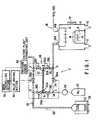
- FIG. 1shows a process gas supply apparatus 2 according to an embodiment of the present invention.
- the process gas supply apparatus 2is connected to a process chamber 6, thereby constituting main section of a semiconductor manufacturing apparatus.
- the process chamber 2houses a object to be processed (hereinafter, referred to as a "substrate W") such as a semiconductor wafer or an LCD substrate.
- a substrate Wa object to be processed
- TiCl 4 (titanium tetrachloride gas) gasis supplied as a process gas from the process gas supply apparatus 2 to the process chamber 6, thereby forming a Ti film on the substrate W set in the process chamber 6.
- the process chamber 6is formed of, for example, aluminium and the inner surface thereof is coated with aluminum oxide.
- the process chamber 6has a mounting table (susceptor) 8 therein for mounting the substrate W.
- the mounting table 8houses a heating means, such as a resistance heater 10, for heating the substrate W mounted on the mounting table 8 to a predetermined temperature and maintaining it at the predetermined temperature.
- An exhaust port 12is formed through the bottom of the process chamber 6 to set the inner pressure of the process chamber 6 at a predetermined vacuum level.
- the exhaust port 12is connected to a vacuum pump system (not shown).
- a gate valve 14is attached onto the side wall of the process chamber 6. The substrate W is loaded into and out from the process chamber 6 through the gate valve 14.
- a shower head 16is attached for introducing the gas to be supplied to the process chamber 6 uniformly into the process chamber 6.
- the shower head 16has two gas supply port 16A, 16B.
- One (16B) of the two gas supply portis connected to a gas supply system 18 for supplying a reaction gas such as an NH 3 (ammonia) gas required for film formation.
- the other gas supply port 16Ais connected to the process gas supply apparatus 2.
- the process gas supply apparatus 2has not only a N 2 gas source 20 filled with N 2 gas (serving as a carrier gas) but also a TiCl 4 gas source 22 for supplying a TiCl 4 gas (serving as a process gas).
- the N 2 gas source 20is connected to the gas supply port 16A of the shower head 16 by way of a carrier gas path (pipe) 24.
- a regulator 26 for sending out the N 2 gas stored in the N 2 gas source 20 at a predetermined pressureis attached to a portion of the carrier gas path 24 positioned in the proximity of the gas exhaust port of the N 2 gas source 20.
- An end of a gas exhaust path (pipe) 30is connected to the TiCl 4 gas source 22 and the other end of the gas exhaust path 30 is connected to an exhaust duct of a factory plant (not shown) which is set at about atmospheric pressure.
- a temperature controlling mechanism 28such as a heater is positioned in the periphery of the TiCl 4 gas source 22.
- the temperature controlling mechanism 28heats liquid-state TiCl 4 (TiCl 4 is present in the form of a liquid at room temperature) stored in the TiCl 4 gas source 22 at a predetermined temperature, thereby generating the TiCl 4 gas. In this way, the TiCl 4 gas is sent out from the TiCl 4 gas source 22 at a predetermined pressure.
- the carrier gas path 24is connected to the gas exhaust path 30 via two auxiliary tubes 34, 36.
- the auxiliary tubes 34 and 36are connected to each other by a measuring tube (gas storing section) 32 whose volume is set at a predetermined value.
- Flanges 32A, 32Aare respectively provided at both ends of the measuring tube 32. These flanges 32A, 32A are connected airtight by means of fixing means such as bolts, to flanges 34A, 36A which are respectively provided at the auxiliary tubes 34, 36.
- a valve mechanism 38consisting of a plurality of valves is provided on the path 24, 30 and the auxiliary tubes 34, 36.
- the valve mechanism 38consists of a first valve 38A attached in the middle of the carrier gas path 24, a second valve 38B attached in the middle of the gas exhaust path 30, third and fourth valves 38C, 38D attached in the middle of the auxiliary tube 34, and fifth and sixth valves 38E, 38F attached in the middle of the auxiliary tube 36.
- the first valve 38Ais located between a junction C which connects the auxiliary tube 34 to the carrier gas path 24 and a junction D which connects the auxiliary tube 36 to the carrier gas path 24.
- the second valve 38Bis located between a junction E which connects the auxiliary tube 34 to the gas exhaust path 30 and a junction F which connects the auxiliary tube 36 to the gas exhaust path 30.
- the third and fourth valves 38C, 38Dare respectively located at both sides of a junction A which connects the measuring tube 32 to the auxiliary tube 34.
- the fifth and sixth valves 38E, 38Fare respectively located at both sides of a junction B which connects the measuring tube 32 and the auxiliary tube 36.
- the third and fourth valves 38C and 38Dare arranged near the junction A and the fifth and sixth valves 38E and 38F are arranged near the junction B.
- the open/shut control of each of valves 38A-38Fis effected by a valve driving section 40 controlled by a main controlling section 70 of the semiconductor manufacturing device.
- the measuring tube 32 to be detachably connected between the auxiliary tube 34 and 36has a predetermined volume (small volume) which is previously set by defining the inner diameter and the length accurately.
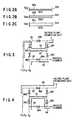
- Various type of measuring tubes 32a-32c different in volumeare shown in FIGs. 2A-2C. Volumes of the measuring tubes 32a, 32b, 32c connected between the auxiliary tubes 34 and 36 are set so as to give total volumes of 10CC, 30CC, and 50CC, respectively.
- the tube volume of the auxiliary tube 34 between the valves 38C and 38D and the tube volume of the auxiliary tube 36 between the valves 38E and 38Fmust be included in the total volume used herein.
- these measuring tubes different in volumeare selectively used depending upon the amount of the process gas required at the film formation time.
- a heater 50(indicated by a broken line) such as a tape heater is attached to the TiCl 4 gas flowing portions of paths 24, 30 and the auxiliary tubes 34, 36.
- the heater 40plays a role in preventing the TiCl 4 gas from condensing to be converted into a liquid in the middle of the paths 24, 30 and the auxiliary tubes 34, 36.
- the six valves 38A to 38Fare set in a discrete form in this embodiment, the entire structure may be simplified significantly if use is made of a multiple valve unit having six valves 38A to 38F incorporated therein.
- the N 2 gasis used as a carrier gas herein, however, other inert gas such as an Ar gas and a He gas may be used.
- the tube volume of the measuring tube 32is not limited to 10cc , 30cc , and 50cc.
- the inner diameter of the measuring tube 32 and those of the auxiliary tubes 34, 36may be substantially equal.
- the measuring tube 32capable of supplying a flow amount corresponding upon a desired film thickness is installed between the auxiliary tubes 34 and 36 of the process gas supply apparatus 2.
- the measuring tube 32a shown in FIG. 2Ais installed between the auxiliary tubes 34 and 36.
- the substrate Wis mounted on the mounting table 8 in the process chamber 6 and heated to a predetermined temperature.
- the process chamber 6is vacuumed to set at a predetermined process pressure.
- the process temperatureis set at 600°C
- the process pressureis set within the range of 10 m Torr to 10 Torr (for example, about 300 m Torr).
- a NH 3 gas serving as a reaction gasis supplied in a predetermined amount from the gas supply system 18 into the process chamber 6.
- the first, fourth and sixth valves, 38A, 38D, 38Fare opened, whereas the second, third and fifth valves, 38B, 38C, 38E are closed.
- the N 2 gas (serving as a carrier gas) supplied from the N 2 gas source 20is controlled by the regulator 26 always at a constant pressure and directly introduced into the process chamber 6 by way of the carrier gas path 24, as indicated by an arrow 42 in FIG. 3.
- the TiCl 4 gas (serving as a process gas) supplied from the TiCl 4 gas source 22is controlled by the temperature controlling mechanism 22 always at a constant pressure, and introduced into the measuring tube 32 by way of the gas exhaust path 30 and the fourth valve 38D, as indicated by an arrow 44 in FIG. 3.
- the TiCl 4 gasis exhausted toward the exhaust duct of a factory plant by way of the sixth valve 38F and the gas exhaust path 30.
- the measuring tube 32is always filled with a certain amount (i.e., 10cc) of the TiCl 4 gas.
- the pressure of both paths 24 and 30are controlled substantially equal.
- the TiCl 4 gasis generated by heating a liquid-state TiCl 4 to about 75°C by the temperature controlling mechanism 22.
- the heater 40heats each passage to about 80°C to prevent the TiCl 4 gas from condensing to be converted into a liquid.
- the first, fourth, and sixth valves 38A, 38D, 38Fare switched to closed positions; at the same time, the second, third, and fifth valves 38B, 38C, 38E are switched to open positions. All these switching operations are carried out simultaneously.
- the N 2 gas (serving as a carrier gas) supplied form the N 2 gas supply source 20is introduced into the measuring tube 32 by way of the carrier gas path 24 and the third valve 38C and then flows into the process chamber 6 by way of the fifth valve 38E and the carrier gas path 24, as indicated by an arrow 46 in FIG. 4.
- the TiCl 4 gas stored in the measuring tube 32is pushed by the carrier gas and flows into the process chamber 6.
- the TiCl 4 gas supplied from the gas source 22is directly exhausted to the exhaust duct of the factory plant by way of the gas exhaust path 30 without passing through the measuring tube 32, as indicated by an arrow 48 in FIG. 4.
- a pressure sensor 60for detecting the inner pressure of the measuring tube 32 may be arranged in order to confirm that the measuring tube 32 is completely filled with the TiCl 4 gas.
- the detection signalis sent to the main controlling section 70.
- the main controlling section 70switches the first, fourth and sixth valves 38A, 38D, 38F to closed positions; at the same time, the second, third, and fifth valves 38B, 38C, 38E to open positions.
- the third and fifth valves 38C, 38Emay be constructed as a relief valve and these valves 38C, 38F may be opened at the time the measuring tube 32 is completely filled with the TiCl 4 gas.
- the gas exhaust path 30is allowed to communicate with the measuring tube 32 by means of the valve mechanism 38, thereby filling the measuring tube 32 with a constant amount of the process gas.
- the measuring tube 32is allowed to communicate with the carrier gas path 24 by means of the valve mechanism 38.
- the process gas stored in the measuring tube 32is pushed by the carrier gas and supplied into the process chamber 6.
- the process gascan be supplied into the process chamber 6 accurately in a predetermined amount defined by the volume of the measuring tube 32.
- the filmis accurately formed on the substrate W in a predetermined thickness which is defined by the gas supply amount.
- the thickness of the film to be formedcan be controlled accurately.
- the flow amount of the process gas to be suppliedis controlled accurately by using the corresponding measuring tube, the thickness of the film to be formed can be controlled accurately.
- the flow amountcan be minutely controlled, with the result that very thin film can be formed accurately. Such a minute control cannot be attained by a conventionally-used mass-controller.
- the inner pressures of the both paths 24, 30are always controlled substantially equal. Therefore, pressure of the process chamber 6 does not change at the switchover time of the valves 38A to 38F. It is therefore possible to control the film thickness accurately without change in process conditions.
- switchover operations of the valves 38A-38Fare effected simultaneously.
- the switchover operationis not limited to the method of the aforementioned embodiment.
- the open-close state shown in FIG. 3may be changed into that shown in FIG. 4 as follows: the fourth and sixth valves 38D, 38F are closed and the second valve 38B is opened, thereby isolating the TiCl 4 gas stored in the measuring tube 32 temporality. Thereafter, the third and fifth valves 38C, 38E are opened, at the same time, the first valve 38A is closed.
- the measuring tube 32b of 30cc shown in FIG. 2Bmay be used.
- the valve switchover operationmay be repeated intermittently three times by using the measuring tube 32a of 10cc shown in FIG. 2A, thereby supplying 30cc of TiCl 4 gas to the process chamber 6, in total.
- the TiCl 4 gascan be supplied in a requisite flow amount as a whole.
- the filmis formed by supplying the gas intermittently a plurality of times, it is considered that the film is stayed in the equivalent state as an annealing while the film formation gas is not supplied. As a result, the resistance of the film becomes low, improving the quality of the film.
- This apparatusincludes a plurality of gas storing portions 52, 53, 54.
- the process gascan be selectively filled into or released from one or two or more of the gas storing portions, in a desired amount.
- the gas storing portions 52, 53, 54are different in content and individually connected to a carrier gas pipe 24 and a process gas pipe 30 by way of the open/shut means 58 discretely provided.
- the controlling section 70controls the open/shut means 58 in the same manner as in the aforementioned embodiment, thereby filling the process gas into the gas storing portion(s) 52, 53, 54 arbitrarily chosen and sending the process gas therefrom to the process chamber 6.
- gas storing portions 52, 53, 54are defined as 10, 20, 30cc and if the gas storing portions are appropriately chosen alone or in combination, gas can be introduced into the process chamber accurately in an amount of 10, 20, 30, 40, 50, or 60cc.
- NH 3 (ammonia) gasis supplied. If the gas supply system 18 is formed in the same construction as that of the process-gas supply apparatus 2, the NH 3 gas-flow, even in a small amount, can be controlled accurately.
- a Ti filmis formed on the substrate W.
- a process gas sourcecapable of generating a process gas required for the formation of the desired film, can be connected to the gas exhaust path 30 in place of the TiCl 4 gas source 22.
- the process gas supply apparatus 2 of this embodimentis not necessary to be used in a single-processing semiconductor manufacturing apparatus and may be used in a batch-type semiconductor manufacturing apparatus capable of processing a plurality of substrates simultaneously.
- a glass substrate and an LCD substrate other than the semiconductor wafermay be mentioned.
Landscapes
- Chemical & Material Sciences (AREA)
- General Chemical & Material Sciences (AREA)
- Chemical Kinetics & Catalysis (AREA)
- Engineering & Computer Science (AREA)
- Materials Engineering (AREA)
- Mechanical Engineering (AREA)
- Metallurgy (AREA)
- Organic Chemistry (AREA)
- Chemical Vapour Deposition (AREA)
- Physical Vapour Deposition (AREA)
- Electrodes Of Semiconductors (AREA)
Description
- The present invention relates to a process gassupply apparatus and method for supplying a process gas into aprocess chamber arranged in a process apparatus such asa semiconductor manufacturing apparatus and having aobject to be processed set therein,and relates to a film forming apparatus whichincludes such process gas supply apparatus.
- Generally, in a manufacturing process of asemiconductor integrated circuit, a film formationprocess, pattern etching, and the like, are repeatedlyapplied onto a semiconductor wafer or a glass substrate,thereby obtaining a desired device. Recently, linewidth and gate width have become narrow associated witha tendency toward miniaturization and high integrationof the semiconductor integrated circuit. Also, thefilm thickness tends to be reduced since the semiconductorintegrated circuit is increasingly desired tohave a multilevel interconnection structure.
- As mentioned above, when the thickness of theformed film is reduced as a result of the highintegration and the multi-layer tendency of theintegrated circuit, it becomes critical to control aflow amount of a process gas accurately for forming afilm. To control the flow amount accurately, a flow-amountcontroller such as a mass-flow controller isgenerally used in the semiconductor manufacturingapparatus. However, the mass-controller is notsuitable for controlling a small amount of a gas flow for the reason of its structural characteristics.In fact, it is difficult to accurately form a gateelectrode and wiring of several hundreds of angstromsin thickness under the control by the mass-flowcontroller.
- Document JP-A-03-141192 discloses a process gas supplyapparatus for feeding a gas stored in the storage chamberinto a reactor while being controlled by a valve. The flowamount of the gas is controlled by the valve. Therefore, thisprior art apparatus is not suitable for controlling a smallamount of a gas flow.
- Document EP-A2-0 307 995 discloses a process and a device forgas delivery to an epitaxy apparatus, that is a pulsedreactor. For preparing a gas mixture which can be regulatedvery accurately in respect of quantity and composition, andthe composition of which can be changed very rapidly withoutlosses, each of the gases of the gas mixture is fed to aseparate gas pipette and thereafter the content of the gaspipette is passed cyclically, by a pressure differential,into the pulsed reactor, with the composition of the mixturebeing changed per one or more cycles.
- An object of the present invention is to providea process gas supply apparatus and method capable of supplyinga small amount of the process gas accurately bycontrolling the flow amount.
- The object of the present invention can beachieved by a process gas supply apparatus for and methodaccording to claim 1 and claim 13, respectively.
- Preferred embodiments of the invention are indicatedin the dependent claims.
- This invention can be more fully understood fromthe following detailed description when taken inconjunction with the accompanying drawings, in which:
- FIG. 1 is a circuit diagram of a circuitconstitution of a process gas supply apparatusaccording to an embodiment of the present invention;
- FIG. 2A is a schematic view of a measuring tubeof 10CC;
- FIG. 2B is a schematic view of a measuring tubeof 30CC;
- FIG. 2C is a schematic view of a measuring tubeof 50CC;
- FIG. 3 is a diagram showing a gas-flow route inthe process gas supply apparatus of FIG. 1;
- FIG. 4 is a diagram showing another gas flow routein the process gas supply apparatus of FIG. 1; and
- FIG. 5 is a circuit diagram showing anothercircuit constitution.
- Hereinbelow, an embodiment of the presentinvention will be explained with reference to theaccompanying drawings.
- FIG. 1 shows a process
gas supply apparatus 2 according to an embodiment of the present invention.The processgas supply apparatus 2 is connected to aprocess chamber 6, thereby constituting main section ofa semiconductor manufacturing apparatus. Theprocesschamber 2 houses a object to be processed (hereinafter,referred to as a "substrate W") such as a semiconductorwafer or an LCD substrate. In the semiconductormanufacturing apparatus of this embodiment, TiCl4(titanium tetrachloride gas) gas is supplied as aprocess gas from the processgas supply apparatus 2 tothe process chamber 6, thereby forming a Ti film on thesubstrate W set in the process chamber 6. - The process chamber 6 is formed of, for example,aluminium and the inner surface thereof is coatedwith aluminum oxide. The process chamber 6 has amounting table (susceptor) 8 therein for mounting thesubstrate W. The mounting table 8 houses a heatingmeans, such as a
resistance heater 10, for heating thesubstrate W mounted on the mounting table 8 to apredetermined temperature and maintaining it at thepredetermined temperature. An exhaust port 12 isformed through the bottom of the process chamber 6 toset the inner pressure of the process chamber 6 at apredetermined vacuum level. The exhaust port 12 isconnected to a vacuum pump system (not shown). A gatevalve 14 is attached onto the side wall of the processchamber 6. The substrate W is loaded into and out fromthe process chamber 6 through the gate valve 14. - In the ceiling section of the process chamber 6,a
shower head 16 is attached for introducing the gasto be supplied to the process chamber 6 uniformlyinto the process chamber 6. Theshower head 16 hastwogas supply port 16A, 16B. One (16B) of the twogas supply port is connected to agas supply system 18for supplying a reaction gas such as an NH3 (ammonia)gas required for film formation. The othergas supplyport 16A is connected to the processgas supply apparatus 2. - The process
gas supply apparatus 2 has not only aN2 gas source 20 filled with N2 gas (serving as acarrier gas) but also a TiCl4 gas source 22 forsupplying a TiCl4 gas (serving as a process gas).The N2 gas source 20 is connected to thegas supplyport 16A of theshower head 16 by way of a carrier gaspath (pipe) 24. Aregulator 26 for sending out the N2gas stored in the N2 gas source 20 at a predeterminedpressure is attached to a portion of thecarrier gaspath 24 positioned in the proximity of the gas exhaustport of the N2 gas source 20. An end of a gas exhaustpath (pipe) 30 is connected to the TiCl4 gas source 22and the other end of thegas exhaust path 30 isconnected to an exhaust duct of a factory plant(not shown) which is set at about atmospheric pressure.A temperature controllingmechanism 28 such as a heateris positioned in the periphery of the TiCl4 gassource 22. The temperature controllingmechanism 28heats liquid-state TiCl4 (TiCl4 is present in theform of a liquid at room temperature) stored in theTiCl4 gas source 22 at a predetermined temperature,thereby generating the TiCl4 gas. In this way, theTiCl4 gas is sent out from the TiCl4 gas source 22 ata predetermined pressure. - The
carrier gas path 24 is connected to thegas exhaust path 30 via twoauxiliary tubes auxiliary tubes Flanges measuring tube 32. Theseflanges flanges auxiliary tubes - To control communication of the
measuring tube 32with thecarrier gas path 24 and thegas exhaust path 30, avalve mechanism 38 consisting of a pluralityof valves is provided on thepath auxiliary tubes valve mechanism 38consists of afirst valve 38A attached in the middle ofthecarrier gas path 24, asecond valve 38B attached inthe middle of thegas exhaust path 30, third andfourthvalves auxiliarytube 34, and fifth andsixth valves auxiliary tube 36. In this case,thefirst valve 38A is located between a junction Cwhich connects theauxiliary tube 34 to thecarrier gaspath 24 and a junction D which connects theauxiliarytube 36 to thecarrier gas path 24. Thesecond valve 38B is located between a junction E which connects theauxiliary tube 34 to thegas exhaust path 30 and ajunction F which connects theauxiliary tube 36 to thegas exhaust path 30. - The third and
fourth valves measuring tube 32 to theauxiliarytube 34. The fifth andsixth valves measuring tube 32 and theauxiliarytube 36. To reduce the tube volume of theauxiliarytube 34 located between thevalves auxiliary tube 36 locatedbetween thevalves fourth valves sixth valves valves 38A-38F is effected by avalve driving section 40 controlled by a maincontrollingsection 70 of the semiconductormanufacturing device. - The
measuring tube 32 to be detachably connectedbetween theauxiliary tube tubes 32a, 32b, 32c connected between theauxiliary tubes auxiliary tube 34 between thevalves auxiliary tube 36between thevalves - Note that a heater 50 (indicated by a broken line)such as a tape heater is attached to the TiCl4 gasflowing portions of
paths auxiliarytubes heater 40 plays a role in preventingthe TiCl4 gas from condensing to be converted into aliquid in the middle of thepaths auxiliary tubes valves 38A to38F are set in a discrete form in this embodiment, theentire structure may be simplified significantly if useis made of a multiple valve unit having sixvalves 38Ato 38F incorporated therein. The N2 gas is used as acarrier gas herein, however, other inert gas such as anAr gas and a He gas may be used. The tube volume ofthe measuringtube 32 is not limited to 10cc , 30cc ,and 50cc. The inner diameter of the measuringtube 32and those of theauxiliary tubes - Now, we will explain the case in which a Ti filmis formed on the substrate W in the process chamber 6by making use of the process
gas supply apparatus 2constructed in the above. - When the TiCl4 gas is supplied at a constantpressure, it has been empirically known how thick thefilm is formed depending upon the flow amount. Prior to the initiating the film formation process, themeasuring
tube 32 capable of supplying a flow amountcorresponding upon a desired film thickness isinstalled between theauxiliary tubes gas supply apparatus 2. For example, providedthat 10cc of the TiCl4 gas in flow amount is requiredfor forming the Ti film in a desired thickness of 100Åunder a constant pressure, the measuring tube 32a shownin FIG. 2A is installed between theauxiliary tubes - After the measuring
tube 32 having a predeterminedvolume (hereinafter, the volume is regarded as 10cc)is set between theauxiliary tubes gassupply system 18 into the process chamber 6. - In this step (the step before the film formationis initiated), the first, fourth and sixth valves, 38A,38D, 38F are opened, whereas the second, third andfifth valves, 38B, 38C, 38E are closed. Hence, the N2gas (serving as a carrier gas) supplied from the N2 gassource 20 is controlled by the
regulator 26 always ata constant pressure and directly introduced into theprocess chamber 6 by way of thecarrier gas path 24,as indicated by anarrow 42 in FIG. 3. The TiCl4 gas(serving as a process gas) supplied from the TiCl4 gassource 22 is controlled by thetemperature controllingmechanism 22 always at a constant pressure, andintroduced into the measuringtube 32 by way of thegasexhaust path 30 and thefourth valve 38D, as indicated by anarrow 44 in FIG. 3. Then, the TiCl4 gas isexhausted toward the exhaust duct of a factory plant byway of thesixth valve 38F and thegas exhaust path 30.When the TiCl4 gas flows through the route mentioned,the measuringtube 32 is always filled with a certainamount (i.e., 10cc) of the TiCl4 gas. - In the process
gas supply apparatus 2, thepressure of bothpaths temperature controlling mechanism 22. Theheater 40heats each passage to about 80°C to prevent the TiCl4gas from condensing to be converted into a liquid. - After the gas flows as shown in FIG. 3 and themeasuring
tube 32 is filled with 10cc of TiCl4 gas, thefirst, fourth, andsixth valves fifth valves gas supply source 20 is introduced into the measuringtube 32 by way of thecarrier gas path 24 and thethirdvalve 38C and then flows into the process chamber 6 byway of thefifth valve 38E and thecarrier gas path 24,as indicated by anarrow 46 in FIG. 4. At this time,the TiCl4 gas stored in the measuringtube 32 is pushedby the carrier gas and flows into the process chamber 6.Whereas, the TiCl4 gas supplied from thegas source 22is directly exhausted to the exhaust duct of thefactory plant by way of thegas exhaust path 30 withoutpassing through the measuringtube 32, as indicated byanarrow 48 in FIG. 4. - In the process
gas supply apparatus 2 of thisembodiment, a pressure sensor 60 (as shown in FIG. 1)for detecting the inner pressure of the measuringtube 32 may be arranged in order to confirm that the measuringtube 32 is completely filled with the TiCl4gas. In this case, upon detecting that the measuringtube 32 is completely filled with TiCl4 gas by thepressure sensor 60, the detection signal is sent to themain controllingsection 70. Themain controllingsection 70 switches the first, fourth andsixth valves fifth valves fifthvalves valves tube 32 is completely filled with theTiCl4 gas. - As explained in the foregoing, in the process
gassupply apparatus 2 of this embodiment, thegas exhaustpath 30 is allowed to communicate with the measuringtube 32 by means of thevalve mechanism 38, therebyfilling the measuringtube 32 with a constant amount ofthe process gas. Thereafter, the measuringtube 32 isallowed to communicate with thecarrier gas path 24 bymeans of thevalve mechanism 38. As a result, theprocess gas stored in the measuringtube 32 is pushedby the carrier gas and supplied into the processchamber 6. In this way, the process gas can besupplied into the process chamber 6 accurately in apredetermined amount defined by the volume of themeasuringtube 32. As a result, the film is accuratelyformed on the substrate W in a predetermined thicknesswhich is defined by the gas supply amount. - If the flow amount of the process gas to besupplied is controlled accurately by using thecorresponding measuring tube, the thickness of thefilm to be formed can be controlled accurately. Inparticular, if a small volume measuring tube is used,the flow amount can be minutely controlled, with theresult that very thin film can be formed accurately.Such a minute control cannot be attained by a conventionally-used mass-controller.
- In the process
gas supply apparatus 2 of thisembodiment, the inner pressures of the bothpaths valves 38A to 38F.It is therefore possible to control the film thicknessaccurately without change in process conditions. - In the aforementioned embodiment, switchoveroperations of the
valves 38A-38F are effectedsimultaneously. However, as long as the TiCl4 gasstored in the measuringtube 32 is transported intothe process chamber 6 without failure, the switchoveroperation is not limited to the method of theaforementioned embodiment. For example, the open-closestate shown in FIG. 3 may be changed into that shown inFIG. 4 as follows: the fourth andsixth valves second valve 38B is opened,thereby isolating the TiCl4 gas stored in the measuringtube 32 temporality. Thereafter, the third andfifthvalves firstvalve 38A is closed. - In the aforementioned embodiment, when 30cc of theTiCl4 gas is required in order to form a film in adesired thickness, the measuring
tube 32b of 30cc shownin FIG. 2B may be used. Alternatively, the valveswitchover operation may be repeated intermittentlythree times by using the measuring tube 32a of 10ccshown in FIG. 2A, thereby supplying 30cc of TiCl4 gasto the process chamber 6, in total. In brief,according to the constitution of the aforementionedembodiment, in the case where the switchover operationis repeated intermittently appropriate times, the TiCl4gas can be supplied in a requisite flow amount as awhole. In the case where the film is formed bysupplying the gas intermittently a plurality of times,it is considered that the film is stayed in the equivalent state as an annealing while the filmformation gas is not supplied. As a result, theresistance of the film becomes low, improving thequality of the film. - In another case where a plurality of measuring
tubes 32 are connected in parallel and placed betweenthe junctions A and B, the same effects can be obtained.Such a constitution is shown in FIG. 5. This apparatusincludes a plurality ofgas storing portions gas storingportions carrier gas pipe 24 and aprocess gas pipe 30 by way of the open/shut means 58discretely provided. - The controlling
section 70 controls the open/shutmeans 58 in the same manner as in the aforementionedembodiment, thereby filling the process gas into thegas storing portion(s) 52, 53, 54 arbitrarily chosenand sending the process gas therefrom to the processchamber 6. - If the contents of
gas storing portions - In the aforementioned embodiment, NH3 (ammonia)gas is supplied. If the
gas supply system 18 is formedin the same construction as that of the process-gassupply apparatus 2, the NH3 gas-flow, even in a smallamount, can be controlled accurately. In theembodiment, a Ti film is formed on the substrate W.When a TiN film or a TiSi film is desired to be formed onthe substrate W, a process gas source capable ofgenerating a process gas required for the formation of the desired film, can be connected to thegas exhaustpath 30 in place of the TiCl4 gas source 22.
The processgas supply apparatus 2 of this embodimentis not necessary to be used in a single-processingsemiconductor manufacturing apparatus and may be usedin a batch-type semiconductor manufacturing apparatuscapable of processing a plurality of substratessimultaneously. As examples of the substrate W tobe processed in the processgas supply apparatus 2of the embodiment, a glass substrate and an LCDsubstrate other than the semiconductor wafer may bementioned.
Claims (14)
- A process gas supply apparatus (2) comprising:wherein the process gas releasing pipe (30), the firstauxiliary tube (34), the second auxiliary tube (36), themeasuring tube (32), and the carrier gas introducingpipe (24) form a circuit, for filling the process gaswhich flows through the process gas releasing pipe (30)into the measuring tube (32) to the predetermined volumeby communicating the process gas releasing pipe (30)with the measuring tube (32), and releasing the processgas filled in the measuring tube (32) toward the processchamber (6) under guidance of the carrier gas thereafterby communicating the carrier gas introducing pipe (24)with the measuring tube (32).a) a process gas source (22) for supplying a processgas to a process chamber (6) in which apredetermined processing using the process gas isapplied to an object (W) placed therein;b) a carrier gas source (20) filled with a carriergas;c) a process gas releasing pipe (30) having one endconnected to the process gas source (22), forsupplying the process gas;d) a carrier gas introducing pipe (24) having one endconnected to the carrier gas source (20) andanother end connected to the process chamber (6),for supplying the carrier gas;e) a first auxiliary tube (34) having one endconnected to the process gas releasing pipe (30)and another end connected to the carrier gasintroducing pipe (24);f) a second auxiliary tube (36) having one endconnected to the process gas releasing pipe (30)and another end connected to the carrier gasintroducing pipe (24);g) at least one measuring tube (32) set to have apredetermined volume and having one end connectedto the first auxiliary tube (34) and another endconnected to the second auxiliary tube (36);h) a valve mechanism (38) comprising a plurality ofvalves respectively provided on the process gasreleasing pipe (30), the first auxiliary tube (34),the second auxiliary tube (36), and the carrier gasintroducing pipe (24), for controlling acommunication state between the process gasreleasing pipe (30), the first auxiliary tube (34),the second auxiliary tube (36), the measuring tube(32), and the carrier gas introducing pipe (24);andi) a controlling section (70) for controlling theopen/shut states of the plurality of valves,
- The process gas supply apparatus (2) according to claim1, wherein the valve mechanism (38) comprises
a first valve (38A) provided in a middle of the carriergas introducing pipe (24),
a second valve (38B) provided in a middle of the processgas releasing pipe (30),
a third valve (38C) and a fourth valve (38D) provided ina middle of the first auxiliary tube (34), and
a fifth valve (38E) and a sixth valve (38F) provided ina middle of the second auxiliary tube (36),
the first valve (38A) is located between a junction (C)which connects the carrier gas introducing pipe (24) tothe first auxiliary tube (34) and a junction (D) whichconnects the carrier gas introducing pipe (24) to thesecond auxiliary tube (36),
the second valve (38B) is located between a junction (E)which connects the process gas releasing pipe (30) tothe first auxiliary tube (34) and a junction (F) whichconnects the process gas releasing pipe (30) to thesecond auxiliary tube (36),
the third valve (38C) and the fourth valve (38D) arerespectively located adjacent to both sides of ajunction (A), which connects the first auxiliary tube(34) to the measuring tube (32) and is located betweenthe junctions (C and E), which are respectively locatedat the ends of the first auxiliary tube (34), and
the fifth valve (38E) and sixth valve (38F) arerespectively located adjacent to both sides of ajunction (B), which connects the second auxiliary tube(36) to the measuring tube (32) and is located betweenthe junctions (D and F), which are respectively locatedat the ends of the second auxiliary tube (36). - The process gas supply apparatus (2) according to claim2, wherein the circuit comprises a process gas fillingcircuit and a process gas releasing circuit,
the process gas filling circuit fills the process gas,which flows through the process gas releasing pipe (30),into the measuring tube (32) to the predeterminedvolume, by shutting the second valve (38B), the thirdvalve (38C), and the fifth valve (38E), whilesimultaneously opening the fourth valve (38D) and thesixth valve (38F) for communicating the process gasreleasing pipe (30) with the measuring tube (32) andshutting the fourth valve (38D) and the sixth valve(38F) thereafter, and
the process gas releasing circuit introduces the carriergas, which flows through the carrier gas introducingpipe, into the measuring tube (32) by shutting the firstvalve (38A), the fourth valve (38D), and the sixth valve(38F), while simultaneously opening the third valve(38C) and the fifth valve (38E) for communicating thecarrier gas introducing pipe (24) with the measuringtube (32) toward the process chamber (6), under guidanceof the carrier gas. - The process gas supply apparatus (2) according to claim1, wherein the measuring tube (32) can be attached tothe first auxiliary tube (34) and the second auxiliarytube (36) in a detachable manner.
- The process gas supply apparatus (2) according to claim2, wherein the third valve (38C) and the fifth valve(38E) are relief valves, and said relief valves areopened when the measuring tube (32) is filled with theprocess gas to the predetermined volume.
- The process gas supply apparatus (2) according to claim2, wherein each of the valves constituting the valvemechanism (38) comprises a multiple valve unit.
- The process gas supply apparatus (2) according to claim1, wherein the process gas releasing pipe (30) isconnected to an exhaust duct.
- The process gas supply apparatus (2) according to claim1, further comprising a detection sensor (60) fordetecting an inner pressure of the measuring tube (32),wherein
the controlling section (70) controls a switchover ofthe open/shut state of each of the valves, whichconstitute the valve mechanism (38), based on detectioninformation from the detection sensor (60). - The process gas supply apparatus (2) according to claim1, wherein an inner pressure of the process gasreleasing pipe (30) is set substantially equal to aninner pressure of the carrier gas introducing pipe (24).
- The process gas supply apparatus (2) according to claim1, wherein the measuring tube (32) has a volume requiredfor forming a film having a predetermined thickness onthe object (W).
- The process gas supply apparatus (2) according to claim1, wherein inner diameters of pipe routes (24, 30, 32,34, 36), which constitute the process-gas fillingcircuit, are set substantially equal to one another.
- The process gas supply apparatus (2) according to claim1, wherein the measuring tube (32) is provided with aheater (50) for preventing the process gas from beingcondensed and liquefied.
- A process gas supply method comprising the steps of:wherein a predetermined amount of the process gasis supplied to the process chamber (6) byintermittently repeating the method steps a) to c)for a plurality of times.a) filling a predetermined volume of a process gasinto at least one measuring tube (32) having saidpredetermined volume;b) introducing a carrier gas from one end of themeasuring tube (32) into the measuring tube (32)filled with the predetermined volume of processgas; andc) releasing the predetermined volume of process gastogether with the carrier gas from another end ofthe measuring tube (32) toward a process chamber(6);
- A film forming apparatus comprising:a process chamber (6) in which a predeterminedprocessing using a process gas is applied to an object(W) placed therein; andthe process gas supply apparatus (2) according to one ofclaims 1 to 12.
Applications Claiming Priority (3)
| Application Number | Priority Date | Filing Date | Title |
|---|---|---|---|
| JP130261/97 | 1997-05-02 | ||
| JP9130261AJPH10306377A (en) | 1997-05-02 | 1997-05-02 | Method for supplying minute amount of gas and device therefor |
| JP13026197 | 1997-05-02 |
Publications (2)
| Publication Number | Publication Date |
|---|---|
| EP0875595A1 EP0875595A1 (en) | 1998-11-04 |
| EP0875595B1true EP0875595B1 (en) | 2004-09-15 |
Family
ID=15030046
Family Applications (1)
| Application Number | Title | Priority Date | Filing Date |
|---|---|---|---|
| EP98107948AExpired - LifetimeEP0875595B1 (en) | 1997-05-02 | 1998-04-30 | Process-gas supply apparatus |
Country Status (4)
| Country | Link |
|---|---|
| US (1) | US5989345A (en) |
| EP (1) | EP0875595B1 (en) |
| JP (1) | JPH10306377A (en) |
| DE (1) | DE69826171T2 (en) |
Families Citing this family (59)
| Publication number | Priority date | Publication date | Assignee | Title |
|---|---|---|---|---|
| US6749717B1 (en)* | 1997-02-04 | 2004-06-15 | Micron Technology, Inc. | Device for in-situ cleaning of an inductively-coupled plasma chambers |
| JP2000124195A (en)* | 1998-10-14 | 2000-04-28 | Tokyo Electron Ltd | Surface treatment method and device |
| US6217659B1 (en)* | 1998-10-16 | 2001-04-17 | Air Products And Chemical, Inc. | Dynamic blending gas delivery system and method |
| US7732327B2 (en) | 2000-06-28 | 2010-06-08 | Applied Materials, Inc. | Vapor deposition of tungsten materials |
| US7964505B2 (en) | 2005-01-19 | 2011-06-21 | Applied Materials, Inc. | Atomic layer deposition of tungsten materials |
| US7405158B2 (en) | 2000-06-28 | 2008-07-29 | Applied Materials, Inc. | Methods for depositing tungsten layers employing atomic layer deposition techniques |
| FR2812665B1 (en)* | 2000-08-01 | 2003-08-08 | Sidel Sa | PLASMA COATING DEPOSITION METHOD, DEVICE FOR IMPLEMENTING THE METHOD AND COATING OBTAINED BY SUCH A PROCESS |
| US6451692B1 (en)* | 2000-08-18 | 2002-09-17 | Micron Technology, Inc. | Preheating of chemical vapor deposition precursors |
| US6878206B2 (en) | 2001-07-16 | 2005-04-12 | Applied Materials, Inc. | Lid assembly for a processing system to facilitate sequential deposition techniques |
| US6561220B2 (en)* | 2001-04-23 | 2003-05-13 | International Business Machines, Corp. | Apparatus and method for increasing throughput in fluid processing |
| US7211144B2 (en) | 2001-07-13 | 2007-05-01 | Applied Materials, Inc. | Pulsed nucleation deposition of tungsten layers |
| TW581822B (en) | 2001-07-16 | 2004-04-01 | Applied Materials Inc | Formation of composite tungsten films |
| US20030029715A1 (en) | 2001-07-25 | 2003-02-13 | Applied Materials, Inc. | An Apparatus For Annealing Substrates In Physical Vapor Deposition Systems |
| US7081271B2 (en) | 2001-12-07 | 2006-07-25 | Applied Materials, Inc. | Cyclical deposition of refractory metal silicon nitride |
| JP4071968B2 (en)* | 2002-01-17 | 2008-04-02 | 東芝三菱電機産業システム株式会社 | Gas supply system and gas supply method |
| US6833161B2 (en) | 2002-02-26 | 2004-12-21 | Applied Materials, Inc. | Cyclical deposition of tungsten nitride for metal oxide gate electrode |
| US6972267B2 (en) | 2002-03-04 | 2005-12-06 | Applied Materials, Inc. | Sequential deposition of tantalum nitride using a tantalum-containing precursor and a nitrogen-containing precursor |
| US7279432B2 (en) | 2002-04-16 | 2007-10-09 | Applied Materials, Inc. | System and method for forming an integrated barrier layer |
| JP4217870B2 (en)* | 2002-07-15 | 2009-02-04 | 日本電気株式会社 | Organosiloxane copolymer film, manufacturing method thereof, growth apparatus, and semiconductor device using the copolymer film |
| JP4352783B2 (en)* | 2002-08-23 | 2009-10-28 | 東京エレクトロン株式会社 | Gas supply system and processing system |
| US6936086B2 (en)* | 2002-09-11 | 2005-08-30 | Planar Systems, Inc. | High conductivity particle filter |
| EP1420080A3 (en) | 2002-11-14 | 2005-11-09 | Applied Materials, Inc. | Apparatus and method for hybrid chemical deposition processes |
| US7169231B2 (en)* | 2002-12-13 | 2007-01-30 | Lam Research Corporation | Gas distribution system with tuning gas |
| JP4180948B2 (en)* | 2003-03-24 | 2008-11-12 | 東京エレクトロン株式会社 | Substrate processing apparatus, substrate processing method, and gas nozzle |
| US7211508B2 (en) | 2003-06-18 | 2007-05-01 | Applied Materials, Inc. | Atomic layer deposition of tantalum based barrier materials |
| US9725805B2 (en)* | 2003-06-27 | 2017-08-08 | Spts Technologies Limited | Apparatus and method for controlled application of reactive vapors to produce thin films and coatings |
| US7638167B2 (en)* | 2004-06-04 | 2009-12-29 | Applied Microstructures, Inc. | Controlled deposition of silicon-containing coatings adhered by an oxide layer |
| US20050271893A1 (en)* | 2004-06-04 | 2005-12-08 | Applied Microstructures, Inc. | Controlled vapor deposition of multilayered coatings adhered by an oxide layer |
| US20040261703A1 (en)* | 2003-06-27 | 2004-12-30 | Jeffrey D. Chinn | Apparatus and method for controlled application of reactive vapors to produce thin films and coatings |
| KR100514170B1 (en)* | 2003-07-25 | 2005-09-09 | 삼성전자주식회사 | Apparatus for forming thin film and method for forming thin film using the same |
| US7727588B2 (en)* | 2003-09-05 | 2010-06-01 | Yield Engineering Systems, Inc. | Apparatus for the efficient coating of substrates |
| KR100541814B1 (en)* | 2003-09-15 | 2006-01-11 | 삼성전자주식회사 | Chemical Vapor Deposition Equipment |
| KR100589053B1 (en)* | 2003-10-15 | 2006-06-12 | 삼성전자주식회사 | Source supply device, source supply method and atomic layer deposition method using the same |
| KR20050040969A (en)* | 2003-10-29 | 2005-05-04 | 삼성전자주식회사 | Diffusion system |
| US20050252449A1 (en) | 2004-05-12 | 2005-11-17 | Nguyen Son T | Control of gas flow and delivery to suppress the formation of particles in an MOCVD/ALD system |
| US7879396B2 (en)* | 2004-06-04 | 2011-02-01 | Applied Microstructures, Inc. | High aspect ratio performance coatings for biological microfluidics |
| WO2006020424A2 (en)* | 2004-08-02 | 2006-02-23 | Veeco Instruments Inc. | Multi-gas distribution injector for chemical vapor deposition reactors |
| JP5264039B2 (en)* | 2004-08-10 | 2013-08-14 | 東京エレクトロン株式会社 | Thin film forming apparatus and thin film forming method |
| JP5043684B2 (en)* | 2005-01-27 | 2012-10-10 | アプライド マテリアルズ インコーポレイテッド | Ruthenium layer deposition apparatus and method |
| US20070271751A1 (en)* | 2005-01-27 | 2007-11-29 | Weidman Timothy W | Method of forming a reliable electrochemical capacitor |
| US20060201425A1 (en)* | 2005-03-08 | 2006-09-14 | Applied Microstructures, Inc. | Precursor preparation for controlled deposition coatings |
| JP4506677B2 (en)* | 2005-03-11 | 2010-07-21 | 東京エレクトロン株式会社 | Film forming method, film forming apparatus, and storage medium |
| TWI332532B (en) | 2005-11-04 | 2010-11-01 | Applied Materials Inc | Apparatus and process for plasma-enhanced atomic layer deposition |
| US8088248B2 (en)* | 2006-01-11 | 2012-01-03 | Lam Research Corporation | Gas switching section including valves having different flow coefficients for gas distribution system |
| EP2006414A2 (en)* | 2006-03-30 | 2008-12-24 | Mitsui Engineering & Shipbuilding Co., Ltd. | Atomic layer growing apparatus |
| US7521379B2 (en) | 2006-10-09 | 2009-04-21 | Applied Materials, Inc. | Deposition and densification process for titanium nitride barrier layers |
| US8821637B2 (en) | 2007-01-29 | 2014-09-02 | Applied Materials, Inc. | Temperature controlled lid assembly for tungsten nitride deposition |
| US8900695B2 (en) | 2007-02-23 | 2014-12-02 | Applied Microstructures, Inc. | Durable conformal wear-resistant carbon-doped metal oxide-comprising coating |
| US20080248263A1 (en)* | 2007-04-02 | 2008-10-09 | Applied Microstructures, Inc. | Method of creating super-hydrophobic and-or super-hydrophilic surfaces on substrates, and articles created thereby |
| US8236379B2 (en)* | 2007-04-02 | 2012-08-07 | Applied Microstructures, Inc. | Articles with super-hydrophobic and-or super-hydrophilic surfaces and method of formation |
| US20100062149A1 (en) | 2008-09-08 | 2010-03-11 | Applied Materials, Inc. | Method for tuning a deposition rate during an atomic layer deposition process |
| US8491967B2 (en) | 2008-09-08 | 2013-07-23 | Applied Materials, Inc. | In-situ chamber treatment and deposition process |
| JP5854668B2 (en)* | 2011-07-07 | 2016-02-09 | 芝浦メカトロニクス株式会社 | Gas-liquid mixed fluid generating apparatus, gas-liquid mixed fluid generating method, processing apparatus, and processing method |
| CN104707494A (en)* | 2015-03-30 | 2015-06-17 | 上海纳诺巴伯纳米科技有限公司 | Preparation device and preparation method for over-saturated hydrogen solution |
| DE102016003875A1 (en)* | 2016-03-31 | 2017-10-05 | Linde Aktiengesellschaft | Volumetric and gravimetric level for the production of gas mixtures |
| JP6763274B2 (en)* | 2016-10-14 | 2020-09-30 | 東京エレクトロン株式会社 | Film forming equipment, cleaning method of film forming equipment and storage medium |
| US11393703B2 (en) | 2018-06-18 | 2022-07-19 | Applied Materials, Inc. | Apparatus and method for controlling a flow process material to a deposition chamber |
| TW202200830A (en)* | 2020-02-26 | 2022-01-01 | 美商應用材料股份有限公司 | Sequential pulse and purge for ald processes |
| JP7675366B2 (en)* | 2021-07-09 | 2025-05-13 | 日本エア・リキード合同会社 | Sublimation gas supply system and sublimation gas supply method |
Family Cites Families (8)
| Publication number | Priority date | Publication date | Assignee | Title |
|---|---|---|---|---|
| NL8702096A (en)* | 1987-09-04 | 1989-04-03 | Stichting Katholieke Univ | METHOD AND APPARATUS FOR MIXING GASES AND EPITACTICALLY MANUFACTURING SEMICONDUCTOR PRODUCTS USING A GAS MIXTURE |
| JPH03141192A (en)* | 1989-10-26 | 1991-06-17 | Fujitsu Ltd | Vapor phase growth apparatus and vapor phase growth method |
| JP3207943B2 (en)* | 1992-11-17 | 2001-09-10 | 忠弘 大見 | Low temperature oxide film forming apparatus and low temperature oxide film forming method |
| JPH06330323A (en)* | 1993-05-18 | 1994-11-29 | Mitsubishi Electric Corp | Semiconductor device manufacturing apparatus and cleaning method thereof |
| US5616208A (en)* | 1993-09-17 | 1997-04-01 | Tokyo Electron Limited | Vacuum processing apparatus, vacuum processing method, and method for cleaning the vacuum processing apparatus |
| US5777300A (en)* | 1993-11-19 | 1998-07-07 | Tokyo Electron Kabushiki Kaisha | Processing furnace for oxidizing objects |
| US5575854A (en)* | 1993-12-30 | 1996-11-19 | Tokyo Electron Limited | Semiconductor treatment apparatus |
| US5620524A (en)* | 1995-02-27 | 1997-04-15 | Fan; Chiko | Apparatus for fluid delivery in chemical vapor deposition systems |
- 1997
- 1997-05-02JPJP9130261Apatent/JPH10306377A/enactivePending
- 1998
- 1998-04-30EPEP98107948Apatent/EP0875595B1/ennot_activeExpired - Lifetime
- 1998-04-30DEDE69826171Tpatent/DE69826171T2/ennot_activeExpired - Fee Related
- 1998-04-30USUS09/069,987patent/US5989345A/ennot_activeExpired - Lifetime
Also Published As
| Publication number | Publication date |
|---|---|
| DE69826171D1 (en) | 2004-10-21 |
| JPH10306377A (en) | 1998-11-17 |
| EP0875595A1 (en) | 1998-11-04 |
| DE69826171T2 (en) | 2005-11-17 |
| US5989345A (en) | 1999-11-23 |
Similar Documents
| Publication | Publication Date | Title |
|---|---|---|
| EP0875595B1 (en) | Process-gas supply apparatus | |
| US6905549B2 (en) | Vertical type semiconductor device producing apparatus | |
| KR100282853B1 (en) | Apparatus for thin film deposition using cyclic gas injection | |
| US7860597B2 (en) | Atomic layer deposition apparatus | |
| US5782980A (en) | Low pressure chemical vapor deposition apparatus including a process gas heating subsystem | |
| KR101015985B1 (en) | Substrate processing apparatus | |
| KR101210456B1 (en) | Method of manufacturing semiconductor device, method of processing substrate and substrate processing apparatus | |
| JP4235076B2 (en) | Semiconductor manufacturing apparatus and semiconductor manufacturing method | |
| KR20210128914A (en) | Raw material supply apparatus and film forming apparatus | |
| JP2564482B2 (en) | Deposition film forming equipment | |
| JP4903619B2 (en) | Substrate processing equipment | |
| JP2010212335A (en) | Substrate-treating device | |
| US7211514B2 (en) | Heat-processing method for semiconductor process under a vacuum pressure | |
| WO2020246309A1 (en) | Substrate processing method and substrate processing device | |
| US20030140857A1 (en) | Apparatus and method for low pressure CVD deposition of tungsten and tungsten nitride | |
| JP4941514B2 (en) | Process gas supply apparatus and film forming apparatus | |
| US11107704B2 (en) | Gas input system for a substrate processing chamber | |
| JP4509697B2 (en) | Substrate processing equipment | |
| JP2597245B2 (en) | Exhaust system for CVD system | |
| JPH09143739A (en) | Method for supplying treating gas and device therefor | |
| JP2011061002A (en) | Substrate processing apparatus | |
| JPH0623566Y2 (en) | Semiconductor manufacturing equipment | |
| CN115773471A (en) | Atomic layer deposition apparatus and method thereof | |
| JPH0663095B2 (en) | CVD equipment | |
| JP2005197541A (en) | Substrate processing equipment |
Legal Events
| Date | Code | Title | Description |
|---|---|---|---|
| PUAI | Public reference made under article 153(3) epc to a published international application that has entered the european phase | Free format text:ORIGINAL CODE: 0009012 | |
| 17P | Request for examination filed | Effective date:19980430 | |
| AK | Designated contracting states | Kind code of ref document:A1 Designated state(s):DE FR GB | |
| AX | Request for extension of the european patent | Free format text:AL;LT;LV;MK;RO;SI | |
| AKX | Designation fees paid | Free format text:DE FR GB | |
| 17Q | First examination report despatched | Effective date:20000110 | |
| GRAP | Despatch of communication of intention to grant a patent | Free format text:ORIGINAL CODE: EPIDOSNIGR1 | |
| GRAS | Grant fee paid | Free format text:ORIGINAL CODE: EPIDOSNIGR3 | |
| GRAA | (expected) grant | Free format text:ORIGINAL CODE: 0009210 | |
| AK | Designated contracting states | Kind code of ref document:B1 Designated state(s):DE FR GB | |
| REG | Reference to a national code | Ref country code:GB Ref legal event code:FG4D | |
| REF | Corresponds to: | Ref document number:69826171 Country of ref document:DE Date of ref document:20041021 Kind code of ref document:P | |
| ET | Fr: translation filed | ||
| PLBE | No opposition filed within time limit | Free format text:ORIGINAL CODE: 0009261 | |
| STAA | Information on the status of an ep patent application or granted ep patent | Free format text:STATUS: NO OPPOSITION FILED WITHIN TIME LIMIT | |
| 26N | No opposition filed | Effective date:20050616 | |
| PGFP | Annual fee paid to national office [announced via postgrant information from national office to epo] | Ref country code:GB Payment date:20070425 Year of fee payment:10 | |
| PGFP | Annual fee paid to national office [announced via postgrant information from national office to epo] | Ref country code:FR Payment date:20070411 Year of fee payment:10 | |
| PGFP | Annual fee paid to national office [announced via postgrant information from national office to epo] | Ref country code:DE Payment date:20080508 Year of fee payment:11 | |
| GBPC | Gb: european patent ceased through non-payment of renewal fee | Effective date:20080430 | |
| REG | Reference to a national code | Ref country code:FR Ref legal event code:ST Effective date:20081231 | |
| PG25 | Lapsed in a contracting state [announced via postgrant information from national office to epo] | Ref country code:FR Free format text:LAPSE BECAUSE OF NON-PAYMENT OF DUE FEES Effective date:20080430 | |
| PG25 | Lapsed in a contracting state [announced via postgrant information from national office to epo] | Ref country code:GB Free format text:LAPSE BECAUSE OF NON-PAYMENT OF DUE FEES Effective date:20080430 | |
| PG25 | Lapsed in a contracting state [announced via postgrant information from national office to epo] | Ref country code:DE Free format text:LAPSE BECAUSE OF NON-PAYMENT OF DUE FEES Effective date:20091103 |