EP0871227A2 - Thin film transistor, manufacturing method therefor and liquid crystal display unit using the same - Google Patents
Thin film transistor, manufacturing method therefor and liquid crystal display unit using the sameDownload PDFInfo
- Publication number
- EP0871227A2 EP0871227A2EP98106371AEP98106371AEP0871227A2EP 0871227 A2EP0871227 A2EP 0871227A2EP 98106371 AEP98106371 AEP 98106371AEP 98106371 AEP98106371 AEP 98106371AEP 0871227 A2EP0871227 A2EP 0871227A2
- Authority
- EP
- European Patent Office
- Prior art keywords
- thin film
- polycrystalline silicon
- implanted
- region
- impurity
- Prior art date
- Legal status (The legal status is an assumption and is not a legal conclusion. Google has not performed a legal analysis and makes no representation as to the accuracy of the status listed.)
- Granted
Links
Images


Classifications
- H—ELECTRICITY
- H10—SEMICONDUCTOR DEVICES; ELECTRIC SOLID-STATE DEVICES NOT OTHERWISE PROVIDED FOR
- H10D—INORGANIC ELECTRIC SEMICONDUCTOR DEVICES
- H10D86/00—Integrated devices formed in or on insulating or conducting substrates, e.g. formed in silicon-on-insulator [SOI] substrates or on stainless steel or glass substrates
- H10D86/01—Manufacture or treatment
- H10D86/021—Manufacture or treatment of multiple TFTs
- H10D86/0221—Manufacture or treatment of multiple TFTs comprising manufacture, treatment or patterning of TFT semiconductor bodies
- H—ELECTRICITY
- H10—SEMICONDUCTOR DEVICES; ELECTRIC SOLID-STATE DEVICES NOT OTHERWISE PROVIDED FOR
- H10D—INORGANIC ELECTRIC SEMICONDUCTOR DEVICES
- H10D30/00—Field-effect transistors [FET]
- H10D30/60—Insulated-gate field-effect transistors [IGFET]
- H10D30/67—Thin-film transistors [TFT]
- H10D30/6729—Thin-film transistors [TFT] characterised by the electrodes
- H10D30/673—Thin-film transistors [TFT] characterised by the electrodes characterised by the shapes, relative sizes or dispositions of the gate electrodes
- H10D30/6733—Multi-gate TFTs
- G—PHYSICS
- G02—OPTICS
- G02F—OPTICAL DEVICES OR ARRANGEMENTS FOR THE CONTROL OF LIGHT BY MODIFICATION OF THE OPTICAL PROPERTIES OF THE MEDIA OF THE ELEMENTS INVOLVED THEREIN; NON-LINEAR OPTICS; FREQUENCY-CHANGING OF LIGHT; OPTICAL LOGIC ELEMENTS; OPTICAL ANALOGUE/DIGITAL CONVERTERS
- G02F1/00—Devices or arrangements for the control of the intensity, colour, phase, polarisation or direction of light arriving from an independent light source, e.g. switching, gating or modulating; Non-linear optics
- G02F1/01—Devices or arrangements for the control of the intensity, colour, phase, polarisation or direction of light arriving from an independent light source, e.g. switching, gating or modulating; Non-linear optics for the control of the intensity, phase, polarisation or colour
- G02F1/13—Devices or arrangements for the control of the intensity, colour, phase, polarisation or direction of light arriving from an independent light source, e.g. switching, gating or modulating; Non-linear optics for the control of the intensity, phase, polarisation or colour based on liquid crystals, e.g. single liquid crystal display cells
- G02F1/133—Constructional arrangements; Operation of liquid crystal cells; Circuit arrangements
- G02F1/1333—Constructional arrangements; Manufacturing methods
- G02F1/1345—Conductors connecting electrodes to cell terminals
- G02F1/13454—Drivers integrated on the active matrix substrate
- H—ELECTRICITY
- H10—SEMICONDUCTOR DEVICES; ELECTRIC SOLID-STATE DEVICES NOT OTHERWISE PROVIDED FOR
- H10D—INORGANIC ELECTRIC SEMICONDUCTOR DEVICES
- H10D30/00—Field-effect transistors [FET]
- H10D30/01—Manufacture or treatment
- H10D30/021—Manufacture or treatment of FETs having insulated gates [IGFET]
- H10D30/031—Manufacture or treatment of FETs having insulated gates [IGFET] of thin-film transistors [TFT]
- H10D30/0312—Manufacture or treatment of FETs having insulated gates [IGFET] of thin-film transistors [TFT] characterised by the gate electrodes
- H10D30/0314—Manufacture or treatment of FETs having insulated gates [IGFET] of thin-film transistors [TFT] characterised by the gate electrodes of lateral top-gate TFTs comprising only a single gate
- H—ELECTRICITY
- H10—SEMICONDUCTOR DEVICES; ELECTRIC SOLID-STATE DEVICES NOT OTHERWISE PROVIDED FOR
- H10D—INORGANIC ELECTRIC SEMICONDUCTOR DEVICES
- H10D30/00—Field-effect transistors [FET]
- H10D30/01—Manufacture or treatment
- H10D30/021—Manufacture or treatment of FETs having insulated gates [IGFET]
- H10D30/031—Manufacture or treatment of FETs having insulated gates [IGFET] of thin-film transistors [TFT]
- H10D30/0321—Manufacture or treatment of FETs having insulated gates [IGFET] of thin-film transistors [TFT] comprising silicon, e.g. amorphous silicon or polysilicon
- H—ELECTRICITY
- H10—SEMICONDUCTOR DEVICES; ELECTRIC SOLID-STATE DEVICES NOT OTHERWISE PROVIDED FOR
- H10D—INORGANIC ELECTRIC SEMICONDUCTOR DEVICES
- H10D30/00—Field-effect transistors [FET]
- H10D30/60—Insulated-gate field-effect transistors [IGFET]
- H10D30/67—Thin-film transistors [TFT]
- H10D30/6704—Thin-film transistors [TFT] having supplementary regions or layers in the thin films or in the insulated bulk substrates for controlling properties of the device
- H10D30/6713—Thin-film transistors [TFT] having supplementary regions or layers in the thin films or in the insulated bulk substrates for controlling properties of the device characterised by the properties of the source or drain regions, e.g. compositions or sectional shapes
- H10D30/6715—Thin-film transistors [TFT] having supplementary regions or layers in the thin films or in the insulated bulk substrates for controlling properties of the device characterised by the properties of the source or drain regions, e.g. compositions or sectional shapes characterised by the doping profiles, e.g. having lightly-doped source or drain extensions
- H—ELECTRICITY
- H10—SEMICONDUCTOR DEVICES; ELECTRIC SOLID-STATE DEVICES NOT OTHERWISE PROVIDED FOR
- H10D—INORGANIC ELECTRIC SEMICONDUCTOR DEVICES
- H10D30/00—Field-effect transistors [FET]
- H10D30/60—Insulated-gate field-effect transistors [IGFET]
- H10D30/67—Thin-film transistors [TFT]
- H10D30/6729—Thin-film transistors [TFT] characterised by the electrodes
- H10D30/6737—Thin-film transistors [TFT] characterised by the electrodes characterised by the electrode materials
- H10D30/6739—Conductor-insulator-semiconductor electrodes
- H—ELECTRICITY
- H10—SEMICONDUCTOR DEVICES; ELECTRIC SOLID-STATE DEVICES NOT OTHERWISE PROVIDED FOR
- H10D—INORGANIC ELECTRIC SEMICONDUCTOR DEVICES
- H10D86/00—Integrated devices formed in or on insulating or conducting substrates, e.g. formed in silicon-on-insulator [SOI] substrates or on stainless steel or glass substrates
- H10D86/40—Integrated devices formed in or on insulating or conducting substrates, e.g. formed in silicon-on-insulator [SOI] substrates or on stainless steel or glass substrates characterised by multiple TFTs
- H10D86/60—Integrated devices formed in or on insulating or conducting substrates, e.g. formed in silicon-on-insulator [SOI] substrates or on stainless steel or glass substrates characterised by multiple TFTs wherein the TFTs are in active matrices
Definitions
- the present inventionrelates to an Lightly-Doped-Drain structure (hereinafter, abbreviated to LDD structure) for the purpose of reducing leakage current in a polycrystalline silicon thin-film transistor (hereinafter, abbreviated to TFT) and a manufacturing method therefor, whose technique is applicable to a liquid crystal display unit or the like.
- LDD structureLightly-Doped-Drain structure
- TFTpolycrystalline silicon thin-film transistor
- the LDD structureis proposed.
- a structure in which LDD structures are connected in seriesis also proposed. A description on this technique is found, for example, in International Display Research Conference '93, p. 465.
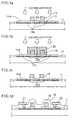
- FIGS. 5a to 5dshow a method for manufacturing a conventional TFT in which LDD structures are connected in series.
- an amorphous silicon thin-filmis formed on a light-transmittal glass substrate 11 (highly heat-resistant glass substrate) by the plasma chemical vapor deposition (PCVD) method and is subjected to thermal treatment at 600°C to form a polycrystalline silicon thin-film 13 serving as an active layer.
- PCVDplasma chemical vapor deposition
- This polycrystalline silicon thin-filmis machined into the shape of isles and a silicon oxide thin-film serving as a gate insulating film 14a is formed thereon in a thickness of 85 nm.
- a silicon oxide thin-filmserving as a gate insulating film 14a is formed thereon in a thickness of 85 nm.
- two gate electrodes 15are formed on this silicon oxide thin-film.
- a first impurityis implanted with the gate electrodes 15 employed as masks by the ion plantation method to form an implanted region (n- region) 13b of the lower-concentration impurity.
- phosphorus (P) ionsare implanted under an acceleration voltage of 80 kV in a dose amount of 1 x 10 13 /cm 2 .
- the polycrystalline silicon thin-film below the gate electrodes 15serves as the channel region 13a of the TFT.
- an implantation mask using a photoresistis formed on the LDD region of the TFT with the aid of a photoresist 25 as shown in FIG. 5b and then a second impurity is implanted to form an implanted region (n+ region) 13c of the higher-concentration impurity serving as the source and drain regions of the TFT.
- an openingis provided also on the polycrystalline silicon region between the gate electrodes and the resist mask is formed in such a shape that the thin polycrystalline silicon films between the electrodes of each gates are connected via both of the implanted region 13b of the lower-concentration impurity and the implanted region 13c of the higher-concentration impurity.
- phosphorus (P) ionsare implanted under an acceleration voltage of 80 kV in a dose amount of 1 x 10 15 /cm 2 .
- the photoresist maskis removed and the activation treatment of the implanted impurity is given at 900°C for 2 hours.
- an inter-layer insulating film 16is formed as shown in FIG. 5c.
- source and drain electrodes 21 and 22are formed after boring the respective contact holes, and a TFT is completed.
- the TFT explained in the conventional examplehas the implanted region 13c of the higher-concentration impurity equal in concentration to the source and drain regions between the electrodes of each gates. For this reason, an opening needs to be formed in the doping mask at the forming time of the source and drain regions of the TFTs connected in series, i.e., photoresist 25, as shown in FIG. 5b.
- the length of the implanted region 13b of the lower-concentration impurity between the electrodes of each gatesis restricted by the value given by adding the mask focusing accuracy of the exposer to the design size.
- Wa ( ⁇ m), Ld ( ⁇ m) and La ( ⁇ m)be the minimum exposure width of the exposer in a TFT having a series-connected construction of TFTs having the LDD structure, the design length of the lower-concentration impurity implanted region, and the focusing accuracy of the exposer, respectively, it is difficult to make the minimum size of each TFT not greater than Wa + 2Ld + La .
- a case of employing such an element as the switching element of a liquid crystal display unitcauses a reduction in the opening ratio of the liquid crystal display unit, thus posing problems such as a lowering in luminosity or an increase in consumed power.
- TFTs having an LDD structureit is an object of the present invention to provide a TFT capable of making the element minute while reducing the leakage current of the TFT, a manufacturing method therefor, and a liquid crystal display unit.
- the present inventionprovides a TFT having a polycrystalline silicon thin film employed as an active layer and a plurality of gate electrodes provided in one TFT, wherein low-concentration impurity implanted regions are provided between a channel region and source and drain regions of the TFT, and polycrystalline silicon thin films between each gate electrodes are connected only by low-concentration impurity implanted regions.
- the present inventionprovides a TFT having a polycrystalline silicon thin film employed as the active layer, a gate insulating film provided on the polycrystalline silicon thin film, and a plurality of gate electrodes provided on the gate insulating film, wherein in forming an LDD structure with low-concentration impurity implanted regions provided between the channel region and the source and drain regions, the first impurity is implanted with the gate electrode employed as a mask, thereafter an implantation mask is formed on a region serving as the LDD region including the polycrystalline silicon region between gate electrodes, and thus a second impurity is implanted.
- the present inventionprovides a TFT having a polycrystalline silicon thin film employed as the active layer, a gate insulating film provided on the polycrystalline silicon thin film, and a plurality of gate electrodes provided on the gate insulating film, wherein in forming an LDD structure with implanted regions of a low-concentration impurity between the channel region and the source and drain regions, a single-time implantation of an impurity is carried out with the gate electrodes employed as mask after stacking a foreign insulating film on the polycrystalline silicon thin film, the upper layer insulating film of the above gate insulating film is removed at least on the source and drain regions, and the insulating film is machined into such a shape as to cover the low-concentration impurity region and the polycrystalline silicon between each gate electrodes.
- the present inventionprovides an active matrix array for a liquid crystal display unit with a polycrystalline silicon thin film employed as the active layer and a drive circuit integrated in one same substrate, comprising a plurality of gate electrodes at least for a TFT for driving pixel electrodes, and an LDD structure with implanted regions of a low-concentration impurity between the channel region and the source and drain regions of the above TFT, wherein the polycrystalline silicon thin film between each gate electrodes is connected by the implanted region of a low-concentration impurity.
- the TFT of the present inventionrelates to a TFT having a polycrystalline silicon thin-film employed as the active layer, and a plurality of gate electrodes provided in one transistor, characterized in that implanted polycrystalline sylicon regions between a channel region and source and drain regions of the TFT are implanted with an impurity at a lower concentration than the above source and drain regions, and the polycrystalline silicon thin-films between each gate electrodes are formed only of the above implanted polycrystalline silicon thin-films implanted with an impurity at a lower concentration.
- the size between each gate electrodescan be defined only by the minimum line width of an exposer, and both reduction in element size and decrease in leakage current can be realized.
- the TFT according to the present inventionis featured by the sheet resistance of an implanted polycrystalline silicon thin-film implanted with an impurity at a low concentration being preferably 5 k ⁇ - 150 k ⁇ .
- the TFT according to the present inventionis featured by the total length of all the polycrystalline silicon thin-films implanted with a low-concentration impurity included between the source and drain regions ranging from 6 ⁇ m to 12 ⁇ m in the longitudinal direction of the channel of the TFT.
- a method for manufacturing the TFT according to the present inventionis featured by comprising the steps of: after implanting the first impurity, forming an implantation mask on regions serving as the LDD region including the region above the polycrystalline silicon region between the gate electrodes; and by implanting a second impurity, forming an implanted region of a high-concentration impurity serving as the source and drain regions of the TFT.
- the method for manufacturing the TFT according to the present inventionis featured by comprising the steps of: stacking a foreign gate insulating film on the polycrystalline silicon thin-film; removing the upper layer insulating film of the above gate insulating film at least on the source and drain regions; machining said insulating film in such a shape as to cover the low-concentration impurity region and the polycrystalline silicon film between each gate electrodes; thereafter forming the source and drain regions of the TFT and the implanted region of a low-concentration impurity by a single-time implantation of the impurity; and after implanting the impurity, removing an upper layer gate insulating film covering the low
- a liquid crystal display unit using an active matrix array according to the present inventionis featured in that the active matrix array having a polycrystalline silicon thin film employed as the active layer and a drive circuit integrated in one same substrate comprises: a plurality of gate electrodes at least for a TFT for driving the pixel electrodes; an LDD structure with implanted regions of a low-concentration impurity between the channel region and the source and drain regions of the above TFT; and the polycrystalline silicon thin film between the electrodes of each gates which is formed only of an implanted region of a low-concentration impurity.
- FIGS. 1a to 1dare sectional views of TFTs according to Embodiment 1 of the present invention.
- FIGS. 2a to 2dare sectional views of TFTs according to Embodiment 2 of the present invention.
- FIGS. 3a to 3dare sectional views of active matrix arrays for a liquid crystal display unit according to Embodiment 3 of the present invention.
- FIG. 4is a sectional view of the liquid crystal display unit using the active matrix array according to Embodiment 3 of the present invention.
- FIGS. 5a to 5dare sectional views of conventional TFTs.
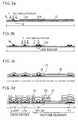
- FIGS. 1a to 1dshow the manufacturing steps of a TFT with the LDD structure of Embodiment 1 of the present invention.
- an amorphous silicon thin filmis formed on a glass substrate 11 surface-coated with silicon oxide in a thickness of 50 nm by the plasma CVD method.
- the amorphous silicon thin filmAfter being subjected to heat treatment in nitrogen under 450°C for 90 minutes to reduce the hydrogen concentration in the film, the amorphous silicon thin film is crystallized by the excimer laser irradiation to form a polycrystalline silicon thin film 13 serving as the active layer.
- This polycrystalline silicon thin film 13is machined into the shape of a TFT, and a silicon oxide film is formed thereon in a thickness of 85 nm to serve as a gate insulating film 14a.
- the gate electrode 15On this silicon oxide film, two gate electrodes 15 connected electrically are formed. Each inter-electrode distance is formed to be a minimum line width of 5 ⁇ m of the exposer.
- the gate electrode 15comprises an 80 nm thick titanium (Ti) so formed as to come into contact with the silicon oxide film, and a 100 nm aluminum (Al) alloy containing 7.4 % of zirconium (Zr) on the titanium film in a total thickness of 180 nm.
- a first impurity implantationis carried out for implanting phosphorus (P) at an acceleration voltage of 80 kV in an implantation dose amount of 1 x 10 13 /cm 2 with the gate electrode 15 employed as a mask by the ion doping method so as to form an implanted region (n- region) 13b of the lower-concentration impurity.
- a gas mixture of hydrogen gas and PH 3 of 5 % concentrationis subjected to plasma decomposition by high-frequency discharge, and the generated ions are implanted into a TFT without a mass separation process.
- the polycrystalline silicon thin film below the gate electrode 15serves as the channel region 13a of the TFT.
- an implantation maskis formed on the LDD region of the TFT by using a photoresist 25 as described in FIG. 1b and thereafter a second impurity is implanted to form an implanted region (n+ region) 13c of the higher-concentration impurity serving as the source and drain regions of the TFT.
- a second impurityis implanted to form an implanted region (n+ region) 13c of the higher-concentration impurity serving as the source and drain regions of the TFT.
- phosphorus (P) ionsare implanted at an acceleration voltage of 80 kV in a dose amount of 1 x 10 15 /cm 2 .
- the resist maskis so formed as to completely cover the top of the polycrystalline silicon region between each gate electrodes.
- the polycrystalline silicon thin film between each gate electrodesis formed in such a shape as to be connected only through the implanted region 13b of the lower-concentration impurity.
- the photoresist maskis removed as shown in FIG. 1c to perform an activation treatment of the implanted impurity.
- an inter-layer insulating film 16is formed as shown in FIG. 1d.
- the source and drain electrodes 21 and 22are formed, thus completing a TFT.
- FIGS. 2a to 2dshow the manufacturing steps of a TFT having the LDD structure of Embodiment 2 of the present invention.
- an amorphous silicon thin filmis formed on a glass substrate 11 surface-coated with silicon oxide in a thickness of 50 nm by the plasma CVD method. After being subjected to heat treatment in nitrogen under 450°C for 90 minutes to reduce the hydrogen concentration in the film, the amorphous silicon film is crystallized by the excimer laser annealing to form a thin polycrystalline silicon film 13 serving as the active layer.
- This polycrystalline silicon thin film 13is machined into the shape of a TFT to form thereon a silicon oxide film serving as the gate insulating film 14a in a thickness of 85 nm.
- a tantalum oxide film serving as a second gate insulating film 14bis formed in a thickness of 50 nm.
- two gate electrodes 15are formed on the tantalum oxide film.
- the gate electrode 15comprises an 80 nm thick titanium (Ti) so formed as to come into contact with the tantalum oxide film and a 100 nm aluminum (Al) alloy containing 7.4 % of zirconium (Zr) on the titanium film in a total thickness of 180 nm.
- the dual gate electrodeAfter the formation of the dual gate electrode, only the region above the LDD regions and between both electrodes of the TFT is coated with tantalum oxide, and the tantalum oxide films above the source and drain regions are selectively removed.
- phosphorus (P)is implanted at an acceleration voltage of 80 kV in an implantation dose amount of 1 x 10 15 /cm 2 by the ion doping method as shown in FIG. 2b.
- a gas mixture of hydrogen gas and PH 3 of 5 % concentrationis subjected to plasma decomposition by high-frequency discharge and the generated ions are implanted into a TFT without a mass separation process.
- phosphorus ionsare implanted through the monolayer silicon oxide film in the source and drain regions of the TFT, and through the laminate film of tantalum oxide and silicon oxide in the LDD regions and the region between each gate electrodes.
- the implantation amountdecreases as compared with the regions implanted through the monolayer silicon oxide film, i.e., the source and drain regions of the TFT.
- both of the source and drain regions corresponding to the implanted region 13c of the higher-concentration impurity and the LDD regions corresponding to the implanted region 13b of the lower-concentration impurityare formed simultaneously.
- each gate electrodes of the TFTare connected by the implanted region 13b of the low-concentration impurity comprising a polycrystalline silicon thin film implanted with the low-concentration impurity of the same concentration as with the LDD regions.
- the polycrystalline silicon thin films below the gate electrodes 15serve as the channel region 13a of the TFT.
- the tantalum oxide thin filmis removed on the LDD regions as shown in FIG. 2c.
- the inter-layer insulating film 16 made of silicon oxideis formed as shown in FIG. 2d. Silicon oxide is formed at 430°C by the normal pressure CVD method, and the impurity implanted simultaneously in this process can be activated. Finally, after boring a contact hole, the source and drain electrodes 21 and 22 are formed, thus completing a TFT.
- FIGS. 3a to 3dshow the manufacturing steps of an active matrix array for a liquid crystal display unit according to Embodiment 3 of the present invention.
- an amorphous silicon thin filmis formed on a glass substrate 11 surface-coated with silicon oxide in a thickness of 50 nm by the plasma CVD method. After being subjected to heat treatment in nitrogen under 450°C for 90 minutes to reduce the hydrogen concentration in the film, the amorphous silicon film is crystallized by the excimer laser annealing to form a polycrystalline silicon thin film 13.
- the polycrystalline silicon thin film 13is machined into the shape of a TFT to form a silicon oxide film serving as the gate insulating film 14a in a thickness of 85 nm.
- a tantalum oxide film serving as a second gate insulating film 14bis formed in a thickness of 50 nm.
- gate electrodes 15are formed on a p-channel TFT.
- the gate electrode 15comprises an 80 nm thick titanium (Ti) film so formed as to come into contact with the tantalum oxide film and a 150 nm aluminum (Al) alloy film containing 7.4 % of zirconium (Zr) on the titanium film in a total thickness of 230 nm.
- a gate electrode materialis coated on the n-channel TFT.
- boron (B)is implanted into the source and drain regions of the p-channel TFT. Boron implantation proceeds at an acceleration voltage of 60 kV in a dose amount of 5 x 10 15 /cm 2 by using the ion doping method.
- a gate electrode 15is formed on the n-channel TFT as shown in FIG. 3b.
- the gate electrode of a pixel TFTis of a dual gate construction, and the tantalum oxide films above the source and drain regions are selectively removed with the tantalum oxide films above the LDD region and between each gate electrodes of the pixel TFT being left as they are.
- phosphorus (P)is implanted at an acceleration voltage of 80 kV in an implantation dose amount of 1 x 10 15 /cm 2 by the ion doping method.
- each gate electrodes of a pixel TFTare connected by the polycrystalline silicon thin film into which a low-concentration impurity identical in concentration to that in the LDD regions is implanted.
- the thin tantalum oxide films above the LDD regions and between each gate electrodesare removed using the gate electrodes as a mask. This tantalum oxide removal process enables the OFF current of the TFT to be greatly reduced.
- a first inter-layer insulating film 16 comprising silicon oxideis formed.
- the silicon oxideis formed at 430°C by using the normal pressure CVD method, and the impurity implanted simultaneously in this process can be activated.
- a pixel electrode 18 comprising an ITO (Indium-Tin-Oxide) filmis formed, and a second inter-layer insulating layer 17 comprising silicon oxide is formed.
- the source and drain electrodes 21 and 22are formed as shown in FIG. 3d. Further, after a silicon nitride film serving as the protective film 23 is formed by the plasma CVD and subjected to a 350°C annealing in the atmosphere of hydrogen, the silicon nitride and silicon oxide laminate films above the pixel electrode 18 are selectively removed to complete an active matrix array.
- FIG. 4is one example of a sectional constitution view of a liquid crystal display unit fabricated by using an active matrix array shown in FIGS. 3a to 3d, which represents the pixel section in an enlarged view.
- liquid crystals 47are retained via oriented films 46, and a pixel electrode 18 is driven by using a TFT as the switching element to charge the liquid crystals and thus the image display is carried out.
- this liquid crystal display unitis capable of making the element minute and improving the opening ratio of the liquid crystal display unit.
- numerals 41, 42, 44 and 45denote a black matrix, a deflecting plate, a color filter and a transparent conductive layer, respectively.
- the LDD structuremay be employed also at least in part of an n-channel TFT in the drive circuit section.
- the LDD structureallows effective improvement especially in reliability of the TFT.
- both the decrease in leakage current of the TFT and the reduction in element sizecan be implemented by connecting the electrodes of each gates only by a low-concentration impurity region preferably having a sheet resistance of 5 k ⁇ - 150 k ⁇ as described above.
- the size of distance between each gate electrodes in the TFTis determined only by the minimum line width of an exposer and can be made to be 5 ⁇ m, thereby realizing the reduction of the element size to be 50% that of a conventional example, that is 10 ⁇ m.
- the element size of the TFT driving a pixel electrodecan be reduced, as well as the effect of increasing luminosity accompanying the improvement in resolving power and opening ratio and the effect of reducing consumed power can be achieved.
Landscapes
- Physics & Mathematics (AREA)
- Nonlinear Science (AREA)
- Mathematical Physics (AREA)
- Chemical & Material Sciences (AREA)
- Crystallography & Structural Chemistry (AREA)
- General Physics & Mathematics (AREA)
- Optics & Photonics (AREA)
- Thin Film Transistor (AREA)
- Liquid Crystal (AREA)
Abstract
Description
Claims (8)
- A thin film transistor having a polycrystalline siliconthin film 13 employed as an active layer and a plurality ofgate electrodes 15 provided in one transistor,
wherein between a channel region 13a and source and drainregions 21, 22 of the thin film transistor, polycrystallinesilicon regions are provided which are implanted with animpurity at a lower concentration than that in said source anddrain regions, and
wherein the polycrystalline silicon thin film 13 betweeneach gate electrodes 15 is formed only of said polycrystallinesilicon thin film implanted with the low-concentrationimpurity. - A thin film transistor as set forth in Claim 1, whereinthe sheet resistance of said polycrystalline silicon thin filmimplanted with the low-concentration impurity is 5 kΩ - 150kΩ.
- A thin film transistor as set forth in Claim 1 or Claim2, wherein the total length of all the polycrystalline siliconthin films implanted with the low-concentration impurity whichare included between the source and drain regions 21, 22 ofthe thin film transistor ranges from 6 µm to 12 µm in thelongitudinal direction of the channel of the thin filmtransistor.
- A method for manufacturing a thin film transistor havinga polycrystalline silicon thin film 13 employed as an activelayer, a gate insulating film 14a on said polycrystallinesilicon thin film, a plurality of gate electrodes 15 providedon said gate insulating film, and an LDD structure havingregions 13b implanted with a low-concentration impuritybetween a channel region 13a and source and drain regions 21,22,
said method comprising the steps of:after implanting the first impurity, forming animplantation mask on regions serving as the LDD regionincluding a region above the polycrystalline silicon regionbetween the gate electrodes; andby implanting a second impurity, forming an implantedregion 13c of a high-concentration impurity serving as thesource and drain regions of the thin film transistor. - A method for manufacturing a thin film transistor havinga polycrystalline silicon thin film 13 employed as an activelayer, a gate insulating film 14a provided on saidpolycrystalline silicon thin film, a plurality of gateelectrodes 15 on said gate insulating film, and an LDDstructure having implanted regions 13b of a low-concentrationimpurity between a channel region 13a and source and drainregions 21, 22,
said method comprising the steps of:stacking a foreign gate insulating film on thepolycrystalline silicon thin film;removing an upper layer insulating film 14b of said gateinsulating film at least on the source and drain regions 21,22;machining said insulating film in such a shape as tocover the low-concentration impurity region 13b and thepolycrystalline silicon film between each gate electrodes; andforming the source and drain regions of the thin filmtransistor and the implanted region 13b of the low-concentrationimpurity by a single-time impurity implantation. - A method for manufacturing a thin film transistor as setforth in Claim 5, further comprising the step of afterimplanting the impurity, removing an upper layer gateinsulating film covering the low-concentration impurity region13b and the polycrystalline silicon film between each gateelectrodes 15.
- A method for manufacturing a thin film transistor as setforth in Claim 5 or Claim 6, wherein the gate insulating film14a is formed of a two-layer gate insulating film comprising asilicon oxide thin film on the polycrystalline silicon thinfilm and a silicon nitride or tantalum oxide film.
- A liquid crystal display unit using an active matrixarray having a polycrystalline silicon thin film 13 employed as an active layer and a drive circuit integrated in one samesubstrate,
said active matrix array comprising:a plurality of gate electrodes 15 provided at least for athin film transistor for driving the pixel electrodes 18;an LDD structure having implanted regions 13b of an low-concentrationimpurity between a channel region 13a and sourceand drain regions 21, 22 of said thin film transistor; anda polycrystalline silicon thin film between each gateelectrodes 15 which is formed only of the implanted region 13bof the low-concentration impurity.
Applications Claiming Priority (3)
| Application Number | Priority Date | Filing Date | Title |
|---|---|---|---|
| JP88563/97 | 1997-04-08 | ||
| JP8856397 | 1997-04-08 | ||
| JP08856397AJP3274081B2 (en) | 1997-04-08 | 1997-04-08 | Method for manufacturing thin film transistor and method for manufacturing liquid crystal display device |
Publications (3)
| Publication Number | Publication Date |
|---|---|
| EP0871227A2true EP0871227A2 (en) | 1998-10-14 |
| EP0871227A3 EP0871227A3 (en) | 1999-12-08 |
| EP0871227B1 EP0871227B1 (en) | 2002-02-06 |
Family
ID=13946345
Family Applications (1)
| Application Number | Title | Priority Date | Filing Date |
|---|---|---|---|
| EP98106371AExpired - LifetimeEP0871227B1 (en) | 1997-04-08 | 1998-04-07 | Method of manufacturing a thin film transistor |
Country Status (7)
| Country | Link |
|---|---|
| US (1) | US6034748A (en) |
| EP (1) | EP0871227B1 (en) |
| JP (1) | JP3274081B2 (en) |
| KR (1) | KR19980081122A (en) |
| CN (1) | CN1198596A (en) |
| DE (1) | DE69803713T2 (en) |
| TW (1) | TW423159B (en) |
Cited By (8)
| Publication number | Priority date | Publication date | Assignee | Title |
|---|---|---|---|---|
| GB2358083A (en)* | 2000-01-07 | 2001-07-11 | Seiko Epson Corp | Thin film transistors |
| GB2358082A (en)* | 2000-01-07 | 2001-07-11 | Seiko Epson Corp | Split gate thin film semiconductor transistor |
| GB2429580A (en)* | 2005-08-26 | 2007-02-28 | Chunghwa Picture Tubes Ltd | Asymmetric double gate thin film transistor |
| US7348599B2 (en) | 1999-07-06 | 2008-03-25 | Semiconductor Energy Laboratory Co., Ltd. | Semiconductor device and manufacturing method thereof |
| EP1331660A3 (en)* | 2002-01-18 | 2008-04-09 | Samsung SDI Co., Ltd. | Polycrystalline silicon thin film for a thin film transistor and display device using the same |
| EP1414062A3 (en)* | 2002-10-21 | 2008-04-23 | Samsung SDI Co., Ltd. | Method of fabricating a thin film transistor using dual or multiple gates |
| US7365393B2 (en) | 1999-02-23 | 2008-04-29 | Semiconductor Energy Laboratory Co., Ltd. | Semiconductor device and fabrication method thereof |
| US8994711B2 (en) | 1999-04-27 | 2015-03-31 | Semiconductor Energy Laboratory Co., Ltd. | Electronic device and electronic apparatus |
Families Citing this family (31)
| Publication number | Priority date | Publication date | Assignee | Title |
|---|---|---|---|---|
| US8853696B1 (en)* | 1999-06-04 | 2014-10-07 | Semiconductor Energy Laboratory Co., Ltd. | Electro-optical device and electronic device |
| JP4666723B2 (en) | 1999-07-06 | 2011-04-06 | 株式会社半導体エネルギー研究所 | Method for manufacturing semiconductor device |
| JP3983460B2 (en)* | 1999-07-06 | 2007-09-26 | 株式会社半導体エネルギー研究所 | Method for manufacturing semiconductor device |
| US6521492B2 (en)* | 2000-06-12 | 2003-02-18 | Seiko Epson Corporation | Thin-film semiconductor device fabrication method |
| KR100698238B1 (en)* | 2000-08-26 | 2007-03-21 | 엘지.필립스 엘시디 주식회사 | X-ray detection device and manufacturing method thereof |
| JP3522216B2 (en)* | 2000-12-19 | 2004-04-26 | シャープ株式会社 | Thin film transistor, method of manufacturing the same, and liquid crystal display |
| CN100523966C (en)* | 2001-02-06 | 2009-08-05 | 株式会社日立制作所 | Display device and method for manufacturing the same |
| JP4037117B2 (en)* | 2001-02-06 | 2008-01-23 | 株式会社日立製作所 | Display device |
| JP2002313804A (en)* | 2001-04-16 | 2002-10-25 | Sharp Corp | Semiconductor device and manufacturing method thereof |
| US6906344B2 (en) | 2001-05-24 | 2005-06-14 | Semiconductor Energy Laboratory Co., Ltd. | Thin film transistor with plural channels and corresponding plural overlapping electrodes |
| KR100477102B1 (en) | 2001-12-19 | 2005-03-17 | 삼성에스디아이 주식회사 | CMOS TFT with Multiple Gates and Fabrication Method thereof using MILC |
| KR100477103B1 (en) | 2001-12-19 | 2005-03-18 | 삼성에스디아이 주식회사 | TFT with Multiple Gates and Fabrication Method thereof using MILC |
| KR100532082B1 (en)* | 2001-12-28 | 2005-11-30 | 엘지.필립스 엘시디 주식회사 | An poly-crystalline thin film transistor and a method of fabricating thereof |
| KR100485531B1 (en)* | 2002-04-15 | 2005-04-27 | 엘지.필립스 엘시디 주식회사 | Poly silicon TFT and method for fabricating of the same |
| JP4076164B2 (en)* | 2002-04-16 | 2008-04-16 | シャープ株式会社 | Method for manufacturing active matrix substrate |
| US7145209B2 (en)* | 2003-05-20 | 2006-12-05 | Tpo Displays Corp. | Thin film transistor and fabrication method thereof |
| JP2005043672A (en)* | 2003-07-22 | 2005-02-17 | Toshiba Matsushita Display Technology Co Ltd | Array substrate and manufacturing method thereof |
| KR100514181B1 (en)* | 2003-09-03 | 2005-09-13 | 삼성에스디아이 주식회사 | series thin film transistor, active matrix oled using the same and fabrication method of the active matrix oled |
| CN100392868C (en)* | 2003-10-17 | 2008-06-04 | 统宝光电股份有限公司 | thin film transistor structure |
| US7453531B2 (en)* | 2003-11-22 | 2008-11-18 | Lg Display Co., Ltd. | LCD driving device having plural TFT channels connected in parallel with either increasing channel widths or decreasing channel distances from central part to edges of the device |
| KR100623248B1 (en)* | 2004-02-17 | 2006-09-18 | 삼성에스디아이 주식회사 | PMOS thin film transistor including an LCD region and its manufacturing method |
| WO2007011061A1 (en)* | 2005-07-22 | 2007-01-25 | Semiconductor Energy Laboratory Co., Ltd. | Semiconductor device |
| KR101056431B1 (en) | 2010-06-04 | 2011-08-11 | 삼성모바일디스플레이주식회사 | Thin film transistor, display device having same and manufacturing method thereof |
| CN102082181B (en)* | 2010-12-15 | 2013-01-02 | 四川虹视显示技术有限公司 | Thin film transistor structure of pixel circuit for organic light emitting device |
| JP2014165310A (en)* | 2013-02-25 | 2014-09-08 | Japan Display Inc | Display device |
| CN103278990B (en)* | 2013-05-28 | 2017-08-25 | 京东方科技集团股份有限公司 | Dot structure and liquid crystal panel |
| CN104282696B (en)* | 2014-10-22 | 2018-07-13 | 京东方科技集团股份有限公司 | A kind of array substrate and preparation method thereof, display device |
| CN104779167A (en)* | 2015-04-09 | 2015-07-15 | 京东方科技集团股份有限公司 | Poly-silicon thin-film transistor, preparation method thereof, array substrate and display panel |
| CN104882414B (en)* | 2015-05-06 | 2018-07-10 | 深圳市华星光电技术有限公司 | The production method and its structure of TFT substrate |
| CN104952934B (en)* | 2015-06-25 | 2018-05-01 | 京东方科技集团股份有限公司 | Thin film transistor (TFT) and manufacture method, array base palte, display panel |
| CN109950283B (en)* | 2019-03-25 | 2021-11-19 | 昆山国显光电有限公司 | Display driving module, display panel and preparation method of display driving module |
Family Cites Families (9)
| Publication number | Priority date | Publication date | Assignee | Title |
|---|---|---|---|---|
| JP3072655B2 (en)* | 1991-05-21 | 2000-07-31 | ソニー株式会社 | Active matrix display device |
| JPH05121439A (en)* | 1991-10-25 | 1993-05-18 | Sharp Corp | Method of manufacturing thin film transistor |
| DE69327028T2 (en)* | 1992-09-25 | 2000-05-31 | Sony Corp., Tokio/Tokyo | Liquid crystal display device |
| JP2935083B2 (en)* | 1992-10-22 | 1999-08-16 | カシオ計算機株式会社 | Method for manufacturing thin film transistor |
| JPH06301056A (en)* | 1993-04-15 | 1994-10-28 | Seiko Epson Corp | Method of manufacturing thin film semiconductor device |
| JPH08255907A (en)* | 1995-01-18 | 1996-10-01 | Canon Inc | Insulated gate transistor and manufacturing method thereof |
| JP3292657B2 (en)* | 1995-04-10 | 2002-06-17 | キヤノン株式会社 | Thin film transistor and method for manufacturing liquid crystal display device using the same |
| JP3184771B2 (en)* | 1995-09-14 | 2001-07-09 | キヤノン株式会社 | Active matrix liquid crystal display |
| JP3409542B2 (en)* | 1995-11-21 | 2003-05-26 | ソニー株式会社 | Method for manufacturing semiconductor device |
- 1997
- 1997-04-08JPJP08856397Apatent/JP3274081B2/ennot_activeExpired - Fee Related
- 1998
- 1998-04-02USUS09/053,497patent/US6034748A/ennot_activeExpired - Fee Related
- 1998-04-06KRKR1019980012042Apatent/KR19980081122A/ennot_activeWithdrawn
- 1998-04-07EPEP98106371Apatent/EP0871227B1/ennot_activeExpired - Lifetime
- 1998-04-07TWTW087105178Apatent/TW423159B/ennot_activeIP Right Cessation
- 1998-04-07DEDE69803713Tpatent/DE69803713T2/ennot_activeExpired - Fee Related
- 1998-04-08CNCN98106381Apatent/CN1198596A/enactivePending
Cited By (23)
| Publication number | Priority date | Publication date | Assignee | Title |
|---|---|---|---|---|
| US7365393B2 (en) | 1999-02-23 | 2008-04-29 | Semiconductor Energy Laboratory Co., Ltd. | Semiconductor device and fabrication method thereof |
| US9910334B2 (en) | 1999-02-23 | 2018-03-06 | Semiconductor Energy Laboratory Co., Ltd. | Semiconductor device and fabrication method thereof |
| US8030659B2 (en) | 1999-02-23 | 2011-10-04 | Semiconductor Energy Laboratory Co., Ltd. | Semiconductor device and fabrication method thereof |
| US7745829B2 (en) | 1999-02-23 | 2010-06-29 | Semiconductor Energy Laboratory Co., Ltd | Semiconductor device and fabrication method thereof |
| US7442991B2 (en) | 1999-02-23 | 2008-10-28 | Semiconductor Energy Laboratory Co., Ltd. | Display including casing and display unit |
| US9837451B2 (en) | 1999-04-27 | 2017-12-05 | Semiconductor Energy Laboratory Co., Ltd. | Electronic device and electronic apparatus |
| US8994711B2 (en) | 1999-04-27 | 2015-03-31 | Semiconductor Energy Laboratory Co., Ltd. | Electronic device and electronic apparatus |
| US9236400B2 (en) | 1999-07-06 | 2016-01-12 | Semiconductor Energy Laboratory Co., Ltd. | Semiconductor device and manufacturing method thereof |
| US8664660B2 (en) | 1999-07-06 | 2014-03-04 | Semiconductor Energy Laboratory Co., Ltd. | Semiconductor device and manufacturing method thereof |
| US8227806B2 (en) | 1999-07-06 | 2012-07-24 | Semiconductor Energy Laboratory Co., Ltd. | Active matrix display in which LDD regions in the driver circuit and the storage capacitor in the pixel section have the same dopant concentration |
| US7348599B2 (en) | 1999-07-06 | 2008-03-25 | Semiconductor Energy Laboratory Co., Ltd. | Semiconductor device and manufacturing method thereof |
| GB2358082B (en)* | 2000-01-07 | 2003-11-12 | Seiko Epson Corp | Semiconductor transistor |
| GB2358083B (en)* | 2000-01-07 | 2004-02-18 | Seiko Epson Corp | Thin-film transistor and its manufacturing method |
| GB2358083A (en)* | 2000-01-07 | 2001-07-11 | Seiko Epson Corp | Thin film transistors |
| US6580129B2 (en) | 2000-01-07 | 2003-06-17 | Seiko Epson Corporation | Thin-film transistor and its manufacturing method |
| US6548356B2 (en) | 2000-01-07 | 2003-04-15 | Seiko Epson Corporation | Thin film transistor |
| WO2001050512A1 (en)* | 2000-01-07 | 2001-07-12 | Seiko Epson Corporation | Thin-film transistor and its manufacturing method |
| GB2358082A (en)* | 2000-01-07 | 2001-07-11 | Seiko Epson Corp | Split gate thin film semiconductor transistor |
| EP1331660A3 (en)* | 2002-01-18 | 2008-04-09 | Samsung SDI Co., Ltd. | Polycrystalline silicon thin film for a thin film transistor and display device using the same |
| EP1414062A3 (en)* | 2002-10-21 | 2008-04-23 | Samsung SDI Co., Ltd. | Method of fabricating a thin film transistor using dual or multiple gates |
| US7482179B2 (en) | 2002-10-21 | 2009-01-27 | Samsung Sdi Co., Ltd. | Method of fabricating a thin film transistor using dual or multiple gates |
| GB2429580B (en)* | 2005-08-26 | 2008-01-09 | Chunghwa Picture Tubes Ltd | Thin film transistor |
| GB2429580A (en)* | 2005-08-26 | 2007-02-28 | Chunghwa Picture Tubes Ltd | Asymmetric double gate thin film transistor |
Also Published As
| Publication number | Publication date |
|---|---|
| KR19980081122A (en) | 1998-11-25 |
| JPH10284734A (en) | 1998-10-23 |
| CN1198596A (en) | 1998-11-11 |
| TW423159B (en) | 2001-02-21 |
| EP0871227A3 (en) | 1999-12-08 |
| US6034748A (en) | 2000-03-07 |
| JP3274081B2 (en) | 2002-04-15 |
| EP0871227B1 (en) | 2002-02-06 |
| DE69803713T2 (en) | 2002-05-29 |
| DE69803713D1 (en) | 2002-03-21 |
Similar Documents
| Publication | Publication Date | Title |
|---|---|---|
| US6034748A (en) | Thin film transistor, manufacturing method therefor and liquid crystal display unit using the same | |
| KR0145267B1 (en) | Method of manufacturing thin film transistor | |
| US6599783B2 (en) | Method of fabricating a thin film including a protective layer as a mask | |
| US5585647A (en) | Integrated circuit device having an insulating substrate, and a liquid crystal display device having an insulating substrate | |
| US5962872A (en) | Semiconductor device and method for fabricating the same | |
| US5856689A (en) | Semiconductor device including active matrix circuit | |
| US5569936A (en) | Semiconductor device employing crystallization catalyst | |
| US5834797A (en) | Transistor having first and second gate electrodes | |
| US5920772A (en) | Method of fabricating a hybrid polysilicon/amorphous silicon TFT | |
| US6833313B2 (en) | Method of manufacturing semiconductor device by implanting rare gas ions | |
| US7166503B2 (en) | Method of manufacturing a TFT with laser irradiation | |
| KR20020025829A (en) | Flat display device and method of manufacturing the same | |
| WO2011004624A1 (en) | Thin-film transistor producing method | |
| US6534350B2 (en) | Method for fabricating a low temperature polysilicon thin film transistor incorporating channel passivation step | |
| JPH05275701A (en) | Thin-film transistor | |
| JPH11354808A (en) | Method for manufacturing thin film transistor | |
| US6482685B1 (en) | Method for fabricating a low temperature polysilicon thin film transistor incorporating multi-layer channel passivation step | |
| JPH09252136A (en) | Semiconductor device, manufacturing method thereof, active matrix array substrate, and liquid crystal display device using the same | |
| US20130078787A1 (en) | Method for manufacturing semiconductor device | |
| JP2630195B2 (en) | Thin film field effect transistor and method of manufacturing the same | |
| JP2000036601A (en) | Manufacture of thin-film transistor | |
| KR20040058699A (en) | The Manufacturing Method of Thin Film Transistors Array on glass | |
| JPH06151461A (en) | Method of manufacturing semiconductor film and method of manufacturing thin film transistor | |
| KR20060135429A (en) | LCD and its manufacturing method | |
| JP2002141358A (en) | Thin film transistor and liquid crystal display device using the same |
Legal Events
| Date | Code | Title | Description |
|---|---|---|---|
| PUAI | Public reference made under article 153(3) epc to a published international application that has entered the european phase | Free format text:ORIGINAL CODE: 0009012 | |
| AK | Designated contracting states | Kind code of ref document:A2 Designated state(s):DE FR GB | |
| AX | Request for extension of the european patent | Free format text:AL;LT;LV;MK;RO;SI | |
| PUAL | Search report despatched | Free format text:ORIGINAL CODE: 0009013 | |
| AK | Designated contracting states | Kind code of ref document:A3 Designated state(s):AT BE CH CY DE DK ES FI FR GB GR IE IT LI LU MC NL PT SE | |
| AX | Request for extension of the european patent | Free format text:AL;LT;LV;MK;RO;SI | |
| 17P | Request for examination filed | Effective date:20000207 | |
| 17Q | First examination report despatched | Effective date:20000627 | |
| AKX | Designation fees paid | Free format text:FR GB | |
| RBV | Designated contracting states (corrected) | Designated state(s):DE FR GB | |
| REG | Reference to a national code | Ref country code:DE Ref legal event code:8566 | |
| RTI1 | Title (correction) | Free format text:METHOD OF MANUFACTURING A THIN FILM TRANSISTOR | |
| GRAG | Despatch of communication of intention to grant | Free format text:ORIGINAL CODE: EPIDOS AGRA | |
| GRAG | Despatch of communication of intention to grant | Free format text:ORIGINAL CODE: EPIDOS AGRA | |
| GRAH | Despatch of communication of intention to grant a patent | Free format text:ORIGINAL CODE: EPIDOS IGRA | |
| GRAH | Despatch of communication of intention to grant a patent | Free format text:ORIGINAL CODE: EPIDOS IGRA | |
| GRAA | (expected) grant | Free format text:ORIGINAL CODE: 0009210 | |
| REG | Reference to a national code | Ref country code:GB Ref legal event code:IF02 | |
| AK | Designated contracting states | Kind code of ref document:B1 Designated state(s):DE FR GB | |
| REF | Corresponds to: | Ref document number:69803713 Country of ref document:DE Date of ref document:20020321 | |
| RIN2 | Information on inventor provided after grant (corrected) | Free format text:FURUTA, MAMORU | |
| ET | Fr: translation filed | ||
| PLBE | No opposition filed within time limit | Free format text:ORIGINAL CODE: 0009261 | |
| STAA | Information on the status of an ep patent application or granted ep patent | Free format text:STATUS: NO OPPOSITION FILED WITHIN TIME LIMIT | |
| 26N | No opposition filed | Effective date:20021107 | |
| REG | Reference to a national code | Ref country code:GB Ref legal event code:732E | |
| REG | Reference to a national code | Ref country code:FR Ref legal event code:TP | |
| PGFP | Annual fee paid to national office [announced via postgrant information from national office to epo] | Ref country code:FR Payment date:20080312 Year of fee payment:11 Ref country code:DE Payment date:20080411 Year of fee payment:11 | |
| PGFP | Annual fee paid to national office [announced via postgrant information from national office to epo] | Ref country code:GB Payment date:20080409 Year of fee payment:11 | |
| GBPC | Gb: european patent ceased through non-payment of renewal fee | Effective date:20090407 | |
| REG | Reference to a national code | Ref country code:FR Ref legal event code:ST Effective date:20091231 | |
| PG25 | Lapsed in a contracting state [announced via postgrant information from national office to epo] | Ref country code:DE Free format text:LAPSE BECAUSE OF NON-PAYMENT OF DUE FEES Effective date:20091103 | |
| PG25 | Lapsed in a contracting state [announced via postgrant information from national office to epo] | Ref country code:GB Free format text:LAPSE BECAUSE OF NON-PAYMENT OF DUE FEES Effective date:20090407 Ref country code:FR Free format text:LAPSE BECAUSE OF NON-PAYMENT OF DUE FEES Effective date:20091222 |