EP0863570A2 - A chip antenna and a method for adjusting frequency of the same - Google Patents
A chip antenna and a method for adjusting frequency of the sameDownload PDFInfo
- Publication number
- EP0863570A2 EP0863570A2EP98103733AEP98103733AEP0863570A2EP 0863570 A2EP0863570 A2EP 0863570A2EP 98103733 AEP98103733 AEP 98103733AEP 98103733 AEP98103733 AEP 98103733AEP 0863570 A2EP0863570 A2EP 0863570A2
- Authority
- EP
- European Patent Office
- Prior art keywords
- substrate
- conductor
- chip antenna
- trimming electrode
- trimming
- Prior art date
- Legal status (The legal status is an assumption and is not a legal conclusion. Google has not performed a legal analysis and makes no representation as to the accuracy of the status listed.)
- Withdrawn
Links
- 238000000034methodMethods0.000titleclaimsdescription9
- 239000004020conductorSubstances0.000claimsabstractdescription73
- 239000000758substrateSubstances0.000claimsabstractdescription71
- 238000009966trimmingMethods0.000claimsabstractdescription68
- 239000003989dielectric materialSubstances0.000claimsabstractdescription9
- 238000010030laminatingMethods0.000claimsdescription12
- 239000011347resinSubstances0.000claimsdescription6
- 229920005989resinPolymers0.000claimsdescription6
- 239000000696magnetic materialSubstances0.000claimsdescription4
- 230000008878couplingEffects0.000abstractdescription13
- 238000010168coupling processMethods0.000abstractdescription13
- 238000005859coupling reactionMethods0.000abstractdescription13
- 238000010295mobile communicationMethods0.000abstractdescription12
- VYPSYNLAJGMNEJ-UHFFFAOYSA-NSilicium dioxideChemical compoundO=[Si]=OVYPSYNLAJGMNEJ-UHFFFAOYSA-N0.000abstractdescription6
- QVQLCTNNEUAWMS-UHFFFAOYSA-Nbarium oxideChemical compound[Ba]=OQVQLCTNNEUAWMS-UHFFFAOYSA-N0.000abstractdescription6
- TWNQGVIAIRXVLR-UHFFFAOYSA-Noxo(oxoalumanyloxy)alumaneChemical compoundO=[Al]O[Al]=OTWNQGVIAIRXVLR-UHFFFAOYSA-N0.000abstractdescription3
- 239000000377silicon dioxideSubstances0.000abstractdescription3
- 230000035699permeabilityEffects0.000abstractdescription2
- 230000004048modificationEffects0.000description8
- 238000012986modificationMethods0.000description8
- 238000004519manufacturing processMethods0.000description7
- 239000012212insulatorSubstances0.000description5
- 230000003247decreasing effectEffects0.000description3
- RYGMFSIKBFXOCR-UHFFFAOYSA-NCopperChemical compound[Cu]RYGMFSIKBFXOCR-UHFFFAOYSA-N0.000description2
- 229910000881Cu alloyInorganic materials0.000description2
- XEEYBQQBJWHFJM-UHFFFAOYSA-NIronChemical compound[Fe]XEEYBQQBJWHFJM-UHFFFAOYSA-N0.000description2
- PXHVJJICTQNCMI-UHFFFAOYSA-NNickelChemical compound[Ni]PXHVJJICTQNCMI-UHFFFAOYSA-N0.000description2
- 229910052802copperInorganic materials0.000description2
- 239000010949copperSubstances0.000description2
- 238000000151depositionMethods0.000description2
- 230000002708enhancing effectEffects0.000description2
- PLDDOISOJJCEMH-UHFFFAOYSA-Nneodymium(3+);oxygen(2-)Chemical compound[O-2].[O-2].[O-2].[Nd+3].[Nd+3]PLDDOISOJJCEMH-UHFFFAOYSA-N0.000description2
- 238000007747platingMethods0.000description2
- 239000000843powderSubstances0.000description2
- 238000007639printingMethods0.000description2
- 238000004804windingMethods0.000description2
- GWEVSGVZZGPLCZ-UHFFFAOYSA-NTitan oxideChemical compoundO=[Ti]=OGWEVSGVZZGPLCZ-UHFFFAOYSA-N0.000description1
- PNEYBMLMFCGWSK-UHFFFAOYSA-Naluminium oxideInorganic materials[O-2].[O-2].[O-2].[Al+3].[Al+3]PNEYBMLMFCGWSK-UHFFFAOYSA-N0.000description1
- 239000003990capacitorSubstances0.000description1
- 229910017052cobaltInorganic materials0.000description1
- 239000010941cobaltSubstances0.000description1
- GUTLYIVDDKVIGB-UHFFFAOYSA-Ncobalt atomChemical compound[Co]GUTLYIVDDKVIGB-UHFFFAOYSA-N0.000description1
- 238000010276constructionMethods0.000description1
- 230000007423decreaseEffects0.000description1
- 238000010586diagramMethods0.000description1
- 229910052742ironInorganic materials0.000description1
- 239000006247magnetic powderSubstances0.000description1
- 229910052759nickelInorganic materials0.000description1
- SWELZOZIOHGSPA-UHFFFAOYSA-Npalladium silverChemical compound[Pd].[Ag]SWELZOZIOHGSPA-UHFFFAOYSA-N0.000description1
- 238000007650screen-printingMethods0.000description1
- 229910052709silverInorganic materials0.000description1
- 239000004332silverSubstances0.000description1
- OGIDPMRJRNCKJF-UHFFFAOYSA-Ntitanium oxideInorganic materials[Ti]=OOGIDPMRJRNCKJF-UHFFFAOYSA-N0.000description1
- 229910000859α-FeInorganic materials0.000description1
Images


Classifications
- H—ELECTRICITY
- H01—ELECTRIC ELEMENTS
- H01Q—ANTENNAS, i.e. RADIO AERIALS
- H01Q1/00—Details of, or arrangements associated with, antennas
- H01Q1/36—Structural form of radiating elements, e.g. cone, spiral, umbrella; Particular materials used therewith
- H—ELECTRICITY
- H01—ELECTRIC ELEMENTS
- H01Q—ANTENNAS, i.e. RADIO AERIALS
- H01Q1/00—Details of, or arrangements associated with, antennas
- H01Q1/36—Structural form of radiating elements, e.g. cone, spiral, umbrella; Particular materials used therewith
- H01Q1/362—Structural form of radiating elements, e.g. cone, spiral, umbrella; Particular materials used therewith for broadside radiating helical antennas
- H—ELECTRICITY
- H01—ELECTRIC ELEMENTS
- H01Q—ANTENNAS, i.e. RADIO AERIALS
- H01Q1/00—Details of, or arrangements associated with, antennas
- H01Q1/36—Structural form of radiating elements, e.g. cone, spiral, umbrella; Particular materials used therewith
- H01Q1/38—Structural form of radiating elements, e.g. cone, spiral, umbrella; Particular materials used therewith formed by a conductive layer on an insulating support
- H—ELECTRICITY
- H01—ELECTRIC ELEMENTS
- H01Q—ANTENNAS, i.e. RADIO AERIALS
- H01Q21/00—Antenna arrays or systems
- H01Q21/30—Combinations of separate antenna units operating in different wavebands and connected to a common feeder system
Definitions
- the present inventionrelates to a chip antenna and a method for adjusting a frequency of the chip antenna. More particularly, the invention relates to a chip antenna used in mobile communication equipment for mobile communications and local area networks (LAN). The invention is also concerned with a method for for adjusting a frequency of the above type of chip antenna.
- Fig. 10is a side perspective view illustrating a conventional chip antenna.
- a chip antenna 50is formed of a rectangular-prism insulator 51, a conductor 52, a magnetic member 53, and external connecting terminals 54a and 54b.
- the insulator 51is formed by laminating insulating layers (not shown) made of an insulating powder, such as alumina or steatite.
- the conductor 52is made of, for example, silver or silver-palladium, formed in the shape of a coil within the insulator 51.
- the magnetic member 53is made of a magnetic powder, such as a ferrite powder, and is formed within the insulator 51 and the coil-like conductor 52.
- the external connecting terminals 54a and 54bare attached to leading ends (not shown) of the conductor 52 and burned after the insulator 51 is fired.
- the above known type of chip antennais miniaturized compared with a whip antenna, which is commonly used for mobile communications. Accordingly, this chip antenna is surface-mountable.
- the bandwidth of the chip antennais comparatively narrow. In the manufacturing process, therefore, a deviation of the resonant frequency from a predetermined value seriously reduces the gain of the chip antenna, thereby lowering the yield of the chip antenna.
- the present inventionprovides a chip antenna comprising: a substrate made of at least one of dielectric material and a magnetic material; at least one conductor disposed at least one of within said substrate and on a surface of said substrate; at least one power feeding terminal disposed on a surface of said substrate and connected to one end of said conductor for applying a voltage to said conductor; and a trimming electrode disposed at least one of within said substrate and on a surface of said substrate and connected to the other end of said conductor.
- a trimming electrode connected to the other end of a conductorSince a trimming electrode connected to the other end of a conductor is provided, a capacitive coupling is formed between the trimming electrode and each of the conductor and a ground of a mobile communication unit on which the chip antenna is mounted. Accordingly, by adjusting the area of the trimming electrode, the amount of the capacitive coupling can be adjustable, thereby making it possible to adjust the resonant frequency of the chip antenna. As a result, the resonant frequency is easily adjustable in the manufacturing process of the chip antenna, thereby improving the yield of the chip antenna.
- the above described chip antennamay further comprise a resin layer covering said trimming electrode.
- the trimming electrodeis coated with a resin layer, the environment-resistance and characteristics are improved and further the reliability of the chip antenna is enhanced.
- said substratemay be formed by laminating a plurality of layers together, the layers each having a major surface; and said trimming electrode may be disposed on one of the major surfaces of said layers.
- said substratemay be formed by laminating a plurality of layers together, the layers each having a major surface and the substrate having a laminating direction normal to the major surface; and said conductor may be spiral shaped and having a spiral axis disposed perpendicular to the laminating direction of said substrate.
- said conductormay be formed in a plane on one of a surface of the substrate in a meander shape.
- the present inventionfurther provides a method for adjusting a frequency of the above described chip antenna, comprising the steps of: changing an area of said trimming electrode.
- the area of said trimming electrodemay be changed by using a laser.
- the capacitive couplingcan be adjustable, thereby making it possible to regulate the resonant frequency of the chip antenna.
- the resonant frequencyis easily adjustable in the manufacturing process of the chip antenna, thereby enhancing the yield of the chip antenna.
- Fig. 1is a perspective view illustrating a first embodiment of a chip antenna of the present invention.
- Fig. 2is an exploded perspective view illustrating the chip antenna shown in Fig. 1.
- Fig. 3is a perspective view illustrating an example of modifications made to the chip antenna shown in Fig. 1.
- Fig. 4is a perspective view illustrating another example of modifications made to the chip antenna shown in Fig. 1.
- Fig. 5is a diagram illustrating the relationship between the area of the trimming electrode and the resonant frequency of the chip antenna.
- Fig. 6is a perspective view illustrating a second embodiment of a chip antenna of the present invention.
- Fig. 7is a perspective view illustrating the chip antenna shown in Fig. 1 provided with the partially cut trimming electrode.
- Fig. 8is a perspective view illustrating a third embodiment of a chip antenna of the present invention.
- Figs. 9(a)is a top view illustrating an internally hollowed-out shape as an example of a modification made to the trimming electrode.
- Figs. 9(b)is a top view illustrating a comb-like shape as an example of a modification made to the trimming electrode.
- Figs. 9(c)is a top view illustrating a group-like shape as an example of a modification made to the trimming electrode.
- Fig. 10is a perspective side view illustrating a known chip antenna.
- FIGs. 1 and 2are respectively a perspective view and an exploded perspective view illustrating a first embodiment of a chip antenna of the present invention.
- a chip antenna 10is formed of a rectangular-prism substrate 11 having a mounting surface 111, a conductor 12, a power feeding terminal 13, and a trimming electrode 14 formed generally in the shape of a rectangle and provided on the surface of the substrate 11.
- the conductor 12is spirally wound within the substrate 11, the winding axis C being positioned in the direction parallel to the mounting surface 111, i.e., in the longitudinal direction of the substrate 11.
- the power feeding terminal 13is formed over surfaces of the substrate 11 in order to apply a voltage to the conductor 12.
- the conductor 12is connected at one end to the power feeding terminal 13 and at the other end to the trimming electrode 14. With this configuration, a capacitive coupling is generated between the trimming electrode 14 and a ground (not shown) of a mobile communication unit on which the chip antenna 10 is mounted, and between the trimming electrode 14 and the conductor 12.
- the substrate 11is formed by laminating rectangular sheet layers 15a through 15c made of a dielectric material (relative magnetic permeability: approximately 6.1) essentially consisting of barium oxide, aluminum oxide, and silica.
- Conductor patterns 16a through 16h formed in a straight line or generally an L shape and made of copper or a copper alloyare provided on the surfaces of the sheet layers 15a and 15b by means such as printing, vapor-depositing, laminating, or plating.
- via-holes 17are provided at predetermined positions (at both ends of each of the conductor patterns 16e through 16g and one end of the conductor pattern 16h) on the sheet layer 15b and at a predetermined position (the vicinity of one end of the trimming electrode 14) on the sheet layer 15c.
- the sheet layers 15a through 15care laminated and sintered, and the conductor patterns 16a through 16h are connected through the via-holes 17, thereby forming the conductor 12 having a rectangular shape in winding cross section and spirally wound within the substrate 11 in the longitudinal direction of the substrate 11. Further, the trimming electrode 14 generally formed in a rectangle is formed on the surface of the substrate 11.
- One end of the conductor 12(one end of the conductor pattern 16a) is led to the surface of the substrate 11 so as to form a power supply section 18 and is connected to the power feeding terminal 13 which is provided over the surfaces of the substrate 11 to apply a voltage to the conductor 12.
- the other end of the conductor 12(one end of the conductor pattern 16h) is connected to the trimming electrode 14 through the via-hole 17 within the substrate 11.
- FIGs. 3 and 4are respectively perspective views illustrating examples of modifications made to the chip antenna shown in Fig. 1.
- a chip antenna 10a shown in Fig. 3is formed of a rectangular-prism substrate 11a, a conductor 12a, a power feeding terminal 13a, and a trimming electrode 14a generally formed in the shape of a rectangle.
- the conductor 12ais spirally wound along the surfaces of the substrate 11 in the longitudinal direction of the substrate 11.
- the power feeding terminal 13ais provided over the surfaces of the substrate 11 in order to apply a voltage to the conductor 12a and is connected to one end of the conductor 12a.
- the trimming electrode 14agenerally formed in a rectangle is provided within the substrate 11 and is connected to the other end of the conductor 12a.
- a capacitive couplingis formed between the trimming electrode 14a and a ground (not shown) of a mobile communication unit on which the chip antenna 10a is mounted, and between the trimming electrode 14 and the conductor 12a.
- the conductoris easy to spirally form on the surfaces of a substrate by means such as screen printing, thereby simplifying the manufacturing process of the chip antenna.
- a chip antenna 10b shown in Fig. 4is formed of a rectangular prism substrate 11b, a meandering conductor 12b formed on the surface (one main surface) of the substrate 11b, a power feeding terminal 13b, and a trimming electrode 14b formed generally in a rectangle.
- the power feeding terminal 13bis disposed over the surfaces of the substrate 11b in order to apply a voltage to the conductor 12b and is connected to one end of the conductor 12b.
- the trimming electrode 14bis formed on the surface of the substrate 11b and is connected to the other end of the conductor 12b.
- a capacitor elementis formed between the trimming electrode 14b and a ground (not shown) of a mobile communication unit on which the chip antenna 10b is mounted, and between the trimming electrode 14b and the conductor 12b.
- a meandering conductoris formed only on one main surface of the substrate, the height of the substrate becomes smaller, thereby decreasing the height of the chip antenna. It should be noted that a meandering conductor may be provided within the substrate.
- Fig. 5is a perspective view illustrating a second embodiment of a chip antenna of the present invention.
- a chip antenna 20differs from the chip antenna 10 in that a trimming electrode is provided within a substrate. More specifically, the chip antenna 20 is formed of a rectangular prism substrate 11, a conductor 12 spirally wound within the substrate 11 in the longitudinal direction of the substrate 11, a power feeding terminal 13, and a trimming electrode 21 generally formed in a rectangle.
- the power feeding terminal 13is provided over surfaces of the substrate 11 in order to apply a voltage to the conductor 12 and is connected to one end of the conductor 12.
- the trimming electrode 21is provided within the substrate 11 and is connected to the other end of the conductor 12. With the above construction, a capacitive coupling is formed between the trimming electrode 21 and a ground (not shown) of a mobile communication unit on which the chip antenna 20 is mounted and between the trimming electrode 21 and the conductor 12.
- the trimming electrode 21in a chip antenna, such as the one shown in Fig. 2, the trimming electrode 21 is formed together with the conductor patterns 16e through 16g on the surface of the sheet layer 15b.
- Fig. 6illustrates the relationship between the measured area S (mm 2 ) of the trimming electrode and the resonant frequency f (GHz) of the chip antenna.
- the relative dielectric constant of a dielectric material for the substrateis approximately 6.1.
- Fig. 6reveals that an increase in the area of the trimming electrode decreases the resonant frequency. More specifically, a trimming electrode having an area of about 16.8 (mm 2 ) is formed on a chip antenna having a resonant frequency of about 880 (MHz), thereby reducing the resonant frequency to be approximately 615 (MHz).
- a method for adjusting the resonant frequency in the manufacturing process for actual productsis explained as an example by referring to the chip antenna 10 of the first embodiment.
- a trimming electrode 14 having a predetermined areais cut by laser, as illustrated in Fig. 7, thereby decreasing the area of the trimming electrode 14 and increasing the resonant frequency of the chip antenna 10.
- the trimming electrode 21 formed within the substrate 11is cut together with the substrate 11.
- the area of the trimming electrodeis decreased to reduce the capacitive couplings C2 and C3, thereby increasing the resonant frequency f.
- a trimming electrode connected to the other end of the conductoris provided.
- the capacitive coupling of the chip antennais adjustable, thereby enabling the adjustment of the resonant frequency of the chip antenna.
- the resonant frequencyis easily adjustable in the manufacturing process of the chip antenna, thereby improving the yield of the chip antenna.
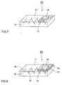
- Fig. 8is a perspective view illustrating a third embodiment of a chip antenna of the present invention.
- a chip antenna 30is different from the chip antenna 10 in that a trimming electrode is coated with a resin layer. More specifically, the chip antenna 30 is formed of a rectangular prism substrate 11, a conductor 12 spirally wound within the substrate 11 in the longitudinal direction of the substrate 11, a power feeding terminal 13, a trimming electrode 14 formed generally in a rectangle, and a resin layer 31 covering the trimming electrode 14.
- the power feeding terminal 13is formed over surfaces of the substrate 11 in order to apply a voltage to the conductor 12 and is connected to one end of the conductor 12.
- the trimming electrode 14is provided within the substrate 11 and is connected to the other end of the conductor 12.
- the trimming electrodeis covered with a resin layer, thereby improving environment-resistance characteristics and further enhancing the reliability of the chip antenna.
- the substrate of the chip antenna or the substrate of the antenna unitis made of a dielectric material essentially consisting of barium oxide, aluminum oxide, and silica.
- the substrateis not restricted to the above type of dielectric material, and may be made of a dielectric material essentially consisting of titanium oxide and neodymium oxide, a magnetic material essentially consisting of nickel, cobalt and iron, or a combination of a dielectric material and a magnetic material.
- the resulting chip antennahas a plurality of resonant frequencies in accordance with the number of conductors, thereby making it possible to cope with multi bands in one chip antenna or in one antenna unit.
- the trimming electrodeis formed generally in the shape of a rectangle, it may be linear, or formed generally in the shape of a circle, an ellipse, or a polygon. Alternatively, the trimming electrode may be formed in an internally hollowed-out shape, a comb-like shape, or a group-like shape, as shown in Figs. 9(a) through 9(c), respectively.
- the conductoris formed within or on the surface of the substrate.
- a spiral or meandering conductormay be formed both on a surface and within the substrate.
- a laseris used to cut the trimming electrode. Additionally, a sandblaster or a toother may be used.
Landscapes
- Details Of Aerials (AREA)
Abstract
Description
The present invention relates to a chip antenna and amethod for adjusting a frequency of the chip antenna. Moreparticularly, the invention relates to a chip antenna usedin mobile communication equipment for mobile communicationsand local area networks (LAN). The invention is alsoconcerned with a method for for adjusting a frequency of theabove type of chip antenna.
Fig. 10 is a side perspective view illustrating aconventional chip antenna. Achip antenna 50 is formed of arectangular-prism insulator 51, aconductor 52, amagneticmember 53, andexternal connecting terminals insulator 51 is formed by laminating insulating layers(not shown) made of an insulating powder, such as alumina orsteatite. Theconductor 52 is made of, for example, silveror silver-palladium, formed in the shape of a coil withintheinsulator 51. Themagnetic member 53 is made of a magnetic powder, such as a ferrite powder, and is formedwithin theinsulator 51 and the coil-like conductor 52. Theexternal connectingterminals conductor 52 and burnedafter theinsulator 51 is fired.
The above known type of chip antenna is miniaturizedcompared with a whip antenna, which is commonly used formobile communications. Accordingly, this chip antenna issurface-mountable. The bandwidth of the chip antenna, onthe other hand, is comparatively narrow. In themanufacturing process, therefore, a deviation of theresonant frequency from a predetermined value seriouslyreduces the gain of the chip antenna, thereby lowering theyield of the chip antenna.
Accordingly, in order to overcome the above problem, itis an object of the present invention to provide a chipantenna in which adjustments are easily made to ensure apredetermined resonant frequency, and also to provide amethod for adjusting a frequency of the chip antenna.
The present invention provides a chip antennacomprising: a substrate made of at least one of dielectricmaterial and a magnetic material; at least one conductordisposed at least one of within said substrate and on a surface of said substrate; at least one power feedingterminal disposed on a surface of said substrate andconnected to one end of said conductor for applying avoltage to said conductor; and a trimming electrode disposedat least one of within said substrate and on a surface ofsaid substrate and connected to the other end of saidconductor.
Since a trimming electrode connected to the other endof a conductor is provided, a capacitive coupling is formedbetween the trimming electrode and each of the conductor anda ground of a mobile communication unit on which the chipantenna is mounted. Accordingly, by adjusting the area ofthe trimming electrode, the amount of the capacitivecoupling can be adjustable, thereby making it possible toadjust the resonant frequency of the chip antenna. As aresult, the resonant frequency is easily adjustable in themanufacturing process of the chip antenna, thereby improvingthe yield of the chip antenna.
The above described chip antenna may further comprise aresin layer covering said trimming electrode.
Since the trimming electrode is coated with a resinlayer, the environment-resistance and characteristics areimproved and further the reliability of the chip antenna isenhanced.
In the above described chip antenna, said substrate may be formed by laminating a plurality of layers together,the layers each having a major surface; and said trimmingelectrode may be disposed on one of the major surfaces ofsaid layers.
In the above described chip antenna, said substrate maybe formed by laminating a plurality of layers together, thelayers each having a major surface and the substrate havinga laminating direction normal to the major surface; and saidconductor may be spiral shaped and having a spiral axisdisposed perpendicular to the laminating direction of saidsubstrate.
In the above described chip antenna, said conductor maybe formed in a plane on one of a surface of the substrate ina meander shape.
The present invention further provides a method foradjusting a frequency of the above described chip antenna,comprising the steps of: changing an area of said trimmingelectrode.
In the above described method, the area of saidtrimming electrode may be changed by using a laser.
By adjusting the area of the trimming electrodeconnected to the other end of the conductor, the capacitivecoupling can be adjustable, thereby making it possible toregulate the resonant frequency of the chip antenna. As aconsequence, the resonant frequency is easily adjustable in the manufacturing process of the chip antenna, therebyenhancing the yield of the chip antenna.
Fig. 1 is a perspective view illustrating a firstembodiment of a chip antenna of the present invention.
Fig. 2 is an exploded perspective view illustrating thechip antenna shown in Fig. 1.
Fig. 3 is a perspective view illustrating an example ofmodifications made to the chip antenna shown in Fig. 1.
Fig. 4 is a perspective view illustrating anotherexample of modifications made to the chip antenna shown inFig. 1.
Fig. 5 is a diagram illustrating the relationshipbetween the area of the trimming electrode and the resonantfrequency of the chip antenna.
Fig. 6 is a perspective view illustrating a secondembodiment of a chip antenna of the present invention.
Fig. 7 is a perspective view illustrating the chipantenna shown in Fig. 1 provided with the partially cuttrimming electrode.
Fig. 8 is a perspective view illustrating a thirdembodiment of a chip antenna of the present invention.
Figs. 9(a) is a top view illustrating an internallyhollowed-out shape as an example of a modification made to the trimming electrode.
Figs. 9(b) is a top view illustrating a comb-like shapeas an example of a modification made to the trimmingelectrode.
Figs. 9(c) is a top view illustrating a group-likeshape as an example of a modification made to the trimmingelectrode.
Fig. 10 is a perspective side view illustrating a knownchip antenna.
Other features and advantages of the present inventionwill become apparent from the following description ofpreferred embodiments of the invention which refers to theaccompanying drawings, wherein like reference numeralsindicate like elements to avoid duplicative description.
Figs. 1 and 2 are respectively a perspective view andan exploded perspective view illustrating a first embodimentof a chip antenna of the present invention. Achip antenna 10 is formed of a rectangular-prism substrate 11 having amounting surface 111, aconductor 12, apower feedingterminal 13, and atrimming electrode 14 formed generally inthe shape of a rectangle and provided on the surface of thesubstrate 11. Theconductor 12 is spirally wound within thesubstrate 11, the winding axis C being positioned in thedirection parallel to themounting surface 111, i.e., in thelongitudinal direction of thesubstrate 11. Thepowerfeeding terminal 13 is formed over surfaces of thesubstrate 11 in order to apply a voltage to theconductor 12. Theconductor 12 is connected at one end to thepower feedingterminal 13 and at the other end to thetrimming electrode 14. With this configuration, a capacitive coupling isgenerated between thetrimming electrode 14 and a ground(not shown) of a mobile communication unit on which thechipantenna 10 is mounted, and between thetrimming electrode 14and theconductor 12.
Thesubstrate 11 is formed by laminatingrectangularsheet layers 15a through 15c made of a dielectric material(relative magnetic permeability: approximately 6.1)essentially consisting of barium oxide, aluminum oxide, andsilica.Conductor patterns 16a through 16h formed in astraight line or generally an L shape and made of copper ora copper alloy are provided on the surfaces of thesheetlayers sheetlayer 15c by means such as printing, vapor-depositing,laminating, or plating is the trimmingelectrode 14generally formed in a rectangle and made of copper or a copper alloy. Further, via-holes 17 are provided atpredetermined positions (at both ends of each of theconductor patterns 16e through 16g and one end of theconductor pattern 16h) on thesheet layer 15b and at apredetermined position (the vicinity of one end of thetrimming electrode 14) on thesheet layer 15c.
Then, thesheet layers 15a through 15c are laminatedand sintered, and theconductor patterns 16a through 16h areconnected through the via-holes 17, thereby forming theconductor 12 having a rectangular shape in winding crosssection and spirally wound within thesubstrate 11 in thelongitudinal direction of thesubstrate 11. Further, thetrimming electrode 14 generally formed in a rectangle isformed on the surface of thesubstrate 11.
One end of the conductor 12 (one end of theconductorpattern 16a) is led to the surface of thesubstrate 11 so asto form apower supply section 18 and is connected to thepower feeding terminal 13 which is provided over thesurfaces of thesubstrate 11 to apply a voltage to theconductor 12. The other end of the conductor 12 (one end oftheconductor pattern 16h) is connected to thetrimmingelectrode 14 through the via-hole 17 within thesubstrate 11.
Figs. 3 and 4 are respectively perspective viewsillustrating examples of modifications made to the chipantenna shown in Fig. 1. Achip antenna 10a shown in Fig. 3 is formed of a rectangular-prism substrate 11a, aconductor 12a, apower feeding terminal 13a, and atrimming electrode 14a generally formed in the shape of a rectangle. Theconductor 12a is spirally wound along the surfaces of thesubstrate 11 in the longitudinal direction of thesubstrate 11. Thepower feeding terminal 13a is provided over thesurfaces of thesubstrate 11 in order to apply a voltage totheconductor 12a and is connected to one end of theconductor 12a. The trimmingelectrode 14a generally formedin a rectangle is provided within thesubstrate 11 and isconnected to the other end of theconductor 12a. With theabove configuration, a capacitive coupling is formed betweenthe trimmingelectrode 14a and a ground (not shown) of amobile communication unit on which thechip antenna 10a ismounted, and between the trimmingelectrode 14 and theconductor 12a. In this modification, the conductor is easyto spirally form on the surfaces of a substrate by meanssuch as screen printing, thereby simplifying themanufacturing process of the chip antenna.
Achip antenna 10b shown in Fig. 4 is formed of arectangular prism substrate 11b, a meanderingconductor 12bformed on the surface (one main surface) of thesubstrate 11b, apower feeding terminal 13b, and a trimmingelectrode 14b formed generally in a rectangle. Thepower feedingterminal 13b is disposed over the surfaces of thesubstrate 11b in order to apply a voltage to theconductor 12b and isconnected to one end of theconductor 12b. The trimmingelectrode 14b is formed on the surface of thesubstrate 11band is connected to the other end of theconductor 12b.With the above configuration, a capacitor element is formedbetween the trimmingelectrode 14b and a ground (not shown)of a mobile communication unit on which thechip antenna 10bis mounted, and between the trimmingelectrode 14b and theconductor 12b. In this modification, since a meanderingconductor is formed only on one main surface of thesubstrate, the height of the substrate becomes smaller,thereby decreasing the height of the chip antenna. Itshould be noted that a meandering conductor may be providedwithin the substrate.
Fig. 5 is a perspective view illustrating a secondembodiment of a chip antenna of the present invention. Achip antenna 20 differs from thechip antenna 10 in that atrimming electrode is provided within a substrate. Morespecifically, thechip antenna 20 is formed of arectangularprism substrate 11, aconductor 12 spirally wound within thesubstrate 11 in the longitudinal direction of thesubstrate 11, apower feeding terminal 13, and a trimmingelectrode 21generally formed in a rectangle. Thepower feeding terminal 13 is provided over surfaces of thesubstrate 11 in order toapply a voltage to theconductor 12 and is connected to one end of theconductor 12. The trimmingelectrode 21 isprovided within thesubstrate 11 and is connected to theother end of theconductor 12. With the above construction,a capacitive coupling is formed between the trimmingelectrode 21 and a ground (not shown) of a mobilecommunication unit on which thechip antenna 20 is mountedand between the trimmingelectrode 21 and theconductor 12.
According to the manufacturing method for the trimmingelectrode 21, in a chip antenna, such as the one shown inFig. 2, the trimmingelectrode 21 is formed together withtheconductor patterns 16e through 16g on the surface of thesheet layer 15b.
Fig. 6 illustrates the relationship between themeasured area S (mm2) of the trimming electrode and theresonant frequency f (GHz) of the chip antenna. Therelative dielectric constant of a dielectric material forthe substrate is approximately 6.1.
Fig. 6 reveals that an increase in the area of thetrimming electrode decreases the resonant frequency. Morespecifically, a trimming electrode having an area of about16.8 (mm2) is formed on a chip antenna having a resonantfrequency of about 880 (MHz), thereby reducing the resonantfrequency to be approximately 615 (MHz).
A method for adjusting the resonant frequency in themanufacturing process for actual products is explained as an example by referring to thechip antenna 10 of the firstembodiment. A trimmingelectrode 14 having a predeterminedarea is cut by laser, as illustrated in Fig. 7, therebydecreasing the area of the trimmingelectrode 14 andincreasing the resonant frequency of thechip antenna 10.
In a chip antenna, such as the one 20 shown in Fig. 5,the trimmingelectrode 21 formed within thesubstrate 11 iscut together with thesubstrate 11.
The foregoing adjustment for the resonant frequency isexplained below by using an equation. When the inductancecomponent of the conductor is indicated by L, and acapacitive coupling generated between the end of theconductor connected to the trimming electrode and a groundof a mobile communication unit on which the chip antenna ismounted is represented by C1, a capacitive couplinggenerated between the trimming electrode and a ground of themobile communication unit on which the chip antenna ismounted is designated by C2, and a capacitive couplinggenerated between the trimming electrode and the conductoris indicated by C3, the resonant frequency f is expressed bythe following equation.f =12πL (C 1+C 2+C 3)
Consequently, the area of the trimming electrode is decreased to reduce the capacitive couplings C2 and C3,thereby increasing the resonant frequency f.
According to the configuration of each of the chipantennas of the foregoing first and second embodiments, atrimming electrode connected to the other end of theconductor is provided. This makes it possible to form acapacitive coupling between the trimming electrode and aconductor and between the trimming electrode and a ground ofa mobile communication unit on which the chip antenna ismounted. Accordingly, by adjusting the area of the trimmingelectrode, the capacitive coupling of the chip antenna isadjustable, thereby enabling the adjustment of the resonantfrequency of the chip antenna. As a consequence, theresonant frequency is easily adjustable in the manufacturingprocess of the chip antenna, thereby improving the yield ofthe chip antenna.
Fig. 8 is a perspective view illustrating a thirdembodiment of a chip antenna of the present invention. Achip antenna 30 is different from thechip antenna 10 inthat a trimming electrode is coated with a resin layer.More specifically, thechip antenna 30 is formed of arectangular prism substrate 11, aconductor 12 spirallywound within thesubstrate 11 in the longitudinal directionof thesubstrate 11, apower feeding terminal 13, a trimmingelectrode 14 formed generally in a rectangle, and aresin layer 31 covering the trimmingelectrode 14. Thepowerfeeding terminal 13 is formed over surfaces of thesubstrate 11 in order to apply a voltage to theconductor 12 and isconnected to one end of theconductor 12. The trimmingelectrode 14 is provided within thesubstrate 11 and isconnected to the other end of theconductor 12.
According to the configuration of the chip antenna ofthe above-described third embodiment, the trimming electrodeis covered with a resin layer, thereby improvingenvironment-resistance characteristics and further enhancingthe reliability of the chip antenna.
In the foregoing chip antennas, the substrate of thechip antenna or the substrate of the antenna unit is made ofa dielectric material essentially consisting of barium oxide,aluminum oxide, and silica. However, the substrate is notrestricted to the above type of dielectric material, and maybe made of a dielectric material essentially consisting oftitanium oxide and neodymium oxide, a magnetic materialessentially consisting of nickel, cobalt and iron, or acombination of a dielectric material and a magnetic material.
Although only one conductor is provided for theforegoing embodiments, a plurality of conductors located inparallel to each other may be provided. In this case, theresulting chip antenna has a plurality of resonantfrequencies in accordance with the number of conductors, thereby making it possible to cope with multi bands in onechip antenna or in one antenna unit.
Moreover, although in the foregoing embodiments, thetrimming electrode is formed generally in the shape of arectangle, it may be linear, or formed generally in theshape of a circle, an ellipse, or a polygon. Alternatively,the trimming electrode may be formed in an internallyhollowed-out shape, a comb-like shape, or a group-like shape,as shown in Figs. 9(a) through 9(c), respectively.
Further, in the foregoing embodiments, the conductor isformed within or on the surface of the substrate. However,a spiral or meandering conductor may be formed both on asurface and within the substrate.
A laser is used to cut the trimming electrode.Additionally, a sandblaster or a toother may be used.
While the invention has been particularly shown anddescribed with reference to preferred embodiments thereof,it will be understood by those skilled man in the art thatthe forgoing and other changes in form and details may bemade therein without departing from the spirit of theinvention.
Claims (7)
- A chip antenna (10;20;30) comprising:a substrate (11) made of at least one of dielectricmaterial and a magnetic material;at least one conductor (12) disposed at least one ofwithin said substrate (11) and on a surface of said substrate(11);at least one power feeding terminal (13) disposed on asurface of said substrate (11) and connected to one end of saidconductor (12) for applying a voltage to said conductor (12);anda trimming electrode (14;21) disposed at least one ofwithin said substrate (11) and on a surface of said substrate(11) and connected to the other end of said conductor (12).
- The chip antenna (30) according to claim 1, furthercomprising a resin layer (31) covering said trimming electrode(14).
- The chip antenna (10) according to claim 1, wherein:said substrate (11) is formed by laminating a plurality oflayers (15a-c) together, the layers (15a-c) each having a majorsurface; andsaid trimming electrode (14) is disposed on one of themajor surfaces of said layers (15a-c).
- The chip antenna (10) according to claim 1, wherein:said substrate (11) is formed by laminating a plurality oflayers (15a-c) together, the layers (15a-c) each having a majorsurface and the substrate (11) having a laminating directionnormal to the major surface; andsaid conductor (12) are spiral shaped and having a spiralaxis (C) disposed perpendicular to the laminating direction ofsaid substrate (11).
- The chip antenna (10) according to claim 1, wherein:said conductor (12) is formed in a plane on one of a surface ofthe substrate (11) in a meander shape.
- A method for adjusting a frequency of the chipantenna (10;20;30) according to claim 1, comprising the stepsof:changing an area of said trimming electrode (14; 21).
- The method according to claim 6, wherein:the area of said trimming electrode (14;21) is changed by usinga laser.
Applications Claiming Priority (2)
| Application Number | Priority Date | Filing Date | Title |
|---|---|---|---|
| JP9050521AJPH10247808A (en) | 1997-03-05 | 1997-03-05 | Chip antenna and frequency adjustment method therefor |
| JP50521/97 | 1997-03-05 |
Publications (2)
| Publication Number | Publication Date |
|---|---|
| EP0863570A2true EP0863570A2 (en) | 1998-09-09 |
| EP0863570A3 EP0863570A3 (en) | 1999-05-19 |
Family
ID=12861294
Family Applications (1)
| Application Number | Title | Priority Date | Filing Date |
|---|---|---|---|
| EP98103733AWithdrawnEP0863570A3 (en) | 1997-03-05 | 1998-03-03 | A chip antenna and a method for adjusting frequency of the same |
Country Status (3)
| Country | Link |
|---|---|
| US (1) | US6064351A (en) |
| EP (1) | EP0863570A3 (en) |
| JP (1) | JPH10247808A (en) |
Cited By (12)
| Publication number | Priority date | Publication date | Assignee | Title |
|---|---|---|---|---|
| WO2001080355A1 (en)* | 2000-04-18 | 2001-10-25 | Telefonaktiebolaget Lm Ericsson (Publ) | A multi-band antenna for use in a portable telecommunication apparatus |
| EP1178565A1 (en)* | 2000-07-31 | 2002-02-06 | Murata Manufacturing Co., Ltd. | Chip antenna |
| EP1198027A1 (en)* | 2000-10-12 | 2002-04-17 | The Furukawa Electric Co., Ltd. | Small antenna |
| EP1202383A2 (en)* | 2000-10-31 | 2002-05-02 | Mitsubishi Materials Corporation | Antenna, receiving/transmitting apparatus therewith and method of manufacturing the antenna |
| EP1181741A4 (en)* | 1999-05-13 | 2002-07-17 | Cera Inc K | Helical antenna manufacturing apparatus and method thereof |
| EP1270168A3 (en)* | 2001-06-25 | 2003-05-14 | The Furukawa Electric Co., Ltd. | Chip antenna and method of manufacturing the same |
| EP1178561A3 (en)* | 2000-08-04 | 2004-10-27 | Mitsubishi Materials Corporation | Antenna |
| EP1430563A4 (en)* | 2001-01-06 | 2005-02-09 | Telisar Corp | An integrated antenna system |
| WO2005096433A3 (en)* | 2004-04-01 | 2005-12-22 | Kathrein Werke Kg | Embedded planar antenna and pertaining tuning method |
| DE10114012B4 (en)* | 2000-05-11 | 2011-02-24 | Amtran Technology Co., Ltd., Chung Ho | chip antenna |
| EP1202382B1 (en)* | 2000-10-31 | 2011-12-07 | Mitsubishi Materials Corporation | Antenna |
| WO2018180839A1 (en)* | 2017-03-29 | 2018-10-04 | 株式会社ヨコオ | Antenna device |
Families Citing this family (38)
| Publication number | Priority date | Publication date | Assignee | Title |
|---|---|---|---|---|
| US6621194B1 (en)* | 1999-11-15 | 2003-09-16 | Matsushita Electric Industrial Co., Ltd. | Piezoelectric element having thickness shear vibration and mobile communication device using the same |
| KR100702088B1 (en)* | 2000-01-31 | 2007-04-02 | 미츠비시 마테리알 가부시키가이샤 | Antenna device and antenna device assembly |
| US6653978B2 (en)* | 2000-04-20 | 2003-11-25 | Nokia Mobile Phones, Ltd. | Miniaturized radio frequency antenna |
| US6486853B2 (en)* | 2000-05-18 | 2002-11-26 | Matsushita Electric Industrial Co., Ltd. | Chip antenna, radio communications terminal and radio communications system using the same and method for production of the same |
| JP2002043881A (en)* | 2000-07-31 | 2002-02-08 | Murata Mfg Co Ltd | Laminated lc filter and frequency control method therefor |
| JP2002141734A (en)* | 2000-10-31 | 2002-05-17 | Mitsubishi Materials Corp | antenna |
| DE60120894T2 (en)* | 2000-12-26 | 2007-01-11 | The Furukawa Electric Co., Ltd. | Manufacturing method of an antenna |
| US6421015B1 (en)* | 2001-01-02 | 2002-07-16 | Auden Techno Corp | Planar helix antenna with two frequencies |
| JP2002232223A (en)* | 2001-02-01 | 2002-08-16 | Nec Corp | Chip antenna and antenna device |
| KR100423395B1 (en)* | 2001-07-02 | 2004-03-18 | 삼성전기주식회사 | A Chip Antenna |
| TW516718U (en)* | 2001-08-10 | 2003-01-01 | Hon Hai Prec Ind Co Ltd | Printed antenna |
| US6995710B2 (en)* | 2001-10-09 | 2006-02-07 | Ngk Spark Plug Co., Ltd. | Dielectric antenna for high frequency wireless communication apparatus |
| US6842158B2 (en)* | 2001-12-27 | 2005-01-11 | Skycross, Inc. | Wideband low profile spiral-shaped transmission line antenna |
| US7042418B2 (en)* | 2002-11-27 | 2006-05-09 | Matsushita Electric Industrial Co., Ltd. | Chip antenna |
| TWI247451B (en)* | 2002-11-29 | 2006-01-11 | Tdk Corp | Chip antenna, chip antenna unit and wireless communication device using the same |
| EP2273611B1 (en) | 2002-12-22 | 2012-02-08 | Fractus, S.A. | Multi-band monopole antenna for a mobile communications device |
| WO2004075343A1 (en) | 2003-02-18 | 2004-09-02 | Tadahiro Ohmi | Antenna for portable terminal and portable terminal using same |
| WO2004091039A2 (en)* | 2003-04-10 | 2004-10-21 | Matsushita Electric Industrial Co. Ltd. | Antenna element and antenna module, and electronic equipment using same |
| TWI220077B (en)* | 2003-07-15 | 2004-08-01 | High Tech Comp Corp | Multi-frequency antenna |
| KR20060119914A (en)* | 2003-09-01 | 2006-11-24 | 마츠시타 덴끼 산교 가부시키가이샤 | Antenna module |
| TWI235524B (en)* | 2003-11-24 | 2005-07-01 | Jeng-Fang Liou | Planar antenna |
| JP2005175757A (en)* | 2003-12-10 | 2005-06-30 | Matsushita Electric Ind Co Ltd | Antenna module |
| EP1709704A2 (en) | 2004-01-30 | 2006-10-11 | Fractus, S.A. | Multi-band monopole antennas for mobile communications devices |
| US7307597B2 (en)* | 2004-03-17 | 2007-12-11 | Matsushita Electric Industrial Co., Ltd. | Antenna |
| US7113135B2 (en)* | 2004-06-08 | 2006-09-26 | Skycross, Inc. | Tri-band antenna for digital multimedia broadcast (DMB) applications |
| US7102587B2 (en)* | 2004-06-15 | 2006-09-05 | Premark Rwp Holdings, Inc. | Embedded antenna connection method and system |
| US7079079B2 (en)* | 2004-06-30 | 2006-07-18 | Skycross, Inc. | Low profile compact multi-band meanderline loaded antenna |
| CN100397704C (en)* | 2004-11-25 | 2008-06-25 | 刘正芳 | Multiband Planar Antenna |
| US7057565B1 (en)* | 2005-04-18 | 2006-06-06 | Cheng-Fang Liu | Multi-band flat antenna |
| US20060284770A1 (en)* | 2005-06-15 | 2006-12-21 | Young-Min Jo | Compact dual band antenna having common elements and common feed |
| KR100638872B1 (en)* | 2005-06-30 | 2006-10-27 | 삼성전기주식회사 | Integrated chip antenna |
| EP2124291B1 (en)* | 2005-10-19 | 2013-09-18 | D-Per Technologies Ltd. | Antenna arrangement |
| WO2008146932A1 (en)* | 2007-05-29 | 2008-12-04 | Nof Corporation | Antenna |
| US8126410B2 (en)* | 2007-06-07 | 2012-02-28 | Vishay Intertechnology, Inc. | Miniature sub-resonant multi-band VHF-UHF antenna |
| KR100977086B1 (en) | 2008-03-31 | 2010-08-19 | 전남대학교산학협력단 | Broadband mini antenna |
| JP4853569B2 (en)* | 2009-11-13 | 2012-01-11 | パナソニック株式会社 | Antenna module |
| US10074888B2 (en)* | 2015-04-03 | 2018-09-11 | NXT-ID, Inc. | Accordion antenna structure |
| US20250233302A1 (en)* | 2024-01-12 | 2025-07-17 | Tdk Corporation | Antenna device and ic card provided therewith |
Citations (2)
| Publication number | Priority date | Publication date | Assignee | Title |
|---|---|---|---|---|
| US4701763A (en)* | 1984-09-17 | 1987-10-20 | Matsushita Electric Industrial Co., Ltd. | Small antenna |
| JPH04129302A (en)* | 1990-09-19 | 1992-04-30 | Matsushita Electric Ind Co Ltd | Antenna for radio equipment |
Family Cites Families (9)
| Publication number | Priority date | Publication date | Assignee | Title |
|---|---|---|---|---|
| CH499888A (en)* | 1967-12-15 | 1970-11-30 | Onera (Off Nat Aerospatiale) | Helically wound single conductor antenna of reduced dimensions, and method for its manufacture |
| JPS61111563A (en)* | 1984-11-05 | 1986-05-29 | Mitsubishi Electric Corp | Method of metallic wiring cut of semiconductor device |
| JP3308558B2 (en)* | 1991-05-02 | 2002-07-29 | 富士通株式会社 | Antenna module |
| US5561437A (en)* | 1994-09-15 | 1996-10-01 | Motorola, Inc. | Two position fold-over dipole antenna |
| JP3123363B2 (en)* | 1994-10-04 | 2001-01-09 | 三菱電機株式会社 | Portable radio |
| AU3677795A (en)* | 1995-04-26 | 1996-11-18 | Westinghouse Electric Corporation | Helical antenna having a parasitic element and a method of u sing the same |
| CN1150660C (en)* | 1995-06-02 | 2004-05-19 | 艾利森公司 | Multiple band printed monopole antenna |
| JPH0951221A (en)* | 1995-08-07 | 1997-02-18 | Murata Mfg Co Ltd | Chip antenna |
| JPH1098322A (en)* | 1996-09-20 | 1998-04-14 | Murata Mfg Co Ltd | Chip antenna and antenna system |
- 1997
- 1997-03-05JPJP9050521Apatent/JPH10247808A/enactivePending
- 1998
- 1998-03-03EPEP98103733Apatent/EP0863570A3/ennot_activeWithdrawn
- 1998-03-04USUS09/034,416patent/US6064351A/ennot_activeExpired - Lifetime
Patent Citations (2)
| Publication number | Priority date | Publication date | Assignee | Title |
|---|---|---|---|---|
| US4701763A (en)* | 1984-09-17 | 1987-10-20 | Matsushita Electric Industrial Co., Ltd. | Small antenna |
| JPH04129302A (en)* | 1990-09-19 | 1992-04-30 | Matsushita Electric Ind Co Ltd | Antenna for radio equipment |
Cited By (24)
| Publication number | Priority date | Publication date | Assignee | Title |
|---|---|---|---|---|
| EP1181741A4 (en)* | 1999-05-13 | 2002-07-17 | Cera Inc K | Helical antenna manufacturing apparatus and method thereof |
| US6788271B1 (en) | 1999-05-13 | 2004-09-07 | K-Cera, Inc. | Helical antenna manufacturing apparatus and method thereof |
| US6504511B2 (en) | 2000-04-18 | 2003-01-07 | Telefonaktiebolaget Lm Ericsson (Publ) | Multi-band antenna for use in a portable telecommunications apparatus |
| WO2001080355A1 (en)* | 2000-04-18 | 2001-10-25 | Telefonaktiebolaget Lm Ericsson (Publ) | A multi-band antenna for use in a portable telecommunication apparatus |
| DE10114012B4 (en)* | 2000-05-11 | 2011-02-24 | Amtran Technology Co., Ltd., Chung Ho | chip antenna |
| EP1178565A1 (en)* | 2000-07-31 | 2002-02-06 | Murata Manufacturing Co., Ltd. | Chip antenna |
| US6583769B2 (en) | 2000-07-31 | 2003-06-24 | Murata Manufacturing Co., Ltd. | Chip antenna |
| EP1178561A3 (en)* | 2000-08-04 | 2004-10-27 | Mitsubishi Materials Corporation | Antenna |
| KR100860281B1 (en)* | 2000-08-04 | 2008-09-25 | 미츠비시 마테리알 가부시키가이샤 | Antenna |
| EP1198027A1 (en)* | 2000-10-12 | 2002-04-17 | The Furukawa Electric Co., Ltd. | Small antenna |
| US6693604B2 (en) | 2000-10-12 | 2004-02-17 | The Furukawa Electric Co., Ltd. | Small antenna |
| EP1202383A2 (en)* | 2000-10-31 | 2002-05-02 | Mitsubishi Materials Corporation | Antenna, receiving/transmitting apparatus therewith and method of manufacturing the antenna |
| EP1202382B1 (en)* | 2000-10-31 | 2011-12-07 | Mitsubishi Materials Corporation | Antenna |
| EP1430563A4 (en)* | 2001-01-06 | 2005-02-09 | Telisar Corp | An integrated antenna system |
| CN100435412C (en)* | 2001-06-25 | 2008-11-19 | 古河电气工业株式会社 | Chip aerial and its manufacturing method |
| US6724347B2 (en) | 2001-06-25 | 2004-04-20 | The Furukawa Electric Co., Ltd. | Chip antenna and method of manufacturing the same |
| EP1270168A3 (en)* | 2001-06-25 | 2003-05-14 | The Furukawa Electric Co., Ltd. | Chip antenna and method of manufacturing the same |
| WO2005096433A3 (en)* | 2004-04-01 | 2005-12-22 | Kathrein Werke Kg | Embedded planar antenna and pertaining tuning method |
| US7626547B2 (en) | 2004-04-01 | 2009-12-01 | Kathrein-Werke Kg | Embedded planar antenna with pertaining tuning method |
| WO2018180839A1 (en)* | 2017-03-29 | 2018-10-04 | 株式会社ヨコオ | Antenna device |
| CN110495052A (en)* | 2017-03-29 | 2019-11-22 | 株式会社友华 | Antenna assembly |
| US11502409B2 (en) | 2017-03-29 | 2022-11-15 | Yokowo Co., Ltd. | Antenna device |
| CN110495052B (en)* | 2017-03-29 | 2023-02-17 | 株式会社友华 | Antenna device |
| US12191577B2 (en) | 2017-03-29 | 2025-01-07 | Yokowo Co., Ltd. | Antenna device |
Also Published As
| Publication number | Publication date |
|---|---|
| US6064351A (en) | 2000-05-16 |
| JPH10247808A (en) | 1998-09-14 |
| EP0863570A3 (en) | 1999-05-19 |
Similar Documents
| Publication | Publication Date | Title |
|---|---|---|
| US6064351A (en) | Chip antenna and a method for adjusting frequency of the same | |
| KR100414765B1 (en) | Ceramic chip antenna | |
| EP0923153B1 (en) | Chip-antenna | |
| EP1267441B1 (en) | Surface-mounted antenna and communications apparatus comprising the same | |
| US6271803B1 (en) | Chip antenna and radio equipment including the same | |
| JP3147756B2 (en) | Chip antenna | |
| WO2009081803A1 (en) | Antenna device and wireless communication device using the same | |
| US20030227411A1 (en) | Chip antenna with parasitic elements | |
| EP0863571A2 (en) | A mobile image apparatus and an antenna apparatus used for the mobile image apparatus | |
| US6653986B2 (en) | Meander antenna and method for tuning resonance frequency of the same | |
| JP4263972B2 (en) | Surface mount antenna, antenna device, and wireless communication device | |
| EP0828310B1 (en) | Antenna device | |
| JP2004023624A (en) | Surface mount antenna and antenna device | |
| EP0802577B1 (en) | Chip antenna | |
| US5764197A (en) | Chip antenna | |
| CN100418268C (en) | Surface mount antennas, antenna equipment and radio communication equipment | |
| JP3644193B2 (en) | Antenna device | |
| JPH09307331A (en) | Matching circuit and antenna system using it | |
| JPH09199939A (en) | Antenna system | |
| JPH0969717A (en) | Chip antenna | |
| JPH0969715A (en) | Chip antenna | |
| JPH10145124A (en) | Chip antenna | |
| JP3528017B2 (en) | Adjustment method of resonance frequency of chip antenna | |
| JPH10154906A (en) | Chip antenna | |
| JP2007129360A (en) | Dielectric antenna |
Legal Events
| Date | Code | Title | Description |
|---|---|---|---|
| PUAI | Public reference made under article 153(3) epc to a published international application that has entered the european phase | Free format text:ORIGINAL CODE: 0009012 | |
| 17P | Request for examination filed | Effective date:19980303 | |
| AK | Designated contracting states | Kind code of ref document:A2 Designated state(s):DE FR GB | |
| AX | Request for extension of the european patent | Free format text:AL;LT;LV;MK;RO;SI | |
| PUAL | Search report despatched | Free format text:ORIGINAL CODE: 0009013 | |
| AK | Designated contracting states | Kind code of ref document:A3 Designated state(s):AT BE CH DE DK ES FI FR GB GR IE IT LI LU MC NL PT SE | |
| AX | Request for extension of the european patent | Free format text:AL;LT;LV;MK;RO;SI | |
| AKX | Designation fees paid | Free format text:DE FR GB | |
| 17Q | First examination report despatched | Effective date:20040917 | |
| GRAP | Despatch of communication of intention to grant a patent | Free format text:ORIGINAL CODE: EPIDOSNIGR1 | |
| STAA | Information on the status of an ep patent application or granted ep patent | Free format text:STATUS: THE APPLICATION HAS BEEN WITHDRAWN | |
| 18W | Application withdrawn | Effective date:20060220 |