EP0860915B1 - Vertical cavity surface emitting laser for high power operation and method of fabrication - Google Patents
Vertical cavity surface emitting laser for high power operation and method of fabricationDownload PDFInfo
- Publication number
- EP0860915B1 EP0860915B1EP98102181AEP98102181AEP0860915B1EP 0860915 B1EP0860915 B1EP 0860915B1EP 98102181 AEP98102181 AEP 98102181AEP 98102181 AEP98102181 AEP 98102181AEP 0860915 B1EP0860915 B1EP 0860915B1
- Authority
- EP
- European Patent Office
- Prior art keywords
- gold
- heat dissipation
- disposed
- vertical cavity
- emitting laser
- Prior art date
- Legal status (The legal status is an assumption and is not a legal conclusion. Google has not performed a legal analysis and makes no representation as to the accuracy of the status listed.)
- Expired - Lifetime
Links
- 238000004519manufacturing processMethods0.000titleclaimsdescription7
- 239000000463materialSubstances0.000claimsdescription48
- 239000010931goldSubstances0.000claimsdescription30
- 230000017525heat dissipationEffects0.000claimsdescription28
- 239000000758substrateSubstances0.000claimsdescription26
- PCHJSUWPFVWCPO-UHFFFAOYSA-NgoldChemical compound[Au]PCHJSUWPFVWCPO-UHFFFAOYSA-N0.000claimsdescription15
- 229910052737goldInorganic materials0.000claimsdescription15
- JBRZTFJDHDCESZ-UHFFFAOYSA-NAsGaChemical compound[As]#[Ga]JBRZTFJDHDCESZ-UHFFFAOYSA-N0.000claimsdescription14
- PXHVJJICTQNCMI-UHFFFAOYSA-NNickelChemical compound[Ni]PXHVJJICTQNCMI-UHFFFAOYSA-N0.000claimsdescription12
- 238000000034methodMethods0.000claimsdescription12
- 229910001218Gallium arsenideInorganic materials0.000claimsdescription11
- 229910001258titanium goldInorganic materials0.000claimsdescription8
- XUIMIQQOPSSXEZ-UHFFFAOYSA-NSiliconChemical compound[Si]XUIMIQQOPSSXEZ-UHFFFAOYSA-N0.000claimsdescription7
- 229910052710siliconInorganic materials0.000claimsdescription7
- 239000010703siliconSubstances0.000claimsdescription7
- 239000011651chromiumSubstances0.000claimsdescription6
- BYDQGSVXQDOSJJ-UHFFFAOYSA-N[Ge].[Au]Chemical compound[Ge].[Au]BYDQGSVXQDOSJJ-UHFFFAOYSA-N0.000claimsdescription5
- HBMJWWWQQXIZIP-UHFFFAOYSA-Nsilicon carbideChemical compound[Si+]#[C-]HBMJWWWQQXIZIP-UHFFFAOYSA-N0.000claimsdescription5
- VYZAMTAEIAYCRO-UHFFFAOYSA-NChromiumChemical compound[Cr]VYZAMTAEIAYCRO-UHFFFAOYSA-N0.000claimsdescription4
- 229910052804chromiumInorganic materials0.000claimsdescription4
- ZNKMCMOJCDFGFT-UHFFFAOYSA-Ngold titaniumChemical compound[Ti].[Au]ZNKMCMOJCDFGFT-UHFFFAOYSA-N0.000claimsdescription4
- SAOPTAQUONRHEV-UHFFFAOYSA-Ngold zincChemical compound[Zn].[Au]SAOPTAQUONRHEV-UHFFFAOYSA-N0.000claimsdescription4
- 229910052759nickelInorganic materials0.000claimsdescription4
- MAKDTFFYCIMFQP-UHFFFAOYSA-Ntitanium tungstenChemical compound[Ti].[W]MAKDTFFYCIMFQP-UHFFFAOYSA-N0.000claimsdescription4
- 230000008569processEffects0.000claimsdescription2
- 239000003989dielectric materialSubstances0.000claims1
- 239000010410layerSubstances0.000description65
- 238000005253claddingMethods0.000description19
- FTWRSWRBSVXQPI-UHFFFAOYSA-Nalumanylidynearsane;gallanylidynearsaneChemical compound[As]#[Al].[As]#[Ga]FTWRSWRBSVXQPI-UHFFFAOYSA-N0.000description17
- 230000004888barrier functionEffects0.000description9
- 229910005540GaPInorganic materials0.000description5
- AUCDRFABNLOFRE-UHFFFAOYSA-Nalumane;indiumChemical compound[AlH3].[In]AUCDRFABNLOFRE-UHFFFAOYSA-N0.000description5
- 238000000151depositionMethods0.000description5
- RNQKDQAVIXDKAG-UHFFFAOYSA-Naluminum galliumChemical compound[Al].[Ga]RNQKDQAVIXDKAG-UHFFFAOYSA-N0.000description4
- 238000012986modificationMethods0.000description4
- 230000004048modificationEffects0.000description4
- MDPILPRLPQYEEN-UHFFFAOYSA-Naluminium arsenideChemical compound[As]#[Al]MDPILPRLPQYEEN-UHFFFAOYSA-N0.000description3
- 230000008021depositionEffects0.000description3
- HZXMRANICFIONG-UHFFFAOYSA-Ngallium phosphideChemical compound[Ga]#PHZXMRANICFIONG-UHFFFAOYSA-N0.000description3
- 229910052751metalInorganic materials0.000description3
- 239000002184metalSubstances0.000description3
- 239000004065semiconductorSubstances0.000description3
- 239000002356single layerSubstances0.000description3
- 229910002601GaNInorganic materials0.000description2
- 229910052782aluminiumInorganic materials0.000description2
- XAGFODPZIPBFFR-UHFFFAOYSA-NaluminiumChemical compound[Al]XAGFODPZIPBFFR-UHFFFAOYSA-N0.000description2
- 230000008859changeEffects0.000description2
- 230000001419dependent effectEffects0.000description2
- 239000002019doping agentSubstances0.000description2
- 238000001451molecular beam epitaxyMethods0.000description2
- 238000000059patterningMethods0.000description2
- 229910010271silicon carbideInorganic materials0.000description2
- OKTJSMMVPCPJKN-UHFFFAOYSA-NCarbonChemical compound[C]OKTJSMMVPCPJKN-UHFFFAOYSA-N0.000description1
- GPXJNWSHGFTCBW-UHFFFAOYSA-NIndium phosphideChemical compound[In]#PGPXJNWSHGFTCBW-UHFFFAOYSA-N0.000description1
- BUGBHKTXTAQXES-UHFFFAOYSA-NSeleniumChemical compound[Se]BUGBHKTXTAQXES-UHFFFAOYSA-N0.000description1
- HCHKCACWOHOZIP-UHFFFAOYSA-NZincChemical compound[Zn]HCHKCACWOHOZIP-UHFFFAOYSA-N0.000description1
- 229910045601alloyInorganic materials0.000description1
- 239000000956alloySubstances0.000description1
- 230000003466anti-cipated effectEffects0.000description1
- 229910052785arsenicInorganic materials0.000description1
- 229910052799carbonInorganic materials0.000description1
- 238000003486chemical etchingMethods0.000description1
- 238000005229chemical vapour depositionMethods0.000description1
- PMHQVHHXPFUNSP-UHFFFAOYSA-Mcopper(1+);methylsulfanylmethane;bromideChemical compoundBr[Cu].CSCPMHQVHHXPFUNSP-UHFFFAOYSA-M0.000description1
- 239000013078crystalSubstances0.000description1
- 230000007812deficiencyEffects0.000description1
- 230000006872improvementEffects0.000description1
- 230000010354integrationEffects0.000description1
- 239000000203mixtureSubstances0.000description1
- 238000002310reflectometryMethods0.000description1
- 239000011669seleniumSubstances0.000description1
- 229910052711seleniumInorganic materials0.000description1
- 238000004544sputter depositionMethods0.000description1
- 239000002470thermal conductorSubstances0.000description1
- 229910052725zincInorganic materials0.000description1
- 239000011701zincSubstances0.000description1
Images

Classifications
- H—ELECTRICITY
- H01—ELECTRIC ELEMENTS
- H01S—DEVICES USING THE PROCESS OF LIGHT AMPLIFICATION BY STIMULATED EMISSION OF RADIATION [LASER] TO AMPLIFY OR GENERATE LIGHT; DEVICES USING STIMULATED EMISSION OF ELECTROMAGNETIC RADIATION IN WAVE RANGES OTHER THAN OPTICAL
- H01S5/00—Semiconductor lasers
- H01S5/10—Construction or shape of the optical resonator, e.g. extended or external cavity, coupled cavities, bent-guide, varying width, thickness or composition of the active region
- H01S5/18—Surface-emitting [SE] lasers, e.g. having both horizontal and vertical cavities
- H01S5/183—Surface-emitting [SE] lasers, e.g. having both horizontal and vertical cavities having only vertical cavities, e.g. vertical cavity surface-emitting lasers [VCSEL]
- H—ELECTRICITY
- H01—ELECTRIC ELEMENTS
- H01S—DEVICES USING THE PROCESS OF LIGHT AMPLIFICATION BY STIMULATED EMISSION OF RADIATION [LASER] TO AMPLIFY OR GENERATE LIGHT; DEVICES USING STIMULATED EMISSION OF ELECTROMAGNETIC RADIATION IN WAVE RANGES OTHER THAN OPTICAL
- H01S5/00—Semiconductor lasers
- H01S5/02—Structural details or components not essential to laser action
- H01S5/0206—Substrates, e.g. growth, shape, material, removal or bonding
- H01S5/021—Silicon based substrates
- H—ELECTRICITY
- H01—ELECTRIC ELEMENTS
- H01S—DEVICES USING THE PROCESS OF LIGHT AMPLIFICATION BY STIMULATED EMISSION OF RADIATION [LASER] TO AMPLIFY OR GENERATE LIGHT; DEVICES USING STIMULATED EMISSION OF ELECTROMAGNETIC RADIATION IN WAVE RANGES OTHER THAN OPTICAL
- H01S5/00—Semiconductor lasers
- H01S5/02—Structural details or components not essential to laser action
- H01S5/0206—Substrates, e.g. growth, shape, material, removal or bonding
- H01S5/0215—Bonding to the substrate
- H—ELECTRICITY
- H01—ELECTRIC ELEMENTS
- H01S—DEVICES USING THE PROCESS OF LIGHT AMPLIFICATION BY STIMULATED EMISSION OF RADIATION [LASER] TO AMPLIFY OR GENERATE LIGHT; DEVICES USING STIMULATED EMISSION OF ELECTROMAGNETIC RADIATION IN WAVE RANGES OTHER THAN OPTICAL
- H01S5/00—Semiconductor lasers
- H01S5/02—Structural details or components not essential to laser action
- H01S5/0206—Substrates, e.g. growth, shape, material, removal or bonding
- H01S5/0217—Removal of the substrate
- H—ELECTRICITY
- H01—ELECTRIC ELEMENTS
- H01S—DEVICES USING THE PROCESS OF LIGHT AMPLIFICATION BY STIMULATED EMISSION OF RADIATION [LASER] TO AMPLIFY OR GENERATE LIGHT; DEVICES USING STIMULATED EMISSION OF ELECTROMAGNETIC RADIATION IN WAVE RANGES OTHER THAN OPTICAL
- H01S5/00—Semiconductor lasers
- H01S5/02—Structural details or components not essential to laser action
- H01S5/024—Arrangements for thermal management
- H01S5/02476—Heat spreaders, i.e. improving heat flow between laser chip and heat dissipating elements
Definitions
- This inventionrelates to vertical cavity surface emitting lasers and more specifically to vertical cavity surface emitting lasers for high power operation.
- VCSELVertical cavity surface emitting lasers
- DBRdistributed Bragg reflector
- the VCSELis driven by current forced through the active region, typically achieved by providing a first contact on the reverse side of the substrate and a second contact on top of the second mirror stack.
- mirror stacksare formed of multiple pairs of layers often referred to as mirror pairs.
- the pairs of layersare formed of a material system generally consisting of two materials having different indices of refraction and being easily lattice matched to the other portions of the VCSEL.
- a GaAs based VCSELtypically uses an Al x1 Ga 1-x1 As ⁇ Al x2 Ga 1-x2 As material system wherein the different refractive index of each layer of a pair is achieved by altering the aluminum content x1 and x2 in the layers.
- the number of mirror pairs per stackmay range from 20-40 pairs to achieve a high percentage of reflectivity, depending on the difference between the refractive indices of the layers. The large number of pairs increases the percentage of reflected light.
- VCSELsIn conventional VCSELs, conventional material systems perform adequately. Such a VCSEL is disclosed in US-5146465, where the aluminum gallium nitride laser has an active region that is composed of aluminum gallium nitride material, and a buffer layer that is composed of aluminum nitride.
- new productsare being developed, such as CD write devices and those utilizing infra-red data links, that require VCSELs to operate at a higher power, i.e. greater than 20 milliwatts.
- the GaAs substrateis absorptive with a laser emission being toward the opposite direction, the top.
- the GaAs substrateis not a good thermal conductor and thereby causes the heat to accumulate near the active region. This in turn causes a temperature rise which saturates the laser output power. Therefore, it becomes difficult to generate high power from this type of VCSEL, especially at ambient temperatures, i.e. 50-60 °C.
- VCSELvertical cavity surface emitting laser
- Another object of the inventionis to provide a reliable high power VCSEL.
- Another object of the immediate inventionis to provide for an efficient heat dissipator for use in a high power VCSEL.
- Still another object of the inventionis to provide for a smaller degree of thermal resistance in a high power VCSEL.
- Yet another object of the inventionis to provide for a highly manufacturable high power VCSEL.
- a VCSELfor use in high power operation.
- the VCSELas defined in Claims 1-9, generally includes a silicon substrate made from Si or SiC, a heat dissipation layer, a first stack of distributed Bragg reflectors, an active region, and a second stack of distributed Bragg reflectors.
- the heat dissipation layeris composed of a gold germanium (AuGe) or a gold (Au) material to efficiently dissipate heat from the active region into the silicon substrate made from Si or SiC.
- AuGegold germanium
- Augold
- FIG. 1illustrates the fabrication of a first vertical cavity surface emitting laser (VCSEL) wafer structure generally designated 10.
- Wafer structure 10is formed on a substrate 12, which in this specific embodiment is gallium arsenide (GaAs).
- GaAsis preferably used to facilitate lattice matching of the components of wafer structure 10 which emits infrared wavelength light, more particularly 780nm or 850nm light, dependent upon the specific material system used.
- GaAsis utilized so as to facilitate epitaxial growth of subsequent multiple layers that compose wafer structure 10. It should be understood that GaAs is only utilized as an example and other semiconductor materials may be employed as substrate 12, such as silicon (Si), indium phosphide (InP), or the like.
- any suitable epitaxial deposition methodsuch as molecular beam epitaxy (MBE), metal organic chemical vapor deposition (MOCVD), or the like is used to make the required multiple layers for wafer structure 10.
- MBEmolecular beam epitaxy
- MOCVDmetal organic chemical vapor deposition
- material layerssuch as aluminum gallium arsenide, aluminum arsenide, indium aluminum gallium phosphide, gallium arsenide, and aluminum arsenide, or aluminum gallium phosphide, indium aluminum phosphide, and the like. It should be understood that epitaxial deposition is used extensively to produce the multitude of layers that comprise the complete VCSEL device of the present invention.
- Substrate 12has an upper surface 13 on which a buffer layer 14 is disposed.
- Buffer layer 14includes a p-doped gallium arsenide (GaAs) material.
- an etch stop layer 16is disposed on buffer layer 14.
- Etch stop layer 16includes an aluminum gallium arsenide (AlGaAs) material or an aluminum gallium phosphide (AlGaP) material. Buffer layer 14 and etch stop layer 16 will aid in the removal of substrate 12 during the fabrication of the complete VCSEL for high power operation of the present invention.
- a first mirror stack 18is disposed on etch stop layer 16.
- An active region 21is disposed on mirror stack 18.
- Active region 21includes an active structure 22 sandwiched between a first cladding region 23 adjacent first mirror stack 18 and a second cladding region 24.
- a second mirror stack 26is disposed on second cladding region 24.
- distributed Bragg reflector 18is deposited first with subsequent deposition defining cladding region 23, active structure 22, cladding region 24, distributed Bragg reflector 26 and a heat dissipation layer 30.
- thicknesses of alternating layers 19, 20, 27, and 28are typically set as portions of a wavelength of light (not shown) that the complete VCSEL device is designed to emit.
- specific thicknesses of the alternating layers 19, 20, 27 and 28are a function of the designed wavelength at which the VCSEL is to operate.
- the most common wavelength values usedare one-quarter, one-half, three-quarters, full wavelength, or any multiples thereof. In a preferred embodiment of the present invention, one-quarter wavelength thicknesses are used.
- doping of the distributed Bragg reflectors 18 and 26is split with one of the distributed Bragg reflectors being N-type and the other being P-type. Since doping levels are well known in the art, the doping levels will not be described herein other than to identify material either as undoped, P-typed doped such as with carbon, zinc or the like, or N-typed doped such as with selenium, silicon, or the like.
- distributed Bragg reflector 18 and a portion of cladding region 23are P-typed doped, with a portion of cladding region 23, active structure 22, and a portion of cladding region 24 being undoped, and with a portion of cladding region 24, and distributed Bragg reflector 26 being N-typed doped.
- distributed Bragg reflectors 18 and 26 having alternating layers 19 and 20, 27 and 28are made of any suitable materials, such as aluminum gallium arsenide (AlGaAs) with the aluminum percentage ranging from 0 to 100% or materials forming a dielectric mirror stack. More specifically, a VCSEL structure designed to emit at 780nm will include alternating layers 19, 20, 27, and 28 of Al .25 Ga .75 As/Al .95 Ga .05 As or Al .25 Ga .75 As/AlAs. A VCSEL structure designed to emit at 850 nm will include alternating layers 19, 20, 27 and 28 of Al .15 Ga .85 As/Al .85 Ga .15 As.
- AlGaAsaluminum gallium arsenide
- layers 19 and 20are epitaxially disposed or deposited on or overlaying etch stop layer 16 and layers 27 and 28 are epitaxially disposed or deposited on or overlaying cladding region 24, thereby generating distributed Bragg reflectors 18 and 26.
- Mirror stack 18 and 26are formed by depositing pairs of alternating layers using some convenient technique such as molecular beam epitaxy (MBE) or sputtering. In order to crystal lattice match mirror stack 18 to substrate 12 a suitable semiconductor material system must be deposited. Approximately 20-40 mirror pairs of this material system are deposited on etch stop layer 16 depending on the difference between the refractive indices of the layers. As will be explained presently, doping the mirror stacks is not necessary since electrical contacts to the active region can be made laterally.
- MBEmolecular beam epitaxy
- sputteringIn order to crystal lattice match mirror stack 18 to substrate 12 a suitable semiconductor material system must be deposited. Approximately 20-40 mirror pairs of this material system are deposited on etch stop layer 16 depending on the difference between the refractive indices of the layers. As will be explained presently, doping the mirror stacks is not necessary since electrical contacts to the active region can be made laterally.
- cladding region 23is shown as a single layer; however, it should be understood that cladding region 23 is made of at least two components that are epitaxially disposed or deposited on distributed Bragg reflector 18.
- a layer of any suitable materialsuch as aluminum gallium arsenide (AlGaAs) having an appropriate thickness and being doped similarly to distributed Bragg reflector 18 is epitaxially deposited on distributed Bragg reflector 18.
- an n-doped aluminum gallium arsenide layer(Al .60 Ga .40 As) is epitaxially deposited on distributed Bragg reflector 18.
- the AlGaAs layerhas a thickness that is determined by the wavelength of light that is to be emitted from the VCSEL structure, thereby allowing the thickness of the AlGaAs layer to be any suitable thickness.
- a layer of any suitable material having an appropriate thicknessis epitaxially deposited on the first layer of the cladding region 23.
- active structure 22is represented by a single layer which is epitaxially deposited or disposed on cladding region 23; however, it should be understood that the active structure 22 can include multiple layers of barrier regions with quantum well regions interspersed.
- active structure 22is made of at least two barrier layers and a quantum well region with the quantum well region being positioned between the two barrier regions.
- active structure 22is made of four barrier regions and three quantum well regions with the quantum well region being positioned between the two barrier regions.
- the quantum well region(s)is made of undoped aluminum gallium arsenide (Al .12 Ga .88 As) and the barrier regions are made of aluminum gallium arsenide (Al .30 Ga .70 As).
- the quantum well region(s)is made of undoped gallium arsenide (GaAs) and the barrier regions are made of aluminum gallium arsenide (Al .30 Ga .70 As).
- active structure 22includes three to five quantum wells with their corresponding barrier regions.
- Active region 21 and first and second mirror stacks 18 and 26respectively are configured to emit light with a wavelength of approximately 780nm or 850nm.
- cladding region 24is shown as a single layer; however, it should be understood that cladding region 24 is made of two components that are disposed or deposited epitaxially on active structure 22. First, a layer of any suitable undoped cladding material is epitaxially deposited to an appropriate thickness on active structure 22. Second, a layer of any suitable doped cladding material is epitaxially deposed on the undoped cladding material.
- an undoped aluminum gallium arsenide (Al .60 Ga .40 As) layeris epitaxially deposited on active structure 22.
- the undoped AlGaAshas a thickness that is determined by the wavelength of light that is to be emitted from the VCSEL device, thereby allowing the thickness of the AlGaAs layer to be any suitable thickness.
- a doped layeris epitaxially deposited on the undoped layer.
- the doped layeris generally doped with a n-type dopant.
- a heat dissipation layer 30is formed by disposing layers of any suitable material on distributed Bragg reflector 26, such as nickel (Ni), gold germanium (AuGe), gold (Au), chromium (Cr), zinc gold (ZnAu), titanium tungsten (TiW), titanium gold (TiAu), or the like. It should be understood that depending upon which material selection is made the specific method of disposing and patterning of that specific material will change to form heat dissipation layer 30. In addition, material selection is dependent upon the doping of top DBR 26 of wafer structure 10. For example, when top DBR 26 is n-type doped, heat dissipation layer 30 includes layers of nickel (Ni), gold germanium (AuGe), and gold (Au).
- heat dissipation layer 30When top DBR 26 is p-type doped, heat dissipation layer 30 includes layers of chromium (Cr), zinc gold (ZnAu), and gold (Au), or titanium tungsten (TiW) and gold (Au), or titanium gold (TiAu) and gold (Au). With the inclusion of an alloy, heat dissipation layer 30 further serves as an electrical contact for the completed VCSEL device.
- Second wafer structure 40is fabricated as a part of the VCSEL device of the present invention.
- Second wafer structure 40includes a substrate 42.
- Substrate 42 in this exampleis made of any suitable material, such as silicon (Si), silicon carbide (SiC ), or the like.
- a heat dissipation layer 44is epitaxially deposited on an upper surface 43 of substrate 42.
- Heat dissipation layer 44is formed by disposing any suitable material on distributed Bragg reflector 26, such as gold (Au), or the like. It should be understood that depending upon which material selection is made the specific method of disposing and patterning of that specific material will change to form heat dissipation layer 30.
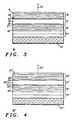
- FIG. 3illustrated in simplified sectional view is a complete VCSEL device according to the present invention. Illustrated is VCSEL 50 fabricated according to the disclosed method of the present invention.
- wafer structure 10 of FIG. 1is metal to metal wafer fused with wafer structure 40 of FIG. 2. More particularly, wafer structure 10 is flip mounted onto wafer structure 40 to allow for the fusing of heat dissipation layer 30 of FIG. 1 and heat dissipation layer 44 of FIG. 2. Once fused, the two separately formed heat dissipation layers become one heat dissipation layer 54 positioned adjacent substrate 42.
- the gallium arsenide substrate 12is removed by chemical etching. Buffer layer 14 and etch stop layer 16 are also removed during this process. Accordingly, a standard VCSEL epi structure is left remaining that includes heat dissipation layer 54 for high power operation.
- an electrical contact(not shown) is coupled to a surface of active region 21.
- a second electrical contact(not shown) is coupled to heat dissipation layer 54.
- Light 52is emitted from VCSEL 50 in a direction opposite substrate 42.
- FIG. 4all components similar to the components illustrated in FIG. 3, are designated with similar numbers, having a prime added to indicate the different embodiment. To the extent that such modifications and variations do not depart from the scope of the invention, they are intended to be included within the scope thereof which is assessed only by a fair interpretation of the following claims.
Landscapes
- Physics & Mathematics (AREA)
- Condensed Matter Physics & Semiconductors (AREA)
- General Physics & Mathematics (AREA)
- Electromagnetism (AREA)
- Optics & Photonics (AREA)
- Semiconductor Lasers (AREA)
Description
- This invention relates to vertical cavity surfaceemitting lasers and more specifically to vertical cavitysurface emitting lasers for high power operation.
- Vertical cavity surface emitting lasers (VCSEL) includea first distributed Bragg reflector (DBR), also referred toas a mirror stack, formed on top of a substrate bysemiconductor manufacturing techniques, an active regionformed on top of the first mirror stack, and a second mirrorstack formed on top of the active region. The VCSEL isdriven by current forced through the active region,typically achieved by providing a first contact on thereverse side of the substrate and a second contact on top ofthe second mirror stack.
- The use of mirror stacks in VCSELs is well establishedin the art. Typically, mirror stacks are formed of multiplepairs of layers often referred to as mirror pairs. Thepairs of layers are formed of a material system generallyconsisting of two materials having different indices of refraction and being easily lattice matched to the other portionsof the VCSEL. For example, a GaAs based VCSEL typically uses anAlx1Ga1-x1As\Alx2Ga1-x2As material system wherein the differentrefractive index of each layer of a pair is achieved by alteringthe aluminum content x1 and x2 in the layers. In conventionaldevices, the number of mirror pairs per stack may range from 20-40pairs to achieve a high percentage of reflectivity, dependingon the difference between the refractive indices of the layers.The large number of pairs increases the percentage of reflectedlight.
- In conventional VCSELs, conventional material systemsperform adequately. Such a VCSEL is disclosed in US-5146465,where the aluminum gallium nitride laser has an active regionthat is composed of aluminum gallium nitride material, and abuffer layer that is composed of aluminum nitride. However, newproducts are being developed, such as CD write devices and thoseutilizing infra-red data links, that require VCSELs to operate ata higher power, i.e. greater than 20 milliwatts. For example, inconventional 780 nm and 850 nm VCSELs, which utilize a GaAssubstrate, the GaAs substrate is absorptive with a laseremission being toward the opposite direction, the top.Accordingly, heat is dissipated into the GaAs substrate. TheGaAs substrate is not a good thermal conductor and thereby causesthe heat to accumulate near the active region. This in turn causes a temperature rise which saturates the laser output power.Therefore, it becomes difficult to generate high power from thistype of VCSEL, especially at ambient temperatures, i.e. 50-60 °C.
- Thus, there is a need for developing a reliable, stableand cost effective vertical cavity surface emitting laser (VCSEL) for use in high power operations, that includessmaller thermal resistance through the integration of a heatdissipator, thereby enabling the VCSEL to operate at highpower.
- It would be highly advantageous, therefore, to remedythe foregoing and other deficiencies inherent in the priorart. Accordingly, it is an object of the present inventionto provide a new and improved VCSEL for use in high poweroperations.
- Another object of the invention is to provide areliable high power VCSEL.
- And another object of the immediate invention is toprovide for an efficient heat dissipator for use in a highpower VCSEL.
- Still another object of the invention is to provide fora smaller degree of thermal resistance in a high powerVCSEL.
- Yet another object of the invention is to provide for ahighly manufacturable high power VCSEL.
- Briefly, to achieve the desired objects of the instantinvention in accordance with a preferred embodiment thereof,provided is a VCSEL for use in high power operation. TheVCSEL, as defined in Claims 1-9, generally includes a silicon substrate made from Si or SiC, a heatdissipation layer, a first stack of distributed Bragg reflectors, an active region, and a second stack ofdistributed Bragg reflectors.
- In a preferred embodiment the heat dissipation layer iscomposed of a gold germanium (AuGe) or a gold (Au) materialto efficiently dissipate heat from the active region intothe silicon substrate made from Si or SiC.
- The foregoing and further and more specific objects andadvantages of the instant invention will become readilyapparent to those skilled in the art from the followingdetailed description of a preferred embodiment thereof takenin conjunction with the drawings, in which:
- FIG. 1 is a sectional view of a first VCSEL waferstructure in accordance with the present invention;
- FIG. 2 is a sectional view of a second VCSEL waferstructure in accordance with the present invention;
- FIG. 3 is a complete VCSEL structure in accordance withthe present invention; and
- FIG. 4 is a complete VCSEL structure in accordance witha further embodiment of the present invention.
- Turning now to the drawings in which like referencecharacters indicate corresponding elements throughout theseveral views, attention is first directed to FIG. 1 whichillustrates the fabrication of a first vertical cavitysurface emitting laser (VCSEL) wafer structure generallydesignated 10.
Wafer structure 10 is formed on asubstrate 12, which in this specific embodiment is gallium arsenide(GaAs). GaAs is preferably used to facilitate latticematching of the components ofwafer structure 10 which emitsinfrared wavelength light, more particularly 780nm or 850nmlight, dependent upon the specific material system used.Also, GaAs is utilized so as to facilitate epitaxial growthof subsequent multiple layers that composewafer structure 10. It should be understood that GaAs is only utilized asan example and other semiconductor materials may be employedassubstrate 12, such as silicon (Si), indium phosphide(InP), or the like. - Typically, any suitable epitaxial deposition method,such as molecular beam epitaxy (MBE), metal organicchemical vapor deposition (MOCVD), or the like is used tomake the required multiple layers for
wafer structure 10.These methods allow for the epitaxial deposition ofmaterial layers, such as aluminum gallium arsenide,aluminum arsenide, indium aluminum gallium phosphide,gallium arsenide, and aluminum arsenide, or aluminumgallium phosphide, indium aluminum phosphide, and the like. It should be understood that epitaxial depositionis used extensively to produce the multitude of layersthat comprise the complete VCSEL device of the presentinvention. Substrate 12 has anupper surface 13 on which abufferlayer 14 is disposed.Buffer layer 14 includes a p-dopedgallium arsenide (GaAs) material. Next, anetch stop layer 16 is disposed onbuffer layer 14. Etchstop layer 16includes an aluminum gallium arsenide (AlGaAs) material oran aluminum gallium phosphide (AlGaP) material.Bufferlayer 14 andetch stop layer 16 will aid in the removal ofsubstrate 12 during the fabrication of the complete VCSELfor high power operation of the present invention.- A
first mirror stack 18 is disposed onetch stop layer 16. Anactive region 21 is disposed onmirror stack 18.Active region 21 includes anactive structure 22 sandwichedbetween afirst cladding region 23 adjacentfirst mirrorstack 18 and asecond cladding region 24. Asecond mirrorstack 26 is disposed on secondcladding region 24. - Referring now to distributed Bragg
reflectors reflector 18 is deposited first with subsequent deposition definingcladding region 23,active structure 22,cladding region 24,distributed Braggreflector 26 and aheat dissipation layer 30. Generally, thicknesses ofalternating layers alternating layers - Generally, doping of the distributed Bragg
reflectors reflector 18 and a portion ofcladding region 23 are P-typed doped,with a portion ofcladding region 23,active structure 22,and a portion ofcladding region 24 being undoped, and witha portion ofcladding region 24, and distributed Braggreflector 26 being N-typed doped. - In the present invention, distributed Bragg
reflectors layers layers alternating layers etch stop layer 16 and layers 27and 28 are epitaxially disposed or deposited on oroverlayingcladding region 24, thereby generatingdistributedBragg reflectors Mirror stack match mirror stack 18 to substrate 12 asuitable semiconductor material system must be deposited.Approximately 20-40 mirror pairs of this material system aredeposited onetch stop layer 16 depending on the difference between the refractive indices of the layers. As will beexplained presently, doping the mirror stacks is notnecessary since electrical contacts to the active region canbe made laterally.- For the sake of simplicity and to prevent overcrowdingof the figure,
cladding region 23 is shown as a singlelayer; however, it should be understood that claddingregion 23 is made of at least two components that are epitaxiallydisposed or deposited on distributedBragg reflector 18.First, a layer of any suitable material such as aluminumgallium arsenide (AlGaAs) having an appropriate thicknessand being doped similarly to distributedBragg reflector 18is epitaxially deposited on distributedBragg reflector 18. - By way of example, an n-doped aluminum gallium arsenidelayer (Al.60Ga.40As) is epitaxially deposited on distributed
Bragg reflector 18. Generally, the AlGaAs layer has athickness that is determined by the wavelength of light thatis to be emitted from the VCSEL structure, thereby allowingthe thickness of the AlGaAs layer to be any suitablethickness. Second, a layer of any suitable material havingan appropriate thickness is epitaxially deposited on thefirst layer of thecladding region 23. - For the sake of simplicity,
active structure 22 isrepresented by a single layer which is epitaxially depositedor disposed oncladding region 23; however, it should beunderstood that theactive structure 22 can include multiplelayers of barrier regions with quantum well regionsinterspersed. By way of a simple example,active structure 22 is made of at least two barrier layers and a quantum wellregion with the quantum well region being positioned betweenthe two barrier regions. In a preferred embodiment,activestructure 22 is made of four barrier regions and threequantum well regions with the quantum well region beingpositioned between the two barrier regions. In a VCSELstructure that emits at 780 nm, the quantum well region(s)is made of undoped aluminum gallium arsenide (Al.12Ga.88As)and the barrier regions are made of aluminum galliumarsenide (Al.30Ga.70As). In a VCSEL structure that emits at850nm, the quantum well region(s) is made of undoped galliumarsenide (GaAs) and the barrier regions are made of aluminumgallium arsenide (Al.30Ga.70As). Typically,active structure 22 includes three to five quantum wells with theircorresponding barrier regions. One skilled in the art willunderstand that more or fewer quantum well layers andbarrier layers can be used depending upon the application.Active region 21 and first and second mirror stacks 18 and26 respectively are configured to emit light with awavelength of approximately 780nm or 850nm. - For the sake of simplicity and to prevent overcrowdingof the figure,
cladding region 24 is shown as a singlelayer; however, it should be understood that claddingregion 24 is made of two components that are disposed or depositedepitaxially onactive structure 22. First, a layer of anysuitable undoped cladding material is epitaxially depositedto an appropriate thickness onactive structure 22. Second, a layer of any suitable doped cladding material isepitaxially deposed on the undoped cladding material. - By way of example, an undoped aluminum gallium arsenide(Al.60Ga.40As) layer is epitaxially deposited on
activestructure 22. Generally, the undoped AlGaAs has a thicknessthat is determined by the wavelength of light that is to beemitted from the VCSEL device, thereby allowing thethickness of the AlGaAs layer to be any suitable thickness.Subsequently, a doped layer is epitaxially deposited on theundoped layer. The doped layer is generally doped with a n-typedopant. - A
heat dissipation layer 30 is formed by disposinglayers of any suitable material on distributedBraggreflector 26, such as nickel (Ni), gold germanium (AuGe),gold (Au), chromium (Cr), zinc gold (ZnAu), titaniumtungsten (TiW), titanium gold (TiAu), or the like. Itshould be understood that depending upon which materialselection is made the specific method of disposing andpatterning of that specific material will change to formheat dissipation layer 30. In addition, material selectionis dependent upon the doping oftop DBR 26 ofwaferstructure 10. For example, whentop DBR 26 is n-type doped,heat dissipation layer 30 includes layers of nickel (Ni),gold germanium (AuGe), and gold (Au). Whentop DBR 26 is p-typedoped,heat dissipation layer 30 includes layers ofchromium (Cr), zinc gold (ZnAu), and gold (Au),or titaniumtungsten (TiW) and gold (Au), or titanium gold (TiAu) andgold (Au). With the inclusion of an alloy,heat dissipation layer 30 further serves as an electrical contact for thecompleted VCSEL device. - Referring now to FIG. 2, a
second wafer structure 40 isfabricated as a part of the VCSEL device of the presentinvention.Second wafer structure 40 includes asubstrate 42.Substrate 42 in this example is made of any suitablematerial, such as silicon (Si), silicon carbide (SiC ), orthe like. Next, aheat dissipation layer 44 is epitaxiallydeposited on an upper surface 43 ofsubstrate 42.Heatdissipation layer 44 is formed by disposing any suitablematerial on distributedBragg reflector 26, such as gold(Au), or the like. It should be understood that dependingupon which material selection is made the specific method ofdisposing and patterning of that specific material willchange to formheat dissipation layer 30. - Referring now to FIG. 3, illustrated in simplifiedsectional view is a complete VCSEL device according to thepresent invention. Illustrated is
VCSEL 50 fabricatedaccording to the disclosed method of the present invention.During fabrication,wafer structure 10 of FIG. 1 is metal tometal wafer fused withwafer structure 40 of FIG. 2. Moreparticularly,wafer structure 10 is flip mounted ontowaferstructure 40 to allow for the fusing ofheat dissipationlayer 30 of FIG. 1 andheat dissipation layer 44 of FIG. 2.Once fused, the two separately formed heat dissipationlayers become oneheat dissipation layer 54 positionedadjacent substrate 42. - Next, the
gallium arsenide substrate 12 is removed bychemical etching.Buffer layer 14 andetch stop layer 16are also removed during this process. Accordingly, astandard VCSEL epi structure is left remaining that includesheat dissipation layer 54 for high power operation. - To complete
VCSEL 50, an electrical contact (not shown)is coupled to a surface ofactive region 21. A secondelectrical contact (not shown) is coupled toheatdissipation layer 54.Light 52 is emitted fromVCSEL 50 in adirection oppositesubstrate 42. Various changes andmodifications to the embodiments herein chosen for purposesof illustration will readily occur to those skilled in theart. For example, it should be understood that VCSELstructure symmetry exists for both the p and n dopants aswell as electrically inverted structure designs asillustrated in FIG. 4. It should be noted that in FIG. 4all components similar to the components illustrated in FIG.3, are designated with similar numbers, having a prime addedto indicate the different embodiment. To the extent thatsuch modifications and variations do not depart from thescope of the invention, they are intended to be includedwithin the scope thereof which is assessed only by a fairinterpretation of the following claims. - The various steps of the method disclosed have beenperformed in a specific order for purposes of explanation,however, it should be understood that various steps of thedisclosed method may be interchanged and/or combined withother steps in specific applications and it is fully intended that all such changes in the disclosed methods comewithin the scope of the claims.
- While we have shown and described specific embodimentsof the present invention, further modifications andimprovement will occur to those skilled in the art. Wedesire it to be understood, therefore, that this inventionis not limited to the particular forms shown and we intendin the appended claims to cover all modifications that donot depart from the scope of this invention.
Claims (9)
- A vertical cavity surface emitting laser, comprising:a substrate (42) having a surface and being made from silicon (Si) or siliconcarbide (SiC);a heat dissipation layer (30, 44, 54) disposed on the surface of the substrate, theheat dissipation layer including layers of one of a chromium material, a zinc gold (ZnAu)material and a gold (Au) material, or a titanium tungsten (TiW) material and a gold (Au)material, or a titanium gold (TiAu) material and a gold (Au) material, or combinationsthereof, or layers of one of nickel (Ni) or gold germanium (AuGe) or gold (Au);a first mirror stack (26) disposed on the heat dissipation layer (30, 44, 54);an active region (21) disposed on the first mirror stack (26) the active regionincluding gallium arsenide; anda second mirror stack (18) disposed on the active region (21).
- A vertical cavity surface emitting laser as claimed in claim 1 furthercharacterized in that the laser is configured for high power operation of greater than 20milliwatts.
- A vertical cavity surface emitting laser as claimed in claim 1 furthercharacterized in that the active region (21) and the first and second mirror stacks (26,18) are configured to emit light with a wavelength of approximately 780 nm.
- A vertical cavity surface emitting laser as claimed in claim 1 furthercharacterized in that the active region (21) and the first and the second mirror stacks(26, 18) are configured to emit light with a wavelength of approximately 850 nm.
- A vertical cavity surface emitting laser as claimed in claim1 furthercharacterized in that the heat dissipation layer (30, 44, 54) includes two separate heatdissipation layers (30, 44), fused together during the fabrication process of the verticalcavity surface emitting laser, thereby forming a single heat dissipation layer (54).
- A vertical cavity surface emitting laser as claimed in claim 1 furthercharacterized in that the first mirror stack (26) and the second mirror stack (18) eachinclude a plurality of pairs (19/20, 27/28) of alternating layers of an Alx1Ga1-x1 As/Alx2Ga1-x2 As material system.
- A vertical cavity surface emitting laser as claimed in claim 1 furthercharacterized in that the first mirror stack (26) includes a plurality of pairs of (27/28) ofalternating layer of a Alx1Ga1-x1 As/Alx2Ga1-x2 material and the second mirror stack (18)includes a plurality of pairs (19/20) of alternating layers of a dielectric material.
- A method of fabricating a vertical cavity surface emitting laser, comprising thesteps of:providing a first wafer structure (10) including a substrate (12) having a surface(13), a buffer layer (14) disposed on the surface (13), an etch stop layer (16) disposedon the buffer layer (14), a mirror stack (18) disposed on the etch stop layer 916), anactive region (21) disposed on the mirror stack (18), an additional mirror stack (26)disposed on the active region (21) and a heat dissipation layer (30) disposed on theadditional mirror stack (26);providing a second wafer structure (40) including a substrate (42) a substrate(42) having a surface and being made from silicon (Si) or silicon carbide (SiC) and aheat dissipation layer (44) disposed on the surface of the substrate (42)whereby theheat dissipation layer includes layers of one of a chromium material, a zinc gold (ZnAu)material and a gold (Au) material, or a titanium tungsten (TiW) material and a gold (Au)material, or a titanium gold (TiAu) material and a gold (Au) material, or combinationsthereof, or layers of one of nickel (Ni) or gold germanium (AuGe) or gold (Au);flip mounting the first wafer structure (10) to the second wafer structure (40),fusing the heat dissipation layer (30) of the first wafer structure (10) to the heatdissipation layer (44) of the second wafer structure (40);removing the substrate (12), the buffer layer (14) and the etch stop layer (16)from the first wafer structure (10); andforming a first and a second electrical contact in electrical cooperation with theactive region.
- A vertical cavity surface emitting laser as claimed in claims 1 to 7 obtainableby the method of claim 8.
Applications Claiming Priority (2)
| Application Number | Priority Date | Filing Date | Title |
|---|---|---|---|
| US795260 | 1997-02-10 | ||
| US08/795,260US5914973A (en) | 1997-02-10 | 1997-02-10 | Vertical cavity surface emitting laser for high power operation and method of fabrication |
Publications (3)
| Publication Number | Publication Date |
|---|---|
| EP0860915A2 EP0860915A2 (en) | 1998-08-26 |
| EP0860915A3 EP0860915A3 (en) | 1999-03-17 |
| EP0860915B1true EP0860915B1 (en) | 2003-04-23 |
Family
ID=25165131
Family Applications (1)
| Application Number | Title | Priority Date | Filing Date |
|---|---|---|---|
| EP98102181AExpired - LifetimeEP0860915B1 (en) | 1997-02-10 | 1998-02-09 | Vertical cavity surface emitting laser for high power operation and method of fabrication |
Country Status (5)
| Country | Link |
|---|---|
| US (1) | US5914973A (en) |
| EP (1) | EP0860915B1 (en) |
| JP (1) | JPH10256654A (en) |
| DE (1) | DE69813655T2 (en) |
| TW (1) | TW363293B (en) |
Families Citing this family (21)
| Publication number | Priority date | Publication date | Assignee | Title |
|---|---|---|---|---|
| US6160830A (en) | 1998-03-04 | 2000-12-12 | Motorola, Inc. | Semiconductor laser device and method of manufacture |
| US6577658B1 (en) | 1999-09-20 | 2003-06-10 | E20 Corporation, Inc. | Method and apparatus for planar index guided vertical cavity surface emitting lasers |
| US6621842B1 (en) | 1999-10-15 | 2003-09-16 | E20 Communications, Inc. | Method and apparatus for long wavelength semiconductor lasers |
| NL1015714C2 (en)* | 2000-07-14 | 2002-01-15 | Dsm Nv | Process for crystallizing enantiomerically enriched 2-acetylthio-3-phenylpropanoic acid. |
| US6628685B1 (en)* | 2000-08-21 | 2003-09-30 | Chan-Long Shieh | Method of fabricating long-wavelength VCSEL and apparatus |
| US6810064B1 (en)* | 2000-08-22 | 2004-10-26 | The Regents Of The University Of California | Heat spreading layers for vertical cavity surface emitting lasers |
| US6905900B1 (en)* | 2000-11-28 | 2005-06-14 | Finisar Corporation | Versatile method and system for single mode VCSELs |
| US6657237B2 (en)* | 2000-12-18 | 2003-12-02 | Samsung Electro-Mechanics Co., Ltd. | GaN based group III-V nitride semiconductor light-emitting diode and method for fabricating the same |
| JP4676100B2 (en)* | 2001-08-07 | 2011-04-27 | 古河電気工業株式会社 | Epitaxial growth method of Al-containing compound semiconductor layer |
| US6782019B2 (en)* | 2001-08-16 | 2004-08-24 | Applied Optoelectronics, Inc. | VCSEL with heat-spreading layer |
| DE10147888A1 (en) | 2001-09-28 | 2003-04-24 | Osram Opto Semiconductors Gmbh | Optically pumped vertically emitting semiconductor laser |
| US8257393B2 (en)* | 2003-12-04 | 2012-09-04 | Ethicon, Inc. | Active suture for the delivery of therapeutic fluids |
| US20050190810A1 (en)* | 2004-02-27 | 2005-09-01 | Stuart Butterworth | Contact-bonded optically pumped semiconductor laser structure |
| KR100627703B1 (en)* | 2004-12-14 | 2006-09-26 | 한국전자통신연구원 | Hybrid metal bonded surface emitting laser and its manufacturing method |
| KR20070027232A (en)* | 2005-09-06 | 2007-03-09 | 삼성전자주식회사 | Post-Pumped Vertical External Resonant Surface Emitting Laser |
| TWI303473B (en)* | 2005-12-12 | 2008-11-21 | High Power Optoelectronics Inc | Semiconductor device integrated with heat sink and method of fabricating the same |
| JP2010285581A (en)* | 2009-06-15 | 2010-12-24 | Toyota Motor Corp | Insulating resin composition |
| TWM392637U (en) | 2010-07-01 | 2010-11-21 | Three In One Ent Co Ltd | A portable otoscope |
| TWM392638U (en) | 2010-07-01 | 2010-11-21 | Three In One Ent Co Ltd | A portable otoscope with a detachable screen |
| CN111180995A (en)* | 2019-11-19 | 2020-05-19 | 浙江博升光电科技有限公司 | Substrate transfer vertical cavity surface emitting laser and method of manufacturing the same |
| CN114094440B (en)* | 2021-10-22 | 2024-03-26 | 南京邮电大学 | GaN base surface emitting laser based on film overturning process and preparation method |
Family Cites Families (5)
| Publication number | Priority date | Publication date | Assignee | Title |
|---|---|---|---|---|
| US5063569A (en)* | 1990-12-19 | 1991-11-05 | At&T Bell Laboratories | Vertical-cavity surface-emitting laser with non-epitaxial multilayered dielectric reflectors located on both surfaces |
| US5146465A (en)* | 1991-02-01 | 1992-09-08 | Apa Optics, Inc. | Aluminum gallium nitride laser |
| US5384795A (en)* | 1992-09-15 | 1995-01-24 | Texas Instruments Incorporated | Light emission from rare-earth element-doped CaF2 thin films by electroluminescence |
| US5422901A (en)* | 1993-11-15 | 1995-06-06 | Motorola, Inc. | Semiconductor device with high heat conductivity |
| US5724376A (en)* | 1995-11-30 | 1998-03-03 | Hewlett-Packard Company | Transparent substrate vertical cavity surface emitting lasers fabricated by semiconductor wafer bonding |
- 1997
- 1997-02-10USUS08/795,260patent/US5914973A/ennot_activeExpired - Lifetime
- 1998
- 1998-02-09DEDE69813655Tpatent/DE69813655T2/ennot_activeExpired - Lifetime
- 1998-02-09EPEP98102181Apatent/EP0860915B1/ennot_activeExpired - Lifetime
- 1998-02-10TWTW087101797Apatent/TW363293B/ennot_activeIP Right Cessation
- 1998-02-10JPJP10046204Apatent/JPH10256654A/enactivePending
Also Published As
| Publication number | Publication date |
|---|---|
| DE69813655T2 (en) | 2003-11-06 |
| EP0860915A3 (en) | 1999-03-17 |
| JPH10256654A (en) | 1998-09-25 |
| TW363293B (en) | 1999-07-01 |
| EP0860915A2 (en) | 1998-08-26 |
| DE69813655D1 (en) | 2003-05-28 |
| US5914973A (en) | 1999-06-22 |
Similar Documents
| Publication | Publication Date | Title |
|---|---|---|
| EP0860915B1 (en) | Vertical cavity surface emitting laser for high power operation and method of fabrication | |
| US5903586A (en) | Long wavelength vertical cavity surface emitting laser | |
| US6021147A (en) | Vertical cavity surface emitting laser for high power single mode operation and method of fabrication | |
| US5966399A (en) | Vertical cavity surface emitting laser with integrated diffractive lens and method of fabrication | |
| US7491565B2 (en) | III-nitride light emitting devices fabricated by substrate removal | |
| US6026111A (en) | Vertical cavity surface emitting laser device having an extended cavity | |
| US5978398A (en) | Long wavelength vertical cavity surface emitting laser | |
| US6061380A (en) | Vertical cavity surface emitting laser with doped active region and method of fabrication | |
| JP5063869B2 (en) | Vertical cavity surface emitting laser with high thermal conductivity | |
| US5943359A (en) | Long wavelength VCSEL | |
| US6720585B1 (en) | Low thermal impedance DBR for optoelectronic devices | |
| US5903590A (en) | Vertical-cavity surface-emitting laser device | |
| US5706306A (en) | VCSEL with distributed Bragg reflectors for visible light | |
| US5963576A (en) | Annular waveguide vertical cavity surface emitting laser and method of fabrication | |
| US9014225B2 (en) | Vertical cavity surface emitting laser device | |
| US5392307A (en) | Vertical optoelectronic semiconductor device | |
| US5883912A (en) | Long wavelength VCSEL | |
| WO2002017445A1 (en) | Heat spreading layers for vertical cavity surface emitting lasers | |
| JP2002299742A (en) | Vertical cavity surface emitting laser, method of manufacturing the same, and communication system | |
| US6021146A (en) | Vertical cavity surface emitting laser for high power single mode operation and method of fabrication | |
| EP1298461A1 (en) | Distributed Bragg reflector comprising GaP and a semiconductor resonant cavity device comprising such DBR | |
| EP0860916B1 (en) | Long wavelength VCSEL | |
| US6931044B2 (en) | Method and apparatus for improving temperature performance for GaAsSb/GaAs devices | |
| US5956364A (en) | Vertical cavity surface emitting laser with shaped cavity mirror and method of fabrication | |
| US6008067A (en) | Fabrication of visible wavelength vertical cavity surface emitting laser |
Legal Events
| Date | Code | Title | Description |
|---|---|---|---|
| PUAI | Public reference made under article 153(3) epc to a published international application that has entered the european phase | Free format text:ORIGINAL CODE: 0009012 | |
| AK | Designated contracting states | Kind code of ref document:A2 Designated state(s):DE FR GB | |
| AX | Request for extension of the european patent | Free format text:AL;LT;LV;MK;RO;SI | |
| PUAL | Search report despatched | Free format text:ORIGINAL CODE: 0009013 | |
| AK | Designated contracting states | Kind code of ref document:A3 Designated state(s):AT BE CH DE DK ES FI FR GB GR IE IT LI LU MC NL PT SE | |
| AX | Request for extension of the european patent | Free format text:AL;LT;LV;MK;RO;SI | |
| 17P | Request for examination filed | Effective date:19990917 | |
| AKX | Designation fees paid | Free format text:DE FR GB | |
| 17Q | First examination report despatched | Effective date:20010315 | |
| GRAH | Despatch of communication of intention to grant a patent | Free format text:ORIGINAL CODE: EPIDOS IGRA | |
| RIC1 | Information provided on ipc code assigned before grant | Free format text:7H 01S 5/183 A, 7H 01S 5/024 B | |
| RIC1 | Information provided on ipc code assigned before grant | Free format text:7H 01S 5/183 A, 7H 01S 5/024 B | |
| GRAH | Despatch of communication of intention to grant a patent | Free format text:ORIGINAL CODE: EPIDOS IGRA | |
| GRAA | (expected) grant | Free format text:ORIGINAL CODE: 0009210 | |
| AK | Designated contracting states | Designated state(s):DE FR GB | |
| REG | Reference to a national code | Ref country code:GB Ref legal event code:FG4D | |
| REF | Corresponds to: | Ref document number:69813655 Country of ref document:DE Date of ref document:20030528 Kind code of ref document:P | |
| ET | Fr: translation filed | ||
| PLBE | No opposition filed within time limit | Free format text:ORIGINAL CODE: 0009261 | |
| STAA | Information on the status of an ep patent application or granted ep patent | Free format text:STATUS: NO OPPOSITION FILED WITHIN TIME LIMIT | |
| 26N | No opposition filed | Effective date:20040126 | |
| REG | Reference to a national code | Ref country code:GB Ref legal event code:732E | |
| REG | Reference to a national code | Ref country code:GB Ref legal event code:732E | |
| REG | Reference to a national code | Ref country code:FR Ref legal event code:TP | |
| REG | Reference to a national code | Ref country code:FR Ref legal event code:PLFP Year of fee payment:18 | |
| PGFP | Annual fee paid to national office [announced via postgrant information from national office to epo] | Ref country code:DE Payment date:20150226 Year of fee payment:18 | |
| PGFP | Annual fee paid to national office [announced via postgrant information from national office to epo] | Ref country code:FR Payment date:20150217 Year of fee payment:18 Ref country code:GB Payment date:20150226 Year of fee payment:18 | |
| REG | Reference to a national code | Ref country code:DE Ref legal event code:R119 Ref document number:69813655 Country of ref document:DE | |
| GBPC | Gb: european patent ceased through non-payment of renewal fee | Effective date:20160209 | |
| REG | Reference to a national code | Ref country code:FR Ref legal event code:ST Effective date:20161028 | |
| PG25 | Lapsed in a contracting state [announced via postgrant information from national office to epo] | Ref country code:GB Free format text:LAPSE BECAUSE OF NON-PAYMENT OF DUE FEES Effective date:20160209 Ref country code:FR Free format text:LAPSE BECAUSE OF NON-PAYMENT OF DUE FEES Effective date:20160229 Ref country code:DE Free format text:LAPSE BECAUSE OF NON-PAYMENT OF DUE FEES Effective date:20160901 |