EP0851485B1 - Self-aligned etching process to realize word lines of semiconductor integrated memory devices - Google Patents
Self-aligned etching process to realize word lines of semiconductor integrated memory devicesDownload PDFInfo
- Publication number
- EP0851485B1 EP0851485B1EP96830649AEP96830649AEP0851485B1EP 0851485 B1EP0851485 B1EP 0851485B1EP 96830649 AEP96830649 AEP 96830649AEP 96830649 AEP96830649 AEP 96830649AEP 0851485 B1EP0851485 B1EP 0851485B1
- Authority
- EP
- European Patent Office
- Prior art keywords
- layer
- self
- conducting layer
- etching process
- aligned etching
- Prior art date
- Legal status (The legal status is an assumption and is not a legal conclusion. Google has not performed a legal analysis and makes no representation as to the accuracy of the status listed.)
- Expired - Lifetime
Links
- 238000005530etchingMethods0.000titleclaimsdescription44
- 238000000034methodMethods0.000titleclaimsdescription33
- 239000004065semiconductorSubstances0.000titleclaimsdescription18
- 239000000758substrateSubstances0.000claimsdescription15
- 238000012876topographyMethods0.000claimsdescription12
- 229910021420polycrystalline siliconInorganic materials0.000claimsdescription9
- 229920005591polysiliconPolymers0.000claimsdescription9
- 230000008021depositionEffects0.000claimsdescription6
- 229910021332silicideInorganic materials0.000claimsdescription3
- FVBUAEGBCNSCDD-UHFFFAOYSA-Nsilicide(4-)Chemical compound[Si-4]FVBUAEGBCNSCDD-UHFFFAOYSA-N0.000claimsdescription3
- WQJQOUPTWCFRMM-UHFFFAOYSA-Ntungsten disilicideChemical compound[Si]#[W]#[Si]WQJQOUPTWCFRMM-UHFFFAOYSA-N0.000claimsdescription3
- 229910021342tungsten silicideInorganic materials0.000claimsdescription3
- 229910008814WSi2Inorganic materials0.000claimsdescription2
- 238000000151depositionMethods0.000claims2
- 239000000126substanceSubstances0.000claims1
- 239000010410layerSubstances0.000description56
- 230000015654memoryEffects0.000description16
- 238000009413insulationMethods0.000description5
- 238000000206photolithographyMethods0.000description5
- 239000011159matrix materialSubstances0.000description4
- 230000001681protective effectEffects0.000description3
- 239000004020conductorSubstances0.000description2
- 230000000875corresponding effectEffects0.000description2
- 230000003647oxidationEffects0.000description2
- 238000007254oxidation reactionMethods0.000description2
- 238000004458analytical methodMethods0.000description1
- 230000015572biosynthetic processEffects0.000description1
- 230000002596correlated effectEffects0.000description1
- 239000002019doping agentSubstances0.000description1
- 230000000694effectsEffects0.000description1
- 238000004519manufacturing processMethods0.000description1
- 239000000463materialSubstances0.000description1
- 238000000386microscopyMethods0.000description1
- 229920000642polymerPolymers0.000description1
- 239000011241protective layerSubstances0.000description1
- 238000007789sealingMethods0.000description1
Images

Classifications
- H—ELECTRICITY
- H10—SEMICONDUCTOR DEVICES; ELECTRIC SOLID-STATE DEVICES NOT OTHERWISE PROVIDED FOR
- H10B—ELECTRONIC MEMORY DEVICES
- H10B41/00—Electrically erasable-and-programmable ROM [EEPROM] devices comprising floating gates
- H10B41/30—Electrically erasable-and-programmable ROM [EEPROM] devices comprising floating gates characterised by the memory core region
- H—ELECTRICITY
- H01—ELECTRIC ELEMENTS
- H01L—SEMICONDUCTOR DEVICES NOT COVERED BY CLASS H10
- H01L21/00—Processes or apparatus adapted for the manufacture or treatment of semiconductor or solid state devices or of parts thereof
- H01L21/02—Manufacture or treatment of semiconductor devices or of parts thereof
- H01L21/04—Manufacture or treatment of semiconductor devices or of parts thereof the devices having potential barriers, e.g. a PN junction, depletion layer or carrier concentration layer
- H01L21/18—Manufacture or treatment of semiconductor devices or of parts thereof the devices having potential barriers, e.g. a PN junction, depletion layer or carrier concentration layer the devices having semiconductor bodies comprising elements of Group IV of the Periodic Table or AIIIBV compounds with or without impurities, e.g. doping materials
- H01L21/30—Treatment of semiconductor bodies using processes or apparatus not provided for in groups H01L21/20 - H01L21/26
- H01L21/31—Treatment of semiconductor bodies using processes or apparatus not provided for in groups H01L21/20 - H01L21/26 to form insulating layers thereon, e.g. for masking or by using photolithographic techniques; After treatment of these layers; Selection of materials for these layers
- H01L21/3205—Deposition of non-insulating-, e.g. conductive- or resistive-, layers on insulating layers; After-treatment of these layers
- H01L21/321—After treatment
- H01L21/3213—Physical or chemical etching of the layers, e.g. to produce a patterned layer from a pre-deposited extensive layer
- H—ELECTRICITY
- H01—ELECTRIC ELEMENTS
- H01L—SEMICONDUCTOR DEVICES NOT COVERED BY CLASS H10
- H01L21/00—Processes or apparatus adapted for the manufacture or treatment of semiconductor or solid state devices or of parts thereof
- H01L21/70—Manufacture or treatment of devices consisting of a plurality of solid state components formed in or on a common substrate or of parts thereof; Manufacture of integrated circuit devices or of parts thereof
- H01L21/71—Manufacture of specific parts of devices defined in group H01L21/70
- H01L21/768—Applying interconnections to be used for carrying current between separate components within a device comprising conductors and dielectrics
- H01L21/76838—Applying interconnections to be used for carrying current between separate components within a device comprising conductors and dielectrics characterised by the formation and the after-treatment of the conductors
Definitions
- the present inventionrelates to a self-aligned etching process for providing word lines in electronic memory devices integrated on semiconductor substrates displaying a topography of the matrix type comprising word lines and bit lines.
- the present inventionrelates to a self-aligned etching process for providing a plurality of parallel word lines in a first conducting layer deposited over a planarized architecture obtained starting from a semiconductor substrate on which is provided a plurality of active elements extending along separate parallel lines e.g. bit lines for memory cells comprising gate regions formed by a first conducting layer, an intermediate dielectric layer and a second conducting layer, said regions being insulated from each other by insulation regions to form this architecture with said word lines being defined photolithographically by protective strips.
- bit lines for memory cellscomprising gate regions formed by a first conducting layer, an intermediate dielectric layer and a second conducting layer, said regions being insulated from each other by insulation regions to form this architecture with said word lines being defined photolithographically by protective strips.
- the present inventionalso relates to a memory device with matrix configuration of the cross-point type and comprising bit lines and word lines.
- the present inventionconcerns specifically but not exclusively a self-aligned etching process for providing word lines in contactless semiconductor memories having a virtual ground circuitry.
- the following descriptionis given with reference to this specific field of application with the only purpose of simplifying its explanation.
- EPROM or FLASH-EPROM electronic memory devicesrequire the provision on a semiconductor substrate of a matrix-type topography in which a plurality of bit lines having a floating gate region is intersected on the top by a plurality of conducting strips properly called word lines.
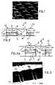
- FIG 1A typical topography of this type is shown in the photograph of FIG 1 obtained by electronic microscopy techniques.
- a thin gate oxide layer 3is deposited.
- a deposition of a first polysilicon layer 4, identified by the name POLY1is provided.
- a deposition of a second dielectric interpoly layer 5follows, e.g. ONO, such an interpoly layer is encapsulated on the top by another layer 6 of polysilicon which is identified by the name POLYCAP.
- a masked photolithography stepwhich for convenience is identified by the name 'POLY1 mask' defines the topography of the gate regions and related bit lines.
- a self-aligned etchingallows removal of parallel strips of multiple layers until reaching the active areas of the substrate 1.
- This etching phaseremoves from the unprotected areas of the photolithography the POLYCAP layer 6, the ONO layer 5, the POLY1 layer 4, the gate oxide layer 3 and the field oxide 2 if necessary where present.
- the gate regions 13are formed as shown in FIG 2 by the stratified structure of POLYCAP - ONO - POLY1 - gate oxide and field oxide if any.
- removal of the POLYCAP layer 6causes the deposition of polymers which create a pair of steps 10 or ribs on the underlying POLY1 layer 4, which thus projects laterally with respect to the layers deposited above as shown in FIGS 2 and 4.
- Another cause which could be at the origin of the formation of this pair of steps 10is generally an additional oxidation step usually used for sealing the gate regions 13.
- the POLYCAP layer 6can reoxidize more than the POLY1 layer 4 (depending on the type of dopant in POLY1) as shown in FIG 2.
- step 10 formed by the POLY1 layer 4 projecting laterallycan originate a short circuit between adjacent floating gate regions once a self-aligned etching has been completed to define word lines and hence individual memory cells.
- FIG 3shows an electronic microscope photograph of a semiconductor substrate having a matrix-type topography after performance of a self-aligned etching to define the word lines, which can be identified in the high-luminosity areas which are connected by thin white strips revealing the presence of the steps 10.
- Provision of the plurality of word lines intersecting the gate regions 13calls for the deposition of a conducting layer entirely covering the planarized architecture 9 as shown in FIG 4.
- This conducting layercan be obtained by means of successive deposition of a protective layer 12, e.g. of polysilicon and indicated for convenience by the name POLY2, and a final layer 11 of silicide, e.g. tungsten silicide.
- a protective layer 12e.g. of polysilicon and indicated for convenience by the name POLY2
- a final layer 11 of silicidee.g. tungsten silicide.
- Another objective of this etchingis to mutually insulate the individual memory cells by removing material from the floating gate regions unprotected by the photolithography step.
- the first stepcalls for removal of the conducting layer 11, 12 and the underlying POLYCAP layer 6 while the second step calls for removal of the ONO layer 5 and POLY1 layer 4.
- the prior art process described up to nowhas provided on the semiconductor substrate 1 a matrix topography comprising gate regions 13, corresponding bit lines and word lines orthogonal thereto.
- This topographyis widely used in EPROM or E 2 PROM memory devices and in particular in EPROM, Flash EPROM and EEPROM memory devices having a cross-point and virtual ground structure as described e.g. in European patent no. 0 573 728.
- the technical problem underlying the present inventionis to conceive a self-aligned etching process for definition of geometry associated with word lines which would allow overcoming the above mentioned shortcomings which still limit the reliability of the memory devices provided in accordance with the prior art.
- the solution idea underlying the present inventionis that of using, for the definition of the word lines and individual memory cells, a self-aligned etching with a vertical profile limited to removal of the conducting layer and the underlying Polycap and interpoly layers 6 and 5.
- FIG 1shows an electronic microscope photograph of a plurality of Flash EPROM memory cells having a matrix-type topography of which can be seen only the bit lines,
- FIGS 2 and 2Ashow diagrammatically and in enlarged scale a vertical cross section of a semiconductor electronic device with a planarized architecture comprising gate regions conformed as a stratified POLYCAP - ONO - POLY1 - gate oxide structure, with the possible presence of field oxide in FIG 2A,
- FIG 3shows an electronic microscope photograph of a semiconductor substrate having a matrix-type topography and taken after performance of a self-aligned etching for definition of the word lines
- FIGS 4 and 4Ashow schematically and in enlarged scale with the possible presence of field oxide in FIG 4A a vertical cross section of a semiconductor electronic device with a planarized architecture covered above by a conducting layer provided in accordance with the prior art, and
- FIGS 5 and 5Ashow schematically and in enlarged scale with the possible presence of field oxide in FIG 5A a vertical cross-section of a semiconductor electronic device limited to a gate region conformed as a stratified POLY2 - POLYCAP - ONO - POLY1 structure created by a process in accordance with the present invention after etching performed with a so-called POLY2 mask.
- These layers 11, 12are deposited over a planarized architecture 9 obtained starting from a semiconductor substrate 1 on which a plurality of active elements is provided extending along separated parallel lines, e.g. bit lines of memory cells.
- These memory cellscomprise gate regions 13 made up of a thin gate oxide layer 3, a first conducting layer 4, an intermediate dielectric layer 5 and a second conducting layer 6.
- the gate regions 13are mutually insulated by insulating regions 7, 8 forming said planarized architecture 9.
- the word linesare defined photolithographically by protective strips which are orthogonal to the bit lines.
- FIG 5In the example of FIG 5 is illustrated the vertical cross section of a floating gate region following provision of a self-aligned etching in accordance with the principles of the present invention.
- the vertical cross section of the floating gate regionshows a stratified structure built over a semiconductor substrate 1 and comprising an optional field oxide layer 2, a thin gate oxide layer 3, a first polysilicon conducting layer 4 indicated as POLY1, an interpoly dielectric layer 5 e.g. ONO, and a second conducting polysilicon layer 6 indicated as POLYCAP.
- a first polysilicon conducting layer 4indicated as POLY1
- an interpoly dielectric layer 5e.g. ONO
- POLYCAPsecond conducting polysilicon layer 6 indicated as POLYCAP.
- POLYCAPOver the POLYCAP layer 6 is provided another conducting layer including two layers 12, 11, i.e. the first 12 of polysilicon termed also POLY2 and the second 11 of silicide e.g. tungsten silicide (WSi 2 ).
- the etching for definition of the word line geometry and insulation of the individual memory cellsis provided in two successive steps.
- a self-aligned etchingstarting from the exposed surface of the additional conducting layer 11, 12.
- This etchingproceeds with a vertical profile for removal of the conducting layer 11, 12 and of the underlying layers 6 and 5 of POLYCAP and ONO from the gate regions 13 not protected by the photolithographic process.
- a POLY2 maskis used for definition of the word lines in the photolithography step.
- This isotropic etchingcan extend its action even laterally so as to remove also the pair of polysilicon steps 10 formed as fully explained with reference to the prior art.
- FIG 5the vertical cross section of the individual cell taken from the floating gate region 13 shows a characteristic morphology easily identifiable by means of a SEM, TEM or FIB analysis.
- the self-aligned etching proposed by the present inventionis capable of ensuring good reliability of the memory devices with matrix configuration if provided in accordance with the process steps described here.
Landscapes
- Engineering & Computer Science (AREA)
- Physics & Mathematics (AREA)
- Condensed Matter Physics & Semiconductors (AREA)
- General Physics & Mathematics (AREA)
- Manufacturing & Machinery (AREA)
- Computer Hardware Design (AREA)
- Microelectronics & Electronic Packaging (AREA)
- Power Engineering (AREA)
- Non-Volatile Memory (AREA)
- Semiconductor Memories (AREA)
- Drying Of Semiconductors (AREA)
Description
- The present invention relates to a self-aligned etching process for providing word lines in electronic memory devices integrated on semiconductor substrates displaying a topography of the matrix type comprising word lines and bit lines.
- Specifically the present invention relates to a self-aligned etching process for providing a plurality of parallel word lines in a first conducting layer deposited over a planarized architecture obtained starting from a semiconductor substrate on which is provided a plurality of active elements extending along separate parallel lines e.g. bit lines for memory cells comprising gate regions formed by a first conducting layer, an intermediate dielectric layer and a second conducting layer, said regions being insulated from each other by insulation regions to form this architecture with said word lines being defined photolithographically by protective strips.
- The present invention also relates to a memory device with matrix configuration of the cross-point type and comprising bit lines and word lines.
- The present invention concerns specifically but not exclusively a self-aligned etching process for providing word lines in contactless semiconductor memories having a virtual ground circuitry. The following description is given with reference to this specific field of application with the only purpose of simplifying its explanation.
- As is well known, EPROM or FLASH-EPROM electronic memory devices require the provision on a semiconductor substrate of a matrix-type topography in which a plurality of bit lines having a floating gate region is intersected on the top by a plurality of conducting strips properly called word lines.
- A typical topography of this type is shown in the photograph of FIG 1 obtained by electronic microscopy techniques.
- The practical provision of this matrix-type topography is not entirely without problems and shortcomings because it was verified experimentally that it is possible that the floating gate regions find themselves contacted by spurious residues of conducting materials not entirely removed during manufacturing.
- In the following description given by way of example there are again proposed the process steps necessary for defining on a semiconductor substrate a matrix-type topography of an EPROM memory device comprising word lines, bit lines and floating gate regions to better clarify those aspects which are necessary for defining the technical problem.
- Starting from a
semiconductor substrate 1, e.g. like the one shown in FIG 2, in which a division into active areas with the possible presence of a field oxide dividinglayer 2 is already provided, multiple deposits are made over the entire surface of the substrate. - Firstly a thin
gate oxide layer 3 is deposited. Then a deposition of afirst polysilicon layer 4, identified by the name POLY1, is provided. A deposition of a seconddielectric interpoly layer 5 follows, e.g. ONO, such an interpoly layer is encapsulated on the top by anotherlayer 6 of polysilicon which is identified by the name POLYCAP. - At this point a masked photolithography step which for convenience is identified by the name 'POLY1 mask' defines the topography of the gate regions and related bit lines.
- A self-aligned etching allows removal of parallel strips of multiple layers until reaching the active areas of the
substrate 1. - This etching phase removes from the unprotected areas of the photolithography the POLYCAP
layer 6, theONO layer 5, thePOLY1 layer 4, thegate oxide layer 3 and thefield oxide 2 if necessary where present. - This defines a spatial geometry on the
semiconductor substrate 1 in which it is possible to recognize a plurality of active elements extending along separate parallel lines, e.g. memory cell bit lines andcorresponding gate regions 13. - The
gate regions 13 are formed as shown in FIG 2 by the stratified structure of POLYCAP - ONO - POLY1 - gate oxide and field oxide if any. - During performance of this self-aligned etching, removal of the
POLYCAP layer 6 causes the deposition of polymers which create a pair ofsteps 10 or ribs on theunderlying POLY1 layer 4, which thus projects laterally with respect to the layers deposited above as shown in FIGS 2 and 4. - Another cause which could be at the origin of the formation of this pair of
steps 10 is generally an additional oxidation step usually used for sealing thegate regions 13. During this oxidation step thePOLYCAP layer 6 can reoxidize more than the POLY1 layer 4 (depending on the type of dopant in POLY1) as shown in FIG 2. - The above mentioned
step 10 formed by thePOLY1 layer 4 projecting laterally can originate a short circuit between adjacent floating gate regions once a self-aligned etching has been completed to define word lines and hence individual memory cells. - FIG 3 shows an electronic microscope photograph of a semiconductor substrate having a matrix-type topography after performance of a self-aligned etching to define the word lines, which can be identified in the high-luminosity areas which are connected by thin white strips revealing the presence of the
steps 10. - The successive process steps for the provision of an EPROM memory device call for the use of a planarization method in which a first insulating
dielectric film 8 and a second planarizingdielectric film 7; both films are deposited in the interstitial regions delimited by thegate regions 13 and allow obtaining a planarized architecture 9 as shown in FIG 2. - It is important to note that the above described process causes the first insulating
dielectric film 8 to act as a protective micromask for thestep 10 created previously. - Provision of the plurality of word lines intersecting the
gate regions 13 calls for the deposition of a conducting layer entirely covering the planarized architecture 9 as shown in FIG 4. - This conducting layer can be obtained by means of successive deposition of a
protective layer 12, e.g. of polysilicon and indicated for convenience by the name POLY2, and afinal layer 11 of silicide, e.g. tungsten silicide. - To define the spatial geometry of the word lines there is again made use of a conventional photolithography step with an appropriate mask usually indicated as a POLY2 mask designating unprotected areas in which a self-aligned etching can be performed even for the word lines.
- Another objective of this etching is to mutually insulate the individual memory cells by removing material from the floating gate regions unprotected by the photolithography step.
- Those skilled in the art usually perform this self-aligned etching in two successive steps and with a vertical profile.
- The first step calls for removal of the conducting
layer layer 6 while the second step calls for removal of theONO layer 5 andPOLY1 layer 4. - The prior art process described up to now has provided on the semiconductor substrate 1 a matrix topography comprising
gate regions 13, corresponding bit lines and word lines orthogonal thereto. This topography is widely used in EPROM or E2PROM memory devices and in particular in EPROM, Flash EPROM and EEPROM memory devices having a cross-point and virtual ground structure as described e.g. in European patent no. 0 573 728. - Although meeting the purpose, there are some critical aspects of the above described process which require a remedy.
- In particular it is desired to place the accent on the existence of the pair of
steps 10 present in the floating gate regions associated with each bit line between the POLYCAPlayer 5 and the underlying layers. As mentioned, these steps can originate undesired contacts which can affect the reliability of the memory device. - In addition, the usual self-aligned etchings having a vertical profile for definition of the word lines as well as for insulation of the individual memory cells are quite inadequate for removing
said steps 10 as may be seen in FIG 3. - Indeed, it happens that after removal of the
ONO layer 5 andPOLY1 layer 4 the pairs ofsteps 10 still remain present because protected by the micromask created by the firstdielectric insulation film 8 used for planarization of the architecture 9. - In this manner the floating gate regions of adjacent memory cells made by means of self-aligned etching of the word lines come into mutual electrical contact.
- The technical problem underlying the present invention is to conceive a self-aligned etching process for definition of geometry associated with word lines which would allow overcoming the above mentioned shortcomings which still limit the reliability of the memory devices provided in accordance with the prior art.
- The US patent No. 5,342,801 to Perry et al. describes a manufaturing method of memory cells comprising an isotropic etching phase to suppress stringers in such memory cells.
- In this document no indication is given of a process involving a polycap layer and of the problems, related to its etching.
- The solution idea underlying the present invention is that of using, for the definition of the word lines and individual memory cells, a self-aligned etching with a vertical profile limited to removal of the conducting layer and the underlying Polycap and
interpoly layers - Subsequent removal of the
POLY1 layer 4 necessary for insulation of the individual memory cells is provided by means of an isotropic etching. - On the basis of this solution idea the technical problem is solved by a process of the type indicated above and defined in the characterizing part of
claim 1. - The characteristics and advantages of the process in accordance with the present invention are set forth in the description of an embodiment thereof given below by way of non-limiting example with reference to the annexed drawings.
- FIG 1 shows an electronic microscope photograph of a plurality of Flash EPROM memory cells having a matrix-type topography of which can be seen only the bit lines,
- FIGS 2 and 2A show diagrammatically and in enlarged scale a vertical cross section of a semiconductor electronic device with a planarized architecture comprising gate regions conformed as a stratified POLYCAP - ONO - POLY1 - gate oxide structure, with the possible presence of field oxide in FIG 2A,
- FIG 3 shows an electronic microscope photograph of a semiconductor substrate having a matrix-type topography and taken after performance of a self-aligned etching for definition of the word lines,
- FIGS 4 and 4A show schematically and in enlarged scale with the possible presence of field oxide in FIG 4A a vertical cross section of a semiconductor electronic device with a planarized architecture covered above by a conducting layer provided in accordance with the prior art, and
- FIGS 5 and 5A show schematically and in enlarged scale with the possible presence of field oxide in FIG 5A a vertical cross-section of a semiconductor electronic device limited to a gate region conformed as a stratified POLY2 - POLYCAP - ONO - POLY1 structure created by a process in accordance with the present invention after etching performed with a so-called POLY2 mask.
- With reference to the above FIGS there is now described a self-aligned etching process for providing a plurality of mutually parallel word lines in a first conducting layer made up of a pair of
superimposed layers - These
layers semiconductor substrate 1 on which a plurality of active elements is provided extending along separated parallel lines, e.g. bit lines of memory cells. - These memory cells comprise
gate regions 13 made up of a thingate oxide layer 3, a first conductinglayer 4, an intermediatedielectric layer 5 and a second conductinglayer 6. Thegate regions 13 are mutually insulated by insulatingregions - The word lines are defined photolithographically by protective strips which are orthogonal to the bit lines.
- In the example of FIG 5 is illustrated the vertical cross section of a floating gate region following provision of a self-aligned etching in accordance with the principles of the present invention.
- The vertical cross section of the floating gate region shows a stratified structure built over a
semiconductor substrate 1 and comprising an optionalfield oxide layer 2, a thingate oxide layer 3, a first polysilicon conductinglayer 4 indicated as POLY1, an interpolydielectric layer 5 e.g. ONO, and a second conductingpolysilicon layer 6 indicated as POLYCAP. Over the POLYCAPlayer 6 is provided another conducting layer including twolayers - Advantageously in accordance with the present invention the etching for definition of the word line geometry and insulation of the individual memory cells is provided in two successive steps.
- In a first step there is provided the action of a self-aligned etching starting from the exposed surface of the
additional conducting layer layer underlying layers gate regions 13 not protected by the photolithographic process. As mentioned above, a POLY2 mask is used for definition of the word lines in the photolithography step. - In the second step of the process in accordance with the present invention the use of an isotropic etching is called for for removal of the
POLY1 layer 4 from the floatinggate regions 13. - This isotropic etching can extend its action even laterally so as to remove also the pair of polysilicon steps 10 formed as fully explained with reference to the prior art.
- The repeatability and effectiveness of the process proposed is well correlated with the choice of an isotropic etching time sufficient to remove the pair of steps.
- The effect secured by employing this type of etching in this process step is clearly visible in FIG 5 in which the vertical cross section of the individual cell taken from the floating
gate region 13 shows a characteristic morphology easily identifiable by means of a SEM, TEM or FIB analysis. - Indeed, there can be seen a typical undercut of the
POLY1 layer 4 linked to the use of the isotropic etching in the second process step. - One of ordinary skill in the art will surely recognize in the process proposed here a solution to all those technical problems in which there is conducting material previously not removed because protected by undesired micromasks which can cause spurious contacts.
- It is noted in particular that the technical problem set forth above and concerning the possibility of spurious contacts between the floating gate regions associated with adjacent memory cells remains even when the profile of the vertical cross section of the
gate regions 13 is the trapezoid type and not only in the presence of a step as described. - In conclusion the self-aligned etching proposed by the present invention is capable of ensuring good reliability of the memory devices with matrix configuration if provided in accordance with the process steps described here.
Claims (7)
- Self-aligned etching process for providing a plurality of mutually parallel word lines in a first conducting layer (11,12) deposited over a planarized architecture (9) obtained starting from a semiconductor substrate (1) said process comprising the following steps:- forming on the semiconductor substrate (1) a thin dielectric layer (3), a second conducting layer (4), an intermediate dielectric layer (5) and a third conducting layer (6),- forming a first mask layer on said third conducting layer (6) in order to define the topography of gate regions and related bit lines,- self-aligned etching from the unprotected areas of said third conducting layer (6), said intermediate dielectric layer (5), said second conducting layer (4) and said thin dielectric layer (3) in order to provider separate parallel lines whereby by the removal of said third conducting layer (6) steps (10) are formed on said second conducting layer (4),- depositing a planarizing dielectric film (7, 8) in order to obtain said planarized architecture (9);- forming said first conductive layer (11, 12) on said planarized architecture (9),- forming a second mask on said first conducting layer (11, 12),characterized by the following steps :- a vertical profile etching for complete removal from the unprotected areas of the first conducting layers (11,12), of the third conducting layer (6) and of the intermediate dielectric layer (5) respectively and- a following isotropic etching of the second conducting layer (4), said isotropic etching extending its action laterally so to remove said steps (10), said isotropic etching being performed for a time sufficient to remove said steps (10).
- Self-aligned etching process in accordance with claim 1 andcharacterized in that said first conducting layer (11,12) can be provided by means of successive depositions of a first (12) and a second (11) layer having different chemical composition.
- Self-aligned etching process in accordance with claim 2 andcharacterized in that said first layer (12) is polysilicon.
- Self-aligned etching process in accordance with claim 2 andcharacterized in that the second layer (11) is silicide.
- Self-aligned etching process in accordance with claim 4 andcharacterized in that the second layer (11) is a tungsten silicide (WSi2).
- Self-aligned etching process in accordance with claim 1 andcharacterized in that said second conducting layer (4) and said third conducting layer (6) making up the gate regions are polysilicon.
- Self-aligned etching process in accordance with claim 1 andcharacterized in that said intermediate dielectric layer (5) is interpoly ONO.
Priority Applications (5)
| Application Number | Priority Date | Filing Date | Title |
|---|---|---|---|
| DE69637095TDE69637095D1 (en) | 1996-12-24 | 1996-12-24 | Self-aligned etching method for realizing the word lines of integrated semiconductor memory devices |
| EP96830649AEP0851485B1 (en) | 1996-12-24 | 1996-12-24 | Self-aligned etching process to realize word lines of semiconductor integrated memory devices |
| JP9348835AJPH10261777A (en) | 1996-12-24 | 1997-12-18 | Self-aligned type etching process for realizing word line of memory device integrated on semiconductor substrate |
| US08/997,499US6130165A (en) | 1996-12-24 | 1997-12-23 | Autoaligned etching process for realizing word lines in memory devices integrated semiconductor substrates |
| US09/528,406US6380582B2 (en) | 1996-12-24 | 2000-03-17 | Autoaligned etching process for realizing word lines in memory devices integrated semiconductor substrates |
Applications Claiming Priority (1)
| Application Number | Priority Date | Filing Date | Title |
|---|---|---|---|
| EP96830649AEP0851485B1 (en) | 1996-12-24 | 1996-12-24 | Self-aligned etching process to realize word lines of semiconductor integrated memory devices |
Publications (2)
| Publication Number | Publication Date |
|---|---|
| EP0851485A1 EP0851485A1 (en) | 1998-07-01 |
| EP0851485B1true EP0851485B1 (en) | 2007-05-23 |
Family
ID=8226092
Family Applications (1)
| Application Number | Title | Priority Date | Filing Date |
|---|---|---|---|
| EP96830649AExpired - LifetimeEP0851485B1 (en) | 1996-12-24 | 1996-12-24 | Self-aligned etching process to realize word lines of semiconductor integrated memory devices |
Country Status (4)
| Country | Link |
|---|---|
| US (2) | US6130165A (en) |
| EP (1) | EP0851485B1 (en) |
| JP (1) | JPH10261777A (en) |
| DE (1) | DE69637095D1 (en) |
Families Citing this family (4)
| Publication number | Priority date | Publication date | Assignee | Title |
|---|---|---|---|---|
| KR100311049B1 (en)* | 1999-12-13 | 2001-10-12 | 윤종용 | Nonvolatile semiconductor memory device and manufacturing method thereof |
| JP2003309194A (en)* | 2002-04-18 | 2003-10-31 | Nec Electronics Corp | Semiconductor storage device and its manufacturing method |
| US20040113648A1 (en)* | 2002-12-13 | 2004-06-17 | Wen-Jyh Hung | Method of exposing desired layers in a multi-layer semiconductor using focused ion beams for physical failure |
| CN100418210C (en)* | 2004-09-22 | 2008-09-10 | 中芯国际集成电路制造(上海)有限公司 | Levelling method of multilayer laminated polycrystalline silicon grid for flash storage |
Family Cites Families (9)
| Publication number | Priority date | Publication date | Assignee | Title |
|---|---|---|---|---|
| US5296396A (en)* | 1988-12-05 | 1994-03-22 | Sgs-Thomson Microelectronics S.R.L. | Matrix of EPROM memory cells with a tablecloth structure having an improved capacitative ratio and a process for its manufacture |
| IT1236980B (en)* | 1989-12-22 | 1993-05-12 | Sgs Thomson Microelectronics | NON-VOLATILE EPROM MEMORY CELL WITH DIVIDED GATE AND SELF-ALIGNED FIELD INSULATION PROCESS FOR OBTAINING THE ABOVE CELL |
| US5160407A (en)* | 1991-01-02 | 1992-11-03 | Applied Materials, Inc. | Low pressure anisotropic etch process for tantalum silicide or titanium silicide layer formed over polysilicon layer deposited on silicon oxide layer on semiconductor wafer |
| US5240870A (en)* | 1991-04-18 | 1993-08-31 | National Semiconductor Corporation | Stacked gate process flow for cross-point EPROM with internal access transistor |
| JP2723396B2 (en)* | 1991-09-19 | 1998-03-09 | シャープ株式会社 | Method of manufacturing nonvolatile memory device |
| EP0573728B1 (en)* | 1992-06-01 | 1996-01-03 | STMicroelectronics S.r.l. | Process for fabricating high density contactless EPROMs |
| US5342801A (en)* | 1993-03-08 | 1994-08-30 | National Semiconductor Corporation | Controllable isotropic plasma etching technique for the suppression of stringers in memory cells |
| US5629230A (en)* | 1995-08-01 | 1997-05-13 | Micron Technology, Inc. | Semiconductor processing method of forming field oxide regions on a semiconductor substrate utilizing a laterally outward projecting foot portion |
| US5847427A (en)* | 1995-12-21 | 1998-12-08 | Kabushiki Kaisha Toshiba | Non-volatile semiconductor memory device utilizing an oxidation suppressing substance to prevent the formation of bird's breaks |
- 1996
- 1996-12-24EPEP96830649Apatent/EP0851485B1/ennot_activeExpired - Lifetime
- 1996-12-24DEDE69637095Tpatent/DE69637095D1/ennot_activeExpired - Lifetime
- 1997
- 1997-12-18JPJP9348835Apatent/JPH10261777A/enactivePending
- 1997-12-23USUS08/997,499patent/US6130165A/ennot_activeExpired - Lifetime
- 2000
- 2000-03-17USUS09/528,406patent/US6380582B2/ennot_activeExpired - Lifetime
Non-Patent Citations (1)
| Title |
|---|
| None* |
Also Published As
| Publication number | Publication date |
|---|---|
| US20020014653A1 (en) | 2002-02-07 |
| JPH10261777A (en) | 1998-09-29 |
| US6380582B2 (en) | 2002-04-30 |
| US6130165A (en) | 2000-10-10 |
| EP0851485A1 (en) | 1998-07-01 |
| DE69637095D1 (en) | 2007-07-05 |
Similar Documents
| Publication | Publication Date | Title |
|---|---|---|
| US6784481B2 (en) | Flash memory device with isolation regions and a charge storage dielectric layer formed only on an active region | |
| US7579244B2 (en) | Method of fabricating a semiconductor device | |
| US6677639B2 (en) | Non-volatile memory device and method for fabricating the same | |
| US6362050B2 (en) | Method for forming a non-volatile memory cell that eliminates substrate trenching | |
| EP0851485B1 (en) | Self-aligned etching process to realize word lines of semiconductor integrated memory devices | |
| KR20040023716A (en) | Method of manufacturing a semiconductor device with a non-volatile memory comprising a memory cell with an access gate and with a control gate and a charge storage region | |
| US6034395A (en) | Semiconductor device having a reduced height floating gate | |
| US5639681A (en) | Process for eliminating effect of polysilicon stringers in semiconductor devices | |
| US20070207556A1 (en) | Manufacturing method of non-volatile memory | |
| EP0851484B1 (en) | Self-aligned etching process to realize word lines of semiconductor integrated memory devices | |
| EP1032035B1 (en) | Process of manufacturing electronic virtual ground memory devices | |
| US20030092237A1 (en) | Process for manufacturing non-volatile memory cells integrated on a semiconductor substrate | |
| US6365456B1 (en) | Process for manufacturing semiconductor integrated memory devices with cells matrix having virtual ground | |
| JP2008166325A (en) | Method of manufacturing semiconductor device | |
| CN1591879A (en) | EEPROM and its mfg. method | |
| TWI796160B (en) | Memory device and method of manufacturing the same | |
| US6228723B1 (en) | Method for forming split gate non-volatile memory cells without forming a conductive layer on a boundary region between a memory cell array and peripheral logic | |
| KR20050002424A (en) | Method of manufacturing flash memory device | |
| EP0902463A1 (en) | Method for forming a plurality of parallel floating gate regions by avoiding poly stringers formation | |
| JPH06338597A (en) | Method for formation of buried bit-line array of memory cell | |
| CN116867271A (en) | Memory element and method for manufacturing the same | |
| US20070026610A1 (en) | Sealing method for electronic devices formed on a common semiconductor substrate and corresponding circuit structure | |
| JP2000200839A (en) | Semiconductor storage device and method of manufacturing the same | |
| JPH10144890A (en) | Non-volatile semiconductor memory device | |
| KR19990088353A (en) | Method of forming non-volatile semiconductor memory |
Legal Events
| Date | Code | Title | Description |
|---|---|---|---|
| PUAI | Public reference made under article 153(3) epc to a published international application that has entered the european phase | Free format text:ORIGINAL CODE: 0009012 | |
| AK | Designated contracting states | Kind code of ref document:A1 Designated state(s):DE FR GB IT | |
| AX | Request for extension of the european patent | Free format text:AL;LT;LV;RO;SI | |
| RAP3 | Party data changed (applicant data changed or rights of an application transferred) | Owner name:STMICROELECTRONICS S.R.L. | |
| 17P | Request for examination filed | Effective date:19981221 | |
| AKX | Designation fees paid | Free format text:DE FR GB IT | |
| RBV | Designated contracting states (corrected) | Designated state(s):DE FR GB IT | |
| 17Q | First examination report despatched | Effective date:20030819 | |
| GRAP | Despatch of communication of intention to grant a patent | Free format text:ORIGINAL CODE: EPIDOSNIGR1 | |
| GRAC | Information related to communication of intention to grant a patent modified | Free format text:ORIGINAL CODE: EPIDOSCIGR1 | |
| GRAS | Grant fee paid | Free format text:ORIGINAL CODE: EPIDOSNIGR3 | |
| GRAA | (expected) grant | Free format text:ORIGINAL CODE: 0009210 | |
| AK | Designated contracting states | Kind code of ref document:B1 Designated state(s):DE FR GB IT | |
| REG | Reference to a national code | Ref country code:GB Ref legal event code:FG4D | |
| REF | Corresponds to: | Ref document number:69637095 Country of ref document:DE Date of ref document:20070705 Kind code of ref document:P | |
| ET | Fr: translation filed | ||
| PGFP | Annual fee paid to national office [announced via postgrant information from national office to epo] | Ref country code:IT Payment date:20071211 Year of fee payment:12 | |
| PLBE | No opposition filed within time limit | Free format text:ORIGINAL CODE: 0009261 | |
| STAA | Information on the status of an ep patent application or granted ep patent | Free format text:STATUS: NO OPPOSITION FILED WITHIN TIME LIMIT | |
| 26N | No opposition filed | Effective date:20080226 | |
| PG25 | Lapsed in a contracting state [announced via postgrant information from national office to epo] | Ref country code:DE Free format text:LAPSE BECAUSE OF FAILURE TO SUBMIT A TRANSLATION OF THE DESCRIPTION OR TO PAY THE FEE WITHIN THE PRESCRIBED TIME-LIMIT Effective date:20070824 | |
| PGFP | Annual fee paid to national office [announced via postgrant information from national office to epo] | Ref country code:GB Payment date:20081125 Year of fee payment:13 | |
| PGFP | Annual fee paid to national office [announced via postgrant information from national office to epo] | Ref country code:FR Payment date:20081224 Year of fee payment:13 | |
| GBPC | Gb: european patent ceased through non-payment of renewal fee | Effective date:20091224 | |
| REG | Reference to a national code | Ref country code:FR Ref legal event code:ST Effective date:20100831 | |
| PG25 | Lapsed in a contracting state [announced via postgrant information from national office to epo] | Ref country code:FR Free format text:LAPSE BECAUSE OF NON-PAYMENT OF DUE FEES Effective date:20091231 | |
| PG25 | Lapsed in a contracting state [announced via postgrant information from national office to epo] | Ref country code:GB Free format text:LAPSE BECAUSE OF NON-PAYMENT OF DUE FEES Effective date:20091224 | |
| PG25 | Lapsed in a contracting state [announced via postgrant information from national office to epo] | Ref country code:IT Free format text:LAPSE BECAUSE OF NON-PAYMENT OF DUE FEES Effective date:20081224 |