EP0851442A2 - Lead-in insulator - Google Patents
Lead-in insulatorDownload PDFInfo
- Publication number
- EP0851442A2 EP0851442A2EP97660151AEP97660151AEP0851442A2EP 0851442 A2EP0851442 A2EP 0851442A2EP 97660151 AEP97660151 AEP 97660151AEP 97660151 AEP97660151 AEP 97660151AEP 0851442 A2EP0851442 A2EP 0851442A2
- Authority
- EP
- European Patent Office
- Prior art keywords
- insulator
- lead
- measuring element
- voltage
- voltage measuring
- Prior art date
- Legal status (The legal status is an assumption and is not a legal conclusion. Google has not performed a legal analysis and makes no representation as to the accuracy of the status listed.)
- Granted
Links
Images
Classifications
- G—PHYSICS
- G01—MEASURING; TESTING
- G01R—MEASURING ELECTRIC VARIABLES; MEASURING MAGNETIC VARIABLES
- G01R15/00—Details of measuring arrangements of the types provided for in groups G01R17/00 - G01R29/00, G01R33/00 - G01R33/26 or G01R35/00
- G01R15/14—Adaptations providing voltage or current isolation, e.g. for high-voltage or high-current networks
- G01R15/142—Arrangements for simultaneous measurements of several parameters employing techniques covered by groups G01R15/14 - G01R15/26
- G—PHYSICS
- G01—MEASURING; TESTING
- G01R—MEASURING ELECTRIC VARIABLES; MEASURING MAGNETIC VARIABLES
- G01R15/00—Details of measuring arrangements of the types provided for in groups G01R17/00 - G01R29/00, G01R33/00 - G01R33/26 or G01R35/00
- G01R15/14—Adaptations providing voltage or current isolation, e.g. for high-voltage or high-current networks
- G01R15/18—Adaptations providing voltage or current isolation, e.g. for high-voltage or high-current networks using inductive devices, e.g. transformers
- G01R15/181—Adaptations providing voltage or current isolation, e.g. for high-voltage or high-current networks using inductive devices, e.g. transformers using coils without a magnetic core, e.g. Rogowski coils
- H—ELECTRICITY
- H01—ELECTRIC ELEMENTS
- H01F—MAGNETS; INDUCTANCES; TRANSFORMERS; SELECTION OF MATERIALS FOR THEIR MAGNETIC PROPERTIES
- H01F38/00—Adaptations of transformers or inductances for specific applications or functions
- H01F38/20—Instruments transformers
- H01F38/22—Instruments transformers for single phase AC
- H01F38/34—Combined voltage and current transformers
- H01F38/36—Constructions
Definitions
- the present inventionrelates to a lead-in insulator comprising a primary conductor centrally led through the body of the insulator, a current measuring element arranged around the primary conductor, and a voltage measuring element, based on voltage division and arranged inside the current measuring element concentrically therewith.
- Lead-in insulatorsaccording to the preamble are known e.g. from US patent publications 4,074,193 and 5,272,460.
- the current and voltage measuring sensorsare integrated into a nested apparatus, the current measuring sensor acting as a disturbance shield around the voltage measuring element.
- Thisprovides a relatively accurate voltage measurement which at least to some extent tolerates the disturbance fields effective around the insulator.
- apparatuses and railsit is vitally important to know if the apparatus or rail is live in order for maintenance to be carried out absolutely safely.
- the insulators known from the above referencesdo not, in addition to said voltage measuring element, comprise other elements enabling voltage detection, and consequently it is not possible to achieve a sufficient reliability level with these insulators without separate devices suitable for voltage detection.
- the lead-in insulators known from said referenceshave a straight body. Typically only one downwards extending cable can be connected to a straight lead-in insulator. If more parallel cables are to be connected to the lead-in, the apparatuses and rails have to be subjected to a structurally expensive arrangement by means of which the lead-in insulator can be positioned horizontally. Several downwards extending parallel cables can then be connected to such a horizontal lead-in insulator by means of T-branch cable terminals.
- the lead-in insulator of the inventionis primarily characterized in that the insulator further comprises a second voltage measuring element for voltage detection, arranged substantially axially with respect to said voltage measuring element.
- the voltage measuring element of the insulatoris disposed concentrically inside the current measuring element.
- the most substantial structural advantageis that the current and voltage measuring elements require only a short axial space, whereby the body of the lead-in insulator and consequently the therein centrally traversing primary conductor can be bent into a desired angle, preferably an angle of substantially 90°, although the insulator is further provided with a voltage detection element, disposed axially with respect to the voltage measuring element. Because of the bending into an angle, several parallel cables can be coupled to the cable terminal by the use of T-branch cable terminals without having to place the lead-in insulator in a horizontal position.
- the basic idea of the insulator of the inventionis that the separation of voltage measuring from voltage detection ensures that a fault in the voltage measuring circuit does not result in an incorrect diagnosis regarding the presence of voltage.
- the lead-in insulator of the inventionenables the use of two such voltage measuring sensors, typically metal cylinders, since the current and voltage measuring sensors are nested.
- the nested disposition of the current measuring and voltage measuring elementsmay also be utilized electrotechnically such that the metal casing of the Rogowski sensor acting as the current measuring element, coupled to the ground potential, operates as the ground plane of the capacitive voltage measuring sensor.
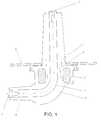
- FIG. 1shows a lead-in insulator of the invention to be mounted in an opening in a wall 12 of a medium voltage apparatus.
- the lead-in insulatorcomprises a body 5 of insulating material and a primary conductor 4 running centrally inside it. The ends of the primary conductor are provided with spiral bores 6 and 7 for connections to a cable and a conductor rail, respectively.
- the insulatorcomprises a cable terminal 8 of the type of an external cone to which the T-branch cable terminal at the end of the cable is secured.
- a plurality of such T-branch cable terminalscan be connected in parallel, allowing several cables to be connected by means of the same lead-in.
- the body 5 of the lead-in insulator and the primary conductor 4 arranged thereinform a substantially 90° angle to enable T-branch cable terminals of the type described above to be used in a lead-in insulator without having to place it in a horizontal position.
- the lead-in insulator of the inventionallows the use of conventional apparatus and rail structures, a possibility which does not exist when the lead-in insulator is disposed in a horizontal position. Consequently, the use of the lead-in insulator of the invention enables significantly simpler apparatus structures compared with other solutions enabling the connection of several cables to the same lead-in insulator.
- FIG. 1shows, three sensors are arranged inside the lead-in insulator of the invention, reference numeral 1 denoting a metal cylinder employed for voltage detection, reference numeral 2 denoting a metal cylinder employed for voltage measuring, and reference numeral 3 denoting a Rogowski sensor employed for current measuring. It is essential in the lead-in insulator of the invention that the metal cylinder 2 for voltage measuring and the Rogowski sensor 3 are nested. This reduces the axial length of the lead-in insulator enabling it to be turned into a 90° angle and also providing several electrotechnical advantages to the operation of the sensors.
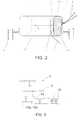
- FIG. 2shows in more detail the structures of the Rogowski sensor 3 and the metal cylinder 2 arranged therein and serving as the voltage measuring element.
- the Rogowski sensorcomprises a toroidal coil 9 around which is arranged a metal casing made of two halves 10a and 10b that can be partially nested. The electrical coupling of the halves is secured by a copper conductor 17. Since the cross section of the metal case of the Rogowski sensor must not form a closed loop, the halves 10a and 10b are separated from one another by an air gap 11 which in a finished lead-in insulator is filled with the insulating material of the lead-in insulator, such as cast resin.
- This gap 11forms a gap circulating around the inner periphery of the toroidal ring formed by the halves 10a and 10b and opposite which the metal cylinder 2 employed as the voltage measuring element is disposed.
- the purpose of placing the air gap of the toroidal metal casing of the Rogowski sensor on the inner periphery of the casing assemblyis to avoid external disturbances.
- Mounting bushings 13are also connected to the casing half 10a of the Rogowski sensor and serve to couple the entire lead-in insulator to the mounting opening in the wall 12 of the apparatus. These bushings also serve to ground the metal sheath of the Rogowski sensor. Reference numerals 14 denote coupling conductors to the coil 9 of the Rogowski sensor.
- the metal cylinder 2 serving as the voltage measuring element and based on capacitive voltage divisionis embodied in the Rogowski sensor.
- the metal case of the Rogowski sensoris coupled to the ground potential through mounting brackets 13 and serves as the ground plane for the capacitive voltage measuring sensor 2, whereby there is no need for a separate ground plane typical of a capacitive voltage measuring element. When grounded, the metal case 10a, 10b of the Rogowski sensor attenuates the disturbances caused in voltage measuring by external electric fields.
- Figure 3illustrates the electric coupling of the voltage measuring element 2, and, for the sake of clarity, the same reference numerals as in Figures 1 and 2 designate the different components of the measuring arrangement.
- Figure 3shows how a capacitive coupling is formed between the primary conductor and the metal cylinder 2 and between the voltage measuring cylinder 2 and the casing 10a, 10b of the Rogowski sensor.
- the measuring conductor connected to the voltage measuring element 2is denoted by the reference numeral 15.
- This conductoris a coaxial cable with a grounded sheath, as is apparent from the coupling of Figure 3.
- Figure 3further shows external capacitances 16, forming part of the capacitive measuring arrangement of the voltage measuring element.
- the metal cylinder 2 of the voltage measuring sensoralso provides an advantage in the operation of the Rogowski sensor by preventing the effect of the electric field of the primary conductor 4 directly on the coil 9 of the Rogowski sensor through the air gap 11 in its metal casing 10a, 10b.
- a second separate metal cylinder 1is also disposed for voltage detection around the primary conductor 4.
- the separation of voltage measuring and detectionensures that a fault in the voltage measuring circuit does not cause an erroneous diagnosis regarding the presence of voltage.
- the magnitude and stability of the capacitance generated between the primary conductor 4 and the metal cylinder 2 of the voltage measuring element and between the metal cylinder 2 and the metal casing serving as the ground planedepend on the material used as insulant.
- the most inexpensive methodis to cast the voltage measuring element 2 into the same cast resin as the rest of the structure, but it is possible to cast the measuring elements 2 and 3 first into a different material which is then cast inside normal cast resin in order to produce the lead-in insulator assembly of the invention.
Landscapes
- Engineering & Computer Science (AREA)
- Power Engineering (AREA)
- Physics & Mathematics (AREA)
- General Physics & Mathematics (AREA)
- Insulators (AREA)
- Measuring Instrument Details And Bridges, And Automatic Balancing Devices (AREA)
- Power Conversion In General (AREA)
- Emergency Protection Circuit Devices (AREA)
- Polymers With Sulfur, Phosphorus Or Metals In The Main Chain (AREA)
- Measurement Of Current Or Voltage (AREA)
Abstract
Description
Claims (4)
- A lead-in insulator comprising a primary conductor (4) centrallyled through the body (5) of the insulator, a current measuring element (3) arrangedaround the primary conductor, and a voltage measuring element (2),based on voltage division and arranged inside the current measuring element(3) concentrically therewith,characterized in that the insulator furthercomprises a second voltage measuring element (1) for voltage detection, arrangedsubstantially axially with respect to said voltage measuring element (2).
- A lead-in insulator as claimed in claim 1,characterized inthat the primary conductor (4) is bent into an angle, preferably an angle ofsubstantially 90°.
- A lead-in insulator as claimed in claim 1 or 2 when the currentmeasuring element is a Rogowski sensor (3) comprising a toroidal coil (9),characterized in that the coil (9) of the Rogowski sensor is embodiedby a toroidal metal case (10a, 10b) comprising a breakpoint or gap (11) circulatingaround the inner periphery opposite the metal cylinder (2) employed asthe voltage measuring element.
- A lead-in insulator as claimed in claim 3,characterized inthat the metal case (10a, 10b) of the Rogowski sensor (3) is coupled to theground potential and serves as the ground plane of the capacitive voltagemeasuring sensor (2).
Applications Claiming Priority (2)
| Application Number | Priority Date | Filing Date | Title |
|---|---|---|---|
| FI965298 | 1996-12-31 | ||
| FI965298AFI965298L (en) | 1996-12-31 | 1996-12-31 | Insulator |
Publications (3)
| Publication Number | Publication Date |
|---|---|
| EP0851442A2true EP0851442A2 (en) | 1998-07-01 |
| EP0851442A3 EP0851442A3 (en) | 1998-07-29 |
| EP0851442B1 EP0851442B1 (en) | 2004-02-04 |
Family
ID=8547387
Family Applications (1)
| Application Number | Title | Priority Date | Filing Date |
|---|---|---|---|
| EP97660151AExpired - LifetimeEP0851442B1 (en) | 1996-12-31 | 1997-12-19 | Lead-in insulator |
Country Status (5)
| Country | Link |
|---|---|
| EP (1) | EP0851442B1 (en) |
| AT (1) | ATE259093T1 (en) |
| DE (1) | DE69727462T2 (en) |
| ES (1) | ES2215218T3 (en) |
| FI (1) | FI965298L (en) |
Cited By (15)
| Publication number | Priority date | Publication date | Assignee | Title |
|---|---|---|---|---|
| EP0933639A3 (en)* | 1998-01-30 | 1999-12-29 | ABB Transmit Oy | Insulating device for rogowski current measuring apparatus |
| EP0917157A3 (en)* | 1997-11-12 | 2000-06-21 | ABB Transmit Oy | Insulator |
| WO2001059467A1 (en)* | 2000-02-08 | 2001-08-16 | Abb Technology Ag | Leadthrough with an optical sensor, for a high voltage device |
| ES2174754A1 (en)* | 2001-03-30 | 2002-11-01 | Gripo Ormazabal S A | High-voltage insulated modular connection system with current and voltage acquisition |
| GB2384317A (en)* | 2001-12-05 | 2003-07-23 | Semikron Ltd | Current sensing using a toroid |
| EP1345033A1 (en)* | 2002-02-15 | 2003-09-17 | Esdras Automatica | Electrical transformer for voltage and current measurement based on the electromagnetic waves sensored in dielectric |
| EP1376621A3 (en)* | 2002-06-28 | 2004-01-28 | ABB Technology AG | Insulator |
| EP1624311A1 (en)* | 2004-08-06 | 2006-02-08 | Passoni & Villa Fabbrica Isolatori e Condensatori S.p.A. | Combined current and voltage measurement transformer of the capacitor bushing type |
| WO2006134178A1 (en)* | 2005-06-13 | 2006-12-21 | Ormazabal Protection & Automation, S.L. | Control/protection device for electrical distribution networks |
| EP1816660A4 (en)* | 2004-11-01 | 2007-11-07 | Ruzhang Wang | An organic combined insulated dry electronic transformer for outputting the optical signals |
| EP2618356A1 (en)* | 2012-01-19 | 2013-07-24 | ABB Technology AG | Voltage and/or current sensing device for low-, medium- or high voltage switching devices |
| EP3001204A1 (en)* | 2014-09-29 | 2016-03-30 | Siemens Aktiengesellschaft | Bushing for at least one electrical conductor through an opening |
| CN109313219A (en)* | 2016-04-19 | 2019-02-05 | 奥马萨瓦尔防护与自动化有限公司 | High voltage introduction insulation device |
| EP3783370A1 (en)* | 2019-08-20 | 2021-02-24 | LEM International SA | Rogowski current transducer |
| EP4362249A1 (en)* | 2022-10-27 | 2024-05-01 | Abb Schweiz Ag | Medium voltage connector |
Families Citing this family (1)
| Publication number | Priority date | Publication date | Assignee | Title |
|---|---|---|---|---|
| AU2015397087A1 (en) | 2015-06-05 | 2018-01-04 | Ormazabal Protection & Automation, S.L.U. | System for detecting and indicating partial discharges and voltage |
Family Cites Families (5)
| Publication number | Priority date | Publication date | Assignee | Title |
|---|---|---|---|---|
| DE3544508A1 (en)* | 1985-12-17 | 1987-06-19 | Ulrich Dipl Ing Adolph | Combined transducer for measuring current and voltage simultaneously on pipe-sheathed conductors |
| DE4122332A1 (en)* | 1991-04-22 | 1992-10-29 | Asea Brown Boveri | CURRENT TRANSFORMER FOR A MEDIUM OR HIGH VOLTAGE SYSTEM |
| DE4121654A1 (en)* | 1991-06-29 | 1993-01-07 | Asea Brown Boveri | COMBINED CURRENT AND VOLTAGE CONVERTER FOR A METAL-ENCLOSED GAS-INSULATED HIGH-VOLTAGE SYSTEM |
| DE4435864C2 (en)* | 1994-10-07 | 1996-07-25 | Pfisterer Elektrotech Karl | Set in the form of a bushing or a socket for cable plugs |
| DE29605845U1 (en)* | 1996-04-01 | 1996-06-13 | Wandler- und Transformatoren-Werk Wirges GmbH, 56422 Wirges | Sensor arrangement for current and voltage measurement |
- 1996
- 1996-12-31FIFI965298Apatent/FI965298L/enunknown
- 1997
- 1997-12-19ATAT97660151Tpatent/ATE259093T1/ennot_activeIP Right Cessation
- 1997-12-19DEDE69727462Tpatent/DE69727462T2/ennot_activeExpired - Lifetime
- 1997-12-19ESES97660151Tpatent/ES2215218T3/ennot_activeExpired - Lifetime
- 1997-12-19EPEP97660151Apatent/EP0851442B1/ennot_activeExpired - Lifetime
Cited By (23)
| Publication number | Priority date | Publication date | Assignee | Title |
|---|---|---|---|---|
| EP0917157A3 (en)* | 1997-11-12 | 2000-06-21 | ABB Transmit Oy | Insulator |
| EP0933639A3 (en)* | 1998-01-30 | 1999-12-29 | ABB Transmit Oy | Insulating device for rogowski current measuring apparatus |
| WO2001059467A1 (en)* | 2000-02-08 | 2001-08-16 | Abb Technology Ag | Leadthrough with an optical sensor, for a high voltage device |
| CN101231308B (en)* | 2001-03-30 | 2011-08-24 | 奥马萨瓦尔集团股份有限公司 | High-voltage insulated modular connection system with current and voltage detector |
| ES2174754A1 (en)* | 2001-03-30 | 2002-11-01 | Gripo Ormazabal S A | High-voltage insulated modular connection system with current and voltage acquisition |
| WO2002080308A3 (en)* | 2001-03-30 | 2002-12-05 | Grupo Ormazabal Sa | High-voltage insulated modular connection system with intensity and voltage acquisition |
| GB2384317A (en)* | 2001-12-05 | 2003-07-23 | Semikron Ltd | Current sensing using a toroid |
| GB2384317B (en)* | 2001-12-05 | 2005-08-31 | Semikron Ltd | Current level sensing |
| EP1345033A1 (en)* | 2002-02-15 | 2003-09-17 | Esdras Automatica | Electrical transformer for voltage and current measurement based on the electromagnetic waves sensored in dielectric |
| EP1376621A3 (en)* | 2002-06-28 | 2004-01-28 | ABB Technology AG | Insulator |
| EP1624311A1 (en)* | 2004-08-06 | 2006-02-08 | Passoni & Villa Fabbrica Isolatori e Condensatori S.p.A. | Combined current and voltage measurement transformer of the capacitor bushing type |
| EP1816660A4 (en)* | 2004-11-01 | 2007-11-07 | Ruzhang Wang | An organic combined insulated dry electronic transformer for outputting the optical signals |
| WO2006134178A1 (en)* | 2005-06-13 | 2006-12-21 | Ormazabal Protection & Automation, S.L. | Control/protection device for electrical distribution networks |
| EP2618356A1 (en)* | 2012-01-19 | 2013-07-24 | ABB Technology AG | Voltage and/or current sensing device for low-, medium- or high voltage switching devices |
| WO2013107647A1 (en)* | 2012-01-19 | 2013-07-25 | Abb Technology Ag | Voltage and/or current sensing device for low-, medium- or high voltage switching devices |
| US9588151B2 (en) | 2012-01-19 | 2017-03-07 | Abb Schweiz Ag | Voltage and/or current sensing device for low-, medium- or high voltage switching devices |
| EP3001204A1 (en)* | 2014-09-29 | 2016-03-30 | Siemens Aktiengesellschaft | Bushing for at least one electrical conductor through an opening |
| CN109313219A (en)* | 2016-04-19 | 2019-02-05 | 奥马萨瓦尔防护与自动化有限公司 | High voltage introduction insulation device |
| US20190146006A1 (en)* | 2016-04-19 | 2019-05-16 | Ormazabal Protection & Automation, S.L.U. | High-voltage lead-in insulating device |
| EP3783370A1 (en)* | 2019-08-20 | 2021-02-24 | LEM International SA | Rogowski current transducer |
| WO2021032661A1 (en)* | 2019-08-20 | 2021-02-25 | Lem International Sa | Rogowski current transducer |
| US12007415B2 (en) | 2019-08-20 | 2024-06-11 | Lem International Sa | Rogowski current transducer |
| EP4362249A1 (en)* | 2022-10-27 | 2024-05-01 | Abb Schweiz Ag | Medium voltage connector |
Also Published As
| Publication number | Publication date |
|---|---|
| EP0851442A3 (en) | 1998-07-29 |
| ATE259093T1 (en) | 2004-02-15 |
| FI965298A7 (en) | 1998-07-01 |
| FI965298A0 (en) | 1996-12-31 |
| DE69727462T2 (en) | 2004-12-23 |
| DE69727462D1 (en) | 2004-03-11 |
| ES2215218T3 (en) | 2004-10-01 |
| EP0851442B1 (en) | 2004-02-04 |
| FI965298L (en) | 1998-07-01 |
Similar Documents
| Publication | Publication Date | Title |
|---|---|---|
| EP0851442B1 (en) | Lead-in insulator | |
| US11422169B2 (en) | Dual-voltage capacitive sensor | |
| EP3198696B1 (en) | Cable terminal and termination with an integrated monitoring device | |
| US7064267B2 (en) | Gas insulating apparatus and method for locating fault point thereof | |
| EP3146598B1 (en) | Sensored electrical jumper | |
| KR910003393A (en) | Insulation deterioration monitoring device of electrical equipment | |
| CN1007312B (en) | Monitoring of Armature Current in Large Three-phase Generator | |
| CN109313219B (en) | High-voltage leading-in insulating device | |
| US7027280B2 (en) | Gas insulating apparatus and method for locating fault point thereof | |
| WO2019194754A1 (en) | Link box with built-in insulator type voltage divider and inductive partial discharge sensor | |
| KR100306084B1 (en) | Separation of high frequency error signal from high frequency electromagnetic field in large electrical equipment | |
| KR100305615B1 (en) | Voltage detection device of extra high voltage distribution line | |
| WO2008096298A2 (en) | A method for detecting signals produced by partial electric discharges | |
| KR102872860B1 (en) | Electronic voltage sensor | |
| JP2970375B2 (en) | Optical voltage measuring device | |
| US11626244B2 (en) | Assembly for connecting to a high-voltage grid | |
| JPH0628709Y2 (en) | Cable testing equipment | |
| CN116635957A (en) | Electrical installations including liquid-filled and cable boxes as well as current measuring devices | |
| JPH02203285A (en) | power cable testing equipment | |
| JPH02154171A (en) | How to measure partial discharge in power cables | |
| JPH01158369A (en) | How to measure the DC component of power cables | |
| JPH02156173A (en) | Insulation measuring apparatus | |
| JPS62156574A (en) | Method for detecting deterioration of power cable terminal connections | |
| JPS6194506A (en) | gas insulated electrical equipment |
Legal Events
| Date | Code | Title | Description |
|---|---|---|---|
| PUAI | Public reference made under article 153(3) epc to a published international application that has entered the european phase | Free format text:ORIGINAL CODE: 0009012 | |
| PUAL | Search report despatched | Free format text:ORIGINAL CODE: 0009013 | |
| AK | Designated contracting states | Kind code of ref document:A2 Designated state(s):AT BE CH DE DK ES FI FR GB GR IE IT LI LU MC NL PT SE | |
| AX | Request for extension of the european patent | Free format text:AL;LT;LV;MK;RO;SI | |
| AK | Designated contracting states | Kind code of ref document:A3 Designated state(s):AT BE CH DE DK ES FI FR GB GR IE IT LI LU MC NL PT SE | |
| AX | Request for extension of the european patent | Free format text:AL;LT;LV;MK;RO;SI | |
| 17P | Request for examination filed | Effective date:19981212 | |
| AKX | Designation fees paid | Free format text:AT BE CH DE DK ES FI FR GB GR IE IT LI LU MC NL PT SE | |
| RBV | Designated contracting states (corrected) | Designated state(s):AT BE CH DE DK ES FI FR GB GR IE IT LI LU MC NL PT SE | |
| 17Q | First examination report despatched | Effective date:20020110 | |
| RAP1 | Party data changed (applicant data changed or rights of an application transferred) | Owner name:ABB TECHNOLOGY AG | |
| GRAP | Despatch of communication of intention to grant a patent | Free format text:ORIGINAL CODE: EPIDOSNIGR1 | |
| GRAS | Grant fee paid | Free format text:ORIGINAL CODE: EPIDOSNIGR3 | |
| GRAA | (expected) grant | Free format text:ORIGINAL CODE: 0009210 | |
| RAP1 | Party data changed (applicant data changed or rights of an application transferred) | Owner name:ABB TECHNOLOGY AG | |
| AK | Designated contracting states | Kind code of ref document:B1 Designated state(s):AT BE CH DE DK ES FI FR GB GR IE IT LI LU MC NL PT SE | |
| PG25 | Lapsed in a contracting state [announced via postgrant information from national office to epo] | Ref country code:NL Free format text:LAPSE BECAUSE OF FAILURE TO SUBMIT A TRANSLATION OF THE DESCRIPTION OR TO PAY THE FEE WITHIN THE PRESCRIBED TIME-LIMIT Effective date:20040204 Ref country code:LI Free format text:LAPSE BECAUSE OF FAILURE TO SUBMIT A TRANSLATION OF THE DESCRIPTION OR TO PAY THE FEE WITHIN THE PRESCRIBED TIME-LIMIT Effective date:20040204 Ref country code:CH Free format text:LAPSE BECAUSE OF FAILURE TO SUBMIT A TRANSLATION OF THE DESCRIPTION OR TO PAY THE FEE WITHIN THE PRESCRIBED TIME-LIMIT Effective date:20040204 Ref country code:BE Free format text:LAPSE BECAUSE OF FAILURE TO SUBMIT A TRANSLATION OF THE DESCRIPTION OR TO PAY THE FEE WITHIN THE PRESCRIBED TIME-LIMIT Effective date:20040204 Ref country code:AT Free format text:LAPSE BECAUSE OF FAILURE TO SUBMIT A TRANSLATION OF THE DESCRIPTION OR TO PAY THE FEE WITHIN THE PRESCRIBED TIME-LIMIT Effective date:20040204 | |
| REG | Reference to a national code | Ref country code:GB Ref legal event code:FG4D | |
| REG | Reference to a national code | Ref country code:CH Ref legal event code:EP | |
| REG | Reference to a national code | Ref country code:IE Ref legal event code:FG4D | |
| REF | Corresponds to: | Ref document number:69727462 Country of ref document:DE Date of ref document:20040311 Kind code of ref document:P | |
| PG25 | Lapsed in a contracting state [announced via postgrant information from national office to epo] | Ref country code:SE Free format text:LAPSE BECAUSE OF FAILURE TO SUBMIT A TRANSLATION OF THE DESCRIPTION OR TO PAY THE FEE WITHIN THE PRESCRIBED TIME-LIMIT Effective date:20040504 Ref country code:GR Free format text:LAPSE BECAUSE OF FAILURE TO SUBMIT A TRANSLATION OF THE DESCRIPTION OR TO PAY THE FEE WITHIN THE PRESCRIBED TIME-LIMIT Effective date:20040504 Ref country code:DK Free format text:LAPSE BECAUSE OF FAILURE TO SUBMIT A TRANSLATION OF THE DESCRIPTION OR TO PAY THE FEE WITHIN THE PRESCRIBED TIME-LIMIT Effective date:20040504 | |
| NLV1 | Nl: lapsed or annulled due to failure to fulfill the requirements of art. 29p and 29m of the patents act | ||
| REG | Reference to a national code | Ref country code:CH Ref legal event code:PL | |
| ET | Fr: translation filed | ||
| REG | Reference to a national code | Ref country code:ES Ref legal event code:FG2A Ref document number:2215218 Country of ref document:ES Kind code of ref document:T3 | |
| PLBE | No opposition filed within time limit | Free format text:ORIGINAL CODE: 0009261 | |
| STAA | Information on the status of an ep patent application or granted ep patent | Free format text:STATUS: NO OPPOSITION FILED WITHIN TIME LIMIT | |
| PG25 | Lapsed in a contracting state [announced via postgrant information from national office to epo] | Ref country code:LU Free format text:LAPSE BECAUSE OF NON-PAYMENT OF DUE FEES Effective date:20041219 | |
| PG25 | Lapsed in a contracting state [announced via postgrant information from national office to epo] | Ref country code:IE Free format text:LAPSE BECAUSE OF NON-PAYMENT OF DUE FEES Effective date:20041220 | |
| PG25 | Lapsed in a contracting state [announced via postgrant information from national office to epo] | Ref country code:MC Free format text:LAPSE BECAUSE OF NON-PAYMENT OF DUE FEES Effective date:20041231 | |
| 26N | No opposition filed | Effective date:20041105 | |
| REG | Reference to a national code | Ref country code:IE Ref legal event code:MM4A | |
| PG25 | Lapsed in a contracting state [announced via postgrant information from national office to epo] | Ref country code:PT Free format text:LAPSE BECAUSE OF NON-PAYMENT OF DUE FEES Effective date:20040704 | |
| REG | Reference to a national code | Ref country code:FR Ref legal event code:PLFP Year of fee payment:19 | |
| PGFP | Annual fee paid to national office [announced via postgrant information from national office to epo] | Ref country code:FI Payment date:20151211 Year of fee payment:19 Ref country code:DE Payment date:20151211 Year of fee payment:19 Ref country code:GB Payment date:20151221 Year of fee payment:19 | |
| PGFP | Annual fee paid to national office [announced via postgrant information from national office to epo] | Ref country code:ES Payment date:20151214 Year of fee payment:19 Ref country code:FR Payment date:20151221 Year of fee payment:19 | |
| PGFP | Annual fee paid to national office [announced via postgrant information from national office to epo] | Ref country code:IT Payment date:20151228 Year of fee payment:19 | |
| REG | Reference to a national code | Ref country code:DE Ref legal event code:R119 Ref document number:69727462 Country of ref document:DE | |
| PG25 | Lapsed in a contracting state [announced via postgrant information from national office to epo] | Ref country code:FI Free format text:LAPSE BECAUSE OF NON-PAYMENT OF DUE FEES Effective date:20161219 | |
| GBPC | Gb: european patent ceased through non-payment of renewal fee | Effective date:20161219 | |
| REG | Reference to a national code | Ref country code:FR Ref legal event code:ST Effective date:20170831 | |
| PG25 | Lapsed in a contracting state [announced via postgrant information from national office to epo] | Ref country code:FR Free format text:LAPSE BECAUSE OF NON-PAYMENT OF DUE FEES Effective date:20170102 Ref country code:IT Free format text:LAPSE BECAUSE OF NON-PAYMENT OF DUE FEES Effective date:20161219 | |
| PG25 | Lapsed in a contracting state [announced via postgrant information from national office to epo] | Ref country code:GB Free format text:LAPSE BECAUSE OF NON-PAYMENT OF DUE FEES Effective date:20161219 Ref country code:DE Free format text:LAPSE BECAUSE OF NON-PAYMENT OF DUE FEES Effective date:20170701 | |
| REG | Reference to a national code | Ref country code:ES Ref legal event code:FD2A Effective date:20180507 | |
| PG25 | Lapsed in a contracting state [announced via postgrant information from national office to epo] | Ref country code:ES Free format text:LAPSE BECAUSE OF FAILURE TO SUBMIT A TRANSLATION OF THE DESCRIPTION OR TO PAY THE FEE WITHIN THE PRESCRIBED TIME-LIMIT Effective date:20040204 | |
| PG25 | Lapsed in a contracting state [announced via postgrant information from national office to epo] | Ref country code:ES Free format text:LAPSE BECAUSE OF FAILURE TO SUBMIT A TRANSLATION OF THE DESCRIPTION OR TO PAY THE FEE WITHIN THE PRESCRIBED TIME-LIMIT Effective date:20161220 |