EP0843402B1 - BiCMOS negative charge pump - Google Patents
BiCMOS negative charge pumpDownload PDFInfo
- Publication number
- EP0843402B1 EP0843402B1EP96830581AEP96830581AEP0843402B1EP 0843402 B1EP0843402 B1EP 0843402B1EP 96830581 AEP96830581 AEP 96830581AEP 96830581 AEP96830581 AEP 96830581AEP 0843402 B1EP0843402 B1EP 0843402B1
- Authority
- EP
- European Patent Office
- Prior art keywords
- charge pump
- stage
- stages
- output
- voltage
- Prior art date
- Legal status (The legal status is an assumption and is not a legal conclusion. Google has not performed a legal analysis and makes no representation as to the accuracy of the status listed.)
- Expired - Lifetime
Links
- 239000003990capacitorSubstances0.000claimsdescription17
- 239000000758substrateSubstances0.000claimsdescription7
- 239000004065semiconductorSubstances0.000claimsdescription2
- 230000000694effectsEffects0.000description9
- 239000013256coordination polymerSubstances0.000description6
- 238000010586diagramMethods0.000description5
- 230000010354integrationEffects0.000description2
- 230000015654memoryEffects0.000description2
- 230000015556catabolic processEffects0.000description1
- 238000004519manufacturing processMethods0.000description1
- 238000000034methodMethods0.000description1
Images

Classifications
- H—ELECTRICITY
- H02—GENERATION; CONVERSION OR DISTRIBUTION OF ELECTRIC POWER
- H02M—APPARATUS FOR CONVERSION BETWEEN AC AND AC, BETWEEN AC AND DC, OR BETWEEN DC AND DC, AND FOR USE WITH MAINS OR SIMILAR POWER SUPPLY SYSTEMS; CONVERSION OF DC OR AC INPUT POWER INTO SURGE OUTPUT POWER; CONTROL OR REGULATION THEREOF
- H02M3/00—Conversion of DC power input into DC power output
- H02M3/02—Conversion of DC power input into DC power output without intermediate conversion into AC
- H02M3/04—Conversion of DC power input into DC power output without intermediate conversion into AC by static converters
- H02M3/06—Conversion of DC power input into DC power output without intermediate conversion into AC by static converters using resistors or capacitors, e.g. potential divider
- H02M3/07—Conversion of DC power input into DC power output without intermediate conversion into AC by static converters using resistors or capacitors, e.g. potential divider using capacitors charged and discharged alternately by semiconductor devices with control electrode, e.g. charge pumps
- H02M3/073—Charge pumps of the Schenkel-type
Definitions
- the present inventionrelates to a BiCMOS negative charge pump, particularly for the integration in non-volatile memory device chips.
- Non-volatile memory devicesrequire, for the operation of electrical erasure of the memory cells, the provision of on-chip negative charge pumps capable of generating a negative voltage starting from a voltage comprised between ground and the positive voltage supply (VDD).
- VDDpositive voltage supply
- the known circuit structure of a negative charge pump in CMOS technologyis depicted in Figure 1 and e.g. known from JP-A-63 185 054.
- the circuitcomprises a plurality of stages S1-S4 connected in series between ground and an output 0 of the charge pump.
- Each stagecomprises a P-channel pass-transistor M1, a P-channel pre-charge transistor M2 and two capacitors CP and CL; capacitor CP has a plate driven by one of two phase signals A or C, capacitor CL has a plate driven by a respective phase signal B or D; the simplified timing of the phase signals A, B, C and D is depicted in Figure 2; all the phase signals are digital signals varying between ground and a positive voltage supply, typically the voltage supply VDD of the chip wherein the charge pump is integrated; phase signals A and D are substantially in phase with respect to each other and are substantially in phase opposition with respect to signals B and C.
- P-channel transistors M1, M2are formed inside respective N type wells formed in a P type semiconductor substrate.
- stage S2when the respective phase signal C switches from VDD to ground the pass-transistor M1 turns on; at the same time, the pass-transistors M1 in the adjacent stages are turned off by the switching of phase signal A from ground to VDD.
- the voltage at the output P1-P4 of a given stageis one VDD lower than the voltage at the output of the preceding stage (moving from Left to right in Figure 1); the higher the number of stages, the higher (in absolute value) the voltage at the output node 0.
- the P-channel pass-transistors M1can have a rather high threshold voltage VTH due to the body effect, the voltage gain of each stage is limited to a value Lower than -VDD.
- the body effectis especially pronounced in the stages near the output terminal 0 of the charge pump, wherein the drain and the source electrodes of the P-channel pass-transistors M1 can be at potentials of approximately -10 V.
- the provision of the pre-charge transistors M2 and of the capacitors CPpartially reduces the body effect problem, because the gate electrodes of the pass-transistors M1 are boosted to obtain gate-to-source drive voltages higher in absolute value; to this purpose, a proper disoverlap between phase signals A, B, C and D is necessary, so that precharging of the gate electrode of the pass transistors M1 takes place at different time intervals with respect to the transfer of charge from one stage to another.
- the boosting of the gate electrodes of the pass-transistorsis not useful after a given number of stages.
- each stagemakes it necessary to provide a higher number of stages (which are Less and less efficient), and the occupation of chip area and the power consumtion increase. Additionally, after a given number of stages, the gain of the subsequent stages becomes zero.
- phase signals A and Cwhich drive capacitors CP
- This solutioncomplicates the design, because it would be necessary to provide a positive charge pump for generating the phase signals.
- a charge pumpcomprising a plurality of stages connected in series between a reference potential and an output terminal of the charge pump, said plurality of stages comprises a first group of stages proximate to said reference potential, and a second group of stages proximate to said output terminal of the charge pump, each stage of said first group comprising a pass-transistor with first and second terminals respectively connected to an input and an output of the stage, and a first capacitor with a first plate connected to said output of the stage and a second plate driven by a digital signal switching between said reference voltage and a positive voltage, each stage of the second group comprising a junction diode having a first electrode connected to an input of the stage and a second electrode connected to an output of the stage, and a second capacitor having a first plate connected to said output of the stage and a second plate driven by a digital signal switching between said reference voltage and said voltage supply.
- the junction diodeshave a turn-on voltage which, differently from the threshold voltage of transistors, is not affected by body effect problems
- the voltage gain of the stages in the second group of stagesis not reduced. Thanks to this, the charge pump is more efficient, and a Lower number of stages is required compared to a conventional charge pump for generating a given output voltage.
- figures 1 and 2respectively show a negative charge pump according to the prior art, and a timing diagram of phase signals driving the negative charge pump.
- FIG 3is a circuit diagram of a negative charge pump according to the present invention.
- the charge pumpcomprises a plurality of stages serially connected between an input terminal of the charge pump connected to ground and an output terminal 0 (four stages S1, S2, S3', S4' in this example).
- stages S1, S2, S3', S4'in this example.
- a first group of stagescomprising stages which are proximate to the terminal of the charge pump connected to ground (stages S1 and S2 in the shown example)
- conventional stages identical to those of the charge pump of Figure 1are used, and said stages are driven by phase signals A, B, C and D having the timing shown in Figure 2.
- stages S3' and S4'comprise each a junction diode D with cathode connected to the output of the preceding stage and anode connected to the input of the following stage (i.e., to the cathode of diode D in the following stage), and a capacitor CL' with one plate connected to the anode of diode D and the other plate driven by a respective phase signal B' and D'.
- Phase signals B' and D'are digital signals periodically switching between ground and a positive voltage supply, for example the voltage supply VDD of the chip wherein the charge pump is integrated; signal D' is in phase opposition with respect to signal B'.
- Signals B' and D'can be for example respectively identical to signals B and D.
- the P-channel pass-transistors M1 in the final stages of the charge pumphave been replaced by junction diodes D.
- the voltage gain of one of stages S3', S4'is equal to -VDD+VD, where VD is the turn-on voltage of diodes D. Since the turn-on voltage VD of a junction diode can be made lower than the threshold voltage VTH of the P-channel pass-transistors, and since the turn-on voltage VD of the junction diodes is not affected by problems of body effect, the negative charge pump of Figure 3 is more efficient than the conventional one.
- the stages which, like S1 and S2, are proximate to the input terminal of the charge pump coupled to groundare preferably of the type comprising P-channel pass-transistors and precharge transistors M2 instead of the type comprising junction diodes; in fact, in these stages the body effect on the threshold voltage VTH of the pass-transistor M1 is still small, and the boosting of the gate electrode of the pass-transistors by means of M2 and CP is sufficient for obtaining a voltage gain equal to VDD (i.e., higher than that obtainable by means of a stage with a junction diode).
- stages S3' and S4'only comprise one capacitor each, i.e. the boosting capacitor CP is absent.
- stages S3' and S4'only comprise one capacitor each, i.e. the boosting capacitor CP is absent.
- capacitors CLcan be driven by phase signals B' and D' with a higher clock rate than that of phase signals B and D driving stages S1 and S2; in this way, it is possible to increase the rate of transfer of charge between the stages, so as to compensate the loss of gain due to the voltage drop across diodes D (diode turn-on voltage VD).
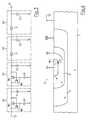
- Figure 4shows in cross-section a possible embodiment of the diodes D, particularly suitable in view of the integration of the charge pump in CMOS integrated devices, such as non-volatile memories.
- a P type substrate 1which represents a common substrate of the chip
- an N type well 2is formed inside the N type well 2
- a P type well 3is formed, and an N+ doped region 4 is formed inside the P type well 3.
- Region 4forms the cathode KA of the diode, while the P type well 3 forms the anode AN.
- the N type well 2is kept biased at VDD (i.e., the more positive voltage inside the chip), while the substrate 1 is conventionally kept grounded. In this way, the P type well 3 is isolated from the P type substrate 1.
- VDDi.e., the more positive voltage inside the chip
Landscapes
- Engineering & Computer Science (AREA)
- Power Engineering (AREA)
- Dc-Dc Converters (AREA)
- Semiconductor Integrated Circuits (AREA)
- Metal-Oxide And Bipolar Metal-Oxide Semiconductor Integrated Circuits (AREA)
- Non-Volatile Memory (AREA)
Description
Claims (5)
- Charge pump comprising a plurality of stages(S1,S2,S3',S4') connected in series between a referencepotential and an output terminal (0) of the charge pump,said plurality of stages comprises afirst group of stages (S1,S2), proximate to said referencepotential, and a second group of stages (S3',S4') proximate tosaid output terminal of the charge pump, each stage of saidfirst group comprising a pass-transistor (M1) with first andsecond terminals respectively connected to an input and anoutput of the stage, and a first capacitor (CL) with a firstplate connected to said output of the stage and a second platedriven by a digital signal (B,D) switching between saidreference voltage and a positive voltage (VDD),characterized in that each stage ofthe second group comprising a junction diode (D) having a firstelectrode connected to an input of the stage and a secondelectrode connected to an output of the stage, and a secondcapacitor (CL') having a first plate connected to said outputof the stage and a second plate driven by a digital signal(B',D') switching between said reference voltage and saidvoltage supply.
- Charge pump according to claim 1,characterized in thateach stage of said first group of stages (S1,S2) furthercomprises a precharge transistor (M2) with a first terminalconnected to the input of the stage, a second terminalconnected to a control electrode of the pass-transistor (M1)and a control terminal connected to the output of the stage,and a second capacitor (CP) with a first plate connected to thecontrol electrode of the pass-transistor, and a second platedriven by a pre-charge digital signal (A,B) switching between the reference voltage and the voltage supply (VDD).
- Charge pump according to claim 2,characterized in thateach of said junction diodes (D) has a first electrode (KA)formed by a doped region (4) of a first conductivity type and asecond electrode (AN) formed by a first well region (3) of asecond conductivity type containing said doped region (4), thefirst well region (3) being in turn formed inside a respectivesecond well region (2) of the first conductivity type formed ina semiconductor substrate of the second conductivity type.
- Charge pump according to claim 3,characterized in thatsaid first conductivity type is the N type and said secondconductivity type is the P type.
- Charge pump according to claim 4,characterized in thatsaid pass-transistor (M1) and said precharge transistor (M2)are P-channel MOSFETs.
Priority Applications (4)
| Application Number | Priority Date | Filing Date | Title |
|---|---|---|---|
| EP96830581AEP0843402B1 (en) | 1996-11-14 | 1996-11-14 | BiCMOS negative charge pump |
| DE69619534TDE69619534T2 (en) | 1996-11-14 | 1996-11-14 | BICMOS negative power charge pump |
| US08/965,068US6016073A (en) | 1996-11-14 | 1997-11-05 | BiCMOS negative charge pump |
| JP9304466AJPH10303311A (en) | 1996-11-14 | 1997-11-06 | Negative electric charge pump |
Applications Claiming Priority (1)
| Application Number | Priority Date | Filing Date | Title |
|---|---|---|---|
| EP96830581AEP0843402B1 (en) | 1996-11-14 | 1996-11-14 | BiCMOS negative charge pump |
Publications (2)
| Publication Number | Publication Date |
|---|---|
| EP0843402A1 EP0843402A1 (en) | 1998-05-20 |
| EP0843402B1true EP0843402B1 (en) | 2002-02-27 |
Family
ID=8226055
Family Applications (1)
| Application Number | Title | Priority Date | Filing Date |
|---|---|---|---|
| EP96830581AExpired - LifetimeEP0843402B1 (en) | 1996-11-14 | 1996-11-14 | BiCMOS negative charge pump |
Country Status (4)
| Country | Link |
|---|---|
| US (1) | US6016073A (en) |
| EP (1) | EP0843402B1 (en) |
| JP (1) | JPH10303311A (en) |
| DE (1) | DE69619534T2 (en) |
Families Citing this family (23)
| Publication number | Priority date | Publication date | Assignee | Title |
|---|---|---|---|---|
| JP3540652B2 (en)* | 1998-04-10 | 2004-07-07 | 三洋電機株式会社 | Charge pump type booster circuit |
| DE69808950T2 (en)* | 1998-12-29 | 2003-12-24 | Stmicroelectronics S.R.L., Agrate Brianza | Integrated circuit producing at least one voltage linear ramp with a low slope |
| JP2001145334A (en)* | 1999-11-15 | 2001-05-25 | Nec Corp | Booster circuit |
| IT1319841B1 (en) | 2000-02-15 | 2003-11-03 | St Microelectronics Srl | HIGH EFFICIENCY BIDIRECTIONAL SURVOLATOR DEVICE. |
| US6268762B1 (en)* | 2000-02-18 | 2001-07-31 | Silicon Storage Technology, Inc. | Output stage for a charge pump and a charge pump made thereby |
| US7053945B1 (en)* | 2000-07-26 | 2006-05-30 | Micron Technolopgy, Inc. | Image sensor having boosted reset |
| US6696883B1 (en)* | 2000-09-20 | 2004-02-24 | Cypress Semiconductor Corp. | Negative bias charge pump |
| US6359814B1 (en)* | 2000-12-29 | 2002-03-19 | Intel Corporation | Negative output voltage charge pump and method therefor |
| JP2006115682A (en)* | 2004-09-14 | 2006-04-27 | Mitsubishi Electric Corp | Voltage generation circuit |
| TW200620795A (en)* | 2004-12-10 | 2006-06-16 | Asour Technology Inc | Voltage-doubling circuit |
| KR100673022B1 (en)* | 2005-12-26 | 2007-01-24 | 삼성전자주식회사 | Charge pump |
| US8115597B1 (en)* | 2007-03-07 | 2012-02-14 | Impinj, Inc. | RFID tags with synchronous power rectifier |
| US8339185B2 (en) | 2010-12-20 | 2012-12-25 | Sandisk 3D Llc | Charge pump system that dynamically selects number of active stages |
| US8981835B2 (en) | 2013-06-18 | 2015-03-17 | Sandisk Technologies Inc. | Efficient voltage doubler |
| US9024680B2 (en) | 2013-06-24 | 2015-05-05 | Sandisk Technologies Inc. | Efficiency for charge pumps with low supply voltages |
| US9077238B2 (en) | 2013-06-25 | 2015-07-07 | SanDisk Technologies, Inc. | Capacitive regulation of charge pumps without refresh operation interruption |
| US9083231B2 (en) | 2013-09-30 | 2015-07-14 | Sandisk Technologies Inc. | Amplitude modulation for pass gate to improve charge pump efficiency |
| US9154027B2 (en) | 2013-12-09 | 2015-10-06 | Sandisk Technologies Inc. | Dynamic load matching charge pump for reduced current consumption |
| US9917507B2 (en) | 2015-05-28 | 2018-03-13 | Sandisk Technologies Llc | Dynamic clock period modulation scheme for variable charge pump load currents |
| US9647536B2 (en) | 2015-07-28 | 2017-05-09 | Sandisk Technologies Llc | High voltage generation using low voltage devices |
| US9520776B1 (en) | 2015-09-18 | 2016-12-13 | Sandisk Technologies Llc | Selective body bias for charge pump transfer switches |
| US10491428B2 (en) | 2018-04-27 | 2019-11-26 | Hewlett Packard Enterprise Development Lp | Current supply for an opto-electronic device |
| US10484089B1 (en)* | 2018-04-27 | 2019-11-19 | Hewlett Packard Enterprise Development Lp | Driver assisted by charge sharing |
Family Cites Families (7)
| Publication number | Priority date | Publication date | Assignee | Title |
|---|---|---|---|---|
| JPS63185054A (en)* | 1987-01-28 | 1988-07-30 | Toshiba Corp | boost circuit |
| KR930008876B1 (en)* | 1990-08-17 | 1993-09-16 | 현대전자산업 주식회사 | High Voltage Generation Circuit of Semiconductor Device |
| US5364801A (en)* | 1990-12-17 | 1994-11-15 | Texas Instruments Incorporated | Method of forming a charge pump circuit |
| KR940005691B1 (en)* | 1991-10-25 | 1994-06-22 | 삼성전자 주식회사 | Charge pumping circuit of the substrate-voltage generating device |
| US5412257A (en)* | 1992-10-20 | 1995-05-02 | United Memories, Inc. | High efficiency N-channel charge pump having a primary pump and a non-cascaded secondary pump |
| TW271011B (en)* | 1994-04-20 | 1996-02-21 | Nippon Steel Corp | |
| EP0772282B1 (en)* | 1995-10-31 | 2000-03-15 | STMicroelectronics S.r.l. | Negative charge pump circuit for electrically erasable semiconductor memory devices |
- 1996
- 1996-11-14EPEP96830581Apatent/EP0843402B1/ennot_activeExpired - Lifetime
- 1996-11-14DEDE69619534Tpatent/DE69619534T2/ennot_activeExpired - Fee Related
- 1997
- 1997-11-05USUS08/965,068patent/US6016073A/ennot_activeExpired - Lifetime
- 1997-11-06JPJP9304466Apatent/JPH10303311A/enactivePending
Also Published As
| Publication number | Publication date |
|---|---|
| DE69619534D1 (en) | 2002-04-04 |
| DE69619534T2 (en) | 2002-10-31 |
| JPH10303311A (en) | 1998-11-13 |
| EP0843402A1 (en) | 1998-05-20 |
| US6016073A (en) | 2000-01-18 |
Similar Documents
| Publication | Publication Date | Title |
|---|---|---|
| EP0843402B1 (en) | BiCMOS negative charge pump | |
| US6130572A (en) | NMOS negative charge pump | |
| EP0836268B1 (en) | Improved positive charge pump | |
| US6603346B2 (en) | Semiconductor booster circuit having cascaded MOS transistors | |
| US5892267A (en) | Multi-stage voltage-boosting circuit with boosted back-gate bias | |
| US4321661A (en) | Apparatus for charging a capacitor | |
| US6359501B2 (en) | Charge-pumping circuits for a low-supply voltage | |
| US6864739B2 (en) | Charge pump stage with body effect minimization | |
| KR101629812B1 (en) | Charge pump circuit comprising multiple gate transistors and method of operating the same | |
| US5347171A (en) | Efficient negative charge pump | |
| US7920018B2 (en) | Booster circuit | |
| US6418040B1 (en) | Bi-directional architecture for a high-voltage cross-coupled charge pump | |
| EP0174694B1 (en) | Circuit for generating a substrate bias | |
| US5412257A (en) | High efficiency N-channel charge pump having a primary pump and a non-cascaded secondary pump | |
| JPH11353888A (en) | Charge pump-type boosting circuit | |
| US6204721B1 (en) | Method and apparatus for switching a well potential in response to an output voltage | |
| US20070069800A1 (en) | Negative charge-pump with circuit to eliminate parasitic diode turn-on | |
| Khouri et al. | Low output resistance charge pump for Flash memory programming | |
| US7148739B2 (en) | Charge pump element with body effect cancellation for early charge pump stages | |
| KR100576812B1 (en) | Charge pump circuit and high voltage generation circuit | |
| US6631081B2 (en) | Capacitive high voltage generator | |
| JP2001245468A (en) | Booster circuit | |
| JP2812269B2 (en) | Boost circuit | |
| JPH0133841B2 (en) | ||
| JPH08125133A (en) | Semiconductor booster circuit |
Legal Events
| Date | Code | Title | Description |
|---|---|---|---|
| PUAI | Public reference made under article 153(3) epc to a published international application that has entered the european phase | Free format text:ORIGINAL CODE: 0009012 | |
| AK | Designated contracting states | Kind code of ref document:A1 Designated state(s):DE FR GB IT | |
| RAP3 | Party data changed (applicant data changed or rights of an application transferred) | Owner name:STMICROELECTRONICS S.R.L. | |
| 17P | Request for examination filed | Effective date:19980914 | |
| AKX | Designation fees paid | Free format text:DE FR GB IT | |
| RBV | Designated contracting states (corrected) | Designated state(s):DE FR GB IT | |
| 17Q | First examination report despatched | Effective date:19990119 | |
| GRAG | Despatch of communication of intention to grant | Free format text:ORIGINAL CODE: EPIDOS AGRA | |
| GRAG | Despatch of communication of intention to grant | Free format text:ORIGINAL CODE: EPIDOS AGRA | |
| GRAH | Despatch of communication of intention to grant a patent | Free format text:ORIGINAL CODE: EPIDOS IGRA | |
| GRAH | Despatch of communication of intention to grant a patent | Free format text:ORIGINAL CODE: EPIDOS IGRA | |
| REG | Reference to a national code | Ref country code:GB Ref legal event code:IF02 | |
| GRAA | (expected) grant | Free format text:ORIGINAL CODE: 0009210 | |
| AK | Designated contracting states | Kind code of ref document:B1 Designated state(s):DE FR GB IT | |
| PG25 | Lapsed in a contracting state [announced via postgrant information from national office to epo] | Ref country code:FR Free format text:LAPSE BECAUSE OF FAILURE TO SUBMIT A TRANSLATION OF THE DESCRIPTION OR TO PAY THE FEE WITHIN THE PRESCRIBED TIME-LIMIT Effective date:20020227 | |
| REF | Corresponds to: | Ref document number:69619534 Country of ref document:DE Date of ref document:20020404 | |
| PG25 | Lapsed in a contracting state [announced via postgrant information from national office to epo] | Ref country code:GB Free format text:LAPSE BECAUSE OF NON-PAYMENT OF DUE FEES Effective date:20021114 | |
| EN | Fr: translation not filed | ||
| PLBE | No opposition filed within time limit | Free format text:ORIGINAL CODE: 0009261 | |
| STAA | Information on the status of an ep patent application or granted ep patent | Free format text:STATUS: NO OPPOSITION FILED WITHIN TIME LIMIT | |
| 26N | No opposition filed | Effective date:20021128 | |
| GBPC | Gb: european patent ceased through non-payment of renewal fee | ||
| PGFP | Annual fee paid to national office [announced via postgrant information from national office to epo] | Ref country code:DE Payment date:20041026 Year of fee payment:9 | |
| PG25 | Lapsed in a contracting state [announced via postgrant information from national office to epo] | Ref country code:IT Free format text:LAPSE BECAUSE OF NON-PAYMENT OF DUE FEES Effective date:20051114 | |
| PG25 | Lapsed in a contracting state [announced via postgrant information from national office to epo] | Ref country code:DE Free format text:LAPSE BECAUSE OF NON-PAYMENT OF DUE FEES Effective date:20060601 |