EP0836268B1 - Improved positive charge pump - Google Patents
Improved positive charge pumpDownload PDFInfo
- Publication number
- EP0836268B1 EP0836268B1EP96830521AEP96830521AEP0836268B1EP 0836268 B1EP0836268 B1EP 0836268B1EP 96830521 AEP96830521 AEP 96830521AEP 96830521 AEP96830521 AEP 96830521AEP 0836268 B1EP0836268 B1EP 0836268B1
- Authority
- EP
- European Patent Office
- Prior art keywords
- charge pump
- voltage
- bulk
- stage
- pump according
- Prior art date
- Legal status (The legal status is an assumption and is not a legal conclusion. Google has not performed a legal analysis and makes no representation as to the accuracy of the status listed.)
- Expired - Lifetime
Links
- 239000003990capacitorSubstances0.000claimsdescription7
- 239000000758substrateSubstances0.000claimsdescription4
- 230000005669field effectEffects0.000claims1
- 239000004065semiconductorSubstances0.000claims1
- 230000000694effectsEffects0.000description7
- 238000010586diagramMethods0.000description4
- 238000004519manufacturing processMethods0.000description2
- 230000010354integrationEffects0.000description1
Images

Classifications
- H—ELECTRICITY
- H02—GENERATION; CONVERSION OR DISTRIBUTION OF ELECTRIC POWER
- H02M—APPARATUS FOR CONVERSION BETWEEN AC AND AC, BETWEEN AC AND DC, OR BETWEEN DC AND DC, AND FOR USE WITH MAINS OR SIMILAR POWER SUPPLY SYSTEMS; CONVERSION OF DC OR AC INPUT POWER INTO SURGE OUTPUT POWER; CONTROL OR REGULATION THEREOF
- H02M3/00—Conversion of DC power input into DC power output
- H02M3/02—Conversion of DC power input into DC power output without intermediate conversion into AC
- H02M3/04—Conversion of DC power input into DC power output without intermediate conversion into AC by static converters
- H02M3/06—Conversion of DC power input into DC power output without intermediate conversion into AC by static converters using resistors or capacitors, e.g. potential divider
- H02M3/07—Conversion of DC power input into DC power output without intermediate conversion into AC by static converters using resistors or capacitors, e.g. potential divider using capacitors charged and discharged alternately by semiconductor devices with control electrode, e.g. charge pumps
- H02M3/073—Charge pumps of the Schenkel-type
Definitions
- the present inventionrelates to an improved positive charge pump, particularly for the integration in CMOS integrated circuits such as non-volatile memory devices.
- a positive charge pumpis a circuit suitable for generating, starting from a positive voltage having a predetermined value, a higher voltage.
- a positive charge pumpcomprises a plurality of stages connected in series between an input terminal of the charge pump connected to a positive voltage supply and an output terminal of the charge pump.
- each stagesubstantially comprises a diode-connected N-channel MOSFET and a capacitor having one plate connected to the source electrode of the MOSFET and another plate driven by a respective digital signal periodically varying between ground and the voltage supply.
- the voltage gain of each stageis equal to the value of the voltage supply minus the threshold voltage of the N-channel MOSFET.
- More sophisticated charge pumpshave stages wherein the diode-connected MOSFET is replaced by a pass-transistor, and comprise circuits for boosting the gate voltage of the pass transistor. In this way, as long as the body effect on the threshold voltage of the pass-transistors is not very high, it is possbile to partially compensate the increase in the threshold voltage.
- the main problem of these circuitsresides in the fact that, due to the body effect, the threshold voltage of the N-channel MOSFETs becomes higher and higher moving from the stages proximate to the input terminal to the stages proximate to the output terminal of the charge pump. This causes a reduction in the voltage gain of the stages, and makes it necessary to increase the number of stages in order to generate a given output voltage.
- a greater number of stagesmeans a greater occupation of area in the chip, and a higher power consumption. Furthermore, it is not possible to generate output voltages higher than a given value, because when the threshold voltage (with body effect) of the N-channel MOSFETs becomes higher than the voltage supply, the addition of further stages is completely unuseful. Even the more sophisticated solution becomes less and less effective moving from the input terminal to the output terminal of the charge pump, and the final stages have a poor efficiency.
- Document EP303193describes a charge pump according to the preamble of claim 1.
- a charge pumpcomprising a plurality of stages connected in series, an input terminal of the charge pump being connected to a voltage supply and an output terminal of the charge pump providing an output voltage higher than the voltage supply, each stage comprising unidirectional current flow MOS transistor means connected between a stage input terminal and a stage output terminal allowing current to flow only from said stage input terminal to said stage output terminal, and a first capacitor with one plate connected to said stage output terminal and another plate driven by a respective first digital signal periodically switched between ground and said voltage supply, characterized in that the unidirectional current flow MOS transistor means of the stages have independent bulk electrodes, and in that said charge pump comprises also a bias voltage generator circuit provided for biasing the bulk electrodes of said unidirectional current flow MOS transistor means at respective bulk potentials which become progressively higher going from the stages proximate to said input terminal to the stages proximate to said output terminal of the charge pump.
- the present inventionit is possible to completely eliminate the influence of the body effect on the threshold voltage of the unidirectional current flow MOS transistor means.
- the efficiency of the stages of the charge pump in terms of voltage gainremains substantially constant in going from the input terminal to the output terminal of the charge pump. It is thus possible to generate a given output voltage with a smaller number of stages, with a great reduction in chip area and power consumption.
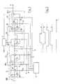
- FIG. 1there is illustrated a positive charge pump according to one embodiment of the present invention.
- the charge pumpcomprises a plurality (four in this example) of stages S1-S4, connected in series between an input terminal I of the charge pump connected to a voltage supply VDD and an output terminal 0 of the charge pump.
- VDDis the voltage supply of the device.
- Each stagecomprises a pass-transistor M1 formed by an N-channel MOSFET, connected between a stage input terminal SI and a stage output terminal SO; a capacitor C1 having one plate connected to the stage output terminal SO and another plate driven by a respective phase signal B or D, depending on the particular stage; a precharge transistor M2 formed by an N-channel MOSFET with an electrode connected to the stage input terminal SI, another electrode connected to the gate electrode of M1 and a gate electrode connected to the stage output terminal SO; and a boosting capacitor C2 having one plate connected to the gate electrode of M1 and another plate driven by a respective phase signal A or C, depending on the particular stage.
- Signals A, B, C and Dare generated by a timing signal generator 1.
- signals A, B, C and Dare depicted in Fig. 2. These signals are digital signals periodically switching between ground and the voltage supply; signals A and D are substantially in phase to each other, and the same holds true for signals B and C; signals A and D are respectively in phase opposition to signals B and C.
- MOSFETs M1 and M2 in each stagehave bulk electrodes which are independent from the bulk electrodes of MOSFETs M1 and M2 in the other stages.
- the last stage S4 of the charge pumpfurther comprises an N-channel MOSFET M13 with source connected to the stage input terminal SI, drain connected to the output terminal 0 of the charge pump, gate connected to the gate of M1 and bulk connected to the bulk of M1.
- the charge pumpfurther comprises a bias voltage generator 2 which generates three bias voltages B01, B2, B3.
- Bias voltage B01is used to bias the bulk electrodes of MOSFETs M1 and M2 in the first and second stages S1 and S2; bias voltages B2 and B3 are used to bias the bulk electrodes of MOSFETs M1 and M2 in the third and fourth stages S3 and S4, respectively.
- the bias voltage generator 2is supplied with the output voltage O of the charge pump; the bias voltage generator 2 is also supplied with an enable signal EN.
- the bias voltage of the bulk electrode of MOSFETs M1 and M2should be sufficiently high to limit the body effect; second, the voltage of the bulk electrode of the MOSFETs must always be Lower or at most equal to the voltage of the source electrodes of the MOSFETs, to prevent forward biasing of the source/bulk junction.
- FIG. 3is a circuit diagram of a preferred embodiment of the bias voltage generator 2 suitable to satisfy the above-mentioned requirements.
- the circuitcomprises a voltage divider 3 formed by four diode-connected P-channel MOSFETs M3, M4, M5 and M6 connected in series between the output voltage 0 of the charge pump and ground.
- Bias voltage B3is derived from a node N1 of the voltage divider between MOSFETs M3 and M4, with the interposition of a diode-connected P-channel MOSFET M7.
- bias voltage B2is derived from a node N2 of the voltage divider between M4 and M5, with the interposition of a diode-connected P-channel MOSFET M8, and bias voltage B01 is derived from a node N3 of the voltage divider between M5 and M6, with the interposition of a diode-connected P-channel MOSFET M9.
- the output voltage V(O) of the charge pumpis divided for the number of stages of the charge pump.
- the circuit of Figure 3ensures that the bias voltages V(B01), V(B2) and V(B3) are respectively equal to the lower among the voltages of the source and drain electrodes of MOSFETs M1 and M2 in stages S1, S2, S3 and S4 (as known, in a charge pump the source and drain electrodes of the MOSFETs are not univocally defined); thanks to this, the body effect on the threshold voltage of said MOSFETs is eliminated, and at the same time it is assured that the source/bulk junctions of the MOSFETs are not forward biased.
- MOSFETs M7, M8 and M9introduce a safety margin sufficient to prevent that, due to possible spurious variations, the bias voltages V(B01), V(B2) and V(B3) directly bias the source/bulk junctions of the MOSFETs of the charge pump.
- the MOSFETs of the charge pumphave independent bulk electrodes and thanks to the provision of the bias voltage generator 2 which biases the bulk electrodes of said MOSFETs, it is possible to minimize the number of stage of the charge pump required for generating a given output voltage; this means a reduction in the chip area and in the power consumption. Furthermore, it is possible to generate output voltages of any value, by simply adding stages to the charge pump: each stage will have a voltage gain which is not affected by the body effect. Biasing the bulk electrodes of the MOSFETs also increase the reliability of the device, in fact when the MOSFETs are in the off condition the voltage applied to their gate oxide is lower.
- FIG 4shows in cross-section, side by side, a suitable structure of the N-channel MOSFETs M1 and M2 of the charge pump of Figure 1 and the structure of the P-channel MOSFETs M3-M9 of the bias voltage generator 2 of Figure 3.
- Each one of MOSFETs M1 and M2is formed inside a respective P type well 4, formed in turn inside an N type well 5 provided in a P type substrate 6.
- N type well 5provided in a P type substrate 6.
- an insulated gate (gate electrode G of the MOSFET)is conventionally provided between regions 7 and 8; further, a P+ well contact region 9 is formed; a similar N+ well contact region 10 is formed inside the N type well 5.
- the P type well 4 and the P+ contact region 9form the bulk electrode BUN of the MOSFET, and are short-circuited to the N+ contact region 10 to the N type well 5.
- a so-called "triple well” manufacturing processis required; in fact, in order to have independent bulk electrodes which can be biased at different potentials, it is necessary that the bulk electrodes are electrically isolated from one another; this can be achieved by forming the N-channel MOSFETs inside separate P type wells 4 formed in turn inside separate N type wells 5; in a single or double well manufacturing process, the N-channel MOSFETs would be formed directly inside the P type substrate (which is normally kept grounded), and they would have a common bulk electrode.
- Each one of the P-channel MOSFETs M3-M9is instead formed inside a respective N type well 11; the bulk electrode BUP of such a MOSFET is formed by the N type well and by an N+ contact region 12 formed inside the N type well 11.
- each stagecomprises only a diode-connected N-channel MOSFET and a capacitor.
Landscapes
- Engineering & Computer Science (AREA)
- Power Engineering (AREA)
- Dc-Dc Converters (AREA)
Description
Claims (11)
- Charge pump comprising a plurality of stages (S1-S4)connected in series, an input terminal (I) of the charge pumpbeing connected to a voltage supply (VDD) and an outputterminal (O) of the charge pump providing an output voltagehigher than the voltage supply, each stage comprisingunidirectional current flow MOS transistor means (M1) connectedbetween a stage input terminal (SI) and a stage output terminal(SO) allowing current to flow only from said stage inputterminal to said stage output terminal, and a first capacitor(C1) with one plate connected to said stage output terminal andanother plate driven by a respective first digital signal (B,D)periodically switched between ground and said voltage supply,characterized in that the unidirectional current flow MOStransistor means (M1) of the stages have independent bulkelectrodes (BUN), andin that said charge pump comprises also a bias voltage generator circuit(2) provided for biasing the bulk electrodes of saidunidirectional current flow MOS transistor means at respectivebulk potentials (B01,B2,B3) which become progressively highergoing from the stages proximate to said input terminal to thestages proximate to said output terminal of the charge pump.
- Charge pump according to claim 1,characterized in thatsaid bulk potentials (B01,B2,B3) can be Lower or higher thansaid voltage supply (VDD).
- Charge pump according to claim 2,characterized in thateach of said bulk potentials (B01,B2,B3) is at most equal tothe minimum between a source voltage and a drain voltage of therespective unidirectional current flow MOS transistor means(M1).
- Charge pump according to claim 3,characterized in that said bias voltage generator circuit (2) generates said bulkpotentials (B01,B2,B3) starting from the output voltage of thecharge pump, and contains voltage dividing means (3).
- Charge pump according to claim 4,characterized in thatsaid voltage dividing means (3) comprise a voltage dividerinserted between the output terminal of the charge pump andground and having a number of intermediate nodes substantiallyequal to the number of stages of the charge pump.
- Charge pump according to claim 5,characterized in thateach of said bulk potentials (B01,B2,B3) is at most equal tothe voltage of a respective intermediate node of the voltagepartitioner (3).
- Charge pump according to claim 6,characterized in thateach of said bulk potentials (B01,B2,B3) is equal to thevoltage of the respective intermediate node of the voltagepartitioner (3), minus a prescribed voltage margin.
- Charge pump according to claim 7,characterized in thateach of said unidirectional current flow MOS transistor meanscomprises a diode-connected N-channel MOSFET.
- Charge pump according to claim 7,characterized in thateach of said unidirectional current flow MOS transistor means(M1) comprises an N-channel MOS field effect pass transistor,each stage further comprising gate voltage boosting means(M2,C2) for boosting a gate voltage of the pass transistor.
- Charge pump according to claim 9,characterized in thatsaid gate voltage boosting means (M2,C2) comprise an N-channelpre-charge MOSFET (M2) with first and second electrodesrespectively connected to the stage input terminal (SI) and tothe gate electrode of the pass MOSFET (M1) and a gate electrodeconnected to the stage output terminal (SO), and a second capacitor (C2) with one plate connected to the gate electrodeof the pass MOSFET and another plate driven by a respectivesecond digital signal (A,C) periodically switching betweenground and the voltage supply and substantially in phaseopposition with respect to the first digital signal (B,D).
- Charge pump according to claim 1,characterized in thateach of said unidirectional current flow MOS transistor means(M1) comprises a first well region (5) of a first conductivitytype formed in a semiconductor substrate (6) of a secondconductivity type, a second well region (4) of the secondconductivity type formed inside the first well region, sourceand drain regions (7,8) of the first conductivity type formedinside the second well region (4) and an insulated gatedisposed above the second well region between the source anddrain regions, the second well region (4) forming the bulkelectrode of the MOS transistor means being isolated from thesubstrate (6) by the first well region (5).
Priority Applications (3)
| Application Number | Priority Date | Filing Date | Title |
|---|---|---|---|
| EP96830521AEP0836268B1 (en) | 1996-10-11 | 1996-10-11 | Improved positive charge pump |
| DE69619112TDE69619112D1 (en) | 1996-10-11 | 1996-10-11 | Improved positive charge pump |
| US08/946,727US6075402A (en) | 1996-10-11 | 1997-10-08 | Positive charge pump |
Applications Claiming Priority (1)
| Application Number | Priority Date | Filing Date | Title |
|---|---|---|---|
| EP96830521AEP0836268B1 (en) | 1996-10-11 | 1996-10-11 | Improved positive charge pump |
Publications (2)
| Publication Number | Publication Date |
|---|---|
| EP0836268A1 EP0836268A1 (en) | 1998-04-15 |
| EP0836268B1true EP0836268B1 (en) | 2002-02-06 |
Family
ID=8226029
Family Applications (1)
| Application Number | Title | Priority Date | Filing Date |
|---|---|---|---|
| EP96830521AExpired - LifetimeEP0836268B1 (en) | 1996-10-11 | 1996-10-11 | Improved positive charge pump |
Country Status (3)
| Country | Link |
|---|---|
| US (1) | US6075402A (en) |
| EP (1) | EP0836268B1 (en) |
| DE (1) | DE69619112D1 (en) |
Cited By (3)
| Publication number | Priority date | Publication date | Assignee | Title |
|---|---|---|---|---|
| CN101373927B (en)* | 2007-08-20 | 2010-12-01 | 台湾积体电路制造股份有限公司 | Charge pump circuit, method of operating the same, and semiconductor device |
| CN103872903A (en)* | 2014-03-11 | 2014-06-18 | 中山芯达电子科技有限公司 | Stackable voltage generator |
| US9379103B2 (en) | 2012-10-17 | 2016-06-28 | Semtech Corporation | Semiconductor device and method of preventing latch-up in a charge pump circuit |
Families Citing this family (58)
| Publication number | Priority date | Publication date | Assignee | Title |
|---|---|---|---|---|
| US6768165B1 (en) | 1997-08-01 | 2004-07-27 | Saifun Semiconductors Ltd. | Two bit non-volatile electrically erasable and programmable semiconductor memory cell utilizing asymmetrical charge trapping |
| US6353356B1 (en)* | 1999-08-30 | 2002-03-05 | Micron Technology, Inc. | High voltage charge pump circuits |
| JP2001145335A (en)* | 1999-11-11 | 2001-05-25 | Nec Corp | Booster circuit |
| US6191963B1 (en)* | 2000-01-19 | 2001-02-20 | Lucent Technologies Inc. | Charge pump with no diode drop at output stage |
| IT1319841B1 (en) | 2000-02-15 | 2003-11-03 | St Microelectronics Srl | HIGH EFFICIENCY BIDIRECTIONAL SURVOLATOR DEVICE. |
| JP3614747B2 (en)* | 2000-03-07 | 2005-01-26 | Necエレクトロニクス株式会社 | BOOST CIRCUIT, IC CARD WITH THE SAME AND ELECTRONIC DEVICE WITH THE SAME |
| US6801076B1 (en)* | 2000-04-28 | 2004-10-05 | Micron Technology, Inc. | High output high efficiency low voltage charge pump |
| US6833752B2 (en) | 2000-04-28 | 2004-12-21 | Micron Technology, Inc. | High output high efficiency low voltage charge pump |
| US6359500B1 (en)* | 2000-12-11 | 2002-03-19 | Stmicroelectronics S.R.L. | Charge pump with efficient switching techniques |
| DE10064819A1 (en)* | 2000-12-22 | 2002-07-18 | Koninkl Philips Electronics Nv | Adaptive phase control for charge pumps |
| US6584017B2 (en) | 2001-04-05 | 2003-06-24 | Saifun Semiconductors Ltd. | Method for programming a reference cell |
| US6577514B2 (en) | 2001-04-05 | 2003-06-10 | Saifun Semiconductors Ltd. | Charge pump with constant boosted output voltage |
| US6677805B2 (en)* | 2001-04-05 | 2004-01-13 | Saifun Semiconductors Ltd. | Charge pump stage with body effect minimization |
| DE10137698A1 (en)* | 2001-08-01 | 2003-02-27 | Infineon Technologies Ag | Method and integrated circuit for increasing a voltage |
| US6646493B2 (en) | 2001-08-14 | 2003-11-11 | Micron Technology, Inc. | Voltage charge pump with circuit to prevent pass device latch-up |
| US6577552B2 (en) | 2001-08-30 | 2003-06-10 | Micron Technology, Inc. | Apparatus and method for generating an oscillating signal |
| US6791396B2 (en)* | 2001-10-24 | 2004-09-14 | Saifun Semiconductors Ltd. | Stack element circuit |
| US6700818B2 (en) | 2002-01-31 | 2004-03-02 | Saifun Semiconductors Ltd. | Method for operating a memory device |
| US6917544B2 (en) | 2002-07-10 | 2005-07-12 | Saifun Semiconductors Ltd. | Multiple use memory chip |
| US7136304B2 (en) | 2002-10-29 | 2006-11-14 | Saifun Semiconductor Ltd | Method, system and circuit for programming a non-volatile memory array |
| US6842383B2 (en) | 2003-01-30 | 2005-01-11 | Saifun Semiconductors Ltd. | Method and circuit for operating a memory cell using a single charge pump |
| US20040151032A1 (en)* | 2003-01-30 | 2004-08-05 | Yan Polansky | High speed and low noise output buffer |
| US7178004B2 (en) | 2003-01-31 | 2007-02-13 | Yan Polansky | Memory array programming circuit and a method for using the circuit |
| US6885244B2 (en) | 2003-03-24 | 2005-04-26 | Saifun Semiconductors Ltd. | Operational amplifier with fast rise time |
| US7142464B2 (en) | 2003-04-29 | 2006-11-28 | Saifun Semiconductors Ltd. | Apparatus and methods for multi-level sensing in a memory array |
| US6906966B2 (en) | 2003-06-16 | 2005-06-14 | Saifun Semiconductors Ltd. | Fast discharge for program and verification |
| US7123532B2 (en) | 2003-09-16 | 2006-10-17 | Saifun Semiconductors Ltd. | Operating array cells with matched reference cells |
| US7050319B2 (en)* | 2003-12-03 | 2006-05-23 | Micron Technology, Inc. | Memory architecture and method of manufacture and operation thereof |
| US7176728B2 (en)* | 2004-02-10 | 2007-02-13 | Saifun Semiconductors Ltd | High voltage low power driver |
| US8339102B2 (en)* | 2004-02-10 | 2012-12-25 | Spansion Israel Ltd | System and method for regulating loading on an integrated circuit power supply |
| WO2005094178A2 (en) | 2004-04-01 | 2005-10-13 | Saifun Semiconductors Ltd. | Method, circuit and systems for erasing one or more non-volatile memory cells |
| US7190212B2 (en)* | 2004-06-08 | 2007-03-13 | Saifun Semiconductors Ltd | Power-up and BGREF circuitry |
| US7256438B2 (en)* | 2004-06-08 | 2007-08-14 | Saifun Semiconductors Ltd | MOS capacitor with reduced parasitic capacitance |
| US7187595B2 (en)* | 2004-06-08 | 2007-03-06 | Saifun Semiconductors Ltd. | Replenishment for internal voltage |
| US7317633B2 (en) | 2004-07-06 | 2008-01-08 | Saifun Semiconductors Ltd | Protection of NROM devices from charge damage |
| US7095655B2 (en) | 2004-08-12 | 2006-08-22 | Saifun Semiconductors Ltd. | Dynamic matching of signal path and reference path for sensing |
| US7638850B2 (en) | 2004-10-14 | 2009-12-29 | Saifun Semiconductors Ltd. | Non-volatile memory structure and method of fabrication |
| US7248096B2 (en) | 2004-11-22 | 2007-07-24 | Stmicroelectronics S.R.L. | Charge pump circuit with dynamic biasing of pass transistors |
| EP1686592A3 (en) | 2005-01-19 | 2007-04-25 | Saifun Semiconductors Ltd. | Partial erase verify |
| US7561866B2 (en)* | 2005-02-22 | 2009-07-14 | Impinj, Inc. | RFID tags with power rectifiers that have bias |
| US8053812B2 (en) | 2005-03-17 | 2011-11-08 | Spansion Israel Ltd | Contact in planar NROM technology |
| US8400841B2 (en) | 2005-06-15 | 2013-03-19 | Spansion Israel Ltd. | Device to program adjacent storage cells of different NROM cells |
| US7184313B2 (en) | 2005-06-17 | 2007-02-27 | Saifun Semiconductors Ltd. | Method circuit and system for compensating for temperature induced margin loss in non-volatile memory cells |
| US7786512B2 (en) | 2005-07-18 | 2010-08-31 | Saifun Semiconductors Ltd. | Dense non-volatile memory array and method of fabrication |
| US7668017B2 (en) | 2005-08-17 | 2010-02-23 | Saifun Semiconductors Ltd. | Method of erasing non-volatile memory cells |
| US7221138B2 (en) | 2005-09-27 | 2007-05-22 | Saifun Semiconductors Ltd | Method and apparatus for measuring charge pump output current |
| US7352627B2 (en) | 2006-01-03 | 2008-04-01 | Saifon Semiconductors Ltd. | Method, system, and circuit for operating a non-volatile memory array |
| US7808818B2 (en) | 2006-01-12 | 2010-10-05 | Saifun Semiconductors Ltd. | Secondary injection for NROM |
| US7692961B2 (en) | 2006-02-21 | 2010-04-06 | Saifun Semiconductors Ltd. | Method, circuit and device for disturb-control of programming nonvolatile memory cells by hot-hole injection (HHI) and by channel hot-electron (CHE) injection |
| US8253452B2 (en) | 2006-02-21 | 2012-08-28 | Spansion Israel Ltd | Circuit and method for powering up an integrated circuit and an integrated circuit utilizing same |
| US7760554B2 (en) | 2006-02-21 | 2010-07-20 | Saifun Semiconductors Ltd. | NROM non-volatile memory and mode of operation |
| US7638835B2 (en) | 2006-02-28 | 2009-12-29 | Saifun Semiconductors Ltd. | Double density NROM with nitride strips (DDNS) |
| US7701779B2 (en) | 2006-04-27 | 2010-04-20 | Sajfun Semiconductors Ltd. | Method for programming a reference cell |
| US7605579B2 (en) | 2006-09-18 | 2009-10-20 | Saifun Semiconductors Ltd. | Measuring and controlling current consumption and output current of charge pumps |
| US9343961B1 (en)* | 2013-09-13 | 2016-05-17 | Qualtre, Inc. | Ultrahigh voltage charge pump apparatus implemented with low voltage technology |
| US10713549B1 (en)* | 2017-05-23 | 2020-07-14 | Impinj, Inc. | RFID tag rectifiers with bias current reuse |
| US11188803B1 (en) | 2019-03-07 | 2021-11-30 | Impinj, Inc. | Rectifier backflow reduction via biasing |
| CN113872435A (en)* | 2021-10-19 | 2021-12-31 | 普冉半导体(上海)股份有限公司 | Single-stage circuit of positive and negative voltage charge pump and four-phase charge pump circuit |
Family Cites Families (7)
| Publication number | Priority date | Publication date | Assignee | Title |
|---|---|---|---|---|
| JPS6445157A (en)* | 1987-08-13 | 1989-02-17 | Toshiba Corp | Semiconductor integrated circuit |
| IT1221261B (en)* | 1988-06-28 | 1990-06-27 | Sgs Thomson Microelectronics | OMOS VOLTAGE MULTIPLIER |
| IT1246238B (en)* | 1990-02-16 | 1994-11-17 | Sgs Thomson Microelectronics | SWITCHED PHASE OSCILLATOR FOR PILOTING A VOLTAGE MULTIPLIER |
| CA2034400A1 (en)* | 1990-04-30 | 1991-10-31 | James Vincent Crivello | Method for making triarylsulfonium hexafluorometal or metalloid salts |
| US5081371A (en)* | 1990-11-07 | 1992-01-14 | U.S. Philips Corp. | Integrated charge pump circuit with back bias voltage reduction |
| FR2696598B1 (en)* | 1992-10-01 | 1994-11-04 | Sgs Thomson Microelectronics | Charge pump type voltage booster circuit with bootstrap oscillator. |
| JP3307453B2 (en)* | 1993-03-18 | 2002-07-24 | ソニー株式会社 | Boost circuit |
- 1996
- 1996-10-11EPEP96830521Apatent/EP0836268B1/ennot_activeExpired - Lifetime
- 1996-10-11DEDE69619112Tpatent/DE69619112D1/ennot_activeExpired - Lifetime
- 1997
- 1997-10-08USUS08/946,727patent/US6075402A/ennot_activeExpired - Lifetime
Cited By (4)
| Publication number | Priority date | Publication date | Assignee | Title |
|---|---|---|---|---|
| CN101373927B (en)* | 2007-08-20 | 2010-12-01 | 台湾积体电路制造股份有限公司 | Charge pump circuit, method of operating the same, and semiconductor device |
| US9379103B2 (en) | 2012-10-17 | 2016-06-28 | Semtech Corporation | Semiconductor device and method of preventing latch-up in a charge pump circuit |
| CN103872903A (en)* | 2014-03-11 | 2014-06-18 | 中山芯达电子科技有限公司 | Stackable voltage generator |
| CN103872903B (en)* | 2014-03-11 | 2016-08-17 | 中山芯达电子科技有限公司 | Stack voltage generator |
Also Published As
| Publication number | Publication date |
|---|---|
| US6075402A (en) | 2000-06-13 |
| EP0836268A1 (en) | 1998-04-15 |
| DE69619112D1 (en) | 2002-03-21 |
Similar Documents
| Publication | Publication Date | Title |
|---|---|---|
| EP0836268B1 (en) | Improved positive charge pump | |
| US6130572A (en) | NMOS negative charge pump | |
| JP2718375B2 (en) | Charge pump circuit | |
| US6819162B2 (en) | Charge pump for negative voltages | |
| US4922402A (en) | CMOS voltage multiplier | |
| EP0485016B1 (en) | Integrated charge pump circuit with back bias voltage reduction | |
| US6603346B2 (en) | Semiconductor booster circuit having cascaded MOS transistors | |
| US7466189B2 (en) | Semiconductor integrated circuit | |
| EP0843402B1 (en) | BiCMOS negative charge pump | |
| US7602231B2 (en) | Charge-pump circuit | |
| US20080042731A1 (en) | High efficiency bi-directional charge pump circuit | |
| US7589583B2 (en) | Charge pump circuit | |
| US6418040B1 (en) | Bi-directional architecture for a high-voltage cross-coupled charge pump | |
| JP4790945B2 (en) | Charge pump circuit | |
| US7002399B2 (en) | Basic stage for a charge pump circuit | |
| US7239193B2 (en) | Semiconductor device | |
| US20060273843A1 (en) | High efficiency bi-directional charge pump circuit | |
| JP3154727B2 (en) | Equipment for voltage multiplication | |
| JPH11308856A (en) | Charge pump circuit device | |
| JPH07298607A (en) | Semiconductor booster circuit | |
| JPH0246162A (en) | CMOS voltage amplifier | |
| JP3569354B2 (en) | Semiconductor booster circuit | |
| US6316986B1 (en) | Method and device for voltage multiplication | |
| JP2901608B2 (en) | Ring oscillation circuit | |
| JP2005045934A (en) | Charge pump circuit |
Legal Events
| Date | Code | Title | Description |
|---|---|---|---|
| PUAI | Public reference made under article 153(3) epc to a published international application that has entered the european phase | Free format text:ORIGINAL CODE: 0009012 | |
| AK | Designated contracting states | Kind code of ref document:A1 Designated state(s):DE FR GB IT | |
| AX | Request for extension of the european patent | Free format text:AL;LT;LV;SI | |
| RAP3 | Party data changed (applicant data changed or rights of an application transferred) | Owner name:STMICROELECTRONICS S.R.L. | |
| 17P | Request for examination filed | Effective date:19980721 | |
| AKX | Designation fees paid | Free format text:DE FR GB IT | |
| RBV | Designated contracting states (corrected) | Designated state(s):DE FR GB IT | |
| GRAG | Despatch of communication of intention to grant | Free format text:ORIGINAL CODE: EPIDOS AGRA | |
| 17Q | First examination report despatched | Effective date:20010328 | |
| GRAG | Despatch of communication of intention to grant | Free format text:ORIGINAL CODE: EPIDOS AGRA | |
| GRAH | Despatch of communication of intention to grant a patent | Free format text:ORIGINAL CODE: EPIDOS IGRA | |
| GRAH | Despatch of communication of intention to grant a patent | Free format text:ORIGINAL CODE: EPIDOS IGRA | |
| GRAA | (expected) grant | Free format text:ORIGINAL CODE: 0009210 | |
| REG | Reference to a national code | Ref country code:GB Ref legal event code:IF02 | |
| AK | Designated contracting states | Kind code of ref document:B1 Designated state(s):DE FR GB IT | |
| PG25 | Lapsed in a contracting state [announced via postgrant information from national office to epo] | Ref country code:FR Free format text:LAPSE BECAUSE OF FAILURE TO SUBMIT A TRANSLATION OF THE DESCRIPTION OR TO PAY THE FEE WITHIN THE PRESCRIBED TIME-LIMIT Effective date:20020206 | |
| REF | Corresponds to: | Ref document number:69619112 Country of ref document:DE Date of ref document:20020321 | |
| PG25 | Lapsed in a contracting state [announced via postgrant information from national office to epo] | Ref country code:DE Free format text:LAPSE BECAUSE OF FAILURE TO SUBMIT A TRANSLATION OF THE DESCRIPTION OR TO PAY THE FEE WITHIN THE PRESCRIBED TIME-LIMIT Effective date:20020507 | |
| PG25 | Lapsed in a contracting state [announced via postgrant information from national office to epo] | Ref country code:GB Free format text:LAPSE BECAUSE OF NON-PAYMENT OF DUE FEES Effective date:20021011 | |
| EN | Fr: translation not filed | ||
| PLBE | No opposition filed within time limit | Free format text:ORIGINAL CODE: 0009261 | |
| STAA | Information on the status of an ep patent application or granted ep patent | Free format text:STATUS: NO OPPOSITION FILED WITHIN TIME LIMIT | |
| 26N | No opposition filed | Effective date:20021107 | |
| GBPC | Gb: european patent ceased through non-payment of renewal fee | Effective date:20021011 | |
| PG25 | Lapsed in a contracting state [announced via postgrant information from national office to epo] | Ref country code:IT Free format text:LAPSE BECAUSE OF NON-PAYMENT OF DUE FEES;WARNING: LAPSES OF ITALIAN PATENTS WITH EFFECTIVE DATE BEFORE 2007 MAY HAVE OCCURRED AT ANY TIME BEFORE 2007. THE CORRECT EFFECTIVE DATE MAY BE DIFFERENT FROM THE ONE RECORDED. Effective date:20051011 |