EP0836194B1 - Semiconductor device - Google Patents
Semiconductor deviceDownload PDFInfo
- Publication number
- EP0836194B1 EP0836194B1EP97203535AEP97203535AEP0836194B1EP 0836194 B1EP0836194 B1EP 0836194B1EP 97203535 AEP97203535 AEP 97203535AEP 97203535 AEP97203535 AEP 97203535AEP 0836194 B1EP0836194 B1EP 0836194B1
- Authority
- EP
- European Patent Office
- Prior art keywords
- back bias
- bias voltage
- semiconductor device
- substrate
- voltage
- Prior art date
- Legal status (The legal status is an assumption and is not a legal conclusion. Google has not performed a legal analysis and makes no representation as to the accuracy of the status listed.)
- Expired - Lifetime
Links
Images


Classifications
- H—ELECTRICITY
- H03—ELECTRONIC CIRCUITRY
- H03K—PULSE TECHNIQUE
- H03K19/00—Logic circuits, i.e. having at least two inputs acting on one output; Inverting circuits
- H03K19/0008—Arrangements for reducing power consumption
- H03K19/0016—Arrangements for reducing power consumption by using a control or a clock signal, e.g. in order to apply power supply
- G—PHYSICS
- G11—INFORMATION STORAGE
- G11C—STATIC STORES
- G11C11/00—Digital stores characterised by the use of particular electric or magnetic storage elements; Storage elements therefor
- G11C11/21—Digital stores characterised by the use of particular electric or magnetic storage elements; Storage elements therefor using electric elements
- G11C11/34—Digital stores characterised by the use of particular electric or magnetic storage elements; Storage elements therefor using electric elements using semiconductor devices
- G11C11/40—Digital stores characterised by the use of particular electric or magnetic storage elements; Storage elements therefor using electric elements using semiconductor devices using transistors
- G11C11/401—Digital stores characterised by the use of particular electric or magnetic storage elements; Storage elements therefor using electric elements using semiconductor devices using transistors forming cells needing refreshing or charge regeneration, i.e. dynamic cells
- G11C11/4063—Auxiliary circuits, e.g. for addressing, decoding, driving, writing, sensing or timing
- G11C11/407—Auxiliary circuits, e.g. for addressing, decoding, driving, writing, sensing or timing for memory cells of the field-effect type
- G11C11/4074—Power supply or voltage generation circuits, e.g. bias voltage generators, substrate voltage generators, back-up power, power control circuits
- G—PHYSICS
- G11—INFORMATION STORAGE
- G11C—STATIC STORES
- G11C5/00—Details of stores covered by group G11C11/00
- G11C5/14—Power supply arrangements, e.g. power down, chip selection or deselection, layout of wirings or power grids, or multiple supply levels
- G11C5/145—Applications of charge pumps; Boosted voltage circuits; Clamp circuits therefor
- G11C5/146—Substrate bias generators
- H—ELECTRICITY
- H10—SEMICONDUCTOR DEVICES; ELECTRIC SOLID-STATE DEVICES NOT OTHERWISE PROVIDED FOR
- H10D—INORGANIC ELECTRIC SEMICONDUCTOR DEVICES
- H10D84/00—Integrated devices formed in or on semiconductor substrates that comprise only semiconducting layers, e.g. on Si wafers or on GaAs-on-Si wafers
- H10D84/80—Integrated devices formed in or on semiconductor substrates that comprise only semiconducting layers, e.g. on Si wafers or on GaAs-on-Si wafers characterised by the integration of at least one component covered by groups H10D12/00 or H10D30/00, e.g. integration of IGFETs
- H—ELECTRICITY
- H10—SEMICONDUCTOR DEVICES; ELECTRIC SOLID-STATE DEVICES NOT OTHERWISE PROVIDED FOR
- H10D—INORGANIC ELECTRIC SEMICONDUCTOR DEVICES
- H10D89/00—Aspects of integrated devices not covered by groups H10D84/00 - H10D88/00
- H10D89/211—Design considerations for internal polarisation
- H10D89/213—Design considerations for internal polarisation in field-effect devices
Definitions
- the present inventionrelates to a semiconductor device including a MOS (Metal Oxide Semiconductor) field effect transistor (hereinafter referred to as "MOSFET”) formed on a semiconductor substrate and, more particularly, to an improvement in supplying a substrate bias voltage.
- MOSMetal Oxide Semiconductor field effect transistor
- a semiconductor devicesuch as a dynamic random access memory and a static random access memory is constituted by a number of MOS transistors formed on one semiconductor substrate. Normally, the potential of the semiconductor substrate is constantly maintained in a predetermined range in such a semiconductor device.
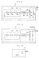
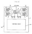
- Fig. 20is a schematic block diagram of such a semiconductor device.
- the semiconductor device 100includes functional circuit (or internal circuit) 110 and a substrate bias generating circuit 120 formed on a single semiconductor substrate.
- the functional circuit 110is constituted by a number of MOS transistors for implementing functions necessary for the semiconductor device 100.
- the substrate bias generating circuit 120is also constituted by MOS transistors and it generates a substrate bias voltage V BB for maintaining the semiconductor substrate 1 at a predetermined negative potential.
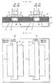
- Fig. 21is a cross sectional view showing a portion of a cross sectional structure of a general integrated circuit device.
- the functional circuit 110 shown in Fig. 20includes the sectional structure shown in Fig. 21.
- Fig. 21shows, as an example, an NMOS transistor and interconnections provided in the periphery thereof.
- the NMOS transistorincludes N type impurity regions 2 and 3 serving as source and drain formed near the main surface of the semiconductor substrate 1 and a gate electrode 5.
- a gate dielectric thin film 4is formed between the gate electrode 5 and the substrate 1.
- P type impurities of low concentration(for example 10 16 to 10 17 /cm 3 ) are introduced to the silicon substrate 1 below the gate electrode 5.
- N type impurities of high concentration(for example, 10 19 to 10 21 /cm 3 ) are introduced to the source region 2 and the drain region 3.
- Interconnection layers 22 and 23 having low resistanceare connected through contact holes formed in an interlayer insulating film 24 to the gate electrode 5, the source region 2 and to the drain region 3.
- N type carriersare induced at an upper layer portion of the silicon substrate 1 of P - region. More specifically, the surface of the silicon substrate 1 is inverted to N type, so that the surface of the silicon substrate 1 has the same type of conductivity as that of the source region 2 and the drain region 3. Thus it becomes possible for a current to flow between the drain region and source region.
- the concentration of the N type carriers induced on the surface of the silicon substrate 1changes dependent on the voltage applied to the gate electrode 5, and therefore the amount of current flowing between the source region 2 and the drain region 3 can be controlled by the gate voltage.
- PN junctionsare formed between the P type silicon substrate 1 and the source region 2 and between the substrate 1 and the drain region 3, the PN junctions are brought to the forward bias state. Accordingly, leak current flows between the silicon substrate 1 and the source region 2 and the drain region 3. Consequently, there is a possibility that the channel is not formed between the source region 2 and the drain region 3, or that the signal to be transmitted is delayed.
- the substrate bias generating circuit 120for keeping the potential V BB of the substrate 1 at about -1V, for example, is provided.
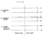
- Fig. 22shows the threshold voltages and the drivability of supplying current when the substrate bias potential is set at -1V.
- the solid linesrepresent the threshold voltage and the drivability of supplying current when the substrate bias potential is at -1V.
- (a)represents the substrate bias potential
- (b)represents the threshold voltages of the NMOS transistor
- (c)represents the drivability of supplying current of the NMOS transistor.
- a constant substrate biasis applied (in Fig. 22, - 1V) to the silicon substrate 1 no matter whether it is in an active state or in a standby state.
- the threshold voltagechanges in the negative direction when the substrate bias changes in the positive direction.
- the drivability of supplying currentalso changes.
- the threshold voltage changes in the negative directionthe drivability of supplying current increases
- the threshold voltage changes in the positive directionthe drivability of supplying current increases.
- a constant substrate biasis applied, and therefore the threshold voltage and the current supplying drivability do not change as shown in Fig. 22.
- the conventional semiconductor deviceis structured as described above, when the threshold voltage is set to minimize the leak current in the standby state, the drivability of supplying current at the active state becomes small, which prevents high speed operation.
- Japanese Patent Laying-Open No. 3-29183discloses a semiconductor memory device in which substrate potential is switched between an active state and a standby state and in which a deeper substrate bias voltage is applied at the standby state than at the active state.
- Fig. 23is a block diagram showing the device for switching the substrate bias disclosed in the aforementioned article.
- this deviceincludes an identifying circuit 101 for identifying the active mode and the standby mode; a substrate potential generating circuit 102 having large current drivability for generating a second substrate potential at the active state; a substrate potential generating circuit 103 having smaller current drivability for generating a first substrate potential causing deeper reverse bias than the second substrate potential at the standby state; a comparing circuit 104 for comparing the substrate potential and a reference potential corresponding to the second substrate potential; a comparing circuit 105 for comparing the substrate potential with a reference potential corresponding to the first substrate potential; and a control portion 106 for selecting one of the substrate potential generating circuits 102 and 103 in response to an output signal from the identifying circuit 101 and maintaining constant the substrate potential generated by the selected substrate potential generating circuit in response to output signals from the comparing circuits 104 and 105.
- the current drivability of the substrate potential generating circuit 102is smaller than that of the circuit 103, since, at the standby state, the first substrate potential is generated only to prevent dissipation of the data stored in the memory cell.
- the current drivabilityis small, there is a possibility that the PN junction is set to the forward biased state by the external noise.
- the first substrate potentialis set to a potential providing deep reverse bias.
- the second substrate potentialis made to provide shallower bias than the first substrate potential, since at the active state, there is an internal signal (for example, word lines of the memory) which is raised to be higher than the supply voltage and when the same reverse bias as the first substrate potential is applied, there is a possibility that the breakdown voltage of the PN junction is exceeded.
- identifying circuit 101recognizes that it is the active mode, and let control portion 106 control in a manner corresponding to the active mode.
- Control portion 106controls the substrate potential generating circuit 102 in response to the output from comparing circuit 104 and maintains the voltage of the substrate at the second substrate potential.
- identifying circuit 101recognizes that it is the standby mode, and let the control portion 106 control in the manner corresponding to the standby mode.
- Control portion 106controls substrate potential generating circuit 103 in response to the output from comparing circuit 105 and maintains the substrate potential at the first substrate potential.
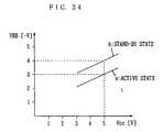
- Fig. 24is a graph showing an example of the relation between the supply voltage Vcc and the first and second substrate potentials b and a generated by the device shown in Fig. 23.
- the supply voltage Vccis at 5V
- the first substrate potential bis - 4V
- the second substrate potential ais -3V.
- the voltage (-3V) of the second substrate potentialis similar to the substrate potential of the conventional general semiconductor device, and it is determined based on the relation with respect to the impurity concentration doped in the substrate.
- the speed of operation of the semiconductor deviceis approximately the same as that in the conventional general semiconductor device, and therefore, the speed of operation of the transistor can not be expected to be faster in the active state.
- the semiconductor memory deviceIn order to increase the speed of operation of the semiconductor memory device, it is necessary to determine the voltage of the substrate potential taking into consideration the current drivability and the threshold voltage of the MOS transistor internally provided. Further, it is necessary to determine the first substrate potential taking into consideration the relation between the threshold voltage and the current drivability.
- the present inventionwas made to solve the above described problem and its object is to provide a semiconductor device in which current consumption in the standby state can be made smaller and the speed of operation in the active state can be increased.
- the semiconductor device of the present inventionis specified by claim 1.
- the semiconductor deviceincludes a buried insulator layer formed on a semiconductor substrate, a semiconductor layer formed on the buried insulator layer, and a CMOS circuit including MOS transistors of the first and second conductivity types formed on the semiconductor layer.
- the semiconductor devicefurther includes a first region, a second region, first to fourth bias voltage generating devices and a bias voltage supplying device. The first region is provided in the buried insulator layer below the MOS transistor of the first conductivity type.
- the second regionis provided in the buried insulator layer below the MOS transistor of the second conductivity type.
- the first bias voltage generating devicegenerates a first bias voltage for determining the magnitude of leak current in the inactive state of the MOS transistor of the first conductivity type.
- the third bias voltage generating devicegenerates a third bias voltage for minimizing the magnitude of leak current in the inactive state of the MOS transistor of the second conductivity type.
- the second bias voltage generating devicegenerates a second bias voltage for maximizing the drivability of supplying current in the active state of the MOS transistor of the first conductivity type, with the bias made shallower than the first bias voltage.
- the fourth bias voltage generating devicegenerates a fourth bias voltage for maximizing the drivability of supplying current in the active state of the MOS transistor of the second conductivity type, with the bias made shallower than the third bias voltage.
- the bias voltage supplying devicesupplies, instead of the first bias voltage, the second bias voltage to the first region, and supplies, instead of the third bias voltage, the fourth bias voltage to the second region, in response to a signal for making active the CMOS circuit.
- first and second regionsare formed in the buried insulator layer in accordance with the third aspect described above, and various voltages are supplied to the first and second regions.
- first bias voltageto the first region and the third bias voltage to the second region
- biases of the MOS transistorsare made shallower, the magnitude of leak current in the standby state is reduced, and accordingly, power consumption can be reduced.
- second bias voltageto the first region and fourth bias voltage to the second region
- the biases of the MOS transistorsare made shallower, and accordingly, the speed of operation in the active state can be increased.
- Fig. 1is a block diagram showing a semiconductor device useful for understanding the invention.
- Fig. 2is a cross section of a portion of the semiconductor device shown in Fig. 1.
- Fig. 3is an illustration showing changes of the threshold voltage and the drivability of supplying current when the substrate bias is switched.
- Fig. 4Ais a graph showing relation between substrate bias and power consumption.
- Fig. 4Bshows a change in I D - V G characteristic incidental to the change in the substrate bias.
- Fig. 5Ashows a change in I D - V D characteristic incidental to the change in the substrate bias.
- Fig. 5Bshows improvement of the speed of operation with respect to the change in the substrate bias.
- Fig. 6is a schematic diagram showing an example of the first bias generating circuit shown in Fig. 1.
- Fig. 7Ais a block diagram showing an example of the second bias generating circuit shown in Fig. 1.
- Fig. 7Bis a block diagram showing another example of the second bias generating circuit shown in Fig. 1.
- Fig. 8is a schematic diagram showing an example of the bias selecting circuit shown in Fig. 1.
- Fig. 9is a block diagram of another semiconductor device useful for understanding the invention.
- Fig. 10is a cross section of a portion of the semiconductor device shown in Fig. 9.
- Fig. 11is a plan view showing a portion of the semiconductor device shown in Fig. 9.
- Fig. 12shows changes in the substrate bias, the threshold voltage and the drivability of supplying current when the semiconductor device of Fig. 9 is switched from the standby state to the active state.
- Fig. 13is a schematic diagram showing an example of the bias selecting circuit shown in Fig. 9.
- Fig. 14is a cross section showing an embodiment of the semiconductor device in accordance with the present invention.
- Fig. 15shows changes in the substrate bias, the threshold voltage and the drivability of supplying current when the semiconductor device of Fig. 14 is switched from the standby state to the active state.
- Fig. 16is a cross sectional view showing a further embodiment of the semiconductor device in accordance with the present invention.
- Fig. 17is a plan view of the semiconductor device shown in Fig. 16.
- Fig. 18shows changes in the substrate bias, the threshold voltage and the drivability of supplying current when the device is switched from the standby state to the active state.
- Fig. 19shows a step of forming the SOI structure shown in Fig. 16.
- Fig. 20is a block diagram showing an example of a conventional semiconductor device.
- Fig. 21is a cross section of a portion of the semiconductor device shown in Fig. 20.
- Fig. 22is a diagram showing a method of supplying substrate bias in the semiconductor device shown in Fig. 20.
- Fig. 23shows a conventional substrate bias switching device.
- Fig. 24shows the substrate potential-supply voltage characteristic of the device shown in Fig. 23.
- Fig. 1is a block diagram showing a semiconductor device useful for understanding the invention.
- the semiconductor device 200includes a functional circuit 110, a first bias generating circuit 30, a second bias generating circuit 31 and a bias selecting circuit 32 formed on a single silicon substrate 1.
- the functional circuit 110is the same as that shown in Fig. 20.
- the first bias generating circuit 30generates a substrate bias VBB1 in the standby state.
- the substrate bias VBB1is determined such that the threshold voltage Vth of the NMOS transistor is set to 0.8V.
- the potential of the substrate bias VBB1is related with the drivability of supplying current (mutual conductance) of the NMOS transistor.
- VBB1is about -3V.
- the second bias generating circuit 31generates a substrate bias VBB2 in the active state.
- the substrate bias VBB2is determined based on the drivability of supplying current in the active state of the NMOS transistor.
- the drivability of supplying currentbecomes larger as the threshold voltage Vth becomes smaller, and the drain current flows more easily.
- the substrate bias VBB2is 0V and the threshold voltage Vth is 0.2V, and the current supplying drivability is increased by about 30% than the drivability in the standby state.
- the bias selecting circuit 32is connected to the first and second bias generating circuits 30 and 31 and it selects the substrate bias VBB2 generated by the second bias generating circuit 31 in response to a control signal CNT, and applies this to the silicon substrate 1.
- Fig. 2is a cross section of a portion of the semiconductor device shown in Fig. 1.
- the semiconductor device shown in Fig. 2differs from the semiconductor device of Fig. 21 in that the substrate bias VBB1 or VBB2 is supplied to the rear surface of the silicon substrate 1.
- the substrate bias VBB1is -3V, and the source region 2 and the drain region 3 of the silicon substrate 1 are deeply reverse-biased.
- Fig. 3shows changes in the threshold voltage and the drivability of supplying current when the substrate bias is switched from VBB1 to VBB2.
- Fig. 4Ais a graph showing the relation between the substrate bias and power consumption.
- Fig. 4Bshows changes in the I D - V G characteristic incidental to the change of the substrate bias.
- Fig. 5Ashows changes in the I D - V D characteristic incidental to the change of the substrate bias.
- the substrate bias VBB1is determined mainly based on the relation between the power consumption of the first bias generating circuit 30 itself and the amount of leak current.
- the dotted linerepresents power consumption when the substrate bias VBB1 generated by the first bias generating circuit 30 is changed
- one-dotted linerepresents the magnitude of leak current when the substrate bias VBB1 is changed.
- the power consumption at the standby statecorresponds to the sum (the solid line of Fig. 4A) of the power consumption by the first bias generating circuit 30 itself and the power consumption caused by the leak current.
- the most suitable substrate biasis -3V at which the sum of the power consumption becomes minimum.
- the threshold voltage Vthis lowered to 0.2V so as to reduce the ratio of the threshold voltage Vth with respect to the supply voltage Vcc, and thus the speed of operation can be improved.
- the value of 0Venables increase of drivability of the transistor at the active state.
- the gate lengthis 0.8 ⁇ m, and in a 3V system, the gate length is 0.5 ⁇ m. In a 1.5V system which will be manufactured in the future, the gate length is expected to be 0.15 ⁇ m.
- the threshold voltage at the standby stateis constant because of the transistor characteristic, and therefore in the 1.5V system, even when Vth can be reduced to 0.5V, the ratio of the threshold voltage Vth with respect to the operating voltage will be as high as 33%. Therefore, the method of reducing the threshold voltage by changing the substrate bias shown in Fig. 4B becomes very effective.
- the solid linerepresents the I D - V D characteristic when the substrate bias VBB(-3V) is supplied, while the dotted line represents the I D - V D characteristic when the substrate bias VBB2(0V) is supplied. From this figure, it can be seen that the speed of rise is improved when the substrate bias VBB2 is supplied as shown in Fig. 5B.
- the substrate bias VBB1is supplied to the silicon substrate 1, the threshold voltage Vth is 0.8V, and the current supplying drivability is 100% as in the conventional example.
- the silicon substrate 1, the source region 2 and the drain region 3are deeply reverse-biased, which can minimize the amount of leak current.
- the bias selecting circuit 32selects the substrate bias VBB2 instead of the substrate bias VBB1. Consequently, the reverse-bias between the silicon substrate 1 and the source region 2, and between the substrate and the drain region 3 becomes shallower, the threshold voltage Vth attains to 0.2V, the current supplying drivability is increased to about 130%, and the resistance between the drain region and the source region is made smaller.
- the channel regionis quickly inverted to the N type, which increases the speed of operation.
- NMOS transistoris used in the embodiment shown in Figs. 1 to 5, the similar operation is done in a PMOS transistor. More specifically, if the substrate bias is reduced from 8V to 5V and the threshold voltage is changed from 4.2V to 4.8V, the drivability of supplying current is improved and the speed of operation is increased. This correspond to an example in which a supply voltage in the rage of 0 to 5V is used. If a supply voltage in the rage of -5 to 0V is used, the change of the substrate bias is 3V to 0V, and the threshold voltage changes from -0.8V to -0.2V. More specifically, in the PMOS transistor, the substrate bias changes in the direction of the drain bias, as viewed from source bias. The change of the threshold voltage is in the direction of the source bias.
- Fig. 6is a schematic diagram showing the first bias generating circuit shown in Fig. 1.
- the first bias generating circuit 30includes a ring oscillator 301 and a charge pump circuit 302.
- the ring oscillator 301includes a plurality of cascade connected invertors 303, 304 and 305.
- the ring oscillator 301oscillates when the output is fed back to the input, and generates a signal of a prescribed frequency.
- the charge pump circuit 302includes a driver 306, capacitors 307 and 310, and diodes 308 and 309.
- the driver 306amplifies the signal of a prescribed period from the ring oscillator 301 and applies the amplified signal to one end of the capacitor 307.
- the substrate bias VBB1attains -Vcc + Vth, where Vth is the threshold voltage of the diode 308.
- Fig. 7A and Fig. 7Bare schematic diagrams showing examples of the second bias generating circuit 31 shown in Fig. 1.
- the circuitdiffers from that of Fig. 6 in that a diode 313 is added to the charge pump circuit 312.
- the substrate bias VBB2is made to have a desired potential (-1V to 0V) by increasing the number of diodes.
- the substrate bias generating circuit 31includes a ground terminal GND and an interconnection 31a connected between the ground terminal GND and a substrate bias output terminal VBB2.
- the substrate bias (0V) at the active statecan be generated by the simplest structure.
- Fig. 8is a schematic diagram showing an example of the bias selecting circuit 32 shown in Fig. 1.
- the bias selecting circuit 32includes NMOS transistors 321 and 322.
- the NMOS transistor 321has its source connected to receive the substrate bias VBB1, its drain connected to the silicon substrate 1 together with the drain of the NMOS transistor 322, and its gate connected to receive the control signal /CNT.
- the NMOS transistor 322has its source connected to receive the substrate bias VBB2, and its gate connected to receive the signal CNT.
- the control signal /CNTis set to the high level, NMOS transistor 321 is turned on, and the substrate bias VBB1 is supplied to the silicon substrate 1.
- the control signal CNTis set to the high level, the NMOS transistor 322 is turned on, and the substrate bias VBB2 is supplied to the silicon substrate 1.
- the substrate biasis changed in response to the control signal CNT.
- input signals Din and /Dinmay be applied to the gates of the NMOS transistors 321 and 322.
- Fig. 9is a block diagram of another semiconductor device useful for understanding the invention.
- the semiconductor devicediffers from the semiconductor device of Fig. 1 in that a CMOS circuit is included in the functional circuit 110, the third and fourth substrate bias circuits 33 and 34 are added, and a bias selecting circuit 32' for selecting the substrate bias VBB2 or VBB4 are provided.
- Other circuitsare the same as those shown in Fig. 1, and therefore they are denoted by the same reference numerals and description thereof is not repeated.
- the third bias generating circuit 33generates a substrate bias VBB3 in the standby state of the PMOS transistor.
- the substrate bias VBB3is set at such a potential as to set the threshold voltage (Vth) of the PMOS transistor at 4.2V. Specifically, it is about 8V. By making this such a deep reverse bias, the leak current in the standby state can be reduced.
- the fourth bias generating circuit 34generates a substrate bias VBB4 in the active state of the PMOS transistor.
- the substrate bias VBB4is determined based on the drivability of supplying current in the active state of the PMOS transistor. More specifically, it is 5V. The drivability of supplying current becomes larger when the threshold voltage Vth is smaller. By determining the threshold voltage, the gate width and the gate length, the current supplying drivability is determined. In this embodiment, the substrate bias VBB4 is set to 5V and the threshold voltage is set to 4.8V, thus increasing the supplying drivability by about 30%.
- Fig. 10is a cross section of a portion of the semiconductor device shown in Fig. 9.
- Fig. 11is a plan view showing a portion of the semiconductor device shown in Fig. 9.
- the semiconductor device shown in Figs. 10 and 11constitutes a CMOS circuit including an NMOS transistor and a PMOS transistor combined. Referring to Figs.
- the semiconductor deviceincludes a P well 6 doped with P type impurities of 10 16 to 10 17 /cm 3 on a silicon substrate 1, an NMOS transistor 11 formed on the P well 6, an N well 10 doped with N type impurities of 10 16 to 10 17 /cm 3 , for example, a PMOS transistor 12 formed on the N well 10, a well terminal 26 to which the substrate bias VBB1 or VBB2 is supplied, and a well terminal 27 to which the substrate bias VBB3 or VBB4 is supplied.
- the well terminal 26is connected to the contact hole 26' shown in Fig. 11, and the well terminal 27 is connected to the contact hole 27' shown in Fig. 11.
- Fig. 12shows changes in the substrate bias (well bias), the threshold voltage and the drivability of supplying current when the semiconductor device shown in Fig. 9 is switched from the standby state to the active state.
- the well bias VBB1is supplied to the well terminal 26 and the well bias VBB3 is supplied to the well terminal 27, and therefore the threshold voltages Vth are 0.8V and 4.2V, and the drivability of supplying current is 100% as in the prior art.
- the P well 6 and the source region 2 and the drain region 3are in the deeply reverse-biased state, and the N well 10 and the source region 8 and the drain region 9 are in the deeply reverse-biased state.
- the amount of currentcan be made very small.
- the signal CNTis supplied to the bias selecting circuit 32'.
- the bias selecting circuit 32'selects the substrate bias VBB2 instead of the substrate bias VBB1 to apply this to the well terminal 6, selects the substrate bias VBB4 instead of the substrate bias VBB3 and applies this to the well terminal 27. Consequently, the reverse bias between the P well 6 and each of the source and drain regions 2 and 3 as well as the reverse bias between the N well 10 and each of the source and drain regions 8 and 9 are made shallower. Consequently, the threshold voltages Vth are set to 0.2V and 4.8V, the current supplying drivability is increased to about 130%, and the resistance between the drain region and the source region is made smaller.
- Fig. 13is a schematic diagram showing an example of the bias selecting circuit 32' shown in Fig. 9.
- the bias selecting circuit 32'differs from the bias selecting circuit 32 shown in Fig. 8 in that an NMOS transistor 323 responsive to the control signal /CNT for selecting the substrate bias VBB3, and an NMOS transistor 324 responsive to the control signal CNT for selecting the substrate bias VBB4 are added.
- Other portionsare the same as those in Fig. 8.
- Fig. 14is a cross section showing an embodiment of the semiconductor device in accordance with the present invention.
- the semiconductor device shown in Fig. 14has a so called SOI structure.
- the semiconductor deviceincludes a buried insulator layer 14 formed on a silicon substrate 15, an NMOS transistor 11 formed on the buried insulator layer 14, and a PMOS transistor 12 formed on the buried insulator layer 14.
- SOI-MOSFETis formed by the SIMOX (Separation by Implanted Oxygen).
- 2 x 10 18 /cm 2 of oxygen ionsare implanted to the silicon substrate 15 and thereafter it is heat treated at 1300°C for 6 hours in Ar atmosphere to provide an SOI substrate including three layered structure of silicon/silicon oxide film/silicon.
- the silicon layer 13is processed to be islands, and is divided into the NMOS transistor 11 and the PMOS transistor 12.
- a gate electrode 5is provided with a gate dielectric thin film 4 interposed as in the conventional device formed on the silicon substrate.
- an N channel region 16 doped with P type impurities of 10 16 to 10 17 /cm 3is provided in the silicon layer 13 below the gate electrode 5, and the source and drain regions 2 and 3 are provided in the similar manner as the prior art on both sides of the N channel region 16.
- the N channel region 16is completely depleted, and the impurity concentration of the N channel region 16 is suppressed low, as mentioned above.
- the impurity concentration of the P channel region 17is made not lower than 10 17 /cm 3 , which is higher than the NMOS transistor 11, and even when the gate voltage is applied, only a portion of the P channel region 17 is depleted. Except this, the PMOS transistor has similar structure as the NMOS transistor, with the type of impurities opposite to that of NMOS transistor.
- the substrate biases VBB1 and VBB2are supplied from the rear surface of the silicon substrate 1.
- the substrate bias VBB1is fixed at 0V so as to set the threshold voltage Vth at 0.8V
- the potential of the substrate bias VBB2is 5V so as to set the threshold voltage Vth at 0.2V.
- Fig. 15shows changes in the threshold voltage and the drivability of supplying current when the substrate bias is changed.
- the SOI-MOSFEThas a MOS structure of silicon substrate 15 / buried oxide layer 14 / silicon layer 13, as viewed from the side of the silicon substrate 15.
- MOS structureis formed on both surfaces of the silicon layer 13.
- the operation when the substrate bias VBB2 (5V) is applied from the silicon substrate 15changes dependent on whether the channel region is completely depleted or partially depleted when the voltage is applied to the gate.
- the capacitorsare coupled in series from the buried oxide film 14 to the gate dielectric thin film 4 (buried oxide layer 14 / silicon layer 13 / gate dielectric thin film 4) (capacitance coupled), and the threshold voltages of the MOS transistors 11 and 12 on the top surface side are changed by the substrate bias.
- the direction of change of the threshold voltages caused by the substrate bias changeis the same as that of the MOS transistor formed on the bulk silicon described above. However, since the bias potential is supplied to the semiconductor layer 13 through the thick buried oxide layer 14, the change becomes smaller.
- the channel regionis partially depleted, that is, the case of the PMOS transistor.
- the potential of the channel region which is not depletedis fixed at the potential of the source region 8. Therefore, such a capacitance coupling as occurred when it is fully depleted is not generated. Therefore, the threshold voltage of the MOS on the surface is not influenced by the normal back gate bias.
- the back gate bias VBB1(substrate bias) is fixed at 0V, and the threshold value is set to suppress current in this state. Thus power consumption can be reduced.
- the threshold value of the NMOS transistor 11decreases from 0.8V to 0.2V, and hence the drivability of supplying current is increased. By this increase of current, the circuit can operate at higher speed.
- the channel regionis partially depleted, and therefore there is no effect of back gate bias, and the threshold value and the drivability of supplying current are not changed.
- the PMOS transistor 12is depleted partially so that it is not influence by the back gate bias, since if the NMOS transistor and the PMOS transistor are both fully depleted to be subjected to the back gate bias effect in the SOI-MOSFET, the effects increasing current is reversed in the NMOS transistor and the PMOS transistor. That is, if the back gate bias is applied to increase the current in the NMOS transistor, the drivability of supplying current in the PMOS transistor is reduced.
- the NMOS transistoris fully depleted and the PMOS transistor is partially depleted.
- the reverse combinationmay be available, dependent on the circuit structure.
- the back gate biassubstrate bias
- the back gate biasmust be changed in the negative direction, that is, from 5V to 0V, for example.
- Fig. 16is a cross section showing a further embodiment of the semiconductor device in accordance with the present invention
- Fig. 17is a plan view of the semiconductor device shown in Fig. 16.
- the NMOS transistor and the PMOS transistorare both fully depleted.
- the semiconductor devicediffers from the semiconductor device shown in Fig. 14 in that an NMOS second gate 18 and a PMOS second gate 19 are provided in the buried oxide film layer.
- the NMOS second gate 18is provided below the silicon layer 13 of the NMOS transistor 11, and the PMOS second gate 19 is provided below the PMOS transistor 12.
- a substrate terminal 28 for receiving substrate biases VBB1 and VBB2 and a substrate terminal 29 for receiving mutually complementary substrate biases VBB1 and VBB2are provided on the silicon layer 13.
- the potentials of the substrate biases VBB1 and VBB2are the same as in the embodiment of Fig. 14 (0V, 5V).
- Fig. 18shows changes in the threshold voltage and the drivability of supplying current when the substrate bias is changed.
- the substrate bias VBB1 (0V)is supplied to the NMOS second gate 18 and the substrate bias VBB2 (5V) is supplied to the PMOS second gate 19 in the standby state.
- the substrate biasesBy the application of the substrate biases, the threshold voltage Vth of the NMOS transistor 11 attains 0.8V, and the threshold voltage Vth of the PMOS transistor 12 attains 4.2V, resulting in a deep reverse bias.
- the operation so faris the same as that of the embodiment shown in Fig. 14.
- the substrate bias VBB2is supplied to the NMOS second gate 18, while the substrate bias VBB1 is supplied to the PMOS second gate 19.
- the threshold voltage of the NMOS transistor 11attains 0.2V
- the threshold voltage of the PMOS transistor 12attains 4.8V.
- the drivability of supplying current in the MOS transistors 11 and 12is increased to about 130%, and consequently, the speed of operation of the CMOS circuit can be increased.
- Fig. 19shows steps for manufacturing the SOI structure shown in Fig. 16.
- a silicon oxide filmis formed on the silicon substrate 15, and thereafter a polysilicon layer as the second gates 18 and 19 are formed by sputtering or the like.
- the silicon layer 40is deposited.
- siliconwas used for the semiconductor in the embodiments shown in Figs. 1 to 19, other semiconductor material such as germanium Ge or gallium arsenide GaAs may be used.
Landscapes
- Engineering & Computer Science (AREA)
- Computer Hardware Design (AREA)
- Physics & Mathematics (AREA)
- Computing Systems (AREA)
- General Engineering & Computer Science (AREA)
- Mathematical Physics (AREA)
- Power Engineering (AREA)
- Microelectronics & Electronic Packaging (AREA)
- Dram (AREA)
- Semiconductor Integrated Circuits (AREA)
- Logic Circuits (AREA)
Description
- The present invention relates to a semiconductordevice including a MOS (Metal Oxide Semiconductor) fieldeffect transistor (hereinafter referred to as "MOSFET")formed on a semiconductor substrate and, moreparticularly, to an improvement in supplying a substratebias voltage.
- Generally, a semiconductor device such as a dynamicrandom access memory and a static random access memory isconstituted by a number of MOS transistors formed on onesemiconductor substrate. Normally, the potential of thesemiconductor substrate is constantly maintained in apredetermined range in such a semiconductor device.
- Fig. 20 is a schematic block diagram of such asemiconductor device. Referring to Fig. 20, the
semiconductor device 100 includes functional circuit (orinternal circuit) 110 and a substratebias generatingcircuit 120 formed on a single semiconductor substrate.Thefunctional circuit 110 is constituted by a number ofMOS transistors for implementing functions necessary forthesemiconductor device 100. The substratebias generating circuit 120 is also constituted by MOStransistors and it generates a substrate bias voltage VBBfor maintaining thesemiconductor substrate 1 at apredetermined negative potential. - Fig. 21 is a cross sectional view showing a portionof a cross sectional structure of a general integratedcircuit device. The
functional circuit 110 shown in Fig.20 includes the sectional structure shown in Fig. 21.Fig. 21 shows, as an example, an NMOS transistor andinterconnections provided in the periphery thereof.Referring to Fig. 21, the NMOS transistor includes Ntypeimpurity regions semiconductorsubstrate 1 and agate electrode 5. A gate dielectricthin film 4 is formed between thegate electrode 5 and thesubstrate 1. P type impurities of low concentration (forexample 1016 to 1017/cm3) are introduced to thesiliconsubstrate 1 below thegate electrode 5. N type impuritiesof high concentration (for example, 1019 to 1021/cm3) areintroduced to thesource region 2 and thedrain region 3.Interconnection layers interlayerinsulating film 24 to thegate electrode 5, thesourceregion 2 and to thedrain region 3. - In the MOS transistor formed as described above, when a positive voltage is applied to the
gate electrode 5, Ntype carriers (electrons) are induced at an upper layerportion of thesilicon substrate 1 of P- region. Morespecifically, the surface of thesilicon substrate 1 isinverted to N type, so that the surface of thesiliconsubstrate 1 has the same type of conductivity as that ofthesource region 2 and thedrain region 3. Thus itbecomes possible for a current to flow between the drainregion and source region. The concentration of the N typecarriers induced on the surface of thesilicon substrate 1changes dependent on the voltage applied to thegateelectrode 5, and therefore the amount of current flowingbetween thesource region 2 and thedrain region 3 can becontrolled by the gate voltage. - In operation, when the NMOS transistor is renderedconductive, hot electrons and holes which constitute pairsare generated near the
drain region 3. Most of thegenerated hot electrons flow to thedrain region 3.Meanwhile, most of the generated holes flow to thesiliconsubstrate 1. Thus the potential of thesilicon substrate 1 rises. The rise of the potential of thesiliconsubstrate 1 causes the following problem. - Since PN junctions are formed between the P
typesilicon substrate 1 and thesource region 2 and betweenthesubstrate 1 and thedrain region 3, the PN junctions are brought to the forward bias state. Accordingly, leakcurrent flows between thesilicon substrate 1 and thesource region 2 and thedrain region 3. Consequently,there is a possibility that the channel is not formedbetween thesource region 2 and thedrain region 3, orthat the signal to be transmitted is delayed. - In order to prevent the above problem, the substrate
bias generating circuit 120 for keeping the potential VBBof thesubstrate 1 at about -1V, for example, is provided. - The conventional operation for supplying substratebias will be described with reference to Fig. 22. Fig. 22shows the threshold voltages and the drivability ofsupplying current when the substrate bias potential is setat -1V. Referring to Fig. 22, the solid lines representthe threshold voltage and the drivability of supplyingcurrent when the substrate bias potential is at -1V. Inthe figure, (a) represents the substrate bias potential,(b) represents the threshold voltages of the NMOStransistor and (c) represents the drivability of supplyingcurrent of the NMOS transistor.
- A constant substrate bias is applied (in Fig. 22, -1V) to the
silicon substrate 1 no matter whether it is inan active state or in a standby state. The thresholdvoltage changes in the negative direction when thesubstrate bias changes in the positive direction. By the change of the threshold voltage, the drivability ofsupplying current also changes. In the NMOS transistor,when the threshold voltage changes in the negativedirection, the drivability of supplying current increases,while in a PMOS transistor, when the threshold voltagechanges in the positive direction, the drivability ofsupplying current increases. However, in the conventionalmethod of supplying the substrate bias, a constantsubstrate bias is applied, and therefore the thresholdvoltage and the current supplying drivability do notchange as shown in Fig. 22. - Since the conventional semiconductor device isstructured as described above, when the threshold voltageis set to minimize the leak current in the standby state,the drivability of supplying current at the active statebecomes small, which prevents high speed operation.
- Conversely, if the drivability of supplying currentis increased and the threshold value is lowered in orderto operate the NMOS transistor at high speed, the leakcurrent in the standby state increases.
- Now, Japanese Patent Laying-Open No. 3-29183discloses a semiconductor memory device in which substratepotential is switched between an active state and astandby state and in which a deeper substrate bias voltageis applied at the standby state than at the active state.
- Fig. 23 is a block diagram showing the device forswitching the substrate bias disclosed in theaforementioned article. Referring to Fig. 23, this deviceincludes an identifying
circuit 101 for identifying theactive mode and the standby mode; a substratepotentialgenerating circuit 102 having large current drivabilityfor generating a second substrate potential at the activestate; a substratepotential generating circuit 103 havingsmaller current drivability for generating a firstsubstrate potential causing deeper reverse bias than thesecond substrate potential at the standby state; acomparingcircuit 104 for comparing the substratepotential and a reference potential corresponding to thesecond substrate potential; acomparing circuit 105 forcomparing the substrate potential with a referencepotential corresponding to the first substrate potential;and acontrol portion 106 for selecting one of thesubstratepotential generating circuits circuit 101 and maintaining constant the substrate potentialgenerated by the selected substrate potential generatingcircuit in response to output signals from thecomparingcircuits - The current drivability of the substrate
potentialgenerating circuit 102 is smaller than that of thecircuit 103, since, at the standby state, the first substratepotential is generated only to prevent dissipation of thedata stored in the memory cell. However, since thecurrent drivability is small, there is a possibility thatthe PN junction is set to the forward biased state by theexternal noise. In order to prevent the forward biasedstate, the first substrate potential is set to a potentialproviding deep reverse bias. - In this prior art, the second substrate potential ismade to provide shallower bias than the first substratepotential, since at the active state, there is an internalsignal (for example, word lines of the memory) which israised to be higher than the supply voltage and when thesame reverse bias as the first substrate potential isapplied, there is a possibility that the breakdown voltageof the PN junction is exceeded.
- In operation, when a signal designating the activemode is input externally, identifying
circuit 101recognizes that it is the active mode, and letcontrolportion 106 control in a manner corresponding to theactive mode.Control portion 106 controls the substratepotential generating circuit 102 in response to the outputfrom comparingcircuit 104 and maintains the voltage ofthe substrate at the second substrate potential. - Meanwhile, when a signal designating the standby mode is input externally, identifying
circuit 101 recognizesthat it is the standby mode, and let thecontrol portion 106 control in the manner corresponding to the standbymode.Control portion 106 controls substrate potentialgeneratingcircuit 103 in response to the output fromcomparingcircuit 105 and maintains the substratepotential at the first substrate potential. By doing so,the reverse bias at the standby state can be made deeperthan the reverse bias at the active state, and thereforedissipation of data stored in the memory cell in thestandby state can be prevented. - Fig. 24 is a graph showing an example of the relationbetween the supply voltage Vcc and the first and secondsubstrate potentials b and a generated by the device shownin Fig. 23. As is apparent from Fig. 24, when the supplyvoltage Vcc is at 5V, the first substrate potential b is -4V and the second substrate potential
a is - 3V. Thevoltage (-3V) of the second substrate potential is similarto the substrate potential of the conventional generalsemiconductor device, and it is determined based on therelation with respect to the impurity concentration dopedin the substrate. - Therefore, the speed of operation of thesemiconductor device is approximately the same as that inthe conventional general semiconductor device, and therefore, the speed of operation of the transistor cannot be expected to be faster in the active state.
- In order to increase the speed of operation of thesemiconductor memory device, it is necessary to determinethe voltage of the substrate potential taking intoconsideration the current drivability and the thresholdvoltage of the MOS transistor internally provided.Further, it is necessary to determine the first substratepotential taking into consideration the relation betweenthe threshold voltage and the current drivability.
- The prior art shown in Fig. 23 is silent about theserelations.
- The present invention was made to solve the abovedescribed problem and its object is to provide asemiconductor device in which current consumption in thestandby state can be made smaller and the speed ofoperation in the active state can be increased.
- Briefly stated, the semiconductor device of thepresent invention is specified by
claim 1. - The semiconductor device according tothe present invention includes a buriedinsulator layer formed on a semiconductor substrate, asemiconductor layer formed on the buried insulator layer,and a CMOS circuit including MOS transistors of the firstand second conductivity types formed on the semiconductorlayer. The semiconductor device further includes a firstregion, a second region, first to fourth bias voltagegenerating devices and a bias voltage supplying device.The first region is provided in the buried insulator layerbelow the MOS transistor of the first conductivity type.
- The second region is provided in the buried insulatorlayer below the MOS transistor of the second conductivity type.
- The first bias voltage generating device generates afirst bias voltage for determining the magnitude of leakcurrent in the inactive state of the MOS transistor of thefirst conductivity type.
- The third bias voltage generating device generates athird bias voltage for minimizing the magnitude of leakcurrent in the inactive state of the MOS transistor of thesecond conductivity type.
- The second bias voltage generating device generates asecond bias voltage for maximizing the drivability ofsupplying current in the active state of the MOStransistor of the first conductivity type, with the biasmade shallower than the first bias voltage.
- The fourth bias voltage generating device generates afourth bias voltage for maximizing the drivability ofsupplying current in the active state of the MOStransistor of the second conductivity type, with the biasmade shallower than the third bias voltage.
- The bias voltage supplying device supplies, insteadof the first bias voltage, the second bias voltage to thefirst region, and supplies, instead of the third biasvoltage, the fourth bias voltage to the second region, inresponse to a signal for making active the CMOS circuit.
- In this aspect of the present invention, first and second regions are formed in the buried insulator layer inaccordance with the third aspect described above, andvarious voltages are supplied to the first and secondregions. By supplying the first bias voltage to the firstregion and the third bias voltage to the second region,biases of the MOS transistors are made shallower, themagnitude of leak current in the standby state is reduced,and accordingly, power consumption can be reduced. Bysupplying the second bias voltage to the first region andfourth bias voltage to the second region, the biases ofthe MOS transistors are made shallower, and accordingly,the speed of operation in the active state can beincreased.
- The objects, features, aspectsand advantages of the present invention will become moreapparent from the following detailed description of thepresent invention when taken in conjunction with theaccompanying drawings.
- Fig. 1 is a block diagram showing asemiconductor device useful for understanding theinvention.
- Fig. 2 is a cross section of a portion of thesemiconductor device shown in Fig. 1.
- Fig. 3 is an illustration showing changes of the threshold voltage and the drivability of supplying currentwhen the substrate bias is switched.
- Fig. 4A is a graph showing relation between substratebias and power consumption.
- Fig. 4B shows a change in ID - VG characteristicincidental to the change in the substrate bias.
- Fig. 5A shows a change in ID - VD characteristicincidental to the change in the substrate bias.
- Fig. 5B shows improvement of the speed of operationwith respect to the change in the substrate bias.
- Fig. 6 is a schematic diagram showing an example ofthe first bias generating circuit shown in Fig. 1.
- Fig. 7A is a block diagram showing an example of thesecond bias generating circuit shown in Fig. 1.
- Fig. 7B is a block diagram showing another example ofthe second bias generating circuit shown in Fig. 1.
- Fig. 8 is a schematic diagram showing an example ofthe bias selecting circuit shown in Fig. 1.
- Fig. 9 is a block diagram of another semiconductor deviceuseful for understanding theinvention.
- Fig. 10 is a cross section of a portion of thesemiconductor device shown in Fig. 9.
- Fig. 11 is a plan view showing a portion of thesemiconductor device shown in Fig. 9.
- Fig. 12 shows changes in the substrate bias, thethreshold voltage and the drivability of supplying currentwhen the semiconductor device of Fig. 9 is switched fromthe standby state to the active state.
- Fig. 13 is a schematic diagram showing an example ofthe bias selecting circuit shown in Fig. 9.
- Fig. 14 is a cross section showing anembodiment of the semiconductor device in accordance withthe present invention.
- Fig. 15 shows changes in the substrate bias, thethreshold voltage and the drivability of supplying currentwhen the semiconductor device of Fig. 14 is switched fromthe standby state to the active state.
- Fig. 16 is a cross sectional view showing a furtherembodiment of the semiconductor device in accordance withthe present invention.
- Fig. 17 is a plan view of the semiconductor deviceshown in Fig. 16.
- Fig. 18 shows changes in the substrate bias, thethreshold voltage and the drivability of supplying currentwhen the device is switched from the standby state to theactive state.
- Fig. 19 shows a step of forming the SOI structureshown in Fig. 16.
- Fig. 20 is a block diagram showing an example of a conventional semiconductor device.
- Fig. 21 is a cross section of a portion of thesemiconductor device shown in Fig. 20.
- Fig. 22 is a diagram showing a method of supplyingsubstrate bias in the semiconductor device shown in Fig.20.
- Fig. 23 shows a conventional substrate bias switchingdevice.
- Fig. 24 shows the substrate potential-supply voltagecharacteristic of the device shown in Fig. 23.
- Fig. 1 is a block diagram showing a semiconductor device useful for understanding theinvention. Referring to Fig. 1, the
semiconductor device 200 includes afunctional circuit 110, a firstbiasgenerating circuit 30, a secondbias generating circuit 31and abias selecting circuit 32 formed on asingle siliconsubstrate 1. - The
functional circuit 110 is the same as that shownin Fig. 20. The firstbias generating circuit 30generates a substrate bias VBB1 in the standby state. Thesubstrate bias VBB1 is determined such that the thresholdvoltage Vth of the NMOS transistor is set to 0.8V. Thepotential of the substrate bias VBB1 is related with thedrivability of supplying current (mutual conductance) of the NMOS transistor. When the gate width W is 10µm andthe gate length L is 1µm, VBB1 is about -3V. By supplyingsuch deep reverse bias, leak current in the standby statecan be minimized. - The second
bias generating circuit 31 generates asubstrate bias VBB2 in the active state. The substratebias VBB2 is determined based on the drivability ofsupplying current in the active state of the NMOStransistor. The drivability of supplying current becomeslarger as the threshold voltage Vth becomes smaller, andthe drain current flows more easily. In other words, bydetermining the threshold voltage Vth, the power supplyvoltage Vdd, the gate width and the gate length, thedrivability of supplying current is also determined. Inthis embodiment, the substrate bias VBB2 is 0V and thethreshold voltage Vth is 0.2V, and the current supplyingdrivability is increased by about 30% than the drivabilityin the standby state. - The
bias selecting circuit 32 is connected to thefirst and secondbias generating circuits bias generating circuit 31 in response to a control signalCNT, and applies this to thesilicon substrate 1. - Fig. 2 is a cross section of a portion of thesemiconductor device shown in Fig. 1. The semiconductor device shown in Fig. 2 differs from the semiconductordevice of Fig. 21 in that the substrate bias VBB1 or VBB2is supplied to the rear surface of the
silicon substrate 1. The substrate bias VBB1 is -3V, and thesource region 2 and thedrain region 3 of thesilicon substrate 1 aredeeply reverse-biased. - Fig. 3 shows changes in the threshold voltage and thedrivability of supplying current when the substrate biasis switched from VBB1 to VBB2. Fig. 4A is a graph showingthe relation between the substrate bias and powerconsumption. Fig. 4B shows changes in the ID - VGcharacteristic incidental to the change of the substratebias. Fig. 5A shows changes in the ID - VD characteristicincidental to the change of the substrate bias.
- Referring to Fig. 4A, the most appropriate voltage ofthe substrate potential VBB1 in an MOS transistor havingthe gate width W of 10µm and the gate length L of 1µm willbe described. The substratebias VBB1 is determined mainly based on the relationbetween the power consumption of the first
bias generatingcircuit 30 itself and the amount of leak current. In Fig.4A, the dotted line represents power consumption when thesubstrate bias VBB1 generated by the firstbias generatingcircuit 30 is changed, and one-dotted line represents themagnitude of leak current when the substrate bias VBB1 is changed. The power consumption at the standby statecorresponds to the sum (the solid line of Fig. 4A) of thepower consumption by the firstbias generating circuit 30itself and the power consumption caused by the leakcurrent. - Therefore, the most suitable substrate bias is -3V atwhich the sum of the power consumption becomes minimum.
- Referring to Fig.4B, the solid line shows the ID - VGcharacteristic when the substrate bias is set to VBB1 (=-3V),while the dotted line represents the ID - VGcharacteristic when the substrate bias is set to VBB2 (=0V). Here, the threshold voltage Vth is defined by thegate voltage when a drain current of 10-6A flows. Sincethe magnitude of leak current when the gate voltage VG atthe standby state is set to 0V is set to be not higherthan 1014A, the threshold voltage Vth when the substratebias VBB1 (= -3V) is applied to the substrate becomes0.8V. Therefore, the ratio of the threshold value Vthwith respect to the supply voltage Vcc is increased, andthe speed of operation is decreased. Therefore, bysetting the substrate bias VBB2 at 0V in the active state,the threshold voltage Vth is lowered to 0.2V so as toreduce the ratio of the threshold voltage Vth with respectto the supply voltage Vcc, and thus the speed of operationcan be improved. The value of 0V enables increase of drivability of the transistor at the active state.
- When substrate bias VBB1 is supplied, that is, at thestandby state, when the gate voltage becomes lower than0.8V, the drain current reduces exponentially, and whenthe gate voltage is 0 (off state), the current lowers tothe lowest level and the NMOS transistor is at the cut-offstate. Therefore, power consumption can be sufficientlyreduced at the standby state.
- As the LSI technique has been developed, MOStransistors have been miniaturized, and in a 5V system,the gate length is 0.8µm, and in a 3V system, the gatelength is 0.5µm. In a 1.5V system which will bemanufactured in the future, the gate length is expected tobe 0.15µm. However, the threshold voltage at the standbystate is constant because of the transistorcharacteristic, and therefore in the 1.5V system, evenwhen Vth can be reduced to 0.5V, the ratio of thethreshold voltage Vth with respect to the operatingvoltage will be as high as 33%. Therefore, the method ofreducing the threshold voltage by changing the substratebias shown in Fig. 4B becomes very effective.
- Referring to Fig. 5A, the solid line represents the ID- VD characteristic when the substrate bias VBB(-3V) issupplied, while the dotted line represents the ID - VDcharacteristic when the substrate bias VBB2(0V) is supplied. From this figure, it can be seen that the speedof rise is improved when the substrate bias VBB2 issupplied as shown in Fig. 5B.
- The operation of the semiconductor device shown inFigs. 1 and 2 will be described with reference to Fig. 3.
- In the standby state, since the substrate bias VBB1is supplied to the
silicon substrate 1, the thresholdvoltage Vth is 0.8V, and the current supplying drivabilityis 100% as in the conventional example. In this state,thesilicon substrate 1, thesource region 2 and thedrainregion 3 are deeply reverse-biased, which can minimize theamount of leak current. - Then the aforementioned control signal CNT is appliedto the
bias selecting circuit 32 for switching the NMOStransistor from the standby state to the active state. Inresponse to the control signal CNT, thebias selectingcircuit 32 selects the substrate bias VBB2 instead of thesubstrate bias VBB1. Consequently, the reverse-biasbetween thesilicon substrate 1 and thesource region 2,and between the substrate and thedrain region 3 becomesshallower, the threshold voltage Vth attains to 0.2V, thecurrent supplying drivability is increased to about 130%,and the resistance between the drain region and the sourceregion is made smaller. When a positive voltage issupplied to thegate electrode 5 in this state, the channel region is quickly inverted to the N type, whichincreases the speed of operation. - As the threshold voltage Vth lowers, the amount ofcurrent increases as shown in Figs. 3 and 5. Namely, theleak current in the active state is increased to 10-9A (VG= 0V). However, power consumption in the active state isnot determined by the amount of leak current but by thecurrent charging/discharging the capacitors of thecircuit. Therefore, the increase in the power consumptionis neglectable. Therefore, by changing the substrate biasin the standby state and in the active state, the powerconsumption in the standby state can be reduced, and thespeed operation in the active state can be improved.
- Although an NMOS transistor is used in the embodimentshown in Figs. 1 to 5, the similar operation is done in aPMOS transistor. More specifically, if the substrate biasis reduced from 8V to 5V and the threshold voltage ischanged from 4.2V to 4.8V, the drivability of supplyingcurrent is improved and the speed of operation isincreased. This correspond to an example in which asupply voltage in the rage of 0 to 5V is used. If asupply voltage in the rage of -5 to 0V is used, the changeof the substrate bias is 3V to 0V, and the thresholdvoltage changes from -0.8V to -0.2V. More specifically,in the PMOS transistor, the substrate bias changes in the direction of the drain bias, as viewed from source bias.The change of the threshold voltage is in the direction ofthe source bias.
- Fig. 6 is a schematic diagram showing the first biasgenerating circuit shown in Fig. 1. Referring to Fig. 6,the first
bias generating circuit 30 includes aringoscillator 301 and acharge pump circuit 302. Theringoscillator 301 includes a plurality of cascade connectedinvertors ring oscillator 301oscillates when the output is fed back to the input, andgenerates a signal of a prescribed frequency. Thechargepump circuit 302 includes adriver 306,capacitors diodes driver 306 amplifies thesignal of a prescribed period from thering oscillator 301and applies the amplified signal to one end of thecapacitor 307. When the output from thedriver 306 lowersfrom the supply potential to the ground potential, thevoltage at the other end of thecapacitor 307 also lowers.When thediode 309 is turned on, the discharging path ofthecapacitor 307 is cut off, and because of the negativecharges discharged from thecapacitor 307, the potentialat the other end of thecapacitor 307 is further lowered,to finally reach the negative potential (-Vcc) having thesame absolute value as the supply potential Vcc. As aresult, thediode 308 is turned on, and the substrate bias VBB1 attains -Vcc + Vth, where Vth is the thresholdvoltage of thediode 308. By providing a plurality ofdiodes 308, the substrate bias VBB1 is made to have adesired potential (-3V). - Fig. 7A and Fig. 7B are schematic diagrams showingexamples of the second
bias generating circuit 31 shown inFig. 1. Referring to Fig. 7A, the circuit differs fromthat of Fig. 6 in that adiode 313 is added to thechargepump circuit 312. As described with reference to Fig. 6,the substrate bias VBB2 is made to have a desiredpotential (-1V to 0V) by increasing the number of diodes. - Referring to Fig. 7B, the substrate
bias generatingcircuit 31 includes a ground terminal GND and aninterconnection 31a connected between the ground terminalGND and a substrate bias output terminal VBB2. By thesubstratebias generating circuit 31, the substrate bias(0V) at the active state can be generated by the simpleststructure. - Fig. 8 is a schematic diagram showing an example ofthe
bias selecting circuit 32 shown in Fig. 1. Referringto Fig. 8, thebias selecting circuit 32 includesNMOStransistors NMOS transistor 321 has itssource connected to receive the substrate bias VBB1, itsdrain connected to thesilicon substrate 1 together withthe drain of theNMOS transistor 322, and its gate connected to receive the control signal /CNT. TheNMOStransistor 322 has its source connected to receive thesubstrate bias VBB2, and its gate connected to receive thesignal CNT. - In operation, in the standby state, the controlsignal /CNT is set to the high level,
NMOS transistor 321is turned on, and the substrate bias VBB1 is supplied tothesilicon substrate 1. Meanwhile, in the active state,the control signal CNT is set to the high level, theNMOStransistor 322 is turned on, and the substrate bias VBB2is supplied to thesilicon substrate 1. By this simplestructure, the substrate bias applied to thesiliconsubstrate 1 can be changed. - In the
bias selecting circuit 32 shown in Fig. 8, thesubstrate bias is changed in response to the controlsignal CNT. However, in response to the control signal,input signals Din and /Din may be applied to the gates oftheNMOS transistors - Fig. 9 is a block diagram of another semiconductor deviceuseful for understanding theinvention. Referring to Fig. 9, the semiconductor devicediffers from the semiconductor device of Fig. 1 in that aCMOS circuit is included in the
functional circuit 110,the third and fourthsubstrate bias circuits - The third
bias generating circuit 33 generates asubstrate bias VBB3 in the standby state of the PMOStransistor. The substrate bias VBB3 is set at such apotential as to set the threshold voltage (Vth) of thePMOS transistor at 4.2V. Specifically, it is about 8V.By making this such a deep reverse bias, the leak currentin the standby state can be reduced. - The fourth
bias generating circuit 34 generates asubstrate bias VBB4 in the active state of the PMOStransistor. The substrate bias VBB4 is determined basedon the drivability of supplying current in the activestate of the PMOS transistor. More specifically, it is5V. The drivability of supplying current becomes largerwhen the threshold voltage Vth is smaller. By determiningthe threshold voltage, the gate width and the gate length,the current supplying drivability is determined. In thisembodiment, the substrate bias VBB4 is set to 5V and thethreshold voltage is set to 4.8V, thus increasing thesupplying drivability by about 30%. - Fig. 10 is a cross section of a portion of thesemiconductor device shown in Fig. 9. Fig. 11 is a plan view showing a portion of the semiconductor device shownin Fig. 9. The semiconductor device shown in Figs. 10 and11 constitutes a CMOS circuit including an NMOS transistorand a PMOS transistor combined. Referring to Figs. 10 and11, the semiconductor device includes a P well 6 dopedwith P type impurities of 1016 to 1017/cm3 on a
siliconsubstrate 1, anNMOS transistor 11 formed on the P well 6,an N well 10 doped with N type impurities of 1016 to1017/cm3, for example, aPMOS transistor 12 formed on the Nwell 10, a well terminal 26 to which the substrate biasVBB1 or VBB2 is supplied, and a well terminal 27 to whichthe substrate bias VBB3 or VBB4 is supplied. The wellterminal 26 is connected to the contact hole 26' shown inFig. 11, and the well terminal 27 is connected to thecontact hole 27' shown in Fig. 11. - Fig. 12 shows changes in the substrate bias (wellbias), the threshold voltage and the drivability ofsupplying current when the semiconductor device shown inFig. 9 is switched from the standby state to the activestate.
- The operation of the semiconductor device shown inFigs. 9 to 11 will be described with reference to Fig. 12.In the standby state, the well bias VBB1 is supplied tothe well terminal 26 and the well bias VBB3 is supplied tothe well terminal 27, and therefore the threshold voltages Vth are 0.8V and 4.2V, and the drivability of supplyingcurrent is 100% as in the prior art. The P well 6 and the
source region 2 and thedrain region 3 are in the deeplyreverse-biased state, and the N well 10 and thesourceregion 8 and thedrain region 9 are in the deeply reverse-biasedstate. Thus the amount of current can be made verysmall. - Then, in order to activate the CMOS circuit, thesignal CNT is supplied to the bias selecting circuit 32'.In response, the bias selecting circuit 32' selects thesubstrate bias VBB2 instead of the substrate bias VBB1 toapply this to the well terminal 6, selects the substratebias VBB4 instead of the substrate bias VBB3 and appliesthis to the
well terminal 27. Consequently, the reversebias between the P well 6 and each of the source anddrainregions drain regions gateelectrode 5 in this state, theNMOS transistor 11 isturned on quickly, and thePMOS transistor 12 is turnedoff quickly. Consequently, the speed of operation is increased. - Fig. 13 is a schematic diagram showing an example ofthe bias selecting circuit 32' shown in Fig. 9. Referringto Fig. 13, the bias selecting circuit 32' differs fromthe
bias selecting circuit 32 shown in Fig. 8 in that anNMOS transistor 323 responsive to the control signal /CNTfor selecting the substrate bias VBB3, and anNMOStransistor 324 responsive to the control signal CNT forselecting the substrate bias VBB4 are added. Otherportions are the same as those in Fig. 8. - Fig. 14 is a cross section showing anembodiment of the semiconductor device in accordance withthe present invention. The semiconductor device shown inFig. 14 has a so called SOI structure. Referring to Fig.14, the semiconductor device includes a buried
insulatorlayer 14 formed on asilicon substrate 15, anNMOStransistor 11 formed on the buriedinsulator layer 14, andaPMOS transistor 12 formed on the buriedinsulator layer 14. Such an SOI-MOSFET is formed by the SIMOX (Separationby Implanted Oxygen). More specifically, 2 x 10¹⁸/cm2 ofoxygen ions, for example, are implanted to thesiliconsubstrate 15 and thereafter it is heat treated at 1300°Cfor 6 hours in Ar atmosphere to provide an SOI substrateincluding three layered structure of silicon/silicon oxidefilm/silicon. Thesilicon layer 13 is processed to be islands, and is divided into theNMOS transistor 11 andthePMOS transistor 12. In each of theNMOS transistor 11and thePMOS transistor 12, agate electrode 5 is providedwith a gate dielectricthin film 4 interposed as in theconventional device formed on the silicon substrate. IntheNMOS transistor 11, anN channel region 16 doped withP type impurities of 1016 to 1017/cm3, for example, isprovided in thesilicon layer 13 below thegate electrode 5, and the source anddrain regions N channel region 16. - When the gate voltage is applied to the
NMOStransistor 11 to activate the transistor, theN channelregion 16 is completely depleted, and the impurityconcentration of theN channel region 16 is suppressedlow, as mentioned above. - In the
PMOS transistor 12, the impurity concentrationof theP channel region 17 is made not lower than 1017/cm3,which is higher than theNMOS transistor 11, and even whenthe gate voltage is applied, only a portion of thePchannel region 17 is depleted. Except this, the PMOStransistor has similar structure as the NMOS transistor,with the type of impurities opposite to that of NMOStransistor. - In the SOI-MOSFET, the substrate biases VBB1 and VBB2 are supplied from the rear surface of the
siliconsubstrate 1. The substrate bias VBB1 is fixed at 0V so asto set the threshold voltage Vth at 0.8V, and thepotential of the substrate bias VBB2 is 5V so as to setthe threshold voltage Vth at 0.2V. - Fig. 15 shows changes in the threshold voltage andthe drivability of supplying current when the substratebias is changed.
- The operation of the semiconductor device shown inFig. 14 will be described with reference to Fig. 15.
- The SOI-MOSFET has a MOS structure of
siliconsubstrate 15 / buriedoxide layer 14 /silicon layer 13,as viewed from the side of thesilicon substrate 15. Inother words, MOS structure is formed on both surfaces ofthesilicon layer 13. The operation when the substratebias VBB2 (5V) is applied from thesilicon substrate 15changes dependent on whether the channel region iscompletely depleted or partially depleted when the voltageis applied to the gate. When the channel region isentirely depleted (in this example, NMOS transistor), thecapacitors are coupled in series from the buriedoxidefilm 14 to the gate dielectric thin film 4 (buriedoxidelayer 14 /silicon layer 13 / gate dielectric thin film 4)(capacitance coupled), and the threshold voltages of theMOS transistors semiconductor layer 13through the thickburied oxide layer 14, the changebecomes smaller. - Let us assume that the channel region is partiallydepleted, that is, the case of the PMOS transistor. Thepotential of the channel region which is not depleted isfixed at the potential of the
source region 8. Therefore,such a capacitance coupling as occurred when it is fullydepleted is not generated. Therefore, the thresholdvoltage of the MOS on the surface is not influenced by thenormal back gate bias. - In the standby state, the back gate bias VBB1(substrate bias) is fixed at 0V, and the threshold valueis set to suppress current in this state. Thus powerconsumption can be reduced.
- When the back gate bias is increased from VBB1 toVBB2 (5V) in order to activate the device from the standbystate, the threshold value of the
NMOS transistor 11decreases from 0.8V to 0.2V, and hence the drivability ofsupplying current is increased. By this increase ofcurrent, the circuit can operate at higher speed. In thePMOS transistor 12, the channel region is partiallydepleted, and therefore there is no effect of back gatebias, and the threshold value and the drivability ofsupplying current are not changed. - The
PMOS transistor 12 is depleted partially so thatit is not influence by the back gate bias, since if theNMOS transistor and the PMOS transistor are both fullydepleted to be subjected to the back gate bias effect inthe SOI-MOSFET, the effects increasing current is reversedin the NMOS transistor and the PMOS transistor. That is,if the back gate bias is applied to increase the currentin the NMOS transistor, the drivability of supplyingcurrent in the PMOS transistor is reduced. - In the embodiment shown in Figs. 14 and 15, the NMOStransistor is fully depleted and the PMOS transistor ispartially depleted. However, the reverse combination maybe available, dependent on the circuit structure.However, if the reverse structure is used, the back gatebias (substrate bias) must be changed in the negativedirection, that is, from 5V to 0V, for example.
- Fig. 16 is a cross section showing a furtherembodiment of the semiconductor device in accordance withthe present invention, and Fig. 17 is a plan view of thesemiconductor device shown in Fig. 16. In thesemiconductor device shown in Figs. 16 and 17, the NMOS transistor and the PMOS transistor are both fullydepleted.
- The semiconductor device differs from thesemiconductor device shown in Fig. 14 in that an NMOS
second gate 18 and a PMOSsecond gate 19 are provided inthe buried oxide film layer. The NMOSsecond gate 18 isprovided below thesilicon layer 13 of theNMOS transistor 11, and the PMOSsecond gate 19 is provided below thePMOStransistor 12. - Referring to Fig. 17, on the
silicon layer 13, asubstrate terminal 28 for receiving substrate biases VBB1and VBB2 and asubstrate terminal 29 for receivingmutually complementary substrate biases VBB1 and VBB2 areprovided. The potentials of the substrate biases VBB1 andVBB2 are the same as in the embodiment of Fig. 14 (0V,5V). - Fig. 18 shows changes in the threshold voltage andthe drivability of supplying current when the substratebias is changed.
- Referring to Fig. 18, the operation of thesemiconductor device shown in Figs. 16 and 17 will bedescribed.
- In the standby state, the substrate bias VBB1 (0V) issupplied to the NMOS
second gate 18 and the substrate biasVBB2 (5V) is supplied to the PMOSsecond gate 19 in the standby state. By the application of the substratebiases, the threshold voltage Vth of theNMOS transistor 11 attains 0.8V, and the threshold voltage Vth of thePMOStransistor 12 attains 4.2V, resulting in a deep reversebias. The operation so far is the same as that of theembodiment shown in Fig. 14. - When the device is switched from the standby state tothe active state, the substrate bias VBB2 is supplied tothe NMOS
second gate 18, while the substrate bias VBB1 issupplied to the PMOSsecond gate 19. By the applicationof the substrate biases, the threshold voltage of theNMOStransistor 11 attains 0.2V, while the threshold voltage ofthePMOS transistor 12 attains 4.8V. Thus the drivabilityof supplying current in theMOS transistors - Fig. 19 shows steps for manufacturing the SOIstructure shown in Fig. 16. In Fig. 19(a), a siliconoxide film is formed on the
silicon substrate 15, andthereafter a polysilicon layer as thesecond gates - Then, referring to Fig. 19(b), an oxide film isdeposited, and thereafter the silicon oxide film is groundby a prescribed thickness (to the dotted line in thefigure).
- Then, referring to Fig. 19(c), the
silicon layer 40is deposited. - Although silicon was used for the semiconductor inthe embodiments shown in Figs. 1 to 19, othersemiconductor material such as germanium Ge or galliumarsenide GaAs may be used.
- Although the present invention has been described andillustrated in detail, it is clearly understood that thesame is by way of illustration and example only and is notto be taken by way of limitation, the scope ofthe present invention being limited only by the terms ofthe appended claims.
Claims (14)
- A semiconductor device comprising:characterised bya semiconductor substrate (15);a first conductivity channel type MOS transistor(11) operable selectively in standby and active states,said first conductivity channel type MOS transistor (11)having a first gate electrode (5) and a first channelforming region (16); anda back bias driving means (30, 31, 32) forselectively providing a first back bias voltage (VBB1)in the standby state and a second back bias voltage(VBB2) such as to enhance a current supplying drivabilityof said first conductivity channel type MOS transistor(11) in the active state;a second conductivity channel type MOS transistor(12) of opposite channel conductivity type to said firsttype MOS transistor operable selectively in the standbyand active states, said second conductivity channel typeMOS transistor (12) having a second gate electrode anda second channel forming region (17); andan insulating layer (14) formed on saidsemiconductor substrate (15); the first and secondconductivity channel type MOS transistors (11, 12) beingformed on the insulating layer (14).
- A semiconductor device according to claim 1, whereinsaid semiconductor substrate (15) has a substrateterminal, and
said back bias driving means provides said first andsecond back bias voltages to said substrate terminal. - A semiconductor device according to claim 2, whereinsaid first channel forming region (16) is fully depletedupon application of a threshold voltage thereto, and
said second channel forming region (17) is partiallydepleted upon application of a threshold voltage thereto. - A semiconductor device according to claim 1, whereinthe back bias voltage driving means (30, 31, 32) includesfirst back bias voltage generating means (30) forgenerating said first back bias voltage (VBB1),second back bias voltage generating means (31) forgenerating said second back bias voltage (VBB2), andback bias voltage selecting means (32) coupled tosaid first and second back bias generating means (30, 31)for selecting one of said first and second back biasvoltages (VBB1, VBB2) provided from said first and secondback bias generating means (30, 31) in response to acontrol signal (CNT) indicative of whether said first andsecond conductivity channel type MOS transistors (11, 12)are in the standby or active state and providing saidselected back bias voltage (VBB1, VBB2) to said first and second conductivity channel type MOS transistors (11,12).
- A semiconductor device according to claim 1, whereinsaid first conductivity channel type MOS transistor isan N channel MOS transistor (11), and
said second conductivity channel type MOS transistoris a P channel MOS transistor (12). - A semiconductor device according to claim 5, whereinsaid N and P channel MOS transistors (11, 12) operate inaccordance with power supply and ground voltages (5V,0V),said first back bias voltage (VBB1) is equal to saidground voltage (0V), andsaid second back bias voltage (VBB2) is equal tosaid power supply voltage (5V).
- A semiconductor device according to claim 1, whereinsaid first conductivity channel type MOS transistor isa P channel MOS transistor (12), and
said second conductivity channel type MOS transistoris an N channel MOS transistor (11). - A semiconductor device according to claim 7, whereinsaid P and N channel MOS transistors (12, 11) operate inaccordance with power supply and ground voltages (5V, 0V),said first back bias voltage (VBB1) is equal to saidpower supply voltage (5V), andsaid second back bias voltage (VBB2) is equal tosaid ground voltage (0V).
- A semiconductor device according to claim 5, whereinthe first gate electrode (5) is a first front gateelectrode (5);and the device further comprisesthe second gate electrode (5) is a second front gateelectrode (5);and the semiconductor device comprises a first backgate electrode (18) opposite to said first front gateelectrode (5) and sandwiching said first channel formingregion (16) therebetween;a second back gate electrode (19) opposite to saidsecond front gate electrode (5) and sandwiching saidsecond channel forming region (17) therebetween;wherein the back bias driving means (30, 31, 32) isarranged for selectively providing the first back biasvoltage (VBB1) and the second back bias voltage (VBB2)to said first back gate electrode (18);
a second back bias driving means (32, 33, 34)arranged for selectively providing a third back biasvoltage (VBB2) in the standby state and a fourth backbias voltage (VBB1) such as to enhance a current supplying drivability of said P channel MOS transistor(12) in the active state to said second back gateelectrode (19). - A semiconductor device according to claim 9, whereinsaid first channel forming region (16) is fully depletedupon application of a threshold voltage thereof, and
said second channel forming region (17) is fullydepleted upon application of a threshold voltage thereof. - A semiconductor device according to claim 9, whereinsaid first back bias voltage providing means (30-32)includesfirst back bias voltage generating means (30) forgenerating said first substrate bias voltage (VBB1),second back bias voltage generating means (31) forgenerating said second substrate bias voltage (VBB2), andfirst back bias voltage selecting means (32) coupledto said first and second back bias voltage generatingmeans (30, 31) and said first back gate electrode (18)for selecting one of said first and second back biasvoltages (VBB1, VBB2) provided from said first and secondback bias voltage generating means (30, 31) in responseto a control signal indicative of whether said N and Pchannel MOS transistors (11, 12) are in the standby oractive state and providing said selected back biasvoltage to said first back gate electrode (18), andsaid second back bias voltage providing means (32-34)includesthird back bias voltage generating means (33) forgenerating said third back bias voltage (VBB2),fourth back bias voltage generating means (34) forgenerating said fourth back bias voltage (VBB1), andsecond back bias voltage selecting means (32)coupled to said third and fourth back bias generatingmeans (33, 34) and said second back gate electrode (19)for selecting one of said third and fourth back biasvoltages (VBB2, VBB1) provided from said third and fourthback bias voltage generating means (33, 34) in responseto said control signal (CNT) and providing said selectedback bias voltage to said second back gate electrode(19).
- A semiconductor device according to claim 9, whereinsaid N and P channel MOS transistors (11, 12) operate inaccordance with power supply and ground voltages (5V,0V), said first back bias voltage (VBB1) is equal to saidground voltage (0V),said second back bias voltage (VBB2) is equal tosaid power supply voltage (5V),said third back bias voltage (VBB2) is equal to saidpower supply voltage (5V), andsaid fourth back bias voltage (VBB1) is equal tosaid ground voltage (0V).
- A semiconductor device according to claim 9, whereinsaid first and second back gate electrodes (18, 19) areburied in said insulating layer (14).
- A semiconductor device according to any one ofclaims 1 to 13, wherein said standby state is off state,and said active state is on state.
Applications Claiming Priority (4)
| Application Number | Priority Date | Filing Date | Title |
|---|---|---|---|
| JP7418492 | 1992-03-30 | ||
| JP74184/92 | 1992-03-30 | ||
| JP7418492 | 1992-03-30 | ||
| EP9393302415AEP0564204A3 (en) | 1992-03-30 | 1993-03-29 | Semiconductor device |
Related Parent Applications (1)
| Application Number | Title | Priority Date | Filing Date |
|---|---|---|---|
| EP9393302415ADivisionEP0564204A3 (en) | 1992-03-30 | 1993-03-29 | Semiconductor device |
Publications (3)
| Publication Number | Publication Date |
|---|---|
| EP0836194A2 EP0836194A2 (en) | 1998-04-15 |
| EP0836194A3 EP0836194A3 (en) | 1999-03-10 |
| EP0836194B1true EP0836194B1 (en) | 2000-05-24 |
Family
ID=13539835
Family Applications (2)
| Application Number | Title | Priority Date | Filing Date |
|---|---|---|---|
| EP97203535AExpired - LifetimeEP0836194B1 (en) | 1992-03-30 | 1993-03-29 | Semiconductor device |
| EP9393302415AWithdrawnEP0564204A3 (en) | 1992-03-30 | 1993-03-29 | Semiconductor device |
Family Applications After (1)
| Application Number | Title | Priority Date | Filing Date |
|---|---|---|---|
| EP9393302415AWithdrawnEP0564204A3 (en) | 1992-03-30 | 1993-03-29 | Semiconductor device |
Country Status (3)
| Country | Link |
|---|---|
| US (1) | US5557231A (en) |
| EP (2) | EP0836194B1 (en) |
| DE (1) | DE69328743T2 (en) |
Cited By (55)
| Publication number | Priority date | Publication date | Assignee | Title |
|---|---|---|---|---|
| US6873539B1 (en) | 2001-06-18 | 2005-03-29 | Pierre Fazan | Semiconductor device |
| US6912150B2 (en) | 2003-05-13 | 2005-06-28 | Lionel Portman | Reference current generator, and method of programming, adjusting and/or operating same |
| US6982918B2 (en) | 2002-04-18 | 2006-01-03 | Pierre Fazan | Data storage device and refreshing method for use with such device |
| US7061050B2 (en) | 2002-04-18 | 2006-06-13 | Innovative Silicon S.A. | Semiconductor device utilizing both fully and partially depleted devices |
| US7085153B2 (en) | 2003-05-13 | 2006-08-01 | Innovative Silicon S.A. | Semiconductor memory cell, array, architecture and device, and method of operating same |
| US7085156B2 (en) | 2003-05-13 | 2006-08-01 | Innovative Silicon S.A. | Semiconductor memory device and method of operating same |
| US7177175B2 (en) | 2003-09-24 | 2007-02-13 | Innovative Silicon S.A. | Low power programming technique for a floating body memory transistor, memory cell, and memory array |
| US7251164B2 (en) | 2004-11-10 | 2007-07-31 | Innovative Silicon S.A. | Circuitry for and method of improving statistical distribution of integrated circuits |
| US7301838B2 (en) | 2004-12-13 | 2007-11-27 | Innovative Silicon S.A. | Sense amplifier circuitry and architecture to write data into and/or read from memory cells |
| US7301803B2 (en) | 2004-12-22 | 2007-11-27 | Innovative Silicon S.A. | Bipolar reading technique for a memory cell having an electrically floating body transistor |
| US7335934B2 (en) | 2003-07-22 | 2008-02-26 | Innovative Silicon S.A. | Integrated circuit device, and method of fabricating same |
| US7355916B2 (en) | 2005-09-19 | 2008-04-08 | Innovative Silicon S.A. | Method and circuitry to generate a reference current for reading a memory cell, and device implementing same |
| US7476939B2 (en) | 2004-11-04 | 2009-01-13 | Innovative Silicon Isi Sa | Memory cell having an electrically floating body transistor and programming technique therefor |
| US7492632B2 (en) | 2006-04-07 | 2009-02-17 | Innovative Silicon Isi Sa | Memory array having a programmable word length, and method of operating same |
| US7542345B2 (en) | 2006-02-16 | 2009-06-02 | Innovative Silicon Isi Sa | Multi-bit memory cell having electrically floating body transistor, and method of programming and reading same |
| US7542340B2 (en) | 2006-07-11 | 2009-06-02 | Innovative Silicon Isi Sa | Integrated circuit including memory array having a segmented bit line architecture and method of controlling and/or operating same |
| US7606066B2 (en) | 2005-09-07 | 2009-10-20 | Innovative Silicon Isi Sa | Memory cell and memory cell array having an electrically floating body transistor, and methods of operating same |
| US7606098B2 (en) | 2006-04-18 | 2009-10-20 | Innovative Silicon Isi Sa | Semiconductor memory array architecture with grouped memory cells, and method of controlling same |
| US7683430B2 (en) | 2005-12-19 | 2010-03-23 | Innovative Silicon Isi Sa | Electrically floating body memory cell and array, and method of operating or controlling same |
| US7924630B2 (en) | 2008-10-15 | 2011-04-12 | Micron Technology, Inc. | Techniques for simultaneously driving a plurality of source lines |
| US7933142B2 (en) | 2006-05-02 | 2011-04-26 | Micron Technology, Inc. | Semiconductor memory cell and array using punch-through to program and read same |
| US7933140B2 (en) | 2008-10-02 | 2011-04-26 | Micron Technology, Inc. | Techniques for reducing a voltage swing |
| US7947543B2 (en) | 2008-09-25 | 2011-05-24 | Micron Technology, Inc. | Recessed gate silicon-on-insulator floating body device with self-aligned lateral isolation |
| US7957206B2 (en) | 2008-04-04 | 2011-06-07 | Micron Technology, Inc. | Read circuitry for an integrated circuit having memory cells and/or a memory cell array, and method of operating same |
| US8014195B2 (en) | 2008-02-06 | 2011-09-06 | Micron Technology, Inc. | Single transistor memory cell |
| US8064274B2 (en) | 2007-05-30 | 2011-11-22 | Micron Technology, Inc. | Integrated circuit having voltage generation circuitry for memory cell array, and method of operating and/or controlling same |
| US8069377B2 (en) | 2006-06-26 | 2011-11-29 | Micron Technology, Inc. | Integrated circuit having memory array including ECC and column redundancy and method of operating the same |
| US8085594B2 (en) | 2007-06-01 | 2011-12-27 | Micron Technology, Inc. | Reading technique for memory cell with electrically floating body transistor |
| US8139418B2 (en) | 2009-04-27 | 2012-03-20 | Micron Technology, Inc. | Techniques for controlling a direct injection semiconductor memory device |
| US8174881B2 (en) | 2009-11-24 | 2012-05-08 | Micron Technology, Inc. | Techniques for reducing disturbance in a semiconductor device |
| US8189376B2 (en) | 2008-02-08 | 2012-05-29 | Micron Technology, Inc. | Integrated circuit having memory cells including gate material having high work function, and method of manufacturing same |
| US8194487B2 (en) | 2007-09-17 | 2012-06-05 | Micron Technology, Inc. | Refreshing data of memory cells with electrically floating body transistors |
| US8199595B2 (en) | 2009-09-04 | 2012-06-12 | Micron Technology, Inc. | Techniques for sensing a semiconductor memory device |
| US8213226B2 (en) | 2008-12-05 | 2012-07-03 | Micron Technology, Inc. | Vertical transistor memory cell and array |
| US8223574B2 (en) | 2008-11-05 | 2012-07-17 | Micron Technology, Inc. | Techniques for block refreshing a semiconductor memory device |
| US8264041B2 (en) | 2007-01-26 | 2012-09-11 | Micron Technology, Inc. | Semiconductor device with electrically floating body |
| US8310893B2 (en) | 2009-12-16 | 2012-11-13 | Micron Technology, Inc. | Techniques for reducing impact of array disturbs in a semiconductor memory device |
| US8315099B2 (en) | 2009-07-27 | 2012-11-20 | Micron Technology, Inc. | Techniques for providing a direct injection semiconductor memory device |
| US8319294B2 (en) | 2009-02-18 | 2012-11-27 | Micron Technology, Inc. | Techniques for providing a source line plane |
| US8349662B2 (en) | 2007-12-11 | 2013-01-08 | Micron Technology, Inc. | Integrated circuit having memory cell array, and method of manufacturing same |
| US8369177B2 (en) | 2010-03-05 | 2013-02-05 | Micron Technology, Inc. | Techniques for reading from and/or writing to a semiconductor memory device |
| US8411513B2 (en) | 2010-03-04 | 2013-04-02 | Micron Technology, Inc. | Techniques for providing a semiconductor memory device having hierarchical bit lines |
| US8411524B2 (en) | 2010-05-06 | 2013-04-02 | Micron Technology, Inc. | Techniques for refreshing a semiconductor memory device |
| US8416636B2 (en) | 2010-02-12 | 2013-04-09 | Micron Technology, Inc. | Techniques for controlling a semiconductor memory device |
| US8498157B2 (en) | 2009-05-22 | 2013-07-30 | Micron Technology, Inc. | Techniques for providing a direct injection semiconductor memory device |
| US8508994B2 (en) | 2009-04-30 | 2013-08-13 | Micron Technology, Inc. | Semiconductor device with floating gate and electrically floating body |
| US8518774B2 (en) | 2007-03-29 | 2013-08-27 | Micron Technology, Inc. | Manufacturing process for zero-capacitor random access memory circuits |
| US8531878B2 (en) | 2011-05-17 | 2013-09-10 | Micron Technology, Inc. | Techniques for providing a semiconductor memory device |
| US8536628B2 (en) | 2007-11-29 | 2013-09-17 | Micron Technology, Inc. | Integrated circuit having memory cell array including barriers, and method of manufacturing same |
| US8537610B2 (en) | 2009-07-10 | 2013-09-17 | Micron Technology, Inc. | Techniques for providing a semiconductor memory device |
| US8547738B2 (en) | 2010-03-15 | 2013-10-01 | Micron Technology, Inc. | Techniques for providing a semiconductor memory device |
| US8576631B2 (en) | 2010-03-04 | 2013-11-05 | Micron Technology, Inc. | Techniques for sensing a semiconductor memory device |
| US8710566B2 (en) | 2009-03-04 | 2014-04-29 | Micron Technology, Inc. | Techniques for forming a contact to a buried diffusion layer in a semiconductor memory device |
| US8748959B2 (en) | 2009-03-31 | 2014-06-10 | Micron Technology, Inc. | Semiconductor memory device |
| US9559216B2 (en) | 2011-06-06 | 2017-01-31 | Micron Technology, Inc. | Semiconductor memory device and method for biasing same |
Families Citing this family (100)
| Publication number | Priority date | Publication date | Assignee | Title |
|---|---|---|---|---|
| US5583457A (en)* | 1992-04-14 | 1996-12-10 | Hitachi, Ltd. | Semiconductor integrated circuit device having power reduction mechanism |
| US5614847A (en)* | 1992-04-14 | 1997-03-25 | Hitachi, Ltd. | Semiconductor integrated circuit device having power reduction mechanism |
| JP3085073B2 (en)* | 1994-01-24 | 2000-09-04 | 富士通株式会社 | Static RAM |
| EP0714099A1 (en)* | 1994-11-24 | 1996-05-29 | STMicroelectronics S.r.l. | CMOS semiconductor integrated circuit for a low power supply and having low power dissipation in stand-by |
| JP3175521B2 (en)* | 1995-01-27 | 2001-06-11 | 日本電気株式会社 | Silicon-on-insulator semiconductor device and bias voltage generation circuit |
| JP3557275B2 (en)* | 1995-03-29 | 2004-08-25 | 株式会社ルネサステクノロジ | Semiconductor integrated circuit device and microcomputer |
| JP3641511B2 (en) | 1995-06-16 | 2005-04-20 | 株式会社ルネサステクノロジ | Semiconductor device |
| JPH0927558A (en)* | 1995-07-11 | 1997-01-28 | Mitsubishi Electric Corp | Semiconductor memory device, manufacturing method thereof and usage method thereof |
| US5612644A (en)* | 1995-08-31 | 1997-03-18 | Cirrus Logic Inc. | Circuits, systems and methods for controlling substrate bias in integrated circuits |
| JP3408363B2 (en)* | 1995-09-25 | 2003-05-19 | 松下電器産業株式会社 | Transmission circuit |
| KR0179845B1 (en)* | 1995-10-12 | 1999-04-15 | 문정환 | Substrate Voltage Supply Control Circuit of Memory |
| TW328641B (en)* | 1995-12-04 | 1998-03-21 | Hitachi Ltd | Semiconductor integrated circuit device and process for producing the same |
| JP3614546B2 (en)* | 1995-12-27 | 2005-01-26 | 富士通株式会社 | Semiconductor integrated circuit |
| JP3533306B2 (en)* | 1996-04-02 | 2004-05-31 | 株式会社東芝 | Semiconductor integrated circuit device |
| JPH09293789A (en)* | 1996-04-24 | 1997-11-11 | Mitsubishi Electric Corp | Semiconductor integrated circuit |
| JP4023850B2 (en)* | 1996-05-30 | 2007-12-19 | 株式会社ルネサステクノロジ | Semiconductor device |
| US6064250A (en) | 1996-07-29 | 2000-05-16 | Townsend And Townsend And Crew Llp | Various embodiments for a low power adaptive charge pump circuit |
| TW382670B (en)* | 1996-11-21 | 2000-02-21 | Hitachi Ltd | Low power processor |
| JPH10154815A (en)* | 1996-11-25 | 1998-06-09 | Furontetsuku:Kk | Thin film transistor, method of manufacturing the same, and liquid crystal display device using the same |
| GB2322042B (en)* | 1997-02-05 | 2002-02-06 | Ericsson Telefon Ab L M | Radio architecture |
| JPH10275914A (en)* | 1997-03-31 | 1998-10-13 | Nec Corp | Semiconductor device |
| US5933047A (en)* | 1997-04-30 | 1999-08-03 | Mosaid Technologies Incorporated | High voltage generating circuit for volatile semiconductor memories |
| US6593799B2 (en) | 1997-06-20 | 2003-07-15 | Intel Corporation | Circuit including forward body bias from supply voltage and ground nodes |
| CN1196263C (en)* | 1997-06-20 | 2005-04-06 | 英特尔公司 | Forward body bias transistor circuit |
| US6218895B1 (en) | 1997-06-20 | 2001-04-17 | Intel Corporation | Multiple well transistor circuits having forward body bias |
| US6300819B1 (en) | 1997-06-20 | 2001-10-09 | Intel Corporation | Circuit including forward body bias from supply voltage and ground nodes |
| US6411156B1 (en) | 1997-06-20 | 2002-06-25 | Intel Corporation | Employing transistor body bias in controlling chip parameters |
| US6166584A (en)* | 1997-06-20 | 2000-12-26 | Intel Corporation | Forward biased MOS circuits |
| US6232827B1 (en) | 1997-06-20 | 2001-05-15 | Intel Corporation | Transistors providing desired threshold voltage and reduced short channel effects with forward body bias |
| US6100751A (en)* | 1997-06-20 | 2000-08-08 | Intel Corporation | Forward body biased field effect transistor providing decoupling capacitance |
| JP3814385B2 (en)* | 1997-10-14 | 2006-08-30 | 株式会社ルネサステクノロジ | Semiconductor integrated circuit device |
| US5966038A (en)* | 1997-12-15 | 1999-10-12 | Motorola, Inc. | Circuit with overvoltage protection |
| EP0926506A3 (en)* | 1997-12-24 | 2002-04-17 | Texas Instruments Incorporated | Integrated circuit with latch up prevention during burn in testing |
| WO1999038212A1 (en)* | 1998-01-21 | 1999-07-29 | Advanced Micro Devices, Inc. | Static random access memory cell utilizing drive transistors with low threshold voltages |
| US6249027B1 (en)* | 1998-06-08 | 2001-06-19 | Sun Microsystems, Inc. | Partially depleted SOI device having a dedicated single body bias means |
| US6147508A (en)* | 1998-08-20 | 2000-11-14 | International Business Machines Corp. | Power consumption control mechanism and method therefor |
| US6433618B1 (en) | 1998-09-03 | 2002-08-13 | International Business Machines Corporation | Variable power device with selective threshold control |
| TW453032B (en) | 1998-09-09 | 2001-09-01 | Hitachi Ltd | Semiconductor integrated circuit apparatus |
| FR2783941B1 (en)* | 1998-09-30 | 2004-03-12 | St Microelectronics Sa | CIRCUIT FOR CONTROLLING AN OUTPUT VOLTAGE OF A POSITIVE CHARGE PUMP DEVICE |
| US6604202B1 (en)* | 1998-11-20 | 2003-08-05 | Hitachi, Ltd. | Low power processor |
| US6484265B2 (en)* | 1998-12-30 | 2002-11-19 | Intel Corporation | Software control of transistor body bias in controlling chip parameters |
| WO2000045437A1 (en) | 1999-01-26 | 2000-08-03 | Hitachi, Ltd. | Method of setting back bias of mos circuit, and mos integrated circuit |
| US6239649B1 (en) | 1999-04-20 | 2001-05-29 | International Business Machines Corporation | Switched body SOI (silicon on insulator) circuits and fabrication method therefor |
| JP3454752B2 (en)* | 1999-05-31 | 2003-10-06 | シャープ株式会社 | SOI semiconductor device stabilization method and SOI semiconductor device |
| JP3437132B2 (en)* | 1999-09-14 | 2003-08-18 | シャープ株式会社 | Semiconductor device |
| US6628159B2 (en) | 1999-09-17 | 2003-09-30 | International Business Machines Corporation | SOI voltage-tolerant body-coupled pass transistor |
| US6404269B1 (en) | 1999-09-17 | 2002-06-11 | International Business Machines Corporation | Low power SOI ESD buffer driver networks having dynamic threshold MOSFETS |
| US6693331B2 (en)* | 1999-11-18 | 2004-02-17 | Intel Corporation | Method of fabricating dual threshold voltage n-channel and p-channel MOSFETS with a single extra masked implant operation |
| US6366156B1 (en) | 1999-11-30 | 2002-04-02 | Intel Corporation | Forward body bias voltage generation systems |
| US6515534B2 (en)* | 1999-12-30 | 2003-02-04 | Intel Corporation | Enhanced conductivity body biased PMOS driver |
| JP3609003B2 (en)* | 2000-05-02 | 2005-01-12 | シャープ株式会社 | CMOS semiconductor integrated circuit |
| US6411157B1 (en)* | 2000-06-29 | 2002-06-25 | International Business Machines Corporation | Self-refresh on-chip voltage generator |
| US6744301B1 (en)* | 2000-11-07 | 2004-06-01 | Intel Corporation | System using body-biased sleep transistors to reduce leakage power while minimizing performance penalties and noise |
| US6967522B2 (en)* | 2001-04-17 | 2005-11-22 | Massachusetts Institute Of Technology | Adaptive power supply and substrate control for ultra low power digital processors using triple well control |
| JP2003031681A (en)* | 2001-07-16 | 2003-01-31 | Matsushita Electric Ind Co Ltd | Semiconductor integrated circuit |
| JP2003132683A (en)* | 2001-10-23 | 2003-05-09 | Hitachi Ltd | Semiconductor device |
| JP4401621B2 (en)* | 2002-05-07 | 2010-01-20 | 株式会社日立製作所 | Semiconductor integrated circuit device |
| JP2004031411A (en)* | 2002-06-21 | 2004-01-29 | Renesas Technology Corp | Semiconductor device |
| US6680496B1 (en) | 2002-07-08 | 2004-01-20 | Amberwave Systems Corp. | Back-biasing to populate strained layer quantum wells |
| JP2004165649A (en)* | 2002-10-21 | 2004-06-10 | Matsushita Electric Ind Co Ltd | Semiconductor integrated circuit device |
| US7205825B2 (en)* | 2002-12-09 | 2007-04-17 | Advanced Micro Devices, Inc. | Emulation of long delay chain by ring oscillator with floating body-tied body devices |
| US6838908B2 (en)* | 2003-03-28 | 2005-01-04 | Industrial Technology Research Institute | Mixed-voltage I/O design with novel floating N-well and gate-tracking circuits |
| JP4691624B2 (en)* | 2003-03-31 | 2011-06-01 | 学校法人近畿大学 | Lateral bipolar CMOS integrated circuit |
| WO2005074030A1 (en) | 2004-01-30 | 2005-08-11 | Semiconductor Energy Laboratory Co., Ltd. | Semiconductor device |
| US7248988B2 (en)* | 2004-03-01 | 2007-07-24 | Transmeta Corporation | System and method for reducing temperature variation during burn in |
| US7164307B2 (en)* | 2005-01-21 | 2007-01-16 | Intel Corporation | Bias generator for body bias |
| JP4822791B2 (en)* | 2005-10-04 | 2011-11-24 | ルネサスエレクトロニクス株式会社 | Semiconductor memory device |
| US7479418B2 (en)* | 2006-01-11 | 2009-01-20 | International Business Machines Corporation | Methods of applying substrate bias to SOI CMOS circuits |
| FR2902928B1 (en)* | 2006-06-23 | 2008-10-24 | St Microelectronics Sa | METHOD FOR CONTROLLING AN OUTPUT CURRENT DELIVERED BY A TRANSISTOR AND CORRESPONDING INTEGRATED CIRCUIT |
| WO2009038594A2 (en)* | 2007-01-10 | 2009-03-26 | Brett Blackman | Use of an in vitro hemodynamic endothelial/smooth muscle cell co-culture model to identify new therapeutic targets for vascular disease |
| JP4461154B2 (en)* | 2007-05-15 | 2010-05-12 | 株式会社東芝 | Semiconductor device |
| US20090160531A1 (en)* | 2007-12-20 | 2009-06-25 | Ati Technologies Ulc | Multi-threshold voltage-biased circuits |
| US8773933B2 (en) | 2012-03-16 | 2014-07-08 | Micron Technology, Inc. | Techniques for accessing memory cells |
| US7978001B2 (en)* | 2008-09-25 | 2011-07-12 | Via Technologies, Inc. | Microprocessor with selective substrate biasing for clock-gated functional blocks |
| US7920019B2 (en)* | 2008-09-25 | 2011-04-05 | Via Technologies, Inc. | Microprocessor with substrate bias clamps |
| US7812662B2 (en)* | 2008-10-07 | 2010-10-12 | Via Technologies, Inc. | System and method for adjusting supply voltage levels to reduce sub-threshold leakage |
| US20100102872A1 (en)* | 2008-10-29 | 2010-04-29 | Taiwan Semiconductor Manufacturing Co., Ltd. | Dynamic Substrate Bias for PMOS Transistors to Alleviate NBTI Degradation |
| JP2010287272A (en)* | 2009-06-10 | 2010-12-24 | Elpida Memory Inc | Semiconductor device |
| EP2320454A1 (en)* | 2009-11-05 | 2011-05-11 | S.O.I.Tec Silicon on Insulator Technologies | Substrate holder and clipping device |
| FR2957193B1 (en) | 2010-03-03 | 2012-04-20 | Soitec Silicon On Insulator | SEOI SUBSTRATE DATA PATH CELL WITH REAR CONTROL GRID BURED UNDER THE INSULATING LAYER |
| FR2953641B1 (en)* | 2009-12-08 | 2012-02-10 | S O I Tec Silicon On Insulator Tech | HOMOGENEOUS TRANSISTOR CIRCUIT ON SEOI WITH REAR CONTROL CHANNEL BURED UNDER THE INSULATING LAYER |
| FR2953636B1 (en)* | 2009-12-08 | 2012-02-10 | Soitec Silicon On Insulator | METHOD FOR CONTROLLING A DRAM MEMORY CELL ON SEOI HAVING A SECOND BURST CONTROL GRID UNDER THE INSULATING LAYER |
| US8508289B2 (en)* | 2009-12-08 | 2013-08-13 | Soitec | Data-path cell on an SeOI substrate with a back control gate beneath the insulating layer |
| FR2953643B1 (en)* | 2009-12-08 | 2012-07-27 | Soitec Silicon On Insulator | MEMORY CELL FLASH ON SEOI HAVING A SECOND CHECK GRID ENTERREE UNDER THE INSULATING LAYER |
| FR2955200B1 (en) | 2010-01-14 | 2012-07-20 | Soitec Silicon On Insulator | DEVICE AND MANUFACTURING METHOD HAVING CONTACT BETWEEN SEMICONDUCTOR REGIONS THROUGH AN INSULATED INSULATED LAYER |
| FR2955204B1 (en)* | 2010-01-14 | 2012-07-20 | Soitec Silicon On Insulator | DRAM MEMORY CELL HAVING A VERTICAL BIPOLAR INJECTOR |
| FR2955203B1 (en)* | 2010-01-14 | 2012-03-23 | Soitec Silicon On Insulator | MEMORY CELL WITH THE CHANNEL CROSSING A DIELECTRIC LAYER ENTERREE |
| FR2955195B1 (en)* | 2010-01-14 | 2012-03-09 | Soitec Silicon On Insulator | DEVICE FOR COMPARING DATA IN A MEMORY ADDRESSABLE BY CONTENT ON SEOI |
| FR2957186B1 (en)* | 2010-03-08 | 2012-09-28 | Soitec Silicon On Insulator | MEMORY CELL OF SRAM TYPE |
| FR2957449B1 (en) | 2010-03-11 | 2022-07-15 | S O I Tec Silicon On Insulator Tech | READOUT MICRO-AMPLIFIER FOR MEMORY |
| FR2958441B1 (en) | 2010-04-02 | 2012-07-13 | Soitec Silicon On Insulator | PSEUDO-INVERTER CIRCUIT ON SEOI |
| EP2375442A1 (en) | 2010-04-06 | 2011-10-12 | S.O.I.Tec Silicon on Insulator Technologies | Method for manufacturing a semiconductor substrate |
| EP2381470B1 (en) | 2010-04-22 | 2012-08-22 | Soitec | Semiconductor device comprising a field-effect transistor in a silicon-on-insulator structure |
| FR2976723A1 (en)* | 2011-06-20 | 2012-12-21 | St Microelectronics Sa | Method for supplying power to integrated circuit, involves selecting voltages among supply, mass and biasing voltages for biasing wells of transistors of processing unit of integrating system, and providing selected voltages to wells |
| US9013228B2 (en) | 2011-06-20 | 2015-04-21 | Stmicroelectronics Sa | Method for providing a system on chip with power and body bias voltages |
| DE102013207324A1 (en)* | 2012-05-11 | 2013-11-14 | Semiconductor Energy Laboratory Co., Ltd. | Semiconductor device and electronic device |
| US8810283B2 (en)* | 2012-05-22 | 2014-08-19 | Analog Devices, Inc. | CMOS transistor linearization method |
| US9070441B2 (en)* | 2012-12-21 | 2015-06-30 | Sony Corporation | Non-volatile memory system with reset verification mechanism and method of operation thereof |
| US9112495B1 (en)* | 2013-03-15 | 2015-08-18 | Mie Fujitsu Semiconductor Limited | Integrated circuit device body bias circuits and methods |
| CN116027842B (en)* | 2023-03-24 | 2023-06-23 | 长鑫存储技术有限公司 | Power Control Circuits, Memory and Electronic Devices |
Family Cites Families (29)
| Publication number | Priority date | Publication date | Assignee | Title |
|---|---|---|---|---|
| US4096584A (en)* | 1977-01-31 | 1978-06-20 | Intel Corporation | Low power/high speed static ram |
| JPS5472691A (en)* | 1977-11-21 | 1979-06-11 | Toshiba Corp | Semiconductor device |
| JPS55162257A (en)* | 1979-06-05 | 1980-12-17 | Fujitsu Ltd | Semiconductor element having substrate bias generator circuit |
| JPS5632758A (en)* | 1979-08-27 | 1981-04-02 | Fujitsu Ltd | Substrate bias generating circuit |
| US4460835A (en)* | 1980-05-13 | 1984-07-17 | Tokyo Shibaura Denki Kabushiki Kaisha | Semiconductor integrated circuit device with low power consumption in a standby mode using an on-chip substrate bias generator |
| JPS58105563A (en)* | 1981-12-17 | 1983-06-23 | Mitsubishi Electric Corp | Substrate bias generation circuit |
| JPS59153331A (en)* | 1983-02-21 | 1984-09-01 | Toshiba Corp | Semiconductor device |
| JPS59162690A (en)* | 1983-03-04 | 1984-09-13 | Nec Corp | Artificial static memory |
| US4631421A (en)* | 1984-08-14 | 1986-12-23 | Texas Instruments | CMOS substrate bias generator |
| US4883976A (en)* | 1987-12-02 | 1989-11-28 | Xicor, Inc. | Low power dual-mode CMOS bias voltage generator |
| US4946799A (en)* | 1988-07-08 | 1990-08-07 | Texas Instruments, Incorporated | Process for making high performance silicon-on-insulator transistor with body node to source node connection |
| JPH0724298B2 (en)* | 1988-08-10 | 1995-03-15 | 日本電気株式会社 | Semiconductor memory device |
| US5034789A (en)* | 1988-11-21 | 1991-07-23 | Harris Corporation | Dielectric isolation for SOI island side wall for reducing leakage current |
| JPH0817033B2 (en)* | 1988-12-08 | 1996-02-21 | 三菱電機株式会社 | Substrate bias potential generation circuit |
| KR910004737B1 (en)* | 1988-12-19 | 1991-07-10 | 삼성전자 주식회사 | Back bias voltage generating circuit |
| US5264721A (en)* | 1989-04-29 | 1993-11-23 | Fujitsu Limited | Insulated-gate FET on an SOI-structure |
| JP2645142B2 (en)* | 1989-06-19 | 1997-08-25 | 株式会社東芝 | Dynamic random access memory |
| JPH0329183A (en)* | 1989-06-26 | 1991-02-07 | Matsushita Electron Corp | Semiconductor memory |
| US5191397A (en)* | 1989-09-07 | 1993-03-02 | Kabushiki Kaisha Toshiba | SOI semiconductor device with a wiring electrode contacts a buried conductor and an impurity region |
| JP2704459B2 (en)* | 1989-10-21 | 1998-01-26 | 松下電子工業株式会社 | Semiconductor integrated circuit device |
| US5233207A (en)* | 1990-06-25 | 1993-08-03 | Nippon Steel Corporation | MOS semiconductor device formed on insulator |
| JP2672184B2 (en)* | 1990-08-27 | 1997-11-05 | シャープ株式会社 | Method for manufacturing semiconductor device |
| JP2575956B2 (en)* | 1991-01-29 | 1997-01-29 | 株式会社東芝 | Substrate bias circuit |
| US5162666A (en)* | 1991-03-15 | 1992-11-10 | Tran Dzung J | Transmission gate series multiplexer |
| US5146110A (en)* | 1991-05-22 | 1992-09-08 | Samsung Electronics Co., Ltd. | Semiconductor memory with substrate voltage generating circuit for removing unwanted substrate current during precharge cycle memory mode of operation |
| JPH04359470A (en)* | 1991-06-05 | 1992-12-11 | Victor Co Of Japan Ltd | Soi-cmosfet device |
| US5208557A (en)* | 1992-02-18 | 1993-05-04 | Texas Instruments Incorporated | Multiple frequency ring oscillator |
| US5461338A (en)* | 1992-04-17 | 1995-10-24 | Nec Corporation | Semiconductor integrated circuit incorporated with substrate bias control circuit |
| US5360752A (en)* | 1993-10-28 | 1994-11-01 | Loral Federal Systems Company | Method to radiation harden the buried oxide in silicon-on-insulator structures |
- 1993
- 1993-03-29EPEP97203535Apatent/EP0836194B1/ennot_activeExpired - Lifetime
- 1993-03-29DEDE69328743Tpatent/DE69328743T2/ennot_activeExpired - Fee Related
- 1993-03-29EPEP9393302415Apatent/EP0564204A3/ennot_activeWithdrawn
- 1994
- 1994-08-15USUS08/291,057patent/US5557231A/ennot_activeExpired - Lifetime
Cited By (95)
| Publication number | Priority date | Publication date | Assignee | Title |
|---|---|---|---|---|
| US7239549B2 (en) | 2001-06-18 | 2007-07-03 | Innovative Silicon S.A. | Semiconductor device |
| US7541616B2 (en) | 2001-06-18 | 2009-06-02 | Innovative Silicon Isi Sa | Semiconductor device |
| US6925006B2 (en) | 2001-06-18 | 2005-08-02 | Innovative Silicon S.A. | Semiconductor device |
| US6930918B2 (en) | 2001-06-18 | 2005-08-16 | Innovative Silicon S.A. | Semiconductor device |
| US6934186B2 (en) | 2001-06-18 | 2005-08-23 | Innovative Silicon S.A. | Semiconductor device |
| US6937516B2 (en) | 2001-06-18 | 2005-08-30 | Innovative Silicon S.A. | Semiconductor device |
| US6969662B2 (en) | 2001-06-18 | 2005-11-29 | Pierre Fazan | Semiconductor device |
| US7732816B2 (en) | 2001-06-18 | 2010-06-08 | Innovative Silicon Isi Sa | Semiconductor device |
| US6873539B1 (en) | 2001-06-18 | 2005-03-29 | Pierre Fazan | Semiconductor device |
| US7280399B2 (en) | 2001-06-18 | 2007-10-09 | Innovative Silicon S.A. | Semiconductor device |
| US6982918B2 (en) | 2002-04-18 | 2006-01-03 | Pierre Fazan | Data storage device and refreshing method for use with such device |
| US7342842B2 (en) | 2002-04-18 | 2008-03-11 | Innovative Silicon, S.A. | Data storage device and refreshing method for use with such device |
| US7170807B2 (en) | 2002-04-18 | 2007-01-30 | Innovative Silicon S.A. | Data storage device and refreshing method for use with such device |
| US7061050B2 (en) | 2002-04-18 | 2006-06-13 | Innovative Silicon S.A. | Semiconductor device utilizing both fully and partially depleted devices |
| US7514748B2 (en) | 2002-04-18 | 2009-04-07 | Innovative Silicon Isi Sa | Semiconductor device |
| US6912150B2 (en) | 2003-05-13 | 2005-06-28 | Lionel Portman | Reference current generator, and method of programming, adjusting and/or operating same |
| US7733693B2 (en) | 2003-05-13 | 2010-06-08 | Innovative Silicon Isi Sa | Semiconductor memory device and method of operating same |
| US7187581B2 (en) | 2003-05-13 | 2007-03-06 | Innovative Silicon S.A. | Semiconductor memory device and method of operating same |
| US7085153B2 (en) | 2003-05-13 | 2006-08-01 | Innovative Silicon S.A. | Semiconductor memory cell, array, architecture and device, and method of operating same |
| US6980461B2 (en) | 2003-05-13 | 2005-12-27 | Innovative Silicon S.A. | Reference current generator, and method of programming, adjusting and/or operating same |
| US7359229B2 (en) | 2003-05-13 | 2008-04-15 | Innovative Silicon S.A. | Semiconductor memory device and method of operating same |
| US7085156B2 (en) | 2003-05-13 | 2006-08-01 | Innovative Silicon S.A. | Semiconductor memory device and method of operating same |
| US7335934B2 (en) | 2003-07-22 | 2008-02-26 | Innovative Silicon S.A. | Integrated circuit device, and method of fabricating same |
| US7736959B2 (en) | 2003-07-22 | 2010-06-15 | Innovative Silicon Isi Sa | Integrated circuit device, and method of fabricating same |
| US7184298B2 (en) | 2003-09-24 | 2007-02-27 | Innovative Silicon S.A. | Low power programming technique for a floating body memory transistor, memory cell, and memory array |
| US7177175B2 (en) | 2003-09-24 | 2007-02-13 | Innovative Silicon S.A. | Low power programming technique for a floating body memory transistor, memory cell, and memory array |
| US7476939B2 (en) | 2004-11-04 | 2009-01-13 | Innovative Silicon Isi Sa | Memory cell having an electrically floating body transistor and programming technique therefor |
| US7251164B2 (en) | 2004-11-10 | 2007-07-31 | Innovative Silicon S.A. | Circuitry for and method of improving statistical distribution of integrated circuits |
| US7486563B2 (en) | 2004-12-13 | 2009-02-03 | Innovative Silicon Isi Sa | Sense amplifier circuitry and architecture to write data into and/or read from memory cells |
| US7301838B2 (en) | 2004-12-13 | 2007-11-27 | Innovative Silicon S.A. | Sense amplifier circuitry and architecture to write data into and/or read from memory cells |
| US7301803B2 (en) | 2004-12-22 | 2007-11-27 | Innovative Silicon S.A. | Bipolar reading technique for a memory cell having an electrically floating body transistor |
| US7477540B2 (en) | 2004-12-22 | 2009-01-13 | Innovative Silicon Isi Sa | Bipolar reading technique for a memory cell having an electrically floating body transistor |
| US7606066B2 (en) | 2005-09-07 | 2009-10-20 | Innovative Silicon Isi Sa | Memory cell and memory cell array having an electrically floating body transistor, and methods of operating same |
| US8873283B2 (en) | 2005-09-07 | 2014-10-28 | Micron Technology, Inc. | Memory cell and memory cell array having an electrically floating body transistor, and methods of operating same |
| US7499358B2 (en) | 2005-09-19 | 2009-03-03 | Innovative Silicon Isi Sa | Method and circuitry to generate a reference current for reading a memory cell, and device implementing same |
| US7355916B2 (en) | 2005-09-19 | 2008-04-08 | Innovative Silicon S.A. | Method and circuitry to generate a reference current for reading a memory cell, and device implementing same |
| US7683430B2 (en) | 2005-12-19 | 2010-03-23 | Innovative Silicon Isi Sa | Electrically floating body memory cell and array, and method of operating or controlling same |
| US7542345B2 (en) | 2006-02-16 | 2009-06-02 | Innovative Silicon Isi Sa | Multi-bit memory cell having electrically floating body transistor, and method of programming and reading same |
| US8134867B2 (en) | 2006-04-07 | 2012-03-13 | Micron Technology, Inc. | Memory array having a programmable word length, and method of operating same |
| US7492632B2 (en) | 2006-04-07 | 2009-02-17 | Innovative Silicon Isi Sa | Memory array having a programmable word length, and method of operating same |
| US7940559B2 (en) | 2006-04-07 | 2011-05-10 | Micron Technology, Inc. | Memory array having a programmable word length, and method of operating same |
| US7606098B2 (en) | 2006-04-18 | 2009-10-20 | Innovative Silicon Isi Sa | Semiconductor memory array architecture with grouped memory cells, and method of controlling same |
| US7933142B2 (en) | 2006-05-02 | 2011-04-26 | Micron Technology, Inc. | Semiconductor memory cell and array using punch-through to program and read same |
| US8295078B2 (en) | 2006-05-02 | 2012-10-23 | Micron Technology, Inc. | Semiconductor memory cell and array using punch-through to program and read same |
| US8402326B2 (en) | 2006-06-26 | 2013-03-19 | Micron Technology, Inc. | Integrated circuit having memory array including ECC and column redundancy and method of operating same |
| US8069377B2 (en) | 2006-06-26 | 2011-11-29 | Micron Technology, Inc. | Integrated circuit having memory array including ECC and column redundancy and method of operating the same |
| US7542340B2 (en) | 2006-07-11 | 2009-06-02 | Innovative Silicon Isi Sa | Integrated circuit including memory array having a segmented bit line architecture and method of controlling and/or operating same |
| US7969779B2 (en) | 2006-07-11 | 2011-06-28 | Micron Technology, Inc. | Integrated circuit including memory array having a segmented bit line architecture and method of controlling and/or operating same |
| US8395937B2 (en) | 2006-07-11 | 2013-03-12 | Micron Technology, Inc. | Integrated circuit including memory array having a segmented bit line architecture and method of controlling and/or operating same |
| US8264041B2 (en) | 2007-01-26 | 2012-09-11 | Micron Technology, Inc. | Semiconductor device with electrically floating body |
| US8518774B2 (en) | 2007-03-29 | 2013-08-27 | Micron Technology, Inc. | Manufacturing process for zero-capacitor random access memory circuits |
| US8064274B2 (en) | 2007-05-30 | 2011-11-22 | Micron Technology, Inc. | Integrated circuit having voltage generation circuitry for memory cell array, and method of operating and/or controlling same |
| US8085594B2 (en) | 2007-06-01 | 2011-12-27 | Micron Technology, Inc. | Reading technique for memory cell with electrically floating body transistor |
| US8659948B2 (en) | 2007-06-01 | 2014-02-25 | Micron Technology, Inc. | Techniques for reading a memory cell with electrically floating body transistor |
| US8446794B2 (en) | 2007-09-17 | 2013-05-21 | Micron Technology, Inc. | Refreshing data of memory cells with electrically floating body transistors |
| US8194487B2 (en) | 2007-09-17 | 2012-06-05 | Micron Technology, Inc. | Refreshing data of memory cells with electrically floating body transistors |
| US8536628B2 (en) | 2007-11-29 | 2013-09-17 | Micron Technology, Inc. | Integrated circuit having memory cell array including barriers, and method of manufacturing same |
| US8349662B2 (en) | 2007-12-11 | 2013-01-08 | Micron Technology, Inc. | Integrated circuit having memory cell array, and method of manufacturing same |
| US8014195B2 (en) | 2008-02-06 | 2011-09-06 | Micron Technology, Inc. | Single transistor memory cell |
| US8325515B2 (en) | 2008-02-06 | 2012-12-04 | Micron Technology, Inc. | Integrated circuit device |
| US8189376B2 (en) | 2008-02-08 | 2012-05-29 | Micron Technology, Inc. | Integrated circuit having memory cells including gate material having high work function, and method of manufacturing same |
| US7957206B2 (en) | 2008-04-04 | 2011-06-07 | Micron Technology, Inc. | Read circuitry for an integrated circuit having memory cells and/or a memory cell array, and method of operating same |
| US8274849B2 (en) | 2008-04-04 | 2012-09-25 | Micron Technology, Inc. | Read circuitry for an integrated circuit having memory cells and/or a memory cell array, and method of operating same |
| US8790968B2 (en) | 2008-09-25 | 2014-07-29 | Micron Technology, Inc. | Recessed gate silicon-on-insulator floating body device with self-aligned lateral isolation |
| US7947543B2 (en) | 2008-09-25 | 2011-05-24 | Micron Technology, Inc. | Recessed gate silicon-on-insulator floating body device with self-aligned lateral isolation |
| US8315083B2 (en) | 2008-10-02 | 2012-11-20 | Micron Technology Inc. | Techniques for reducing a voltage swing |
| US7933140B2 (en) | 2008-10-02 | 2011-04-26 | Micron Technology, Inc. | Techniques for reducing a voltage swing |
| US7924630B2 (en) | 2008-10-15 | 2011-04-12 | Micron Technology, Inc. | Techniques for simultaneously driving a plurality of source lines |
| US8223574B2 (en) | 2008-11-05 | 2012-07-17 | Micron Technology, Inc. | Techniques for block refreshing a semiconductor memory device |
| US8213226B2 (en) | 2008-12-05 | 2012-07-03 | Micron Technology, Inc. | Vertical transistor memory cell and array |
| US8319294B2 (en) | 2009-02-18 | 2012-11-27 | Micron Technology, Inc. | Techniques for providing a source line plane |
| US8710566B2 (en) | 2009-03-04 | 2014-04-29 | Micron Technology, Inc. | Techniques for forming a contact to a buried diffusion layer in a semiconductor memory device |
| US8748959B2 (en) | 2009-03-31 | 2014-06-10 | Micron Technology, Inc. | Semiconductor memory device |
| US8351266B2 (en) | 2009-04-27 | 2013-01-08 | Micron Technology, Inc. | Techniques for controlling a direct injection semiconductor memory device |
| US8139418B2 (en) | 2009-04-27 | 2012-03-20 | Micron Technology, Inc. | Techniques for controlling a direct injection semiconductor memory device |
| US8400811B2 (en) | 2009-04-27 | 2013-03-19 | Micron Technology, Inc. | Techniques for providing a direct injection semiconductor memory device having ganged carrier injection lines |
| US8508970B2 (en) | 2009-04-27 | 2013-08-13 | Micron Technology, Inc. | Techniques for providing a direct injection semiconductor memory device |
| US8508994B2 (en) | 2009-04-30 | 2013-08-13 | Micron Technology, Inc. | Semiconductor device with floating gate and electrically floating body |
| US8498157B2 (en) | 2009-05-22 | 2013-07-30 | Micron Technology, Inc. | Techniques for providing a direct injection semiconductor memory device |
| US8537610B2 (en) | 2009-07-10 | 2013-09-17 | Micron Technology, Inc. | Techniques for providing a semiconductor memory device |
| US8315099B2 (en) | 2009-07-27 | 2012-11-20 | Micron Technology, Inc. | Techniques for providing a direct injection semiconductor memory device |
| US9076543B2 (en) | 2009-07-27 | 2015-07-07 | Micron Technology, Inc. | Techniques for providing a direct injection semiconductor memory device |
| US8587996B2 (en) | 2009-07-27 | 2013-11-19 | Micron Technology, Inc. | Techniques for providing a direct injection semiconductor memory device |
| US8199595B2 (en) | 2009-09-04 | 2012-06-12 | Micron Technology, Inc. | Techniques for sensing a semiconductor memory device |
| US8174881B2 (en) | 2009-11-24 | 2012-05-08 | Micron Technology, Inc. | Techniques for reducing disturbance in a semiconductor device |
| US8310893B2 (en) | 2009-12-16 | 2012-11-13 | Micron Technology, Inc. | Techniques for reducing impact of array disturbs in a semiconductor memory device |
| US8416636B2 (en) | 2010-02-12 | 2013-04-09 | Micron Technology, Inc. | Techniques for controlling a semiconductor memory device |
| US8411513B2 (en) | 2010-03-04 | 2013-04-02 | Micron Technology, Inc. | Techniques for providing a semiconductor memory device having hierarchical bit lines |
| US8576631B2 (en) | 2010-03-04 | 2013-11-05 | Micron Technology, Inc. | Techniques for sensing a semiconductor memory device |
| US8369177B2 (en) | 2010-03-05 | 2013-02-05 | Micron Technology, Inc. | Techniques for reading from and/or writing to a semiconductor memory device |
| US8547738B2 (en) | 2010-03-15 | 2013-10-01 | Micron Technology, Inc. | Techniques for providing a semiconductor memory device |
| US8411524B2 (en) | 2010-05-06 | 2013-04-02 | Micron Technology, Inc. | Techniques for refreshing a semiconductor memory device |
| US8630126B2 (en) | 2010-05-06 | 2014-01-14 | Micron Technology, Inc. | Techniques for refreshing a semiconductor memory device |
| US8531878B2 (en) | 2011-05-17 | 2013-09-10 | Micron Technology, Inc. | Techniques for providing a semiconductor memory device |
| US9559216B2 (en) | 2011-06-06 | 2017-01-31 | Micron Technology, Inc. | Semiconductor memory device and method for biasing same |
Also Published As
| Publication number | Publication date |
|---|---|
| EP0564204A2 (en) | 1993-10-06 |
| EP0836194A2 (en) | 1998-04-15 |
| US5557231A (en) | 1996-09-17 |
| DE69328743D1 (en) | 2000-06-29 |
| EP0836194A3 (en) | 1999-03-10 |
| DE69328743T2 (en) | 2000-09-07 |
| EP0564204A3 (en) | 1994-09-28 |
Similar Documents
| Publication | Publication Date | Title |
|---|---|---|
| EP0836194B1 (en) | Semiconductor device | |
| JP2939086B2 (en) | Semiconductor device | |
| US6392467B1 (en) | Semiconductor integrated circuit | |
| US5838189A (en) | Substrate voltage generating circuit of semiconductor memory device | |
| EP0946990B1 (en) | Mos device having a gate to body connection formed on a soi substrate | |
| US7638840B2 (en) | Semiconductor storage device and semiconductor integrated circuit | |
| US7928759B2 (en) | Low power consumption MIS semiconductor device | |
| US6373321B1 (en) | CMOS semiconductor device | |
| US6468848B1 (en) | Method of fabricating electrically isolated double gated transistor | |
| US20040155281A1 (en) | Semiconductor device formed on a SOI substrate | |
| US20080174359A1 (en) | Semiconductor integrated circuit | |
| JP2001352077A (en) | SOI field effect transistor | |
| US6741098B2 (en) | High speed semiconductor circuit having low power consumption | |
| US5969564A (en) | Insulated-gate field effect transistor and method for driving thereof | |
| JP3264622B2 (en) | Semiconductor device | |
| US6801449B2 (en) | Semiconductor memory device | |
| CA1289202C (en) | Latch-up protection circuit for integrated circuits using complementarymos circuit technology | |
| US4907059A (en) | Semiconductor bipolar-CMOS inverter | |
| US6100565A (en) | Semiconductor integrated circuit device with operation in partial depletion type mode and perfect depletion type mode | |
| CA1189637A (en) | Insulated gate field effect transistor | |
| JPH0936246A (en) | Semiconductor device | |
| US5343087A (en) | Semiconductor device having a substrate bias generator | |
| JPH09252125A (en) | Semiconductor device | |
| JPH0680824B2 (en) | Automatic MOS transistor threshold setting device | |
| KR0127269B1 (en) | Cmos transistor used band gap difference |
Legal Events
| Date | Code | Title | Description |
|---|---|---|---|
| PUAI | Public reference made under article 153(3) epc to a published international application that has entered the european phase | Free format text:ORIGINAL CODE: 0009012 | |
| AC | Divisional application: reference to earlier application | Ref document number:564204 Country of ref document:EP | |
| AK | Designated contracting states | Kind code of ref document:A2 Designated state(s):DE FR GB | |
| PUAL | Search report despatched | Free format text:ORIGINAL CODE: 0009013 | |
| AK | Designated contracting states | Kind code of ref document:A3 Designated state(s):DE FR GB | |
| 17P | Request for examination filed | Effective date:19990305 | |
| GRAG | Despatch of communication of intention to grant | Free format text:ORIGINAL CODE: EPIDOS AGRA | |
| GRAG | Despatch of communication of intention to grant | Free format text:ORIGINAL CODE: EPIDOS AGRA | |
| GRAH | Despatch of communication of intention to grant a patent | Free format text:ORIGINAL CODE: EPIDOS IGRA | |
| 17Q | First examination report despatched | Effective date:19990923 | |
| GRAH | Despatch of communication of intention to grant a patent | Free format text:ORIGINAL CODE: EPIDOS IGRA | |
| GRAA | (expected) grant | Free format text:ORIGINAL CODE: 0009210 | |
| AC | Divisional application: reference to earlier application | Ref document number:564204 Country of ref document:EP | |
| AK | Designated contracting states | Kind code of ref document:B1 Designated state(s):DE FR GB | |
| REF | Corresponds to: | Ref document number:69328743 Country of ref document:DE Date of ref document:20000629 | |
| ET | Fr: translation filed | ||
| PLBE | No opposition filed within time limit | Free format text:ORIGINAL CODE: 0009261 | |
| STAA | Information on the status of an ep patent application or granted ep patent | Free format text:STATUS: NO OPPOSITION FILED WITHIN TIME LIMIT | |
| 26N | No opposition filed | ||
| REG | Reference to a national code | Ref country code:GB Ref legal event code:IF02 | |
| PGFP | Annual fee paid to national office [announced via postgrant information from national office to epo] | Ref country code:GB Payment date:20090325 Year of fee payment:17 | |
| PGFP | Annual fee paid to national office [announced via postgrant information from national office to epo] | Ref country code:DE Payment date:20090327 Year of fee payment:17 | |
| PGFP | Annual fee paid to national office [announced via postgrant information from national office to epo] | Ref country code:FR Payment date:20090316 Year of fee payment:17 | |
| GBPC | Gb: european patent ceased through non-payment of renewal fee | Effective date:20100329 | |
| REG | Reference to a national code | Ref country code:FR Ref legal event code:ST Effective date:20101130 | |
| PG25 | Lapsed in a contracting state [announced via postgrant information from national office to epo] | Ref country code:FR Free format text:LAPSE BECAUSE OF NON-PAYMENT OF DUE FEES Effective date:20100331 | |
| PG25 | Lapsed in a contracting state [announced via postgrant information from national office to epo] | Ref country code:DE Free format text:LAPSE BECAUSE OF NON-PAYMENT OF DUE FEES Effective date:20101001 | |
| PG25 | Lapsed in a contracting state [announced via postgrant information from national office to epo] | Ref country code:GB Free format text:LAPSE BECAUSE OF NON-PAYMENT OF DUE FEES Effective date:20100329 |