EP0833183B1 - LCD spatial light modulator as electronic parallax barrier - Google Patents
LCD spatial light modulator as electronic parallax barrierDownload PDFInfo
- Publication number
- EP0833183B1 EP0833183B1EP97307571AEP97307571AEP0833183B1EP 0833183 B1EP0833183 B1EP 0833183B1EP 97307571 AEP97307571 AEP 97307571AEP 97307571 AEP97307571 AEP 97307571AEP 0833183 B1EP0833183 B1EP 0833183B1
- Authority
- EP
- European Patent Office
- Prior art keywords
- modulator
- display
- lcd
- picture elements
- liquid crystal
- Prior art date
- Legal status (The legal status is an assumption and is not a legal conclusion. Google has not performed a legal analysis and makes no representation as to the accuracy of the status listed.)
- Expired - Lifetime
Links
- 230000004888barrier functionEffects0.000titleclaimsdescription63
- 239000004973liquid crystal related substanceSubstances0.000claimsdescription44
- 239000000758substrateSubstances0.000claimsdescription25
- 239000005262ferroelectric liquid crystals (FLCs)Substances0.000claimsdescription23
- 239000000463materialSubstances0.000claimsdescription12
- 239000011159matrix materialSubstances0.000claimsdescription10
- 239000004988Nematic liquid crystalSubstances0.000claimsdescription2
- 230000001419dependent effectEffects0.000claims1
- 230000000694effectsEffects0.000description8
- 239000011295pitchSubstances0.000description8
- 230000003098cholesteric effectEffects0.000description5
- 230000005684electric fieldEffects0.000description5
- 230000003287optical effectEffects0.000description5
- 238000010009beatingMethods0.000description4
- 230000008859changeEffects0.000description4
- 230000005540biological transmissionEffects0.000description3
- 238000004519manufacturing processMethods0.000description3
- 230000008033biological extinctionEffects0.000description2
- 230000002123temporal effectEffects0.000description2
- 239000010409thin filmSubstances0.000description2
- 230000000007visual effectEffects0.000description2
- 239000004983Polymer Dispersed Liquid CrystalSubstances0.000description1
- 238000004458analytical methodMethods0.000description1
- 238000002059diagnostic imagingMethods0.000description1
- 238000010586diagramMethods0.000description1
- 238000005516engineering processMethods0.000description1
- 239000011521glassSubstances0.000description1
- AMGQUBHHOARCQH-UHFFFAOYSA-Nindium;oxotinChemical compound[In].[Sn]=OAMGQUBHHOARCQH-UHFFFAOYSA-N0.000description1
- 238000000034methodMethods0.000description1
- 238000011084recoveryMethods0.000description1
- 230000009467reductionEffects0.000description1
- 230000004044responseEffects0.000description1
- 239000004065semiconductorSubstances0.000description1
- 238000000926separation methodMethods0.000description1
- 230000007704transitionEffects0.000description1
- 238000002834transmittanceMethods0.000description1
- 238000012800visualizationMethods0.000description1
Images


Classifications
- G—PHYSICS
- G02—OPTICS
- G02B—OPTICAL ELEMENTS, SYSTEMS OR APPARATUS
- G02B30/00—Optical systems or apparatus for producing three-dimensional [3D] effects, e.g. stereoscopic images
- G02B30/20—Optical systems or apparatus for producing three-dimensional [3D] effects, e.g. stereoscopic images by providing first and second parallax images to an observer's left and right eyes
- G02B30/26—Optical systems or apparatus for producing three-dimensional [3D] effects, e.g. stereoscopic images by providing first and second parallax images to an observer's left and right eyes of the autostereoscopic type
- G02B30/27—Optical systems or apparatus for producing three-dimensional [3D] effects, e.g. stereoscopic images by providing first and second parallax images to an observer's left and right eyes of the autostereoscopic type involving lenticular arrays
- H—ELECTRICITY
- H04—ELECTRIC COMMUNICATION TECHNIQUE
- H04N—PICTORIAL COMMUNICATION, e.g. TELEVISION
- H04N13/00—Stereoscopic video systems; Multi-view video systems; Details thereof
- H04N13/30—Image reproducers
- H04N13/302—Image reproducers for viewing without the aid of special glasses, i.e. using autostereoscopic displays
- H04N13/32—Image reproducers for viewing without the aid of special glasses, i.e. using autostereoscopic displays using arrays of controllable light sources; using moving apertures or moving light sources
- G—PHYSICS
- G02—OPTICS
- G02B—OPTICAL ELEMENTS, SYSTEMS OR APPARATUS
- G02B30/00—Optical systems or apparatus for producing three-dimensional [3D] effects, e.g. stereoscopic images
- G02B30/20—Optical systems or apparatus for producing three-dimensional [3D] effects, e.g. stereoscopic images by providing first and second parallax images to an observer's left and right eyes
- G02B30/26—Optical systems or apparatus for producing three-dimensional [3D] effects, e.g. stereoscopic images by providing first and second parallax images to an observer's left and right eyes of the autostereoscopic type
- G02B30/30—Optical systems or apparatus for producing three-dimensional [3D] effects, e.g. stereoscopic images by providing first and second parallax images to an observer's left and right eyes of the autostereoscopic type involving parallax barriers
- G02B30/31—Optical systems or apparatus for producing three-dimensional [3D] effects, e.g. stereoscopic images by providing first and second parallax images to an observer's left and right eyes of the autostereoscopic type involving parallax barriers involving active parallax barriers
- H—ELECTRICITY
- H04—ELECTRIC COMMUNICATION TECHNIQUE
- H04N—PICTORIAL COMMUNICATION, e.g. TELEVISION
- H04N13/00—Stereoscopic video systems; Multi-view video systems; Details thereof
- H04N13/30—Image reproducers
- H04N13/302—Image reproducers for viewing without the aid of special glasses, i.e. using autostereoscopic displays
- H04N13/31—Image reproducers for viewing without the aid of special glasses, i.e. using autostereoscopic displays using parallax barriers
- H04N13/315—Image reproducers for viewing without the aid of special glasses, i.e. using autostereoscopic displays using parallax barriers the parallax barriers being time-variant
- H—ELECTRICITY
- H04—ELECTRIC COMMUNICATION TECHNIQUE
- H04N—PICTORIAL COMMUNICATION, e.g. TELEVISION
- H04N13/00—Stereoscopic video systems; Multi-view video systems; Details thereof
- H04N13/30—Image reproducers
- H04N13/349—Multi-view displays for displaying three or more geometrical viewpoints without viewer tracking
- H04N13/354—Multi-view displays for displaying three or more geometrical viewpoints without viewer tracking for displaying sequentially
- H—ELECTRICITY
- H04—ELECTRIC COMMUNICATION TECHNIQUE
- H04N—PICTORIAL COMMUNICATION, e.g. TELEVISION
- H04N13/00—Stereoscopic video systems; Multi-view video systems; Details thereof
- H04N13/30—Image reproducers
- H04N13/356—Image reproducers having separate monoscopic and stereoscopic modes
- H04N13/359—Switching between monoscopic and stereoscopic modes
- H—ELECTRICITY
- H04—ELECTRIC COMMUNICATION TECHNIQUE
- H04N—PICTORIAL COMMUNICATION, e.g. TELEVISION
- H04N13/00—Stereoscopic video systems; Multi-view video systems; Details thereof
- H04N13/30—Image reproducers
- H04N13/361—Reproducing mixed stereoscopic images; Reproducing mixed monoscopic and stereoscopic images, e.g. a stereoscopic image overlay window on a monoscopic image background
- H—ELECTRICITY
- H04—ELECTRIC COMMUNICATION TECHNIQUE
- H04N—PICTORIAL COMMUNICATION, e.g. TELEVISION
- H04N13/00—Stereoscopic video systems; Multi-view video systems; Details thereof
- H04N13/30—Image reproducers
- H04N13/366—Image reproducers using viewer tracking
- H04N13/368—Image reproducers using viewer tracking for two or more viewers
- H—ELECTRICITY
- H04—ELECTRIC COMMUNICATION TECHNIQUE
- H04N—PICTORIAL COMMUNICATION, e.g. TELEVISION
- H04N13/00—Stereoscopic video systems; Multi-view video systems; Details thereof
- H04N13/30—Image reproducers
- H04N13/366—Image reproducers using viewer tracking
- H04N13/376—Image reproducers using viewer tracking for tracking left-right translational head movements, i.e. lateral movements
- H—ELECTRICITY
- H04—ELECTRIC COMMUNICATION TECHNIQUE
- H04N—PICTORIAL COMMUNICATION, e.g. TELEVISION
- H04N13/00—Stereoscopic video systems; Multi-view video systems; Details thereof
- H04N13/10—Processing, recording or transmission of stereoscopic or multi-view image signals
- H04N13/189—Recording image signals; Reproducing recorded image signals
- H—ELECTRICITY
- H04—ELECTRIC COMMUNICATION TECHNIQUE
- H04N—PICTORIAL COMMUNICATION, e.g. TELEVISION
- H04N13/00—Stereoscopic video systems; Multi-view video systems; Details thereof
- H04N13/20—Image signal generators
- H04N13/204—Image signal generators using stereoscopic image cameras
- H—ELECTRICITY
- H04—ELECTRIC COMMUNICATION TECHNIQUE
- H04N—PICTORIAL COMMUNICATION, e.g. TELEVISION
- H04N13/00—Stereoscopic video systems; Multi-view video systems; Details thereof
- H04N13/20—Image signal generators
- H04N13/286—Image signal generators having separate monoscopic and stereoscopic modes
- H—ELECTRICITY
- H04—ELECTRIC COMMUNICATION TECHNIQUE
- H04N—PICTORIAL COMMUNICATION, e.g. TELEVISION
- H04N13/00—Stereoscopic video systems; Multi-view video systems; Details thereof
- H04N13/30—Image reproducers
- H04N13/302—Image reproducers for viewing without the aid of special glasses, i.e. using autostereoscopic displays
- H04N13/305—Image reproducers for viewing without the aid of special glasses, i.e. using autostereoscopic displays using lenticular lenses, e.g. arrangements of cylindrical lenses
- H—ELECTRICITY
- H04—ELECTRIC COMMUNICATION TECHNIQUE
- H04N—PICTORIAL COMMUNICATION, e.g. TELEVISION
- H04N13/00—Stereoscopic video systems; Multi-view video systems; Details thereof
- H04N13/30—Image reproducers
- H04N13/324—Colour aspects
- H—ELECTRICITY
- H04—ELECTRIC COMMUNICATION TECHNIQUE
- H04N—PICTORIAL COMMUNICATION, e.g. TELEVISION
- H04N13/00—Stereoscopic video systems; Multi-view video systems; Details thereof
- H04N13/30—Image reproducers
- H04N13/398—Synchronisation thereof; Control thereof
Definitions
- the present inventionrelates to a spatial light modulator.
- the present inventionalso relates to a directional display such as an autostereoscopic display.
- the inventionfurther relates to a directional light source, for instance for use in directional displays.
- the displaycomprises a spatial light modulator in the form of a liquid crystal device (LCD) 1 associated with a parallax element in the form of a parallax barrier 2.
- the LCD 1comprises a plurality of picture elements (pixels) arranged as a two dimensional (2D) array.
- the pixelsare formed in a liquid crystal layer 3 and are configured as groups of columns of pixels. Each group is associated with a vertically oriented slit 4 of the parallax barrier 2.
- the groups of columnsmay comprise two or more columns and each column is arranged to display a vertical slice of a respective 2D image.
- the displayis illuminated by a suitable backlight (not shown) in the direction of arrow 5 and the parallax barrier slits 4 produce cones of light, in the form of wedges, corresponding to the columns of each group.
- these light wedgesoverlap to define left and right viewing zones for the left and right eyes, respectively, of an observer.
- the observercan perceive a 3D image.
- an observer tracking displayin which the viewing zones move so as to track the observer within a permissible range of movement.
- thismay be achieved by means of a mechanical tracking system.
- Such a systemmeasures the position of the observer and moves the parallax barrier 2 laterally with respect to the LCD 1 so that the eyes of the observer remain within the correct viewing zones.
- Such arrangementsrequire movement of optical components and this increases weight and power consumption of the display while reducing its ruggedness.
- each eye of the observersees a maximum of half the number of pixels of the LCD 1, both in the 3D mode and in a 2D mode of the display where both eyes see the same image information. Therefore, in the 2D mode, half of the LCD resolution is effectively wasted.
- a conventional parallax barrier 2essentially comprises an opaque plate or layer having light-transmissive slits 4 formed parallel to each other and evenly spaced. The slits extend vertically for providing lateral parallax.
- the passive parallax barrier 2may be replaced by an active parallax barrier, for instance as disclosed in JP 03-119889.
- the active barriercomprises a twisted nematic (TN) LCD having vertically striped electrodes and interelectrode gaps.
- the electrodesdefine the pixels of the LCD whereas the interelectrode gaps define gaps between the pixels which remain substantially unswitched irrespective of the electric fields applied to the TN liquid crystal by the electrodes.
- the pitches of the barrier and display SLMsare substantially equal.
- the LCDmay be configured to provide normally white or normally black operation.
- Figure 2illustrates the magnified appearance of a small part of an LCD operated in the normally white mode.
- the LCDis arranged to act as a parallax barrier in that the vertically extending pixel 6 is controlled to be transparent so as to constitute a slit of the barrier whereas the pixels between the transmissive slits, such as 8, are controlled to be opaque.
- the unswitched regions 9remain partially or wholly transmissive. This prevents good contrast being achieved in what should be the opaque regions of the barrier and can result in crosstalk leading to undesirable visible artefacts in the 3D image seen by the observer.
- the whole of the parallax barrier 2can be made substantially uniformly transmissive so that all of the pixels of the LCD are visible to both eyes of the observer and the full spatial resolution of the LCD can be used in such a 2D mode.
- the parallax barrieris effectively "switched out" unlike in the 2D mode of displays having non-switchable parallax barriers.
- Figure 3illustrates the appearance of the active barrier 2 when configured to operate in the normally black mode. Operation in either the normally black mode or the normally white mode is fixed at the time of manufacture. Again, the pixel 6 is controlled to be transmissive so as to form a slit and the slits are separated by opaque regions. However, the vertical gap 10 between the pixels 6 and 7 cannot be controlled to be transmissive and may cause undesirable visible artefacts. As is well known, the normally black mode does not permit good extinction of polarised light in the black or opaque areas and provides a poorer viewing angle. Poor extinction results in image leakage through the black areas which increases crosstalk in the 3D display mode of operation.
- a known display disclosed in a Sanyo press release entitled “2D/3D Switchable Display” issued on 10th May, 1996discloses a display which can be switched between 2D and 3D modes in each of sixteen fixed zones. This is achieved by the use of a passive rear parallax barrier and an overlaid 4x4 segment electrically switchable diffuser in the form of a polymer dispersed liquid crystal.
- a projection display in which the interelectrode gaps throughout the display are switched black ahead of operating timeis disclosed in McDonnell 93. This is done to avoid using a separate black matrix layer.
- EP 0 540 137discloses a 3D image display which has an electrically generated parallax barrier formed in an LCD. However, there is no substantial disclosure of the structure or operation of such a parallax barrier. In particular, there is no disclosure in relation to controlling the liquid crystal in the gaps betwen electrodes.
- US 5 122 888discloses a camera focusing plate containing a dynamic liquid crystal.
- a phased diffraction gratingcan be established in the liquid crystal by applying an electric field so as to rotate the molecules of the liquid crystal and change the refractive index to light passing through the liquid crystal in order to produce a diffuser.
- refractive index change at the gaps between electrodesby a leakage electric field but the resulting refractive index change is less than that which occurs in the liquid crystal at the electrodes and a sinewave refractive index profile is created.
- EP 0 586 098discloses a light modulating apparatus for use in reconstruction of a one-dimensional hologram.
- the apparatuscontains a number of pixels which ahve a small width in the horizontal direction but which are relatively tall. Driving elements for the pixels are provided at the ends of the pixels and are not placed between adjacent pixels. The apparatus is said to have a good resolution in the horizontal direction.
- a spatial light modulatoras defined in claim 1.
- the spatial light modulatorcomprises a modulator region which is switchable between a clear mode, in which the region is of substantially uniform transmissivity, and a barrier mode, in which the region has a plurality of evenly spaced parallel transmissive strips extending in a first direction and separated by continuous substantially opaque sub-regions, the region comprising picture elements defined by addressing electrodes separated by gaps, the modulator comprising means for switching the transmissivity of the gaps between the electrodes by fringing fields.
- the picture elementsmay comprise elongate picture elements defined by respective elongate addressing electrodes extending in the first direction.
- the picture elementsmay be switchable together to opaque to define the sub-regions and may be spaced apart to define the transmissive slits.
- the gapsmay be switchable by the means between transmissive and opaque independently of the picture elements.
- the picture elementsmay comprise a two-dimensional array of picture elements, each of which is independently switchable between transmissive and opaque.
- the gapsmay be independently switchable between transmissive and opaque.
- the modulatormay comprise a liquid crystal device including a first layer of liquid crystal material.
- the first layermay comprise ferroelectric liquid crystal material, anti-ferroelectric liquid crystal material or super-twisted nematic liquid crystal material.
- the first layermay include an anisotropic dye.
- the addressing electrodesmay comprise a passive matrix addressing arrangement.
- the opaque sub-regionsmay be reflective.
- a spatial light modulatoras defined in claim 14.
- the spatial light modulatorcomprises a modulator region which is switchable between a first mode, in which the region is arranged to supply light of a substantially uniform first polarisation, and a second mode, in which the region is arranged to supply light of the first polarisation in a plurality of evenly spaced parallel strips and to supply light of a second polarisation, different from the first polarisation, in continuous sub-regions which separate the strips, the region comprising picture elements defined by addressing electrodes separated by gaps, the modulator comprising means for switching the transmissivity of the gaps between the electrodes by fringing fields.
- the second polarisationmay be orthogonal to the first polarisation.
- a directional displaycomprising the modulator in accordance with the first or second aspects of the invention co-operating with an image display.
- the image displaymay comprise a further spatial light modulator.
- the further spatial light modulatormay comprise a further liquid crystal device including a second layer of liquid crystal material.
- the displaymay comprise first and second substrates with the first layer therebetween and a third substrate with the second layer between the second and third substrates.
- the displaymay comprise a single polariser between the first and second layers.
- a directional light sourcecomprising a modulator according to the first or second aspects of the invention co-operating with a diffuse light source.
- the light sourcemay comprise a lenticular sheet having lenticules extending in the first direction.
- the SLMmay be operated in the barrier mode to define a parallax barrier having good contrast performance and providing low levels of crosstalk.
- substantially uniform transmissivityis provided so that the full resolution of an associated image display may be used while Moire effects with the display structure are substantially reduced or eliminated.
- different areas of the SLMmay be operated simultaneously in the clear and barrier modes so that one or more parts of a directional display displays a 3D image and one or more other parts display a 2D image.
- the barrier modeis such that the positions of the transmissive slits can be electronically varied perpendicularly to the first direction.
- the SLMmay be disposed adjacent the image display so as to control the positions of viewing zones.
- the SLMmay be associated with a backlight to provide a directional light source emitting light in light beams or "wedges" whose direction can be controlled electronically.
- the SLMdoes not have a black mask so that the manufacturing process is simplified. Full brightness is achieved in parts of the SLM which are controlled to be transmissive or "white” and the whole of the modulator region or user-selected parts thereof can be switched so as to be wholly clear or "white” without leaving residual black mask areas which would generate Moire patterns by beating with the similar pixel structure of an image display.
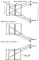
- Figure 4illustrates an autostereoscopic 3D display of the front parallax barrier type comprising an LCD 1 and an electronic parallax barrier in the form of an LCD 2.
- the LCD 1may be of the same type as shown in Figure 1 and comprises a liquid crystal layer 3 which provide a 2D array of pixels for modulating light incident from a light source (not shown) in the direction 5 with spatially multiplexed 2D images recorded from different viewpoints.
- the LCD 2is arranged and controlled so as to act as a parallax barrier providing the transmissive strips or slits such as 4.
- Each slit 4is aligned with a group of columns of pixels with each column of the group displaying a vertically extending strip of a respective 2D image.
- the LCD 2has a barrier electrode pitch which is at least twice the pixel pitch of the LCD 1.
- the structure of the LCD 2is shown in more detail in Figure 5.
- the LCD 2comprises a substrate 11 carrying an electrode arrangement and alignment layer (not shown) and a substrate 12 which carries column electrodes 13 and an alignment layer (not shown).
- a liquid crystal layer 14is disposed between the substrates 11 and 12 and comprises FLC, AFLC, or STN liquid crystal as appropriate.
- the liquid crystal layer 14comprises sharp threshold liquid crystal material and is addressed by a passive matrix electrode arrangement including the column electrodes 13.
- the electrodesare transparent and may be made of indium tin oxide (ITO). There is no black mask.
- Figure 6illustrates the appearance of a small part of the LCD 2 during operation.
- the LCD 2has orthogonally oriented input and output polarisers (not shown in Figure 5).
- column electrodes 15 and 16apply electric fields to the vertically oriented elongate pixels so as to switch the pixels to their clear or transmissive state.
- the column electrodes 15 and 16are substantially transparent but their outlines are shown in Figure 6 for the purpose of illustration.
- fringing fields or suitable electrical pulsesare applied to the electrodes so that the interelectrode gaps 17, 18 and 19 are also switched to the transmissive state.
- a vertically extending transmissive slitis therefore formed and evenly spaced parallel such slits are provided by suitably controlling the LCD 2 so as to form an electronic parallax barrier which in combination with the LCD 1 forms an autostereoscopic display.
- the electrodescause the pixels and the gaps between the pixels within the liquid crystal layer 14 to be switched to the opaque state.
- the edge portions 22may also be switched to the opaque state so that the LCD 1 acts as a parallax barrier comprising a plurality of parallel evenly spaced continuously transparent slits separated by continuously opaque regions such as 20 and 21.
- the electrode arrangement including the electrodes 13, 15 and 16supplies fields such that the whole of the liquid crystal layer 14 is switched to the clear or transmissive state.
- the LCD 2is thus continuously and substantially uniformly transmissive throughout its modulating region.
- the displayoperates as a full resolution 2D display.
- the LCD 2provides good viewing angle performance and good contrast performance without any of the visual artefacts illustrated in Figures 2 and 3.
- low levels of crosstalkare achieved in the 3D mode.
- visual artefactssuch as Moire beating with the pixel structure of the LCD 1 are greatly reduced or eliminated compared with arrangements incorporating black masks, unswitched gaps between electrodes or opaque addressing electrodes within the parallax barrier LCD.
- the parts of the liquid crystal layer 14 in the gaps between the electrodes such as 13have their own switching characteristics as illustrated in Figure 7a, which is ⁇ -V graph for pulses applied to the addressing electrodes.
- the region of the ⁇ -V plane indicated by Ais the switching region for the pixel whereas a region C is the switching region for an adjacent interelectrode gap. Both the pixel and the interelectrode gap are switched in the region B whereas neither is switched in the region D.
- the curves shown in Figure 7arelate to an arrangement having a 4 micrometre interelectrode or interpixel gap with 50 micrometre pixels.
- both horizontal and vertical gapsexist.
- the switching characteristics of the horizontal and vertical gapscan be different if they have a different orientation with respect to the rubbing or alignment direction of the liquid crystal.
- the horizontal and vertical gaps and the pixelcan be controlled as required.
- the gapsmay be switched to be entirely opaque or clear in a separate addressing phase.
- appropriate data and strobe voltagesmay be applied to the same electrodes at different times in order to control the switching of the gap and the pixel independently.
- the width of the interpixel gapsmay also be controlled so as to be appropriate for allowing switching by fringing fields of adjacent electrodes.
- the interpixel gapis preferably between 0.1 and 30 micrometres, and more preferably between 1 and 5 micrometres.
- the addressing signalsare arranged such that both the pixels and the interelectrode gaps are switched in a binary fashion. Thus, no black mask is required to achieve high contrast and low cross talk.
- the liquid crystal layer 14is controlled so that light is transmitted through all parts of the LCD 2. Thus, there is no or substantially no generation of Moire patterns.
- the LCD 1 shown in Figure 4comprises substrates 25 and 26 in addition to the pixellated liquid crystal layer 3.
- the substrates 11, 12, 25 and 26typically comprise glass of thickness 0.7 millimetres
- at least one polariser typically of 0.2 millimetres thicknessis disposed between the liquid crystal layers 3 and 14.
- the pitch of the pixels in the layer 3is typically 80 micrometres.
- the 3D displayproduces viewing zones for the eyes of the observer and the widest parts of these viewing zones are disposed in a plane parallel to the display and are referred to as viewing windows.
- viewing windows of the order of 65 millimetres corresponding to the typical interocular distanceare provided in the plane which is the nominal or best viewing distance for the display. This gives rise to a viewing distance of the order of 850 millimetres. This is relatively large for displays, for instance, of less than 12 inch diagonal size.
- the pitch of the electrodes in the LCD 2is preferably less than 40 micrometres and more preferably less than 11 micrometres.
- Figure 8illustrates a display of the type shown in Figure 4 but in which one of the middle substrates such as 26 has been eliminated.
- the displayis formed as a single device with the substrate 11 being common to the LCDs 1 and 2.
- the consequent reduction in thickness between the layers 3 and 14results in a nominal viewing distance of the order of 350 millimetres, which is more acceptable particularly for displays whose diagonal size is less than 12 inches.
- FIG. 9shows the structure of the display of Figure 8 in more detail.
- the displaycomprises an input polariser 30 for the LCD 1, an internal polariser 31 which acts as an output polariser for the LCD 1 and an input polariser for the LCD 2, and an output polariser 32 for the LCD 2.
- the polarisation absorbing directions of the polarisersare indicated by a dot for a direction normal to the plane of Figure 9 and by an arrow for a direction parallel to the plane of Figure 9.
- the LCD 1further comprises a black mask 33 which covers, for instance, semiconductor structures forming part of the LCD addressing circuitry and which is disposed on or adjacent the substrate 11 between the substrate and the internal polariser 31.
- the substrate 25carries a pixel structure defining layer, for instance in the form of a 2D array of electrodes. Examples of different configurations for defining different pixel configurations are shown at 34 and 35. Suitable colour filters (not shown) may also be provided.
- the arrangement 34comprises a conventional rectangular array of electrodes defining a corresponding array of pixels.
- the arrangement 35defines an arrangement of the type disciosed in EP 0 625 861 such that adjacent columns of pixels are horizontally substantially contiguous.
- the substrate 12carries a parallax structure defining layer 36 in the form of parallel vertically extending column electrodes. Examples of electrode arrangements are described hereinafter.
- the polarisers 30 and 31have substantially orthogonal polarising directions. Similarly, the polarisers 31 and 32 have orthogonal polarising directions. Operation of the LCD 1 will now be described for the case of the TN liquid crystal effect.
- Light from an unpolarised Lambertian light source(not shown) is linearly polarised by the input polariser 30 and passes to the liquid crystal layer 3.
- the pixels of the layer 3selectively rotate the polarisation of light passing therethrough and the internal polariser 31 analyses the output polarisation from the layer 3 in the known way for LCDs.
- Light passing through the LCD 1is thus spatially modulated with spatially multiplexed 2D images.
- the LCD 2is controlled so that transmissive slits 4 are provided and are separated by horizontally contiguous opaque regions such as 37 and 38.
- the region 4rotates the linearly polarised light from the polariser 31 by an amount which is preferably 90 degrees so that the output light passes through the output polariser 32.
- the regions 37 and 38are controlled so as not to rotate the polarisation of light from the internal polariser 31 so that the output polariser 32 blocks the light.
- the transmissive slit 4is effectively aligned with pixel columns indicated at 39, 40 and 41.
- the LCD 2thus acts as a parallax barrier and provides a number of output light cones of wedge-shape (typically two) in which light from the pixel columns 39, 40 and 41 is directed.
- This arrangementis repeated with the relative pitches of the pixel columns of the LCD 1 and the pixels of the LCD 2 being such that a viewpoint corrected display is provided and results in the viewing zones and viewing windows described hereinbefore.
- An observerwhose eyes are disposed in two adjacent viewing zones therefore sees an autostereoscopic 3D image. Each eye of the observer sees typically half of the pixels of the LCD 1 so that the individual 2D images typically have half of the spatial resolution of the LCD 1.
- the layer 36causes the whole of the liquid crystal layer 14 to be switched to a substantially uniformly transmissive state.
- the parallax barrierthus "disappears" and the LCD 2 becomes substantially invisible to an observer.
- both eyes of the observersee the whole of the LCD 1 which may therefore display 2D images at the full spatial resolution of the LCD 1.
- the absence of opaque regions such as black masks or opaque electrodes in the LCD 2substantially eliminates Moire patterns caused by beating with the structure of the LCD 1.
- the ability to produce a clear unadulterated barrier statepermits a full resolution 2D mode which is artefact free to be provided.
- the display shown in Figure 10differs from that shown in Figure 9 in that the internal polariser 31 is disposed between the substrate 11 and the liquid crystal layer 14. Such an arrangement may be favoured by fabrication requirements and operates in the same way as the display of Figure 9.
- Figure 11illustrates an arrangement in which the internal polariser 31 is omitted and the layer 14 comprises FLC incorporating a dye which is aligned with the liquid crystal in a guest-host arrangement. The absorbtion performed by the dye eliminates the need for an internal polariser.
- Light from the unpolarised sourceis polarised by the input polariser 30 and modulated by the liquid crystal layer 3.
- the pixels of the liquid crystal layer 3change the input light to proportions of wanted (W) and unwanted (UW) light polarisations.
- Wwanted
- UWunwanted
- the proportion of unwanted polarisationmust be extinguished for all barrier pixels and this is ensured by the output polariser 32.
- the proportion of wanted polarisationmust also be extinguished for the pixels of the layer 14 which are switched to the opaque state but must be transmitted by the pixels switched to the clear or transmissive state. This is achieved by the effect of the dyed FLC in the layer 14.
- the output polarisation of a standard landscape orientated panel TN active matrix LCD displayis shown typically at 45° to horizontal as shown in Figure 12.
- the polarisation of the LCD 1is aligned with the polarisation of the LCD 2 at their interface.
- the polarisers across the LCD 2are substantially orthogonal.
- the rubbing direction of the FLC alignment layeris at substantially 22.5° to the horizontal and the FLC with usual cone angle of 45° (tilt angle 22.5°) is used.
- the FLCis switchable between two stable states in which the LC molecule is aligned in the directions of the lines D1 and D2.
- one statethe LC molecules are aligned with the input polarisation so that the LC layer has no net effect and the input light is extinguished by the output polariser.
- the LC moleculesare switched to D2 and in this position the anisotropic molecule functions as a waveplate which rotates the plane of polarisation of the input light so as to allow substantial transmission of the input light through the LCD 2.
- Parallel polarisers across the LCD 2will give less contrast but higher transmission.
- FIG 13illustrates the preferred arrangement for the dyed FLC embodiments.
- the LCD 1is configured as above but in this case the LCD 2 uses an FLC which incorporates a dichroic dye, preferably a black dichroic dye in a guest-host configuration.
- the FLChas an unusually high tilt angle of 45 degrees. This is so that, in switching from D1 to D2, the FLC switches between aligned with and being orthogonal to orientations to the input polarisation state. This maximises the difference between the on and off states in this embodiment which does not require an internal polariser.
- Figure 14illustrates that other tilt angles including the standard 22.5° are possible, but in these cases the light transmission is reduced compared with that shown in Figure 13.
- the LCD 1may, for instance, be of the twisted nematic (TN) active matrix type with the black mask 33 controlling the aperture of the pixels.
- the LCD 1 for image displaymay be replaced by other types of devices, such as plasma, plasma addressed liquid crystal (PALC), Field Emission Display and electroluminescent devices.
- the display shown in Figure 15differs from that shown in Figure 10 in that the layer 34, 35 is disposed between the liquid crystal layer 3 and the substrate 11 whereas the black mask 33 is disposed between the layer 3 and the substrate 25.
- Figure 16illustrates an autostereoscopic 3D display of the micropolariser type disclosed in EP 0 721 132.
- the LCD 2differs from that, for instance, shown in Figure 15 in that it has its own input polariser 40 and output substrate 12 but omits the output polariser 32.
- a lenticular sheet 41comprising an array of parallel evenly spaced converging lenticules is disposed on the output face of the substrate 12 to form a backlight.
- the LCD 1 of Figure 16differs from that of Figure 9 in that it has no input or output polariser but has its own substrates 25 and 26.
- the LCD 2receives light 5 from an unpolarised Lambertian light source 5 which is polarised by the input polariser 40.
- the contiguous backlight pixel structure defining layer 36forms a plurality of contiguous pixels within the liquid crystal layer 14 which are elongate, vertical and parallel with alternate pixels supplying output light of orthogonal linear polarisations.
- the lenticular sheet 41generates the viewing zones by directing light from the layer 14 into contiguous light cones or wedges which are modulated by the pixels of the LCD 1.
- the display shown in Figure 16may be used to track movement of an observer so that the viewing zones or windows are maintained at the eyes of the observer, who may therefore perceive a 3D image throughout an enlarged viewing region compared with untracked displays.
- the pixels of the LCD 2are controlled in response to the position of the observer as detected by an observer tracking system.
- the adjacent orthogonally polarising pixelsare effectively moved so that the viewing windows track movements of the observer.
- the pixels of the LCD 2are controlled so as to provide light of uniform polarisation across the LCD 2.
- the observermay therefore view a 2D image with the full spatial resolution of the LCD 1.
- FIG 17differs from that shown in Figure 4 in that the optical order of the LCD 1 and the LCD 2 is reversed. This arrangement therefore acts as a rear parallax barrier 3D autostereoscopic display but otherwise operates in the same way as the display of Figure 4.
- Figure 18illustrates a display which differs from that of Figure 8 in that it is a rear parallax barrier display.
- Figure 19illustrates the structure of the display of Figure 18, which structure differs from that of Figure 9 in the order of components. Operation is as described with respect to Figure 9.
- the display shown in Figure 20differs from that shown in Figure 19 in that the internal polariser 31 is disposed on the other side of the substrate 12.
- Figure 21illustrates a display which differs from that shown in Figure 19 in that the internal polariser 31 is omitted and the liquid crystal layer 14 contains a dye in a guest-host arrangement. Operation of the display shown in Figure 21 is the same as that shown in Figure 11.
- Figure 22shows a display which differs from that shown in Figure 20 in that the positions of the layer 34, 35 and the black mask 33 are interchanged.
- Figure 23shows a display which differs from that shown in Figure 21 in that the layer 14 comprises a liquid crystal layer switchable reflector.
- the layer 14comprises a liquid crystal layer switchable reflector.
- FIGS 24, 25 and 26illustrate embodiments in which the LCD 2 is implemented with a reflective as opposed to an absorptive barrier. This can improve the overall light efficiency of the rear parallax element embodiments.
- the input lightis converted to linear polarisation by the polariser 30, then to circular polarisation by a wideband quarter waveplate 50.
- the LCD 2has a layer 51 comprising a chirped pitch cholesteric switchable reflector.
- the layerIn the barrier mode, the layer has regions of cholesteric reflector and clear (non-cholesteric) states. Switching between these states is accomplished as described hereinbefore. Circular polarisation light impinging on the cholesteric reflector is reflected whereas that impinging on the clear parts is transmitted.
- the transmitted lightis then converted to linear polarisation by a quarter waveplate 52 so as to match the required input polarisation state of the subsequent LCD 1.
- the cholesteric statehas a chirped pitch in order to reflect circular polarisation over both a wide angle and a wide range of wavelengths.
- Figure 25differs from that of Figure 24 by an alternative position for the linear polariser.
- a layer 51a which contains a wide band diffractive reflectoris used as the parallax generating element.
- the sheet reflectoris enabled/disabled in regions required to be transmissive (so as to form a parallax SLM) by controlling the orientation of adjacent anisotropic LC molecules by an electric field in the manner described hereinbefore.
- the gratingis disabled by switching the adjacent LC layer so that there is substantially no refractive index difference between the oriented adjacent LC and the diffractive reflector. This effectively washes out the grating which in these regions becomes invisible.
- the adjacent LCis switched to an orientation in which there is a refractive index difference between the grating and the LC, thereby enabling the reflective function of the grating.
- Figure 27aillustrates an electrode arrangement for the LCD 2 of Figure 5.
- a continuous plane counter electrode 60is disposed on the substrate 11 whereas the parallax structure defining layer 36 has the form of an electrode having formed therein a plurality of slits for corresponding to the parallax barrier slits.
- the arrangementpermits switching between the clear mode and the barrier mode in which the positions of the slits are fixed.
- the LCDmay be switched from one state to another by applying a suitable signal (V on/off).
- Figure 27billustrates an electrode arrangement for the LCD 2 having regions of shared electrodes which permits 2D/3D operation in a number of configurable zones.
- SLMsare suitable for use with mechanical tracking, for instance as disclosed in British Patent Application No. 9619097.0.
- the electrode arrangement shown in Figure 28comprises a continuous plane electrode 60 facing a plurality of parallel uniformly spaced column electrodes such as 61.
- the pixels and interelectrode gapsmay be switched individually by supplying suitable signals V1, V2, ... Vn to the individual electrodes which allows the slit locations of the barrier in the 3D mode to be moved so as to perform electronic tracking, for instance as described hereinafter.
- full resolution 2D zoneswhich extend the full height of the display may be combined with 3D zones by suitably controlling the signals supplied to the electrodes 61.
- Figure 29illustrates an XY passive matrix addressing arrangement comprising column electrodes such as 61 and row electrodes such 62.
- Strobe signals Vr1, Vr2, ... Vrnmay be applied in sequence to the electrodes 62 so as to enter data in accordance with the column signals V1, ... Vn a row at a time so as to refresh the mode of the display.
- the gaps between pixelsmay be controlled by fringing fields or by "frame ahead gap blanking". Alternatively, the gaps may be switched by different strobe and data voltages applied to the same row and column electrodes and optionally to other row and column electrodes without altering the state of the adjacent pixels.
- FIG. 29may be used to provide any desired configuration of 2D and 3D image zones simultaneously.
- Figure 30illustrates a 3D background 63 having 2D image zones 64, 65 and 66.
- the 2D zone 66has an inset 3D image zone 67.
- the corresponding pixels of the LCD 2are controlled to provide parallax barriers whereas the pixels in the regions of the 2D zones are controlled to be transmissive.
- the presence of the parallax barrier over the 3D regionsgives a difference in intensity between the 2D and 3D zones which may be compensated for electronically in the drive signal. Compensation by setting the 2D zones to an intermediate attenuating grey level may be used to achieve the same effect but is not appropriate for the LCD 2 when using binary switching effects, for instance in the case of standard FLCs.
- the presence of a border around an inset 2D or 3D image zoneprevents vertical parallax caused by the separation of the LCDs 1 and 2 seen by a viewer above or below the axis of the display from making the edge pixels of an inset zone appear in the wrong image zone.
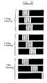
- Figure 31shows a temporally multiplexed 3D autostereoscopic display in which the image LCD is a fast SLM, for instance of the FLC type, and the parallax barrier LCD is likewise of the fast switching type such as FLC.
- the middle part of Figure 31illustrates the generation of a left eye viewing window 70 during a first field in which image data of a first 2D image are displayed by the LCD 1.
- the windowsare produced in a plurality of lobes as is known in 3D display technology.
- the slits 4 of the parallax barrier formed by the LCD 2are located in a first lateral position with respect to the pixels of the LCD 1.
- FIG. 31illustrates generation of right eye viewing windows 71.
- a second field of image data representing an image to be viewed by the right eye of the observeris displayed by the LCD 1.
- the LCD 2is controlled so that the pixels 4 have a different lateral position with respect to the pixels of the LCD 1.
- Figure 32illustrates a temporally multiplexed display which differs from that shown in Figure 31 in that the optical order of the fast SLM 1 and the dynamic parallax barrier LCD 2 are reversed.
- Figure 33illustrates use of the steerable backlight shown in Figure 16 in a temporally multiplexed display.
- 2D image dataare supplied in sequence to the fast SLM 1 and the LCD 2 is controlled such that light corresponding to each 2D image is directed to a respective one of the viewing windows 70 and 71.
- Figure 34illustrates an arrangement combining spatial and temporal multiplexing to provide four viewing windows 72 to 75.
- two spatially multiplexed 2D imagesare displayed by the SLM 1.
- two viewing windows 73 and 75are provided in one field whereas two viewing windows 72 and 74 are provided in the next field.
- the display of Figure 35differs from that shown in Figure 34 in that the optical order of the SLM 1 and the barrier 2 is reversed.
- Figure 36illustrates a display of the type shown in Figure 9 for providing a pair of viewing windows for a first observer and another pair of viewing windows for a second observer. The creation of the individual viewing windows is shown in the middle and lower parts of Figure 36.
- the slits in the two fields of the displays shown in Figures 32 and 35need not be contiguous with each other. Further, the width of the slits can be electrically adjusted to control brightness against viewing window quality, which is a measure of 3D crosstalk level.
- Figure 38illustrates this for a pixel aperture 76 of rectangular shape and for a narrow slit 77 and a wide slit 78.
- the variation of intensity with observer position for the slits 77 and 78is illustrated at 79 and 80, respectively.
- the profile 79shows that the intensity of light is reduced but the window shape is better.
- the corresponding intensity profile 80shows greater intensity but a worse window shape.
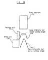
- FIG 37illustrates different tracking modes for an LCD 2 of the type shown in Figure 5.
- Each slitis made up of a number of pixels and will be illustrated for the case of four pixels.
- the four pixelsare controlled so as to be transparent.
- the pixelsmay be switched such that one pixel at one edge of the slit is switched to black as one pixel next to the other edge of the slit is switched to white. This provides one step tracking and minimises flicker.
- Optical performanceis optimum for one step tracking in that undesirable visible artefacts are minimised and this therefore represents the normal operation.
- the middle part of Figure 37illustrates two step tracking in which two pixels at one edge are switched to black as two pixels adjacent the other edge are switched to white. This mode of tracking allows for higher speed observer movements to be accommodated.
- Figure 37illustrates jump tracking in which no pixels remain clear i.e. the location of the transmissive slit jumps so that there is no overlap between one slit position and the next slit position. This mode allows for extreme observer movement and for error recovery.
Landscapes
- Engineering & Computer Science (AREA)
- Multimedia (AREA)
- Signal Processing (AREA)
- Physics & Mathematics (AREA)
- General Physics & Mathematics (AREA)
- Optics & Photonics (AREA)
- Liquid Crystal (AREA)
- Devices For Indicating Variable Information By Combining Individual Elements (AREA)
- Transforming Electric Information Into Light Information (AREA)
- Testing, Inspecting, Measuring Of Stereoscopic Televisions And Televisions (AREA)
Description
- The present invention relates to a spatial light modulator. The presentinvention also relates to a directional display such as an autostereoscopicdisplay. The invention further relates to a directional light source, forinstance for use in directional displays.
- A known type of autostereoscopic three dimensional (3D) display isshown in Figure 1 of the accompanying drawings. The display comprisesa spatial light modulator in the form of a liquid crystal device (LCD) 1associated with a parallax element in the form of a
parallax barrier 2. TheLCD 1 comprises a plurality of picture elements (pixels) arranged as a twodimensional (2D) array. The pixels are formed in aliquid crystal layer 3and are configured as groups of columns of pixels. Each group isassociated with a verticallyoriented slit 4 of theparallax barrier 2. Thegroups of columns may comprise two or more columns and each columnis arranged to display a vertical slice of a respective 2D image. Thedisplay is illuminated by a suitable backlight (not shown) in the directionofarrow 5 and theparallax barrier slits 4 produce cones of light, in theform of wedges, corresponding to the columns of each group. Inviewpoint corrected displays, these light wedges overlap to define left andright viewing zones for the left and right eyes, respectively, of an observer.Thus, provided the eyes of the observer remain in the correct viewingzones, the observer can perceive a 3D image. - In order to provide greater viewing freedom for the observer, it is knownto provide an observer tracking display in which the viewing zones move so as to track the observer within a permissible range of movement. In thetype of display shown in Figure 1, this may be achieved by means of amechanical tracking system. Such a system measures the position of theobserver and moves the
parallax barrier 2 laterally with respect to theLCD 1 so that the eyes of the observer remain within the correct viewing zones.However, such arrangements require movement of optical componentsand this increases weight and power consumption of the display whilereducing its ruggedness. For a display which provides two viewing zones,each eye of the observer sees a maximum of half the number of pixels oftheLCD 1, both in the 3D mode and in a 2D mode of the display whereboth eyes see the same image information. Therefore, in the 2D mode,half of the LCD resolution is effectively wasted. - It is also possible to provide an observer tracking autostereoscopic 3Ddisplay without moving parts, for instance as disclosed in
EP 0 721 131andEP 0 726 482. However, such displays allow each eye of theobserver to see only one third of the pixels of the LCD in both 3D and 2Dmodes of operation. - A
conventional parallax barrier 2 essentially comprises an opaque plate orlayer having light-transmissive slits 4 formed parallel to each other andevenly spaced. The slits extend vertically for providing lateral parallax.However, thepassive parallax barrier 2 may be replaced by an activeparallax barrier, for instance as disclosed in JP 03-119889. The activebarrier comprises a twisted nematic (TN) LCD having vertically stripedelectrodes and interelectrode gaps. The electrodes define the pixels of theLCD whereas the interelectrode gaps define gaps between the pixels which remain substantially unswitched irrespective of the electric fieldsapplied to the TN liquid crystal by the electrodes. The pitches of thebarrier and display SLMs are substantially equal. - The LCD may be configured to provide normally white or normally blackoperation. Figure 2 illustrates the magnified appearance of a small part ofan LCD operated in the normally white mode. In particular, the LCD isarranged to act as a parallax barrier in that the vertically extending
pixel 6is controlled to be transparent so as to constitute a slit of the barrierwhereas the pixels between the transmissive slits, such as 8, are controlledto be opaque. However, the unswitched regions 9 remain partially orwholly transmissive. This prevents good contrast being achieved in whatshould be the opaque regions of the barrier and can result in crosstalkleading to undesirable visible artefacts in the 3D image seen by theobserver. In order to display a 2D image, the whole of theparallax barrier 2 can be made substantially uniformly transmissive so that all of the pixelsof the LCD are visible to both eyes of the observer and the full spatialresolution of the LCD can be used in such a 2D mode. In this mode, theparallax barrier is effectively "switched out" unlike in the 2D mode ofdisplays having non-switchable parallax barriers. - Figure 3 illustrates the appearance of the
active barrier 2 when configuredto operate in the normally black mode. Operation in either the normallyblack mode or the normally white mode is fixed at the time ofmanufacture. Again, thepixel 6 is controlled to be transmissive so as toform a slit and the slits are separated by opaque regions. However, thevertical gap 10 between thepixels active barrier 2 and theunderlying structure of theLCD 1. Further, there is increased diffractionfrom thebarrier 2. - A known display disclosed in a Sanyo press release entitled "2D/3DSwitchable Display" issued on 10th May, 1996 discloses a display whichcan be switched between 2D and 3D modes in each of sixteen fixedzones. This is achieved by the use of a passive rear parallax barrier and anoverlaid 4x4 segment electrically switchable diffuser in the form of apolymer dispersed liquid crystal.
- A projection display in which the interelectrode gaps throughout thedisplay are switched black ahead of operating time is disclosed inMcDonnell 93. This is done to avoid using a separate black matrix layer.
EP 0 540 137 discloses a 3D image display which has an electricallygenerated parallax barrier formed in an LCD. However, there is nosubstantial disclosure of the structure or operation of such a parallax barrier. In particular, there is no disclosure in relation to controlling theliquid crystal in the gaps betwen electrodes.- US 5 122 888 discloses a camera focusing plate containing a dynamicliquid crystal. A phased diffraction grating can be established in theliquid crystal by applying an electric field so as to rotate the molecules ofthe liquid crystal and change the refractive index to light passing throughthe liquid crystal in order to produce a diffuser. There is disclosure ofrefractive index change at the gaps between electrodes by a leakageelectric field but the resulting refractive index change is less than thatwhich occurs in the liquid crystal at the electrodes and a sinewaverefractive index profile is created.
EP 0 586 098 discloses a light modulating apparatus for use inreconstruction of a one-dimensional hologram. The apparatus contains anumber of pixels which ahve a small width in the horizontal direction butwhich are relatively tall. Driving elements for the pixels are provided atthe ends of the pixels and are not placed between adjacent pixels. Theapparatus is said to have a good resolution in the horizontal direction.However, there is no disclosure relating to switching of a display mediumat gaps between electrodes.- According to a first aspect of the invention, there is provided a spatial lightmodulatoras defined in
claim 1. The spatial light modulator comprises a modulator region which is switchablebetween a clear mode, in which the region is of substantially uniformtransmissivity, and a barrier mode, in which the region has a plurality of evenly spaced parallel transmissive strips extending in a first direction and separated bycontinuous substantially opaque sub-regions, the region comprising picture elementsdefined by addressing electrodes separated by gaps, the modulator comprising meansfor switching the transmissivity of the gaps between the electrodes by fringing fields. - The picture elements may comprise elongate picture elements defined by respectiveelongate addressing electrodes extending in the first direction. The picture elementsmay be switchable together to opaque to define the sub-regions and may be spaced apartto define the transmissive slits. The gaps may be switchable by the means betweentransmissive and opaque independently of the picture elements.
- The picture elements may comprise a two-dimensional array of picture elements, eachof which is independently switchable between transmissive and opaque. The gaps maybe independently switchable between transmissive and opaque.
- The modulator may comprise a liquid crystal device including a first layer of liquidcrystal material. The first layer may comprise ferroelectric liquid crystal material, anti-ferroelectricliquid crystal material or super-twisted nematic liquid crystal material. Thefirst layer may include an anisotropic dye.
- The addressing electrodes may comprise a passive matrix addressing arrangement.
- The opaque sub-regions may be reflective.
- According to a second aspect of the invention, there is provided a spatial lightmodulator as defined in
claim 14. The spatial light modulator comprises a modulator region which is switchable between a firstmode, in which the region is arranged to supply light of a substantially uniform firstpolarisation, and a second mode, in which the region is arranged to supply light of thefirst polarisation in a plurality of evenly spaced parallel strips and to supply light of asecond polarisation, different from the first polarisation, in continuous sub-regionswhich separate the strips, the region comprising picture elements defined by addressingelectrodes separated by gaps, the modulator comprising means for switching thetransmissivity of the gaps between the electrodes by fringing fields. - The second polarisation may be orthogonal to the first polarisation.
- According to a third aspect of the invention, there is provided a directional displaycomprising the modulator in accordance with the first or second aspects of theinvention co-operating with an image display.
- The image display may comprise a further spatial light modulator. The further spatiallight modulator may comprise a further liquid crystal device including a second layer ofliquid crystal material. The display may comprise first and second substrates with thefirst layer therebetween and a third substrate with the second layer between the secondand third substrates. The display may comprise a single polariser between the first andsecond layers.
- According to a fourth aspect of the invention, there is provided a directional light sourcecomprising a modulator according to the first or second aspects of the inventionco-operating with a diffuse light source. The light source may comprise a lenticular sheet having lenticulesextending in the first direction.
- It is thus possible to provide an SLM which is suitable for use inautostereoscopic and stereoscopic 3D displays. For instance, in anautostereoscopic display, the SLM may be operated in the barrier mode todefine a parallax barrier having good contrast performance and providinglow levels of crosstalk. In the clear mode, substantially uniformtransmissivity is provided so that the full resolution of an associated imagedisplay may be used while Moire effects with the display structure aresubstantially reduced or eliminated. In some embodiments, different areasof the SLM may be operated simultaneously in the clear and barrier modesso that one or more parts of a directional display displays a 3D image andone or more other parts display a 2D image. Also, in some embodiments,the barrier mode is such that the positions of the transmissive slits can beelectronically varied perpendicularly to the first direction. Such anarrangement permits observer tracking with no moving parts in anautostereoscopic 3D display. For such an application, the SLM may bedisposed adjacent the image display so as to control the positions ofviewing zones. In an alternative arrangement, the SLM may be associatedwith a backlight to provide a directional light source emitting light in lightbeams or "wedges" whose direction can be controlled electronically.
- The SLM does not have a black mask so that the manufacturing process issimplified. Full brightness is achieved in parts of the SLM which arecontrolled to be transmissive or "white" and the whole of the modulator region or user-selected parts thereof can be switched so as to be whollyclear or "white" without leaving residual black mask areas which wouldgenerate Moire patterns by beating with the similar pixel structure of animage display.
- It is possible to make use of "bistable"liquid crystal materials such asferroelectric liquid crystals (FLC), anti-ferroelectric liquid crystals (AFLC)with a sharply defined electro-optic transition, and super-twisted nematic(STN) liquid crystals. This permits the use of passive matrix addressing sothat there are no interelectrode opaque regions as in the case of activematrix addressing where electronic devices such as thin film transistorshave to be located in the gaps between opaque addressing electrodes.Power consumption is also reduced so that the SLM is suitable for use inbattery powered displays such as lap top personal computers (PC) andpersonal digital assistants (PDA). Such an SLM therefore has advantages ofimproved aperture and hence brightness, simplicity and reduced costcompared with twisted nematic (TN) techniques using thin film transistors,for instance as disclosed in
JP 0 3-119889, in addition to other advantagesmentioned hereinbefore. - The invention will be further described, by way of example, withreference to the accompanying drawings, in which:
- Figure 1 shows a horizontal cross section of a known type ofautostereoscopic 3D display;
- Figure 2 illustrates the appearance of a representative subregion of an SLMoperating in the normally white mode to provide an electronic parallaxbarrier;
- Figure 3 illustrates the appearance of an SLM operating in the normallyblack mode to provide an electronic parallax barrier;
- Figure 4 shows a horizontal cross-section of part of an autostereoscopic3D display constituting an embodiment of the invention;
- Figure 5 shows a horizontal cross section of an SLM constituting anembodiment of the invention;
- Figure 6 illustrates the appearance of the SLM of Figure 5 around oneaperture during operation;
- Figure 7a is a graph of pulse length in microseconds against pulseamplitude in volts showing τ-V curves for pixel and interpixel liquidcrystal regions;
- Figure 7b is a graph of transmittance against voltage illustrating pixel andinterpixel switching;
- Figure 8 shows a horizontal cross section of a 3D display constituting anembodiment of the invention;
- Figure 9 illustrates in more detail the structure of the display shown inFigure 8;
- Figure 10 is a view similar to Figure 9 showing an alternative position ofan internal polariser;
- Figure 11 is a view similar to Figure 9 in which an internal polariser isreplaced by dye in a guest-host arrangement;
- Figure 12 illustrates a suitable orientation of the rubbing direction of theFLC barrier SLM with respect to the display SLM;
- Figure 13 illustrates a preferred tilt angle for a dyed FLC;
- Figure 14 illustrates a standard tilt angle for a dyed FLC;
- Figure 15 shows the display of Figure 10 with a black mask in analternative position;
- Figure 16 shows the structure of a 3D display using a directional backlightconstituting an embodiment of the invention;
- Figures 17 to 22 correspond to Figures 4, 8 to 11 and 15, respectively, butshow alternative configurations of 3D displays having rear parallaxbarriers;
- Figure 23 shows the structure of a 3D display having a rear reflectiveparallax barrier;
- Figures 24 to 26 illustrate alternative arrangements of reflective parallaxbarriers in an SLM;
- Figure 27a illustrates an electrode pattern for an SLM which is switchablebetween a barrier state providing fixed transmissive slits and a clear state;
- Figure 27b illustrates an electrode pattern for an SLM which is switchablein regions;
- Figure 28 illustrates an electrode pattern for an SLM which, in its barriermode, provides slits whose positions are controllable so as to permitobserver tracking in a 3D display;
- Figure 29 illustrates an electrode pattern for an SLM permitting observertracking and dynamically configurable 2D and 3D zones in a 3D display;
- Figure 30 illustrates a possible configuration of 2D and 3D zones on adisplay having the electrode pattern of Figure 29;
- Figures 31 and 32 illustrate two arrangements of temporally multiplexed3D displays using an SLM of the type illustrated in Figures 8 and 18;
- Figure 33 illustrates use of an SLM of the type shown in Figure 5 toprovide a steerable backlight in a temporally multiplexed 3D display;
- Figure 34 illustrates use of an SLM of the type shown in Figure 5 in a 3Ddisplay having spatial and temporal multiplexing;
- Figure 35 illustrates a display similar to Figure 34 but with a rear parallaxbarrier;
- Figure 36 illustrates operation of a display of the type shown in Figure 8for simultaneously tracking two observers;
- Figure 37 illustrates the appearance of an SLM of the type shown in Figure5 for different observer tracking modes; and
- Figure 38 is a diagram illustrating the effect of slit width on windowquality or crosstalk and brightness.
- Like reference numerals refer to like parts throughout the drawings.
- Figure 4 illustrates an autostereoscopic 3D display of the front parallaxbarrier type comprising an
LCD 1 and an electronic parallax barrier in theform of anLCD 2. TheLCD 1 may be of the same type as shown in Figure1 and comprises aliquid crystal layer 3 which provide a 2D array of pixelsfor modulating light incident from a light source (not shown) in thedirection 5 with spatially multiplexed 2D images recorded from differentviewpoints. - The
LCD 2 is arranged and controlled so as to act as a parallax barrierproviding the transmissive strips or slits such as 4. Eachslit 4 is alignedwith a group of columns of pixels with each column of the groupdisplaying a vertically extending strip of a respective 2D image. Asdescribed hereinafter, theLCD 2 has a barrier electrode pitch which is atleast twice the pixel pitch of theLCD 1. - The structure of the
LCD 2 is shown in more detail in Figure 5. TheLCD 2 comprises asubstrate 11 carrying an electrode arrangement andalignment layer (not shown) and asubstrate 12 which carriescolumnelectrodes 13 and an alignment layer (not shown). Aliquid crystal layer 14 is disposed between thesubstrates liquid crystallayer 14 comprises sharp threshold liquid crystal material and is addressedby a passive matrix electrode arrangement including thecolumnelectrodes 13. The electrodes are transparent and may be made of indiumtin oxide (ITO). There is no black mask. - Figure 6 illustrates the appearance of a small part of the
LCD 2 duringoperation. TheLCD 2 has orthogonally oriented input and outputpolarisers (not shown in Figure 5). In a barrier mode of operation,columnelectrodes column electrodes interelectrode gaps LCD 2 so as to form an electronic parallax barrierwhich in combination with theLCD 1 forms an autostereoscopic display. - In the regions such as 20 and 21, the electrodes cause the pixels and thegaps between the pixels within the
liquid crystal layer 14 to be switchedto the opaque state. Theedge portions 22 may also be switched to theopaque state so that theLCD 1 acts as a parallax barrier comprising aplurality of parallel evenly spaced continuously transparent slits separatedby continuously opaque regions such as 20 and 21. - In the clear mode of operation, the electrode arrangement including the
electrodes liquidcrystal layer 14 is switched to the clear or transmissive state. TheLCD 2 isthus continuously and substantially uniformly transmissive throughout itsmodulating region. In this clear mode of theLCD 2, the display operatesas a full resolution 2D display. - The
LCD 2 provides good viewing angle performance and good contrastperformance without any of the visual artefacts illustrated in Figures 2 and3. Thus, when used in the autostereoscopic 3D display shown in Figure 4,low levels of crosstalk are achieved in the 3D mode. In the 2D mode,visual artefacts such as Moire beating with the pixel structure of theLCD 1are greatly reduced or eliminated compared with arrangementsincorporating black masks, unswitched gaps between electrodes oropaque addressing electrodes within the parallax barrier LCD. - The parts of the
liquid crystal layer 14 in the gaps between the electrodessuch as 13 have their own switching characteristics as illustrated in Figure7a, which is τ-V graph for pulses applied to the addressing electrodes. Theregion of the τ-V plane indicated by A is the switching region for the pixelwhereas a region C is the switching region for an adjacent interelectrodegap. Both the pixel and the interelectrode gap are switched in the regionB whereas neither is switched in the region D. - The curves shown in Figure 7a relate to an arrangement having a 4micrometre interelectrode or interpixel gap with 50 micrometre pixels.
- In the case of 2D matrix electronic parallax barriers, both horizontal andvertical gaps exist. The switching characteristics of the horizontal andvertical gaps can be different if they have a different orientation withrespect to the rubbing or alignment direction of the liquid crystal. Thus,the horizontal and vertical gaps and the pixel can be controlled asrequired.
- The gaps may be switched to be entirely opaque or clear in a separateaddressing phase. Alternatively, appropriate data and strobe voltages maybe applied to the same electrodes at different times in order to control theswitching of the gap and the pixel independently. The width of theinterpixel gaps may also be controlled so as to be appropriate for allowingswitching by fringing fields of adjacent electrodes. For this purpose, theinterpixel gap is preferably between 0.1 and 30 micrometres, and morepreferably between 1 and 5 micrometres. The addressing signals are arranged such that both the pixels and the interelectrode gaps areswitched in a binary fashion. Thus, no black mask is required to achievehigh contrast and low cross talk. In the full resolution 2D mode, the
liquidcrystal layer 14 is controlled so that light is transmitted through all parts oftheLCD 2. Thus, there is no or substantially no generation of Moirepatterns. - The
LCD 1 shown in Figure 4 comprisessubstrates liquid crystal layer 3. Thesubstrates liquid crystal layers layer 3 is typically 80 micrometres. As describedhereinbefore, the 3D display produces viewing zones for the eyes of theobserver and the widest parts of these viewing zones are disposed in aplane parallel to the display and are referred to as viewing windows.Typically, viewing windows of the order of 65 millimetres correspondingto the typical interocular distance are provided in the plane which is thenominal or best viewing distance for the display. This gives rise to aviewing distance of the order of 850 millimetres. This is relatively largefor displays, for instance, of less than 12 inch diagonal size. - In this example, the pitch of the electrodes in the
LCD 2 is preferably lessthan 40 micrometres and more preferably less than 11 micrometres. - Figure 8 illustrates a display of the type shown in Figure 4 but in whichone of the middle substrates such as 26 has been eliminated. The displayis formed as a single device with the
substrate 11 being common to theLCDs layers - Figure 9 shows the structure of the display of Figure 8 in more detail. Thedisplay comprises an
input polariser 30 for theLCD 1, aninternal polariser 31 which acts as an output polariser for theLCD 1 and an input polariserfor theLCD 2, and anoutput polariser 32 for theLCD 2. The polarisationabsorbing directions of the polarisers are indicated by a dot for a directionnormal to the plane of Figure 9 and by an arrow for a direction parallel tothe plane of Figure 9. - The
LCD 1 further comprises ablack mask 33 which covers, for instance,semiconductor structures forming part of the LCD addressing circuitry andwhich is disposed on or adjacent thesubstrate 11 between the substrateand theinternal polariser 31. Thesubstrate 25 carries a pixel structuredefining layer, for instance in the form of a 2D array of electrodes.Examples of different configurations for defining different pixelconfigurations are shown at 34 and 35. Suitable colour filters (not shown)may also be provided. Thearrangement 34 comprises a conventionalrectangular array of electrodes defining a corresponding array of pixels.Thearrangement 35 defines an arrangement of the type disciosed inEP 0 625 861 such that adjacent columns of pixels are horizontally substantiallycontiguous. - The
substrate 12 carries a parallaxstructure defining layer 36 in the formof parallel vertically extending column electrodes. Examples of electrodearrangements are described hereinafter. - The
polarisers polarisers LCD 1 will now be described for the case ofthe TN liquid crystal effect. Light from an unpolarised Lambertian lightsource (not shown) is linearly polarised by theinput polariser 30 andpasses to theliquid crystal layer 3. The pixels of thelayer 3 selectivelyrotate the polarisation of light passing therethrough and theinternalpolariser 31 analyses the output polarisation from thelayer 3 in the knownway for LCDs. Light passing through theLCD 1 is thus spatiallymodulated with spatially multiplexed 2D images. - In the autostereoscopic 3D mode, the
LCD 2 is controlled so thattransmissive slits 4 are provided and are separated by horizontallycontiguous opaque regions such as 37 and 38. In particular, theregion 4rotates the linearly polarised light from thepolariser 31 by an amountwhich is preferably 90 degrees so that the output light passes through theoutput polariser 32. Theregions internal polariser 31 so that theoutput polariser 32 blocks the light. - The
transmissive slit 4 is effectively aligned with pixel columns indicatedat 39, 40 and 41. TheLCD 2 thus acts as a parallax barrier and provides anumber of output light cones of wedge-shape (typically two) in which lightfrom thepixel columns LCD 1 andthe pixels of theLCD 2 being such that a viewpoint corrected display isprovided and results in the viewing zones and viewing windows describedhereinbefore. An observer whose eyes are disposed in two adjacentviewing zones therefore sees an autostereoscopic 3D image. Each eye ofthe observer sees typically half of the pixels of theLCD 1 so that theindividual 2D images typically have half of the spatial resolution of theLCD 1. - In the 2D mode, the
layer 36 causes the whole of theliquid crystal layer 14 to be switched to a substantially uniformly transmissive state. Theparallax barrier thus "disappears" and theLCD 2 becomes substantiallyinvisible to an observer. Thus, both eyes of the observer see the whole oftheLCD 1 which may therefore display 2D images at the full spatialresolution of theLCD 1. The absence of opaque regions such as blackmasks or opaque electrodes in theLCD 2 substantially eliminates Moirepatterns caused by beating with the structure of theLCD 1. The ability toproduce a clear unadulterated barrier state permits a full resolution 2Dmode which is artefact free to be provided. - The display shown in Figure 10 differs from that shown in Figure 9 in thatthe
internal polariser 31 is disposed between thesubstrate 11 and theliquid crystal layer 14. Such an arrangement may be favoured by fabrication requirements and operates in the same way as the display ofFigure 9. - Figure 11 illustrates an arrangement in which the
internal polariser 31 isomitted and thelayer 14 comprises FLC incorporating a dye which isaligned with the liquid crystal in a guest-host arrangement. The absorbtionperformed by the dye eliminates the need for an internal polariser. - Light from the unpolarised source is polarised by the
input polariser 30and modulated by theliquid crystal layer 3. Depending on the requiredgrey scale level, the pixels of theliquid crystal layer 3 change the inputlight to proportions of wanted (W) and unwanted (UW) light polarisations.In order for the grey scale content to be visible, the proportion ofunwanted polarisation must be extinguished for all barrier pixels and thisis ensured by theoutput polariser 32. The proportion of wantedpolarisation must also be extinguished for the pixels of thelayer 14 whichare switched to the opaque state but must be transmitted by the pixelsswitched to the clear or transmissive state. This is achieved by the effectof the dyed FLC in thelayer 14. - The output polarisation of a standard landscape orientated panel TN activematrix LCD display is shown typically at 45° to horizontal as shown inFigure 12. To make the best use of this light without unnecessary losses, itis preferable to configure the
LCD 2 using the FLC effect as illustrated inthe bottom half of Figure 11. The polarisation of theLCD 1 is aligned withthe polarisation of theLCD 2 at their interface. The polarisers across theLCD 2 are substantially orthogonal. In this case, as illustrated, the rubbing direction of the FLC alignment layer is at substantially 22.5° to thehorizontal and the FLC with usual cone angle of 45° (tilt angle 22.5°) isused. In this mode, the FLC is switchable between two stable states inwhich the LC molecule is aligned in the directions of the lines D1 and D2.In one state (off), the LC molecules are aligned with the input polarisationso that the LC layer has no net effect and the input light is extinguished bythe output polariser. In the other state (on), the LC molecules are switchedto D2 and in this position the anisotropic molecule functions as awaveplate which rotates the plane of polarisation of the input light so as toallow substantial transmission of the input light through theLCD 2.Parallel polarisers across theLCD 2 will give less contrast but highertransmission. - Figure 13 illustrates the preferred arrangement for the dyed FLCembodiments. The
LCD 1 is configured as above but in this case theLCD 2 uses an FLC which incorporates a dichroic dye, preferably a blackdichroic dye in a guest-host configuration. In this case the FLC has anunusually high tilt angle of 45 degrees. This is so that, in switching fromD1 to D2, the FLC switches between aligned with and being orthogonal toorientations to the input polarisation state. This maximises the differencebetween the on and off states in this embodiment which does not requirean internal polariser. - Figure 14 illustrates that other tilt angles including the standard 22.5° arepossible, but in these cases the light transmission is reduced comparedwith that shown in Figure 13.
- The
LCD 1 may, for instance, be of the twisted nematic (TN) active matrixtype with theblack mask 33 controlling the aperture of the pixels.TheLCD 1 for image display may be replaced by other types of devices,such as plasma, plasma addressed liquid crystal (PALC), Field EmissionDisplay and electroluminescent devices. - The display shown in Figure 15 differs from that shown in Figure 10 inthat the
layer liquid crystal layer 3 and thesubstrate 11 whereas theblack mask 33 is disposed between thelayer 3and thesubstrate 25. - Figure 16 illustrates an autostereoscopic 3D display of the micropolarisertype disclosed in
EP 0 721 132. TheLCD 2 differs from that, for instance,shown in Figure 15 in that it has itsown input polariser 40 andoutputsubstrate 12 but omits theoutput polariser 32. Alenticular sheet 41comprising an array of parallel evenly spaced converging lenticules isdisposed on the output face of thesubstrate 12 to form a backlight. TheLCD 1 of Figure 16 differs from that of Figure 9 in that it has no input oroutput polariser but has itsown substrates - The
LCD 2 receives light 5 from an unpolarised Lambertianlight source 5which is polarised by theinput polariser 40. In the 3D mode of operation,the contiguous backlight pixelstructure defining layer 36 forms a pluralityof contiguous pixels within theliquid crystal layer 14 which are elongate,vertical and parallel with alternate pixels supplying output light oforthogonal linear polarisations. Thelenticular sheet 41 generates the viewing zones by directing light from thelayer 14 into contiguous lightcones or wedges which are modulated by the pixels of theLCD 1. - The display shown in Figure 16 may be used to track movement of anobserver so that the viewing zones or windows are maintained at the eyesof the observer, who may therefore perceive a 3D image throughout anenlarged viewing region compared with untracked displays. The pixels ofthe
LCD 2 are controlled in response to the position of the observer asdetected by an observer tracking system. The adjacent orthogonallypolarising pixels are effectively moved so that the viewing windows trackmovements of the observer. - In the 2D mode, the pixels of the
LCD 2 are controlled so as to providelight of uniform polarisation across theLCD 2. The observer maytherefore view a 2D image with the full spatial resolution of theLCD 1. - The display shown in Figure 17 differs from that shown in Figure 4 in thatthe optical order of the
LCD 1 and theLCD 2 is reversed. Thisarrangement therefore acts as arear parallax barrier 3D autostereoscopicdisplay but otherwise operates in the same way as the display of Figure 4.Similarly, Figure 18 illustrates a display which differs from that of Figure 8in that it is a rear parallax barrier display. - Figure 19 illustrates the structure of the display of Figure 18, whichstructure differs from that of Figure 9 in the order of components.Operation is as described with respect to Figure 9.
- The display shown in Figure 20 differs from that shown in Figure 19 inthat the
internal polariser 31 is disposed on the other side of thesubstrate 12. - Figure 21 illustrates a display which differs from that shown in Figure 19in that the
internal polariser 31 is omitted and theliquid crystal layer 14contains a dye in a guest-host arrangement. Operation of the displayshown in Figure 21 is the same as that shown in Figure 11. - Figure 22 shows a display which differs from that shown in Figure 20 inthat the positions of the
layer black mask 33 areinterchanged. - Figure 23 shows a display which differs from that shown in Figure 21 inthat the
layer 14 comprises a liquid crystal layer switchable reflector.Thus, light which would be absorbed by opaque pixels in theLCD 2 ofFigure 21 is reflected by thelayer 14 in the display of Figure 23 for reuse.The efficiency of light use is therefore improved. - Figures 24, 25 and 26 illustrate embodiments in which the
LCD 2 isimplemented with a reflective as opposed to an absorptive barrier. Thiscan improve the overall light efficiency of the rear parallax elementembodiments. - In Figure 24, the input light is converted to linear polarisation by the
polariser 30, then to circular polarisation by awideband quarter waveplate 50. TheLCD 2 has alayer 51 comprising a chirped pitch cholesteric switchable reflector. In the barrier mode, the layer has regions ofcholesteric reflector and clear (non-cholesteric) states. Switching betweenthese states is accomplished as described hereinbefore. Circularpolarisation light impinging on the cholesteric reflector is reflectedwhereas that impinging on the clear parts is transmitted. The transmittedlight is then converted to linear polarisation by aquarter waveplate 52 soas to match the required input polarisation state of thesubsequent LCD 1.The cholesteric state has a chirped pitch in order to reflect circularpolarisation over both a wide angle and a wide range of wavelengths. - The embodiment of Figure 25 differs from that of Figure 24 by analternative position for the linear polariser.
- In the embodiment of Figure 26, a layer 51a which contains a wide banddiffractive reflector is used as the parallax generating element. The sheetreflector is enabled/disabled in regions required to be transmissive (so asto form a parallax SLM) by controlling the orientation of adjacentanisotropic LC molecules by an electric field in the manner describedhereinbefore. The grating is disabled by switching the adjacent LC layerso that there is substantially no refractive index difference between theoriented adjacent LC and the diffractive reflector. This effectively washesout the grating which in these regions becomes invisible. In enabledregions, the adjacent LC is switched to an orientation in which there is arefractive index difference between the grating and the LC, therebyenabling the reflective function of the grating.
- Figure 27a illustrates an electrode arrangement for the
LCD 2 of Figure 5.A continuousplane counter electrode 60 is disposed on thesubstrate 11whereas the parallaxstructure defining layer 36 has the form of anelectrode having formed therein a plurality of slits for corresponding to theparallax barrier slits. The arrangement permits switching between theclear mode and the barrier mode in which the positions of the slits arefixed. The LCD may be switched from one state to another by applying asuitable signal (V on/off). - Figure 27b illustrates an electrode arrangement for the
LCD 2 havingregions of shared electrodes which permits 2D/3D operation in a numberof configurable zones. Such SLMs are suitable for use with mechanicaltracking, for instance as disclosed in British Patent Application No.9619097.0. - The electrode arrangement shown in Figure 28, comprises a
continuousplane electrode 60 facing a plurality of parallel uniformly spaced columnelectrodes such as 61. The pixels and interelectrode gaps may beswitched individually by supplying suitable signals V1, V2, ... Vn to theindividual electrodes which allows the slit locations of the barrier in the3D mode to be moved so as to perform electronic tracking, for instance asdescribed hereinafter. Also, full resolution 2D zones which extend the fullheight of the display may be combined with 3D zones by suitablycontrolling the signals supplied to theelectrodes 61. - Figure 29 illustrates an XY passive matrix addressing arrangementcomprising column electrodes such as 61 and row electrodes such 62.
- Strobe signals Vr1, Vr2, ... Vrn may be applied in sequence to the
electrodes 62 so as to enter data in accordance with the column signalsV1, ... Vn a row at a time so as to refresh the mode of the display. Thegaps between pixels may be controlled by fringing fields or by "frameahead gap blanking". Alternatively, the gaps may be switched by differentstrobe and data voltages applied to the same row and column electrodesand optionally to other row and column electrodes without altering thestate of the adjacent pixels. - The electrode arrangement illustrated in Figure 29 may be used to provideany desired configuration of 2D and 3D image zones simultaneously. Forinstance, Figure 30 illustrates a
3D background 63 having2D image zones inset 3D image zone 67. In the 3D zones, the corresponding pixels of theLCD 2 are controlledto provide parallax barriers whereas the pixels in the regions of the 2Dzones are controlled to be transmissive. - The presence of the parallax barrier over the 3D regions gives a differencein intensity between the 2D and 3D zones which may be compensated forelectronically in the drive signal. Compensation by setting the 2D zonesto an intermediate attenuating grey level may be used to achieve the sameeffect but is not appropriate for the
LCD 2 when using binary switchingeffects, for instance in the case of standard FLCs. The presence of a borderaround aninset 2D or 3D image zone prevents vertical parallax caused bythe separation of theLCDs - Figure 31 shows a temporally multiplexed 3D autostereoscopic display inwhich the image LCD is a fast SLM, for instance of the FLC type, and theparallax barrier LCD is likewise of the fast switching type such as FLC.The middle part of Figure 31 illustrates the generation of a left
eye viewingwindow 70 during a first field in which image data of a first 2D image aredisplayed by theLCD 1. The windows are produced in a plurality of lobesas is known in 3D display technology. Theslits 4 of the parallax barrierformed by theLCD 2 are located in a first lateral position with respect tothe pixels of theLCD 1. - The lower part of Figure 31 illustrates generation of right
eye viewingwindows 71. In this case, a second field of image data representing animage to be viewed by the right eye of the observer is displayed by theLCD 1. TheLCD 2 is controlled so that thepixels 4 have a different lateralposition with respect to the pixels of theLCD 1. - Figure 32 illustrates a temporally multiplexed display which differs fromthat shown in Figure 31 in that the optical order of the
fast SLM 1 and thedynamicparallax barrier LCD 2 are reversed. - Figure 33 illustrates use of the steerable backlight shown in Figure 16 in atemporally multiplexed display. 2D image data are supplied in sequenceto the
fast SLM 1 and theLCD 2 is controlled such that light correspondingto each 2D image is directed to a respective one of theviewing windows - Figure 34 illustrates an arrangement combining spatial and temporalmultiplexing to provide four
viewing windows 72 to 75. During eachfield, two spatially multiplexed 2D images are displayed by theSLM 1.Thus, twoviewing windows viewing windows - The display of Figure 35 differs from that shown in Figure 34 in that theoptical order of the
SLM 1 and thebarrier 2 is reversed. - Simultaneous tracking of multiple observers is also possible. For instance,Figure 36 illustrates a display of the type shown in Figure 9 for providing apair of viewing windows for a first observer and another pair of viewingwindows for a second observer. The creation of the individual viewingwindows is shown in the middle and lower parts of Figure 36.
- The slits in the two fields of the displays shown in Figures 32 and 35 neednot be contiguous with each other. Further, the width of the slits can beelectrically adjusted to control brightness against viewing window quality,which is a measure of 3D crosstalk level. Figure 38 illustrates this for apixel aperture 76 of rectangular shape and for a
narrow slit 77 and awideslit 78. The variation of intensity with observer position for theslits profile 79 shows thatthe intensity of light is reduced but the window shape is better. For thewider slit 78, the correspondingintensity profile 80 shows greater intensitybut a worse window shape. - Figure 37 illustrates different tracking modes for an
LCD 2 of the typeshown in Figure 5. Each slit is made up of a number of pixels and will beillustrated for the case of four pixels. The four pixels are controlled so asto be transparent. In order to track an observer as illustrated in the upperpart of Figure 37, the pixels may be switched such that one pixel at oneedge of the slit is switched to black as one pixel next to the other edge ofthe slit is switched to white. This provides one step tracking andminimises flicker. Optical performance is optimum for one step trackingin that undesirable visible artefacts are minimised and this thereforerepresents the normal operation. - The middle part of Figure 37 illustrates two step tracking in which twopixels at one edge are switched to black as two pixels adjacent the otheredge are switched to white. This mode of tracking allows for higher speedobserver movements to be accommodated.
- The lower part of Figure 37 illustrates jump tracking in which no pixelsremain clear i.e. the location of the transmissive slit jumps so that there isno overlap between one slit position and the next slit position. This modeallows for extreme observer movement and for error recovery.
- It is thus possible to provide devices and displays which may be used in3D work stations, medical imaging, scientific visualisation, video games,video phones and 3D TV.
Claims (22)
- A spatial light modulator which comprises a modulator region comprising pictureelements defined by addressing electrodes (13,15,16,36,61,62) separated by gaps (17-19)and means for switching the transmissivity of the gaps (17-19)between the electrodes by fringing fields and for switching the transmissivityof the picture elements adapted to render the modulator regionswitchable between a clear mode, in which the region is of substantially uniformtransmissivity, and a barrier mode, in which the region has a plurality of even spacedparallel transmissive strips (15-19) extending in a first direction and separated bycontinuous subregions (20, 21) of substantially opaque picture elements and gaps.
- A modulator as claimed in claim 1 wherein the picture elementscomprise elongate picture elements defined by respective elongate addressing electrodesextending in the first direction
- A modulator as claimed in claim 2, wherein the picture elements areswitchable together to opaque to define the sub-regions (20,21) and are spaced apart todefine the transmissive slits.
- A modulator as claimed in claim 2, wherein the gaps (17-19) areswitchable by the means between transmissive and opaque independently of the pictureelements.
- A modulator as claimed in claim 1, wherein the picture elementscomprise a two dimensional array of picture elements, each of which is independentlyswitchable between transmissive and opaque.
- A modulator as claimed in claim 5, wherein the gaps areindependently switchable between transmissive and opaque.
- A modulator as claimed in any one of the preceding claims, wherein aliquid crystal device (2) includes a first layer (14) of liquid crystal material.
- A modulator as claimed in claim 7, wherein the first layer (14)comprises ferroelectric liquid crystal material.
- A modulator as claimed in claim 7, wherein the first layer (14)comprises anti-ferroelectric liquid crystal material.
- A modulator as claimed in claim 7, wherein the first layer (14)comprises super-twisted nematic liquid crystal material.
- A modulator as claimed in any one of claims 7 to 10, wherein thefirst layer (14) includes an anisotropic dye.
- A modulator as claimed in any one of the preceding claims, whereinthe addressing electrodes (13, 15, 16, 36, 60-62) comprise a passive matrix addressingarrangement.
- A modulator as claimed in any one of the preceding claims, whereinthe opaque sub-regions (20, 21) are reflective.
- A spatial light modulator which comprises a modulator region comprising pictureelements defined by addressing electrodes separated by gaps, andmeans for switching the polarisation transmissivity of the gaps between the electrodes by fringingfields and for switching the polarisation transmissivity of the picture elements adapted to render the modulator regionswitchable between a first mode, in which the region is a substantially uniform supply of light of afirst polarisation, and a second mode, in which the region isa supply of light of the first polarisation in a plurality of evenly spaced parallelstrips and of light of a second polarisation, different from the first polarisation, incontinuous sub-regions which are formed picture elements and gaps and which separate the strips.
- A modulator as claimed in claim 14, wherein the second polarisationis orthogonal to the first polarisation.
- A directional display comprising the modulator (2) as claimed in any one ofthe preceding claims cooperating with an image display (1).
- A display as claimed in claim 16, wherein the image display (1)comprises a further spatial light modulator
- A display as claimed in claim 17, wherein the further spatial lightmodulator (1) comprises a further liquid crystal device including a second layer (3) ofliquid crystal material.
- A display as claimed in claim 18, comprising first and second substrates(12, 11) with the first layer (14) therebetween and a third substrate (25) with the secondlayer (3) between the second and third substrates (11, 25).
- A display as claimed in claim 18 or 19 when not dependent on claim 11,comprising a single polariser (31) between the first and second layers (14, 3).
- A directional light source comprising a modulator (2) as claimed in any oneof claims 1 to 15 cooperating with a diffuse light source (5).
- A directional light source as claimed in claim 21, comprising a lenticular sheet (41)having lenticules extending in the direction of the strips.
Applications Claiming Priority (2)
| Application Number | Priority Date | Filing Date | Title |
|---|---|---|---|
| GB9620210AGB2317710A (en) | 1996-09-27 | 1996-09-27 | Spatial light modulator and directional display |
| GB9620210 | 1996-09-27 |
Publications (2)
| Publication Number | Publication Date |
|---|---|
| EP0833183A1 EP0833183A1 (en) | 1998-04-01 |
| EP0833183B1true EP0833183B1 (en) | 2004-06-23 |
Family
ID=10800619
Family Applications (1)
| Application Number | Title | Priority Date | Filing Date |
|---|---|---|---|
| EP97307571AExpired - LifetimeEP0833183B1 (en) | 1996-09-27 | 1997-09-26 | LCD spatial light modulator as electronic parallax barrier |
Country Status (5)
| Country | Link |
|---|---|
| US (1) | US5969850A (en) |
| EP (1) | EP0833183B1 (en) |
| JP (1) | JPH10142572A (en) |
| DE (1) | DE69729617T2 (en) |
| GB (1) | GB2317710A (en) |
Cited By (7)
| Publication number | Priority date | Publication date | Assignee | Title |
|---|---|---|---|---|
| US7492515B2 (en) | 2005-05-31 | 2009-02-17 | Epson Imaging Devices Corporation | Stereoscopic image display with vertical and horizontal arrangements |
| US7688509B2 (en) | 2003-02-21 | 2010-03-30 | Koninklijke Philips Electronics N.V. | Autostereoscopic display |
| CN1784022B (en)* | 2004-11-30 | 2010-05-12 | 三星移动显示器株式会社 | Spacer device and stereoscopic image display using the same |
| WO2014190404A1 (en)* | 2013-05-31 | 2014-12-04 | Massaru Amemiya Roberto | Rays tridimensional capture camcorder and television to produce a real image formed in the front and in the back surface of said television; parallel rays filter devices; leveled liquid crystals or optical cells movement or parallel rays filter with a set of moving lenses including multi focal flexible lenses; methods for obtaining theses said devices |
| WO2015024091A1 (en)* | 2013-08-22 | 2015-02-26 | Massaru Amemiya Roberto | Real image camcorder, glass-free 3d display and processes for capturing and reproducing 3d media using parallel ray filters |
| WO2015024090A1 (en)* | 2013-08-22 | 2015-02-26 | Massaru Amemiya Roberto | Image processing apparatus, such processing made between a real image camcorder and a real image television by means of moving windows; tridimensional image introduction and control into a real image projection range; process to obtain said device |
| US9041771B2 (en) | 2011-06-08 | 2015-05-26 | City University Of Hong Kong | Automatic switching of a multi-mode display for displaying three-dimensional and two-dimensional images |
Families Citing this family (201)
| Publication number | Priority date | Publication date | Assignee | Title |
|---|---|---|---|---|
| JPH10221646A (en)* | 1997-02-10 | 1998-08-21 | Canon Inc | 3D image display device |
| US6710920B1 (en)* | 1998-03-27 | 2004-03-23 | Sanyo Electric Co., Ltd | Stereoscopic display |
| GB2337388A (en)* | 1998-05-12 | 1999-11-17 | Sharp Kk | Directional autereoscopic 3D display having directional illumination system |
| US6831624B1 (en) | 1999-01-15 | 2004-12-14 | Sharp Kabushiki Kaisha | Time sequentially scanned display |
| RU2158949C1 (en)* | 1999-09-02 | 2000-11-10 | Общество с ограниченной ответственностью "НЕЙРОК" | Method for display of object images |
| GB0017008D0 (en) | 2000-07-12 | 2000-08-30 | Street Graham S B | Structured light source |
| US20020101658A1 (en)* | 2001-01-29 | 2002-08-01 | Reuben Hoppenstein | Electronic virtual lens for observing 3-D or 4-D images |
| GB0128983D0 (en) | 2001-12-04 | 2002-01-23 | Koninkl Philips Electronics Nv | Directional image dislay |
| GB2390948A (en)* | 2002-07-17 | 2004-01-21 | Sharp Kk | Autostereoscopic display |
| JPWO2004011987A1 (en)* | 2002-07-29 | 2005-11-24 | シャープ株式会社 | Substrate with parallax barrier layer, method for manufacturing substrate with parallax barrier layer, and three-dimensional display device |
| US20040017347A1 (en)* | 2002-07-29 | 2004-01-29 | Hougham Gareth G. | Method for fabricating color pixels without light filters |
| ATE384633T1 (en)* | 2002-08-19 | 2008-02-15 | Koninkl Philips Electronics Nv | DISPLAY SYSTEM FOR DISPLAYING IMAGES IN A VEHICLE |
| JP4138747B2 (en)* | 2002-08-27 | 2008-08-27 | シャープ株式会社 | Content playback device capable of playing content in optimal playback mode |
| GB2393344A (en) | 2002-09-17 | 2004-03-24 | Sharp Kk | Autostereoscopic display |
| WO2004029704A1 (en)* | 2002-09-26 | 2004-04-08 | Sharp Kabushiki Kaisha | Reflective/transmissive type liquid crystal display panel, 2d/3d switching liquid crystal display panel, and 2d/3d switching liquid crystal display unit |
| JP4087322B2 (en)* | 2002-09-26 | 2008-05-21 | シャープ株式会社 | Liquid crystal display panel and liquid crystal display device |
| JP4515259B2 (en)* | 2002-10-30 | 2010-07-28 | 株式会社半導体エネルギー研究所 | Display device and electronic device |
| GB2398130A (en) | 2003-02-05 | 2004-08-11 | Ocuity Ltd | Switchable active lens for display apparatus |
| WO2004088995A1 (en)* | 2003-03-31 | 2004-10-14 | Koninklijke Philips Electronics N.V. | Autostereoscopic display |
| DE10318258A1 (en)* | 2003-04-16 | 2004-11-04 | X3D Technologies Gmbh | Arrangement for two- or three-dimensional representation |
| KR100525410B1 (en)* | 2003-04-17 | 2005-11-02 | 엘지전자 주식회사 | Stereo-scopic image display apparatus |
| GB2403814A (en) | 2003-07-10 | 2005-01-12 | Ocuity Ltd | Directional display apparatus with birefringent lens structure |
| GB2403815A (en) | 2003-07-10 | 2005-01-12 | Ocuity Ltd | Birefringent lens array structure |
| GB2403863A (en)* | 2003-07-10 | 2005-01-12 | Ocuity Ltd | Colour pixel configuration for an autostereoscopic display |
| KR100970721B1 (en)* | 2003-07-29 | 2010-07-16 | 삼성전자주식회사 | High resolution three dimensional image display |
| GB2406731A (en)* | 2003-08-30 | 2005-04-06 | Sharp Kk | Multiple view display having directional backlight |
| GB2405542A (en)* | 2003-08-30 | 2005-03-02 | Sharp Kk | Multiple view directional display having display layer and parallax optic sandwiched between substrates. |
| GB2406730A (en) | 2003-09-30 | 2005-04-06 | Ocuity Ltd | Directional display. |
| US7649688B2 (en)* | 2003-10-08 | 2010-01-19 | Louis Racette | Auto-stereo three-dimensional images |
| US20050088516A1 (en)* | 2003-10-23 | 2005-04-28 | Myoung-Seop Song | Display device for both two-dimensional and three-dimensional images and display method thereof |
| GB0326005D0 (en)* | 2003-11-07 | 2003-12-10 | Koninkl Philips Electronics Nv | Waveguide for autostereoscopic display |
| GB0400370D0 (en)* | 2004-01-09 | 2004-02-11 | Koninkl Philips Electronics Nv | Display device for volumetric imaging using a birefringent optical path length adjuster |
| GB0400372D0 (en)* | 2004-01-09 | 2004-02-11 | Koninkl Philips Electronics Nv | Optical path length adjuster |
| DE102004004282A1 (en)* | 2004-01-28 | 2005-09-08 | Siemens Ag | Autostereoscopic display |
| CN100345029C (en)* | 2004-02-13 | 2007-10-24 | 胜华科技股份有限公司 | A display system that can switch between two-dimensional and three-dimensional images |
| GB0403933D0 (en)* | 2004-02-21 | 2004-03-24 | Koninkl Philips Electronics Nv | Optical path length adjuster |
| GB0403932D0 (en)* | 2004-02-21 | 2004-03-24 | Koninkl Philips Electronics Nv | Improving image quality in a 3D image display device |
| KR100728109B1 (en) | 2004-02-25 | 2007-06-13 | 삼성에스디아이 주식회사 | Stereoscopic Display and Driving Method |
| GB0404372D0 (en)* | 2004-02-27 | 2004-03-31 | Koninkl Philips Electronics Nv | Liquid crystal display |
| JP4024769B2 (en)* | 2004-03-11 | 2007-12-19 | シャープ株式会社 | Liquid crystal display panel and liquid crystal display device |
| DE102004014906A1 (en)* | 2004-03-23 | 2005-10-13 | X3D Technologies Gmbh | Selective image e.g. two-dimensional image, projecting arrangement for electronic device, has two displays operating in two modes, where one display partly reproduces white image and other display presents two-dimensional image in one mode |
| JP2005274905A (en)* | 2004-03-24 | 2005-10-06 | Sanyo Electric Co Ltd | Three-dimensional image display device |
| US20050212984A1 (en)* | 2004-03-26 | 2005-09-29 | Yi-Chun Wu | Dual-mode display system for 2D and 3D viewing |
| US20050219693A1 (en)* | 2004-04-02 | 2005-10-06 | David Hartkop | Scanning aperture three dimensional display device |
| WO2005106572A1 (en)* | 2004-04-02 | 2005-11-10 | David Hartkop | Scanning aperture three dimensional display device |
| WO2005106563A2 (en)* | 2004-05-05 | 2005-11-10 | Spielberger Juergen | System for observing stereoscopic images |
| GB2415849A (en)* | 2004-06-29 | 2006-01-04 | Sharp Kk | A switchable liquid crystal parallax barrier |
| WO2006068426A1 (en)* | 2004-12-22 | 2006-06-29 | Master Image Co., Ltd. | Parallax-barrier type stereoscopic display apparatus |
| KR101087568B1 (en)* | 2004-12-30 | 2011-11-28 | 엘지디스플레이 주식회사 | Parallax barrier liquid crystal panel for stereoscopic image display device and manufacturing method |
| GB0500420D0 (en)* | 2005-01-10 | 2005-02-16 | Ocuity Ltd | Display apparatus |
| TWI264600B (en)* | 2005-02-03 | 2006-10-21 | Au Optronics Corp | 2D/3D display and method for forming 3D images |
| JP2006260853A (en)* | 2005-03-15 | 2006-09-28 | Fuji Photo Film Co Ltd | Lighting device |
| JP4934974B2 (en)* | 2005-03-17 | 2012-05-23 | エプソンイメージングデバイス株式会社 | Image display device |
| JP4591150B2 (en)* | 2005-03-30 | 2010-12-01 | エプソンイメージングデバイス株式会社 | Liquid crystal display |
| JP2006284619A (en) | 2005-03-31 | 2006-10-19 | Sanyo Epson Imaging Devices Corp | Image display apparatus |
| TWI446004B (en)* | 2005-06-14 | 2014-07-21 | Koninkl Philips Electronics Nv | Combined single/multiple view-display |
| KR100759393B1 (en)* | 2005-06-29 | 2007-09-19 | 삼성에스디아이 주식회사 | Parallax barrier and stereoscopic image display device having same |
| KR101170911B1 (en)* | 2005-06-30 | 2012-08-03 | 엘지디스플레이 주식회사 | Liquid crystal display and method for fabricating the same |
| US20080211978A1 (en)* | 2005-07-08 | 2008-09-04 | Koninklijke Philips Electronics, N.V. | Controlling Shape and Direction of Light |
| KR100813977B1 (en)* | 2005-07-08 | 2008-03-14 | 삼성전자주식회사 | High resolution 2D-3D switchable autostereoscopic display apparatus |
| GB2428345A (en)* | 2005-07-13 | 2007-01-24 | Sharp Kk | A display having multiple view and single view modes |
| KR100647517B1 (en)* | 2005-08-26 | 2006-11-23 | (주)마스터이미지 | Cell structure parallax-barrier and stereoscopic image display device using the same |
| US7518664B2 (en)* | 2005-09-12 | 2009-04-14 | Sharp Kabushiki Kaisha | Multiple-view directional display having parallax optic disposed within an image display element that has an image display layer sandwiched between TFT and color filter substrates |
| US7813042B2 (en)* | 2005-09-12 | 2010-10-12 | Sharp Kabushiki Kaisha | Multiple-view directional display |
| US20090303157A1 (en)* | 2005-09-16 | 2009-12-10 | Akira Imai | Display device |
| KR100753517B1 (en)* | 2005-10-12 | 2007-08-31 | 엘지전자 주식회사 | A mobile communication terminal having a stereoscopic image display function and a stereoscopic image display method using the same |
| US7876400B2 (en) | 2005-10-31 | 2011-01-25 | Hewlett-Packard Development Company, L.P. | Optical modulation system |
| US7612859B2 (en) | 2005-10-31 | 2009-11-03 | Hewlett-Packard Development Company, L.P. | Ultra-violet radiation absorbing grid |
| JP4254782B2 (en)* | 2005-11-21 | 2009-04-15 | エプソンイメージングデバイス株式会社 | Image display device and electronic device |
| KR100739067B1 (en) | 2005-11-30 | 2007-07-12 | 삼성에스디아이 주식회사 | Stereoscopic video display |
| JP5173831B2 (en)* | 2005-12-14 | 2013-04-03 | コーニンクレッカ フィリップス エレクトロニクス エヌ ヴィ | 2D / 3D autostereoscopic display device |
| US8330881B2 (en)* | 2005-12-20 | 2012-12-11 | Koninklijke Philips Electronics N.V. | Autostereoscopic display device |
| KR101210887B1 (en)* | 2005-12-22 | 2012-12-11 | 엘지디스플레이 주식회사 | Liquid Crystal Display Device and Driving Method Thereof |
| KR101291860B1 (en)* | 2005-12-28 | 2013-07-31 | 엘지디스플레이 주식회사 | 2-dimension image and 3-dimension image display device and manufacturing for display device thereof |
| KR101281906B1 (en)* | 2005-12-29 | 2013-07-03 | 엘지디스플레이 주식회사 | 2-dimension image and 3-dimension image display device and manufacturing for display device thereof |
| JP4215058B2 (en)* | 2006-01-19 | 2009-01-28 | エプソンイメージングデバイス株式会社 | Image display device and electronic device |
| US7359105B2 (en)* | 2006-02-07 | 2008-04-15 | Sharp Kabushiki Kaisha | Spatial light modulator and a display device |
| KR100813975B1 (en)* | 2006-02-27 | 2008-03-14 | 삼성전자주식회사 | High resolution 2D-3D switchable autostereoscopic display apparatus |
| JP4548379B2 (en)* | 2006-03-31 | 2010-09-22 | カシオ計算機株式会社 | 3D image display device |
| KR100893616B1 (en)* | 2006-04-17 | 2009-04-20 | 삼성모바일디스플레이주식회사 | Electronic video equipment, 2D / 3D video display device and driving method thereof |
| CN101356832B (en)* | 2006-05-04 | 2011-06-22 | 三星电子株式会社 | High resolution autostereoscopic display device with interlaced images |
| KR101255209B1 (en) | 2006-05-04 | 2013-04-23 | 삼성전자주식회사 | Hihg resolution autostereoscopic display apparatus with lnterlaced image |
| KR101255210B1 (en)* | 2006-05-04 | 2013-04-23 | 삼성전자주식회사 | Multiview autostereoscopic display |
| KR100765131B1 (en) | 2006-05-12 | 2007-10-22 | (주)엔디스 | Wide viewing angle stereoscopic display |
| US7791686B2 (en)* | 2006-06-23 | 2010-09-07 | Waterstrike Incorporated | LCD-based confidential viewing apparatus utilizing auto-inversion masking |
| KR101275142B1 (en)* | 2006-08-08 | 2013-06-14 | 삼성전자주식회사 | High resolution 2D/3D switchable display apparatus |
| ATE530022T1 (en) | 2006-08-17 | 2011-11-15 | Koninkl Philips Electronics Nv | DISPLAY DEVICE |
| CN101512415B (en)* | 2006-09-07 | 2012-06-06 | 夏普株式会社 | Image display device, electronic device, and parallax barrier element |
| JP4981394B2 (en)* | 2006-09-28 | 2012-07-18 | 株式会社ジャパンディスプレイイースト | Display device |
| KR100856414B1 (en)* | 2006-12-18 | 2008-09-04 | 삼성전자주식회사 | Stereoscopic video display |
| US20080117231A1 (en)* | 2006-11-19 | 2008-05-22 | Tom Kimpe | Display assemblies and computer programs and methods for defect compensation |
| KR100786468B1 (en)* | 2007-01-02 | 2007-12-17 | 삼성에스디아이 주식회사 | 2D and 3D image selectable display device |
| KR101086422B1 (en)* | 2007-01-05 | 2011-11-25 | 삼성전자주식회사 | High efficiency 2D / 3D video display device |
| CA2576846A1 (en)* | 2007-02-02 | 2008-08-02 | General Electric Canada | Reversing switch |
| KR101323736B1 (en) | 2007-02-07 | 2013-10-30 | 삼성전자주식회사 | 2D and 3D image switching display system |
| KR20080086110A (en)* | 2007-03-21 | 2008-09-25 | 삼성전자주식회사 | High efficiency 2D / 3D video display device |
| US20080239483A1 (en)* | 2007-03-30 | 2008-10-02 | Arisawa Mfg. Co., Ltd. | Stereoscopic displaying apparatus |
| RU2377623C2 (en)* | 2007-04-20 | 2009-12-27 | Василий Александрович ЕЖОВ | Method of viewing stereo images with complete resolution for each aspect and device to this end |
| KR101545008B1 (en)* | 2007-06-26 | 2015-08-18 | 코닌클리케 필립스 엔.브이. | Method and system for encoding a 3d video signal, enclosed 3d video signal, method and system for decoder for a 3d video signal |
| KR101339768B1 (en)* | 2007-08-30 | 2013-12-11 | 삼성전자주식회사 | Plane light source and lcd backlight unit comprising the same |
| DE102007046414B4 (en)* | 2007-09-25 | 2010-11-18 | Visumotion Gmbh | Methods and arrangements for spatial representation |
| KR100908724B1 (en)* | 2007-10-22 | 2009-07-22 | 삼성모바일디스플레이주식회사 | Barrier device and electronic imaging device including the same |
| WO2009105544A2 (en)* | 2008-02-19 | 2009-08-27 | The Board Of Trustees Of The University Of Illinois | Large format high resolution interactive display |
| CN102132573B (en) | 2008-08-26 | 2013-10-23 | 皇家飞利浦电子股份有限公司 | Method and system for encoding 3d video signal, encoder for encoding 3-d video signal, encoded 3d video signal, method and system for decoding 3d video signal, decoder for decoding 3d video signal |
| TWI381205B (en)* | 2008-10-15 | 2013-01-01 | Au Optronics Corp | Switchable barrier and falt display panel |
| US8587639B2 (en)* | 2008-12-11 | 2013-11-19 | Alcatel Lucent | Method of improved three dimensional display technique |
| US20100194861A1 (en)* | 2009-01-30 | 2010-08-05 | Reuben Hoppenstein | Advance in Transmission and Display of Multi-Dimensional Images for Digital Monitors and Television Receivers using a virtual lens |
| KR101324440B1 (en)* | 2009-02-11 | 2013-10-31 | 엘지디스플레이 주식회사 | Method of controlling view of stereoscopic image and stereoscopic image display using the same |
| WO2010106463A1 (en)* | 2009-03-17 | 2010-09-23 | Koninklijke Philips Electronics N.V. | Methods of driving colour sequential displays |
| CN102576155B (en)* | 2009-11-12 | 2014-08-27 | 日商尼普拉司股份有限公司 | Parallax barrier filter |
| US20110157322A1 (en)* | 2009-12-31 | 2011-06-30 | Broadcom Corporation | Controlling a pixel array to support an adaptable light manipulator |
| US8854531B2 (en)* | 2009-12-31 | 2014-10-07 | Broadcom Corporation | Multiple remote controllers that each simultaneously controls a different visual presentation of a 2D/3D display |
| US8823782B2 (en) | 2009-12-31 | 2014-09-02 | Broadcom Corporation | Remote control with integrated position, viewer identification and optical and audio test |
| US9247286B2 (en)* | 2009-12-31 | 2016-01-26 | Broadcom Corporation | Frame formatting supporting mixed two and three dimensional video data communication |
| US8704877B2 (en)* | 2010-02-01 | 2014-04-22 | Eldon Technology Limited | Systems and methods for presenting three-dimensional content using apertures |
| JP2011169949A (en)* | 2010-02-16 | 2011-09-01 | Hitachi Displays Ltd | Three-dimensional image display device |
| WO2011113180A1 (en) | 2010-03-19 | 2011-09-22 | Nokia Corporation | Apparatus, methods and computer programs for configuring output of a display |
| US20110234605A1 (en)* | 2010-03-26 | 2011-09-29 | Nathan James Smith | Display having split sub-pixels for multiple image display functions |
| TW201141194A (en)* | 2010-05-14 | 2011-11-16 | Ind Tech Res Inst | Three dimensional display device and three dimensional system |
| JP5073013B2 (en)* | 2010-06-11 | 2012-11-14 | 任天堂株式会社 | Display control program, display control device, display control method, and display control system |
| US8872990B2 (en) | 2010-07-12 | 2014-10-28 | Sharp Kabushiki Kaisha | Display device |
| TWI439730B (en) | 2010-07-16 | 2014-06-01 | Au Optronics Corp | Parallax barrier and application thereof |
| JP5568409B2 (en)* | 2010-08-24 | 2014-08-06 | 株式会社日立製作所 | 3D display device |
| JP6111197B2 (en)* | 2010-10-01 | 2017-04-05 | サムスン エレクトロニクス カンパニー リミテッド | 3D display device using barrier and driving method thereof |
| TWI431326B (en) | 2010-10-29 | 2014-03-21 | Au Optronics Corp | Two-dimension and stereo display device and driving method thereof |
| KR101670927B1 (en)* | 2010-11-05 | 2016-11-01 | 삼성전자주식회사 | Display apparatus and method |
| KR101732131B1 (en) | 2010-11-12 | 2017-05-04 | 삼성전자주식회사 | Image providing apparatus and image providng method based on user's location |
| US20130328866A1 (en)* | 2010-11-19 | 2013-12-12 | Reald Inc. | Spatially multiplexed imaging directional backlight displays |
| DE102010062728B4 (en) | 2010-12-09 | 2012-07-12 | Seereal Technologies S.A. | Light modulation device for a display |
| KR20120069432A (en) | 2010-12-20 | 2012-06-28 | 삼성전자주식회사 | 3d image display apparatus and driving method thereof |
| DE112011104705T5 (en)* | 2011-01-12 | 2013-10-31 | Arisawa Mfg. Co., Ltd. | Stereoscopic image display device |
| TW201232039A (en)* | 2011-01-28 | 2012-08-01 | Chunghwa Picture Tubes Ltd | Stereoscopic display device with changeable barrier patterns |
| KR20120091585A (en)* | 2011-02-09 | 2012-08-20 | 삼성전기주식회사 | Display device and method for providing 3d image of the display device |
| JP5732888B2 (en) | 2011-02-14 | 2015-06-10 | ソニー株式会社 | Display device and display method |
| TWI569041B (en) | 2011-02-14 | 2017-02-01 | 半導體能源研究所股份有限公司 | Display device |
| US9443455B2 (en) | 2011-02-25 | 2016-09-13 | Semiconductor Energy Laboratory Co., Ltd. | Display device having a plurality of pixels |
| US9558687B2 (en) | 2011-03-11 | 2017-01-31 | Semiconductor Energy Laboratory Co., Ltd. | Display device and method for driving the same |
| JP2014139593A (en)* | 2011-05-09 | 2014-07-31 | Sharp Corp | Display device |
| TWI434068B (en) | 2011-05-18 | 2014-04-11 | Au Optronics Corp | Switchable three-dimensional display |
| JP6018057B2 (en)* | 2011-06-20 | 2016-11-02 | パナソニック インテレクチュアル プロパティ コーポレーション オブ アメリカPanasonic Intellectual Property Corporation of America | Video display device and video display method |
| US8723920B1 (en) | 2011-07-05 | 2014-05-13 | 3-D Virtual Lens Technologies, Llc | Encoding process for multidimensional display |
| JP5562298B2 (en)* | 2011-07-19 | 2014-07-30 | 三菱電機株式会社 | Display device |
| JP2013050537A (en)* | 2011-08-30 | 2013-03-14 | Sony Corp | Display device and electronic apparatus |
| KR101890622B1 (en)* | 2011-11-22 | 2018-08-22 | 엘지전자 주식회사 | An apparatus for processing a three-dimensional image and calibration method of the same |
| KR20130063372A (en) | 2011-12-06 | 2013-06-14 | 삼성디스플레이 주식회사 | 3 dimensional image display apparatus |
| KR20130092003A (en) | 2012-02-09 | 2013-08-20 | 삼성디스플레이 주식회사 | Three-dimension display apparatus |
| KR101987243B1 (en) | 2012-02-13 | 2019-06-11 | 삼성디스플레이 주식회사 | Display device and driving method thereof |
| KR20130096050A (en) | 2012-02-21 | 2013-08-29 | 삼성디스플레이 주식회사 | Display device |
| US9280042B2 (en) | 2012-03-16 | 2016-03-08 | City University Of Hong Kong | Automatic switching of a multi-mode projector display screen for displaying three-dimensional and two-dimensional images |
| KR101396085B1 (en)* | 2012-05-02 | 2014-05-15 | 엘지디스플레이 주식회사 | A Patterned Retarder Type Display Device Having Black Strips And Manufacturing Method Therefor |
| KR101953249B1 (en) | 2012-05-09 | 2019-06-03 | 삼성디스플레이 주식회사 | Display device for touch sensing and 3 dimensional image display and driving method thereof |
| US9188731B2 (en) | 2012-05-18 | 2015-11-17 | Reald Inc. | Directional backlight |
| US9235057B2 (en) | 2012-05-18 | 2016-01-12 | Reald Inc. | Polarization recovery in a directional display device |
| EP2850488A4 (en) | 2012-05-18 | 2016-03-02 | Reald Inc | Directional backlight |
| US9678267B2 (en) | 2012-05-18 | 2017-06-13 | Reald Spark, Llc | Wide angle imaging directional backlights |
| EP2850473B1 (en)* | 2012-05-18 | 2018-09-12 | RealD Spark, LLC | Directional display apparatus |
| KR102099590B1 (en) | 2012-05-18 | 2020-04-10 | 리얼디 스파크, 엘엘씨 | Controlling light sources of a directional backlight |
| KR102159337B1 (en)* | 2012-10-26 | 2020-09-24 | 코닌클리케 필립스 엔.브이. | Autostereoscopic display device having a transparent mode of operation |
| CN111487707A (en) | 2013-02-22 | 2020-08-04 | 瑞尔D斯帕克有限责任公司 | directional backlight |
| US20140268324A1 (en)* | 2013-03-18 | 2014-09-18 | 3-D Virtual Lens Technologies, Llc | Method of displaying 3d images from 2d source images using a barrier grid |
| CN103278964A (en)* | 2013-06-09 | 2013-09-04 | 深圳超多维光电子有限公司 | Parallax barrier device and three-dimensional display device |
| KR102254799B1 (en) | 2013-06-17 | 2021-05-24 | 리얼디 스파크, 엘엘씨 | Controlling light sources of a directional backlight |
| KR102366346B1 (en) | 2013-10-14 | 2022-02-23 | 리얼디 스파크, 엘엘씨 | Light input for directional backlight |
| EP3058562A4 (en) | 2013-10-14 | 2017-07-26 | RealD Spark, LLC | Control of directional display |
| US9967546B2 (en) | 2013-10-29 | 2018-05-08 | Vefxi Corporation | Method and apparatus for converting 2D-images and videos to 3D for consumer, commercial and professional applications |
| US20150116458A1 (en) | 2013-10-30 | 2015-04-30 | Barkatech Consulting, LLC | Method and apparatus for generating enhanced 3d-effects for real-time and offline appplications |
| KR20150054211A (en) | 2013-11-11 | 2015-05-20 | 삼성디스플레이 주식회사 | 3d image display device |
| KR102144733B1 (en)* | 2013-12-30 | 2020-08-18 | 엘지디스플레이 주식회사 | Stereopsis image display device |
| CN103792672B (en) | 2014-02-14 | 2016-03-23 | 成都京东方光电科技有限公司 | Stereo display assembly, liquid crystal panel and display device |
| US10158847B2 (en) | 2014-06-19 | 2018-12-18 | Vefxi Corporation | Real—time stereo 3D and autostereoscopic 3D video and image editing |
| EP3161550A4 (en) | 2014-06-26 | 2018-04-18 | RealD Spark, LLC | Directional privacy display |
| CN104090417B (en)* | 2014-07-10 | 2016-11-23 | 京东方科技集团股份有限公司 | A kind of display device and driving method thereof |
| WO2016057690A1 (en) | 2014-10-08 | 2016-04-14 | Reald Inc. | Directional backlight |
| US10356383B2 (en) | 2014-12-24 | 2019-07-16 | Reald Spark, Llc | Adjustment of perceived roundness in stereoscopic image of a head |
| RU2596062C1 (en) | 2015-03-20 | 2016-08-27 | Автономная Некоммерческая Образовательная Организация Высшего Профессионального Образования "Сколковский Институт Науки И Технологий" | Method for correction of eye image using machine learning and method of machine learning |
| WO2016168345A1 (en) | 2015-04-13 | 2016-10-20 | Reald Inc. | Wide angle imaging directional backlights |
| CN104834104B (en)* | 2015-05-25 | 2017-05-24 | 京东方科技集团股份有限公司 | 2D/3D switchable display panel, and display method and display device thereof |
| CN107850804B (en) | 2015-05-27 | 2021-06-11 | 瑞尔D斯帕克有限责任公司 | Wide-angle imaging directional backlight |
| GB2540377A (en) | 2015-07-14 | 2017-01-18 | Sharp Kk | Parallax barrier with independently controllable regions |
| GB2540376A (en) | 2015-07-14 | 2017-01-18 | Sharp Kk | Parallax barrier with independently controllable regions |
| US10475418B2 (en) | 2015-10-26 | 2019-11-12 | Reald Spark, Llc | Intelligent privacy system, apparatus, and method thereof |
| WO2017083526A1 (en) | 2015-11-10 | 2017-05-18 | Reald Inc. | Distortion matching polarization conversion systems and methods thereof |
| EP3374692B1 (en) | 2015-11-13 | 2021-02-24 | RealD Spark, LLC | Wide angle imaging directional backlights |
| WO2017083583A1 (en) | 2015-11-13 | 2017-05-18 | Reald Spark, Llc | Surface features for imaging directional backlights |
| CN114143495B (en) | 2016-01-05 | 2025-07-15 | 瑞尔D斯帕克有限责任公司 | Gaze Correction for Multi-View Images |
| EP3458897B1 (en) | 2016-05-19 | 2025-04-02 | RealD Spark, LLC | Wide angle imaging directional backlights |
| US10425635B2 (en) | 2016-05-23 | 2019-09-24 | Reald Spark, Llc | Wide angle imaging directional backlights |
| WO2018129059A1 (en) | 2017-01-04 | 2018-07-12 | Reald Spark, Llc | Optical stack for imaging directional backlights |
| US10390008B2 (en) | 2017-01-10 | 2019-08-20 | Sharp Kabushiki Kaisha | Dual-pitch parallax barrier |
| EP3607387A4 (en) | 2017-04-03 | 2020-11-25 | RealD Spark, LLC | Segmented imaging directional backlights |
| CN111183405A (en) | 2017-08-08 | 2020-05-19 | 瑞尔D斯帕克有限责任公司 | Adjust the digital representation of the head area |
| WO2019090246A1 (en) | 2017-11-06 | 2019-05-09 | Reald Spark, Llc | Privacy display apparatus |
| JP2019120874A (en)* | 2018-01-10 | 2019-07-22 | シャープ株式会社 | Display device |
| KR102759510B1 (en) | 2018-01-25 | 2025-02-04 | 리얼디 스파크, 엘엘씨 | Touchscreen for privacy display |
| US11061247B2 (en) | 2018-09-25 | 2021-07-13 | Sharp Kabushiki Kaisha | Liquid crystal parallax barrier and method of addressing |
| US11822191B2 (en) | 2019-06-12 | 2023-11-21 | Apple Inc. | Display system with localized optical adjustments |
| CN116194812A (en) | 2020-09-16 | 2023-05-30 | 瑞尔D斯帕克有限责任公司 | Vehicle Exterior Lighting |
| CN114200692A (en)* | 2021-12-10 | 2022-03-18 | 武汉华星光电技术有限公司 | Display module and display device |
| US11966049B2 (en) | 2022-08-02 | 2024-04-23 | Reald Spark, Llc | Pupil tracking near-eye display |
| WO2024035796A1 (en) | 2022-08-11 | 2024-02-15 | Reald Spark, Llc | Anamorphic directional illumination device |
| TW202446058A (en)* | 2023-01-27 | 2024-11-16 | 丹麥商里爾菲克遜實驗有限公司 | Hybrid scan display |
Citations (2)
| Publication number | Priority date | Publication date | Assignee | Title |
|---|---|---|---|---|
| EP0562938A1 (en)* | 1992-03-25 | 1993-09-29 | Tomoegawa Paper Co. Ltd. | Optically addressed spatial light modulator |
| DE4415834A1 (en)* | 1994-05-05 | 1995-11-09 | Breuckmann Gmbh | Optical range and spatial coordinate measurement device for construction and surveying |
Family Cites Families (17)
| Publication number | Priority date | Publication date | Assignee | Title |
|---|---|---|---|---|
| US4478494A (en)* | 1981-11-19 | 1984-10-23 | Sperry Corporation | Optical bypass switch |
| FR2553906B1 (en)* | 1983-10-21 | 1986-10-17 | Thomson Csf | ELECTRICALLY CONTROLLED OPTICAL SWITCHING DEVICE |
| US5122888A (en)* | 1987-07-10 | 1992-06-16 | Canon Kabushiki Kaisha | Focusing plate having phase grating formed by using liquid crystal |
| JPH0387731A (en)* | 1988-11-29 | 1991-04-12 | Canon Inc | Image display device |
| JP2857429B2 (en)* | 1989-10-02 | 1999-02-17 | 日本放送協会 | Three-dimensional image display apparatus and method |
| GB9027881D0 (en)* | 1990-12-21 | 1991-02-13 | Delta System Design Ltd | Improvements in 3d imaging systems |
| JPH05122733A (en)* | 1991-10-28 | 1993-05-18 | Nippon Hoso Kyokai <Nhk> | 3D image display device |
| US5264964A (en)* | 1991-12-18 | 1993-11-23 | Sades Faris | Multi-mode stereoscopic imaging system |
| US5359454A (en)* | 1992-08-18 | 1994-10-25 | Applied Physics Research, L.P. | Apparatus for providing autostereoscopic and dynamic images |
| JPH0667142A (en)* | 1992-08-21 | 1994-03-11 | Fujitsu Ltd | Spatial optical modulator |
| GB2272555A (en)* | 1992-11-11 | 1994-05-18 | Sharp Kk | Stereoscopic display using a light modulator |
| US5917562A (en)* | 1994-12-16 | 1999-06-29 | Sharp Kabushiki Kaisha | Autostereoscopic display and spatial light modulator |
| GB2296617A (en)* | 1994-12-29 | 1996-07-03 | Sharp Kk | Observer tracking autosteroscopic display |
| DE19500699A1 (en)* | 1995-01-12 | 1996-07-18 | Siegbert Prof Dr Ing Hentschke | Personal adaptive stereoscopic picture screen (PASS) |
| GB2297876A (en)* | 1995-02-09 | 1996-08-14 | Sharp Kk | Observer tracking autostereoscopic display |
| US5629797A (en)* | 1995-05-03 | 1997-05-13 | Ridgway; Michael | Autostereoscopic image system |
| KR100400221B1 (en)* | 1996-03-30 | 2003-12-24 | 삼성전자주식회사 | 3D image display liquid crystal display device |
- 1996
- 1996-09-27GBGB9620210Apatent/GB2317710A/ennot_activeWithdrawn
- 1997
- 1997-09-25USUS08/937,856patent/US5969850A/ennot_activeExpired - Lifetime
- 1997-09-26DEDE69729617Tpatent/DE69729617T2/ennot_activeExpired - Lifetime
- 1997-09-26EPEP97307571Apatent/EP0833183B1/ennot_activeExpired - Lifetime
- 1997-09-29JPJP9264691Apatent/JPH10142572A/enactivePending
Patent Citations (2)
| Publication number | Priority date | Publication date | Assignee | Title |
|---|---|---|---|---|
| EP0562938A1 (en)* | 1992-03-25 | 1993-09-29 | Tomoegawa Paper Co. Ltd. | Optically addressed spatial light modulator |
| DE4415834A1 (en)* | 1994-05-05 | 1995-11-09 | Breuckmann Gmbh | Optical range and spatial coordinate measurement device for construction and surveying |
Cited By (7)
| Publication number | Priority date | Publication date | Assignee | Title |
|---|---|---|---|---|
| US7688509B2 (en) | 2003-02-21 | 2010-03-30 | Koninklijke Philips Electronics N.V. | Autostereoscopic display |
| CN1784022B (en)* | 2004-11-30 | 2010-05-12 | 三星移动显示器株式会社 | Spacer device and stereoscopic image display using the same |
| US7492515B2 (en) | 2005-05-31 | 2009-02-17 | Epson Imaging Devices Corporation | Stereoscopic image display with vertical and horizontal arrangements |
| US9041771B2 (en) | 2011-06-08 | 2015-05-26 | City University Of Hong Kong | Automatic switching of a multi-mode display for displaying three-dimensional and two-dimensional images |
| WO2014190404A1 (en)* | 2013-05-31 | 2014-12-04 | Massaru Amemiya Roberto | Rays tridimensional capture camcorder and television to produce a real image formed in the front and in the back surface of said television; parallel rays filter devices; leveled liquid crystals or optical cells movement or parallel rays filter with a set of moving lenses including multi focal flexible lenses; methods for obtaining theses said devices |
| WO2015024091A1 (en)* | 2013-08-22 | 2015-02-26 | Massaru Amemiya Roberto | Real image camcorder, glass-free 3d display and processes for capturing and reproducing 3d media using parallel ray filters |
| WO2015024090A1 (en)* | 2013-08-22 | 2015-02-26 | Massaru Amemiya Roberto | Image processing apparatus, such processing made between a real image camcorder and a real image television by means of moving windows; tridimensional image introduction and control into a real image projection range; process to obtain said device |
Also Published As
| Publication number | Publication date |
|---|---|
| US5969850A (en) | 1999-10-19 |
| GB9620210D0 (en) | 1996-11-13 |
| DE69729617T2 (en) | 2005-06-30 |
| JPH10142572A (en) | 1998-05-29 |
| GB2317710A (en) | 1998-04-01 |
| EP0833183A1 (en) | 1998-04-01 |
| DE69729617D1 (en) | 2004-07-29 |
Similar Documents
| Publication | Publication Date | Title |
|---|---|---|
| EP0833183B1 (en) | LCD spatial light modulator as electronic parallax barrier | |
| US8917441B2 (en) | Observe tracking autostereoscopic display | |
| US8284241B2 (en) | High resolution autostereoscopic display apparatus with interlaced image | |
| JP5329231B2 (en) | Autostereoscopic display device | |
| US7154653B2 (en) | Parallax barrier and multiple view display | |
| US5833507A (en) | Method of making an SLM, SLM, autostereoscopic display, and backlight | |
| US6449090B1 (en) | Three dimensional display viewable in both stereoscopic and autostereoscopic modes | |
| US7646537B2 (en) | High-resolution field sequential autostereoscopic display | |
| KR100880819B1 (en) | Pixel array of autostereoscopic displays | |
| US8345088B2 (en) | Autostereoscopic display apparatus | |
| US5953148A (en) | Spatial light modulator and directional display | |
| US20030011884A1 (en) | Colour autostereoscopic display apparatus | |
| US20070188863A1 (en) | Dual polarizing light filter for 2-d and 3-d display | |
| US20050012881A1 (en) | Three-dimensional electrophoretic displays | |
| US20120268671A1 (en) | Display device | |
| JP5039055B2 (en) | Switchable autostereoscopic display device | |
| JP2007519042A (en) | 3D display system | |
| MX2013010174A (en) | Multiple viewpoint image display device. | |
| JP4515565B2 (en) | 3D display device | |
| GB2405517A (en) | Multiple view display | |
| US20130063332A1 (en) | Display device, display method, and electronic apparatus | |
| JPH10232366A (en) | 3D image display device | |
| KR20030036765A (en) | Colour autostereoscopic display apparatus |
Legal Events
| Date | Code | Title | Description |
|---|---|---|---|
| PUAI | Public reference made under article 153(3) epc to a published international application that has entered the european phase | Free format text:ORIGINAL CODE: 0009012 | |
| AK | Designated contracting states | Kind code of ref document:A1 Designated state(s):DE FR GB | |
| 17P | Request for examination filed | Effective date:19980617 | |
| AKX | Designation fees paid | Free format text:DE FR GB | |
| RBV | Designated contracting states (corrected) | Designated state(s):DE FR GB | |
| 17Q | First examination report despatched | Effective date:20030312 | |
| GRAP | Despatch of communication of intention to grant a patent | Free format text:ORIGINAL CODE: EPIDOSNIGR1 | |
| GRAS | Grant fee paid | Free format text:ORIGINAL CODE: EPIDOSNIGR3 | |
| GRAA | (expected) grant | Free format text:ORIGINAL CODE: 0009210 | |
| AK | Designated contracting states | Kind code of ref document:B1 Designated state(s):DE FR GB | |
| REG | Reference to a national code | Ref country code:GB Ref legal event code:FG4D | |
| REF | Corresponds to: | Ref document number:69729617 Country of ref document:DE Date of ref document:20040729 Kind code of ref document:P | |
| ET | Fr: translation filed | ||
| PLBE | No opposition filed within time limit | Free format text:ORIGINAL CODE: 0009261 | |
| STAA | Information on the status of an ep patent application or granted ep patent | Free format text:STATUS: NO OPPOSITION FILED WITHIN TIME LIMIT | |
| 26N | No opposition filed | Effective date:20050324 | |
| REG | Reference to a national code | Ref country code:FR Ref legal event code:PLFP Year of fee payment:19 | |
| PGFP | Annual fee paid to national office [announced via postgrant information from national office to epo] | Ref country code:DE Payment date:20150922 Year of fee payment:19 Ref country code:GB Payment date:20150917 Year of fee payment:19 | |
| PGFP | Annual fee paid to national office [announced via postgrant information from national office to epo] | Ref country code:FR Payment date:20150922 Year of fee payment:19 | |
| REG | Reference to a national code | Ref country code:DE Ref legal event code:R119 Ref document number:69729617 Country of ref document:DE | |
| GBPC | Gb: european patent ceased through non-payment of renewal fee | Effective date:20160926 | |
| REG | Reference to a national code | Ref country code:FR Ref legal event code:ST Effective date:20170531 | |
| PG25 | Lapsed in a contracting state [announced via postgrant information from national office to epo] | Ref country code:FR Free format text:LAPSE BECAUSE OF NON-PAYMENT OF DUE FEES Effective date:20160930 Ref country code:GB Free format text:LAPSE BECAUSE OF NON-PAYMENT OF DUE FEES Effective date:20160926 Ref country code:DE Free format text:LAPSE BECAUSE OF NON-PAYMENT OF DUE FEES Effective date:20170401 |