EP0833183A1 - LCD spatial light modulator as electronic parallax barrier - Google Patents
LCD spatial light modulator as electronic parallax barrierDownload PDFInfo
- Publication number
- EP0833183A1 EP0833183A1EP97307571AEP97307571AEP0833183A1EP 0833183 A1EP0833183 A1EP 0833183A1EP 97307571 AEP97307571 AEP 97307571AEP 97307571 AEP97307571 AEP 97307571AEP 0833183 A1EP0833183 A1EP 0833183A1
- Authority
- EP
- European Patent Office
- Prior art keywords
- modulator
- display
- lcd
- liquid crystal
- layer
- Prior art date
- Legal status (The legal status is an assumption and is not a legal conclusion. Google has not performed a legal analysis and makes no representation as to the accuracy of the status listed.)
- Granted
Links
- 230000004888barrier functionEffects0.000titleclaimsabstractdescription65
- 239000004973liquid crystal related substanceSubstances0.000claimsabstractdescription45
- 239000000758substrateSubstances0.000claimsdescription25
- 239000005262ferroelectric liquid crystals (FLCs)Substances0.000claimsdescription23
- 239000000463materialSubstances0.000claimsdescription12
- 239000011159matrix materialSubstances0.000claimsdescription10
- 239000004988Nematic liquid crystalSubstances0.000claimsdescription2
- 230000001419dependent effectEffects0.000claims3
- 230000000694effectsEffects0.000description8
- 239000011295pitchSubstances0.000description8
- 230000003098cholesteric effectEffects0.000description5
- 230000005684electric fieldEffects0.000description5
- 230000003287optical effectEffects0.000description5
- 238000010009beatingMethods0.000description4
- 230000008859changeEffects0.000description4
- 230000005540biological transmissionEffects0.000description3
- 238000004519manufacturing processMethods0.000description3
- 230000008033biological extinctionEffects0.000description2
- 230000002123temporal effectEffects0.000description2
- 239000010409thin filmSubstances0.000description2
- 230000000007visual effectEffects0.000description2
- 239000004983Polymer Dispersed Liquid CrystalSubstances0.000description1
- 238000004458analytical methodMethods0.000description1
- 238000002059diagnostic imagingMethods0.000description1
- 238000010586diagramMethods0.000description1
- 238000005516engineering processMethods0.000description1
- 239000011521glassSubstances0.000description1
- AMGQUBHHOARCQH-UHFFFAOYSA-Nindium;oxotinChemical compound[In].[Sn]=OAMGQUBHHOARCQH-UHFFFAOYSA-N0.000description1
- 238000000034methodMethods0.000description1
- 238000011084recoveryMethods0.000description1
- 230000009467reductionEffects0.000description1
- 230000004044responseEffects0.000description1
- 239000004065semiconductorSubstances0.000description1
- 238000000926separation methodMethods0.000description1
- 230000007704transitionEffects0.000description1
- 238000002834transmittanceMethods0.000description1
- 238000012800visualizationMethods0.000description1
Images


Classifications
- H—ELECTRICITY
- H04—ELECTRIC COMMUNICATION TECHNIQUE
- H04N—PICTORIAL COMMUNICATION, e.g. TELEVISION
- H04N13/00—Stereoscopic video systems; Multi-view video systems; Details thereof
- H04N13/30—Image reproducers
- H04N13/302—Image reproducers for viewing without the aid of special glasses, i.e. using autostereoscopic displays
- H04N13/32—Image reproducers for viewing without the aid of special glasses, i.e. using autostereoscopic displays using arrays of controllable light sources; using moving apertures or moving light sources
- G—PHYSICS
- G02—OPTICS
- G02B—OPTICAL ELEMENTS, SYSTEMS OR APPARATUS
- G02B30/00—Optical systems or apparatus for producing three-dimensional [3D] effects, e.g. stereoscopic images
- G02B30/20—Optical systems or apparatus for producing three-dimensional [3D] effects, e.g. stereoscopic images by providing first and second parallax images to an observer's left and right eyes
- G02B30/26—Optical systems or apparatus for producing three-dimensional [3D] effects, e.g. stereoscopic images by providing first and second parallax images to an observer's left and right eyes of the autostereoscopic type
- G02B30/27—Optical systems or apparatus for producing three-dimensional [3D] effects, e.g. stereoscopic images by providing first and second parallax images to an observer's left and right eyes of the autostereoscopic type involving lenticular arrays
- G—PHYSICS
- G02—OPTICS
- G02B—OPTICAL ELEMENTS, SYSTEMS OR APPARATUS
- G02B30/00—Optical systems or apparatus for producing three-dimensional [3D] effects, e.g. stereoscopic images
- G02B30/20—Optical systems or apparatus for producing three-dimensional [3D] effects, e.g. stereoscopic images by providing first and second parallax images to an observer's left and right eyes
- G02B30/26—Optical systems or apparatus for producing three-dimensional [3D] effects, e.g. stereoscopic images by providing first and second parallax images to an observer's left and right eyes of the autostereoscopic type
- G02B30/30—Optical systems or apparatus for producing three-dimensional [3D] effects, e.g. stereoscopic images by providing first and second parallax images to an observer's left and right eyes of the autostereoscopic type involving parallax barriers
- G02B30/31—Optical systems or apparatus for producing three-dimensional [3D] effects, e.g. stereoscopic images by providing first and second parallax images to an observer's left and right eyes of the autostereoscopic type involving parallax barriers involving active parallax barriers
- H—ELECTRICITY
- H04—ELECTRIC COMMUNICATION TECHNIQUE
- H04N—PICTORIAL COMMUNICATION, e.g. TELEVISION
- H04N13/00—Stereoscopic video systems; Multi-view video systems; Details thereof
- H04N13/30—Image reproducers
- H04N13/302—Image reproducers for viewing without the aid of special glasses, i.e. using autostereoscopic displays
- H04N13/31—Image reproducers for viewing without the aid of special glasses, i.e. using autostereoscopic displays using parallax barriers
- H04N13/315—Image reproducers for viewing without the aid of special glasses, i.e. using autostereoscopic displays using parallax barriers the parallax barriers being time-variant
- H—ELECTRICITY
- H04—ELECTRIC COMMUNICATION TECHNIQUE
- H04N—PICTORIAL COMMUNICATION, e.g. TELEVISION
- H04N13/00—Stereoscopic video systems; Multi-view video systems; Details thereof
- H04N13/30—Image reproducers
- H04N13/349—Multi-view displays for displaying three or more geometrical viewpoints without viewer tracking
- H04N13/354—Multi-view displays for displaying three or more geometrical viewpoints without viewer tracking for displaying sequentially
- H—ELECTRICITY
- H04—ELECTRIC COMMUNICATION TECHNIQUE
- H04N—PICTORIAL COMMUNICATION, e.g. TELEVISION
- H04N13/00—Stereoscopic video systems; Multi-view video systems; Details thereof
- H04N13/30—Image reproducers
- H04N13/356—Image reproducers having separate monoscopic and stereoscopic modes
- H04N13/359—Switching between monoscopic and stereoscopic modes
- H—ELECTRICITY
- H04—ELECTRIC COMMUNICATION TECHNIQUE
- H04N—PICTORIAL COMMUNICATION, e.g. TELEVISION
- H04N13/00—Stereoscopic video systems; Multi-view video systems; Details thereof
- H04N13/30—Image reproducers
- H04N13/361—Reproducing mixed stereoscopic images; Reproducing mixed monoscopic and stereoscopic images, e.g. a stereoscopic image overlay window on a monoscopic image background
- H—ELECTRICITY
- H04—ELECTRIC COMMUNICATION TECHNIQUE
- H04N—PICTORIAL COMMUNICATION, e.g. TELEVISION
- H04N13/00—Stereoscopic video systems; Multi-view video systems; Details thereof
- H04N13/30—Image reproducers
- H04N13/366—Image reproducers using viewer tracking
- H04N13/368—Image reproducers using viewer tracking for two or more viewers
- H—ELECTRICITY
- H04—ELECTRIC COMMUNICATION TECHNIQUE
- H04N—PICTORIAL COMMUNICATION, e.g. TELEVISION
- H04N13/00—Stereoscopic video systems; Multi-view video systems; Details thereof
- H04N13/30—Image reproducers
- H04N13/366—Image reproducers using viewer tracking
- H04N13/376—Image reproducers using viewer tracking for tracking left-right translational head movements, i.e. lateral movements
- H—ELECTRICITY
- H04—ELECTRIC COMMUNICATION TECHNIQUE
- H04N—PICTORIAL COMMUNICATION, e.g. TELEVISION
- H04N13/00—Stereoscopic video systems; Multi-view video systems; Details thereof
- H04N13/10—Processing, recording or transmission of stereoscopic or multi-view image signals
- H04N13/189—Recording image signals; Reproducing recorded image signals
- H—ELECTRICITY
- H04—ELECTRIC COMMUNICATION TECHNIQUE
- H04N—PICTORIAL COMMUNICATION, e.g. TELEVISION
- H04N13/00—Stereoscopic video systems; Multi-view video systems; Details thereof
- H04N13/20—Image signal generators
- H04N13/204—Image signal generators using stereoscopic image cameras
- H—ELECTRICITY
- H04—ELECTRIC COMMUNICATION TECHNIQUE
- H04N—PICTORIAL COMMUNICATION, e.g. TELEVISION
- H04N13/00—Stereoscopic video systems; Multi-view video systems; Details thereof
- H04N13/20—Image signal generators
- H04N13/286—Image signal generators having separate monoscopic and stereoscopic modes
- H—ELECTRICITY
- H04—ELECTRIC COMMUNICATION TECHNIQUE
- H04N—PICTORIAL COMMUNICATION, e.g. TELEVISION
- H04N13/00—Stereoscopic video systems; Multi-view video systems; Details thereof
- H04N13/30—Image reproducers
- H04N13/302—Image reproducers for viewing without the aid of special glasses, i.e. using autostereoscopic displays
- H04N13/305—Image reproducers for viewing without the aid of special glasses, i.e. using autostereoscopic displays using lenticular lenses, e.g. arrangements of cylindrical lenses
- H—ELECTRICITY
- H04—ELECTRIC COMMUNICATION TECHNIQUE
- H04N—PICTORIAL COMMUNICATION, e.g. TELEVISION
- H04N13/00—Stereoscopic video systems; Multi-view video systems; Details thereof
- H04N13/30—Image reproducers
- H04N13/324—Colour aspects
- H—ELECTRICITY
- H04—ELECTRIC COMMUNICATION TECHNIQUE
- H04N—PICTORIAL COMMUNICATION, e.g. TELEVISION
- H04N13/00—Stereoscopic video systems; Multi-view video systems; Details thereof
- H04N13/30—Image reproducers
- H04N13/398—Synchronisation thereof; Control thereof
Definitions
- the present inventionrelates to a spatial light modulator.
- the present inventionalso relates to a directional display such as an autostereoscopic display.
- the inventionfurther relates to a directional light source, for instance for use in directional displays.
- the displaycomprises a spatial light modulator in the form of a liquid crystal device (LCD) 1 associated with a parallax element in the form of a parallax barrier 2.
- the LCD 1comprises a plurality of picture elements (pixels) arranged as a two dimensional (2D) array.
- the pixelsare formed in a liquid crystal layer 3 and are configured as groups of columns of pixels. Each group is associated with a vertically oriented slit 4 of the parallax barrier 2.
- the groups of columnsmay comprise two or more columns and each column is arranged to display a vertical slice of a respective 2D image.
- the displayis illuminated by a suitable backlight (not shown) in the direction of arrow 5 and the parallax barrier slits 4 produce cones of light, in the form of wedges, corresponding to the columns of each group.
- these light wedgesoverlap to define left and right viewing zones for the left and right eyes, respectively, of an observer.
- the observercan perceive a 3D image.
- an observer tracking displayin which the viewing zones move so as to track the observer within a permissible range of movement.
- thismay be achieved by means of a mechanical tracking system.
- Such a systemmeasures the position of the observer and moves the parallax barrier 2 laterally with respect to the LCD 1 so that the eyes of the observer remain within the correct viewing zones.
- Such arrangementsrequire movement of optical components and this increases weight and power consumption of the display while reducing its ruggedness.
- each eye of the observersees a maximum of half the number of pixels of the LCD 1, both in the 3D mode and in a 2D mode of the display where both eyes see the same image information. Therefore, in the 2D mode, half of the LCD resolution is effectively wasted.
- a conventional parallax barrier 2essentially comprises an opaque plate or layer having light-transmissive slits 4 formed parallel to each other and evenly spaced. The slits extend vertically for providing lateral parallax.
- the passive parallax barrier 2may be replaced by an active parallax barrier, for instance as disclosed in JP 03-119889.
- the active barriercomprises a twisted nematic (TN) LCD having vertically striped electrodes and interelectrode gaps.
- the electrodesdefine the pixels of the LCD whereas the interelectrode gaps define gaps between the pixels which remain substantially unswitched irrespective of the electric fields applied to the TN liquid crystal by the electrodes.
- the pitches of the barrier and display SLMsare substantially equal.
- the LCDmay be configured to provide normally white or normally black operation.
- Figure 2illustrates the magnified appearance of a small part of an LCD operated in the normally white mode.
- the LCDis arranged to act as a parallax barrier in that the vertically extending pixel 6 is controlled to be transparent so as to constitute a slit of the barrier whereas the pixels between the transmissive slits, such as 8, are controlled to be opaque.
- the unswitched regions 9remain partially or wholly transmissive. This prevents good contrast being achieved in what should be the opaque regions of the barrier and can result in crosstalk leading to undesirable visible artefacts in the 3D image seen by the observer.
- the whole of the parallax barrier 2can be made substantially uniformly transmissive so that all of the pixels of the LCD are visible to both eyes of the observer and the full spatial resolution of the LCD can be used in such a 2D mode.
- the parallax barrieris effectively "switched out" unlike in the 2D mode of displays having non-switchable parallax barriers.
- Figure 3illustrates the appearance of the active barrier 2 when configured to operate in the normally black mode. Operation in either the normally black mode or the normally white mode is fixed at the time of manufacture. Again, the pixel 6 is controlled to be transmissive so as to form a slit and the slits are separated by opaque regions. However, the vertical gap 10 between the pixels 6 and 7 cannot be controlled to be transmissive and may cause undesirable visible artefacts. As is well known, the normally black mode does not permit good extinction of polarised light in the black or opaque areas and provides a poorer viewing angle. Poor extinction results in image leakage through the black areas which increases crosstalk in the 3D display mode of operation.
- a known display disclosed in a Sanyo press release entitled “2D/3D Switchable Display” issued on 10th May, 1996discloses a display which can be switched between 2D and 3D modes in each of sixteen fixed zones. This is achieved by the use of a passive rear parallax barrier and an overlaid 4x4 segment electrically switchable diffuser in the form of a polymer dispersed liquid crystal.
- a projection display in which the interelectrode gaps throughout the display are switched black ahead of operating timeis disclosed in McDonnell 93. This is done to avoid using a separate black matrix layer.
- EP 0 540 137discloses a 3D image display which has an electrically generated parallax barrier formed in an LCD. However, there is no substantial disclosure of the structure or operation of such a parallax barrier. In particular, there is no disclosure in relation to controlling the liquid crystal in the gaps betwen electrodes.
- US 5 122 888discloses a camera focusing plate containing a dynamic liquid crystal.
- a phased diffraction gratingcan be established in the liquid crystal by applying an electric field so as to rotate the molecules of the liquid crystal and change the refractive index to light passing through the liquid crystal in order to produce a diffuser.
- refractive index change at the gaps between electrodesby a leakage electric field but the resulting refractive index change is less than that which occurs in the liquid crystal at the electrodes and a sinewave refractive index profile is created.
- EP 0 586 098discloses a light modulating apparatus for use in reconstruction of a one-dimensional hologram.
- the apparatuscontains a number of pixels which ahve a small width in the horizontal direction but which are relatively tall. Driving elements for the pixels are provided at the ends of the pixels and are not placed between adjacent pixels. The apparatus is said to have a good resolution in the horizontal direction.
- a spatial light modulatorcharacterised by a modulator region which is switchable between a clear mode, in which the region is of substantially uniform transmissivity, and a barrier mode, in which the region has a plurality of evenly spaced parallel transmissive strips extending in a first direction and separated by continuous substantially opaque sub-regions.
- the regionmay comprise a plurality of picture elements extending in the first direction.
- the picture elementsmay be switchable together to opaque to define the sub-regions and may be spaced apart to define the transmissive slits.
- the picture elementsmay define gaps therebetween, which gaps are switchable between transmissive and opaque independently of the picture elements.
- the regionmay comprise a two-dimensional array of picture elements, each of which is independently switchable between transmissive and opaque and which define gaps therebetween, which gaps are switchable between transmissive and opaque.
- the gapsmay be independently switchable between transmissive and opaque.
- the modulatormay comprise a liquid crystal device including a first layer of liquid crystal material.
- the first layermay comprise ferroelectric liquid crystal material, anti-ferroelectric liquid crystal material or super-twisted nematic liquid crystal material.
- the first layermay include an anisotropic dye.
- the picture elementsmay be defined by addressing electrodes.
- the addressing electrodesmay comprise a passive matrix addressing arrangement.
- the gapsmay be switchable by means of fringing fields.
- the opaque sub-regionsmay be reflective.
- a spatial light modulatorcharacterised by a modulator region which is switchable between a first mode, in which the region is arranged to supply light of a substantially uniform first polarisation, and a second mode, in which the region is arranged to supply light of the first polarisation in a plurality of evenly spaced parallel strips and to supply light of a second polarisation, different from the first polarisation, in continuous sub-regions which separate the strips.
- the second polarisationmay be orthogonal to the first polarisation.
- a directional displaycharacterised by a modulator in accordance with the first or second aspects of the invention co-operating with an image display.
- the image displaymay comprise a further spatial light modulator.
- the further spatial light modulatormay comprise a further liquid crystal device including a second layer of liquid crystal material.
- the displaymay comprise first and second substrates with the first layer therebetween and a third substrate with the second layer between the second and third substrates.
- the displaymay comprise a single polariser between the first and second layers.
- a directional light sourcecharacterised by a modulator according to the first or second aspects of the invention co-operating with a diffuse light source.
- the light sourcemay comprise a lenticular sheet having lenticules extending in the first direction.
- the SLMmay be operated in the barrier mode to define a parallax barrier having good contrast performance and providing low levels of crosstalk.
- substantially uniform transmissivityis provided so that the full resolution of an associated image display may be used while Moire effects with the display structure are substantially reduced or eliminated.
- different areas of the SLMmay be operated simultaneously in the clear and barrier modes so that one or more parts of a directional display displays a 3D image and one or more other parts display a 2D image.
- the barrier modeis such that the positions of the transmissive slits can be electronically varied perpendicularly to the first direction.
- the SLMmay be disposed adjacent the image display so as to control the positions of viewing zones.
- the SLMmay be associated with a backlight to provide a directional light source emitting light in light beams or "wedges" whose direction can be controlled electronically.
- the SLMdoes not have a black mask so that the manufacturing process is simplified. Full brightness is achieved in parts of the SLM which are controlled to be transmissive or "white” and the whole of the modulator region or user-selected parts thereof can be switched so as to be wholly clear or "white” without leaving residual black mask areas which would generate Moire patterns by beating with the similar pixel structure of an image display.
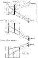
- Figure 4illustrates an autostereoscopic 3D display of the front parallax barrier type comprising an LCD 1 and an electronic parallax barrier in the form of an LCD 2.
- the LCD 1may be of the same type as shown in Figure 1 and comprises a liquid crystal layer 3 which provide a 2D array of pixels for modulating light incident from a light source (not shown) in the direction 5 with spatially multiplexed 2D images recorded from different viewpoints.
- the LCD 2is arranged and controlled so as to act as a parallax barrier providing the transmissive strips or slits such as 4.
- Each slit 4is aligned with a group of columns of pixels with each column of the group displaying a vertically extending strip of a respective 2D image.
- the LCD 2has a barrier electrode pitch which is at least twice the pixel pitch of the LCD 1.
- the structure of the LCD 2is shown in more detail in Figure 5.
- the LCD 2comprises a substrate 11 carrying an electrode arrangement and alignment layer (not shown) and a substrate 12 which carries column electrodes 13 and an alignment layer (not shown).
- a liquid crystal layer 14is disposed between the substrates 11 and 12 and comprises FLC, AFLC, or STN liquid crystal as appropriate.
- the liquid crystal layer 14comprises sharp threshold liquid crystal material and is addressed by a passive matrix electrode arrangement including the column electrodes 13.
- the electrodesare transparent and may be made of indium tin oxide (ITO). There is no black mask.
- Figure 6illustrates the appearance of a small part of the LCD 2 during operation.
- the LCD 2has orthogonally oriented input and output polarisers (not shown in Figure 5).
- column electrodes 15 and 16apply electric fields to the vertically oriented elongate pixels so as to switch the pixels to their clear or transmissive state.
- the column electrodes 15 and 16are substantially transparent but their outlines are shown in Figure 6 for the purpose of illustration.
- fringing fields or suitable electrical pulsesare applied to the electrodes so that the interelectrode gaps 17, 18 and 19 are also switched to the transmissive state.
- a vertically extending transmissive slitis therefore formed and evenly spaced parallel such slits are provided by suitably controlling the LCD 2 so as to form an electronic parallax barrier which in combination with the LCD 1 forms an autostereoscopic display.
- the electrodescause the pixels and the gaps between the pixels within the liquid crystal layer 14 to be switched to the opaque state.
- the edge portions 22may also be switched to the opaque state so that the LCD 1 acts as a parallax barrier comprising a plurality of parallel evenly spaced continuously transparent slits separated by continuously opaque regions such as 20 and 21.
- the electrode arrangement including the electrodes 13, 15 and 16supplies fields such that the whole of the liquid crystal layer 14 is switched to the clear or transmissive state.
- the LCD 2is thus continuously and substantially uniformly transmissive throughout its modulating region.
- the displayoperates as a full resolution 2D display.
- the LCD 2provides good viewing angle performance and good contrast performance without any of the visual artefacts illustrated in Figures 2 and 3.
- low levels of crosstalkare achieved in the 3D mode.
- visual artefactssuch as Moire beating with the pixel structure of the LCD 1 are greatly reduced or eliminated compared with arrangements incorporating black masks, unswitched gaps between electrodes or opaque addressing electrodes within the parallax barrier LCD.
- the parts of the liquid crystal layer 14 in the gaps between the electrodes such as 13have their own switching characteristics as illustrated in Figure 7a, which is ⁇ -V graph for pulses applied to the addressing electrodes.
- the region of the ⁇ -V plane indicated by Ais the switching region for the pixel whereas a region C is the switching region for an adjacent interelectrode gap. Both the pixel and the interelectrode gap are switched in the region B whereas neither is switched in the region D.
- the curves shown in Figure 7arelate to an arrangement having a 4 micrometre interelectrode or interpixel gap with 50 micrometre pixels.
- both horizontal and vertical gapsexist.
- the switching characteristics of the horizontal and vertical gapscan be different if they have a different orientation with respect to the rubbing or alignment direction of the liquid crystal.
- the horizontal and vertical gaps and the pixelcan be controlled as required.
- the gapsmay be switched to be entirely opaque or clear in a separate addressing phase.
- appropriate data and strobe voltagesmay be applied to the same electrodes at different times in order to control the switching of the gap and the pixel independently.
- the width of the interpixel gapsmay also be controlled so as to be appropriate for allowing switching by fringing fields of adjacent electrodes.
- the interpixel gapis preferably between 0.1 and 30 micrometres, and more preferably between 1 and 5 micrometres.
- the addressing signalsare arranged such that both the pixels and the interelectrode gaps are switched in a binary fashion. Thus, no black mask is required to achieve high contrast and low cross talk.
- the liquid crystal layer 14is controlled so that light is transmitted through all parts of the LCD 2. Thus, there is no or substantially no generation of Moire patterns.
- the LCD 1 shown in Figure 4comprises substrates 25 and 26 in addition to the pixellated liquid crystal layer 3.
- the substrates 11, 12, 25 and 26typically comprise glass of thickness 0.7 millimetres
- at least one polariser typically of 0.2 millimetres thicknessis disposed between the liquid crystal layers 3 and 14.
- the pitch of the pixels in the layer 3is typically 80 micrometres.
- the 3D displayproduces viewing zones for the eyes of the observer and the widest parts of these viewing zones are disposed in a plane parallel to the display and are referred to as viewing windows.
- viewing windows of the order of 65 millimetres corresponding to the typical interocular distanceare provided in the plane which is the nominal or best viewing distance for the display. This gives rise to a viewing distance of the order of 850 millimetres. This is relatively large for displays, for instance, of less than 12 inch diagonal size.
- the pitch of the electrodes in the LCD 2is preferably less than 40 micrometres and more preferably less than 11 micrometres.
- Figure 8illustrates a display of the type shown in Figure 4 but in which one of the middle substrates such as 26 has been eliminated.
- the displayis formed as a single device with the substrate 11 being common to the LCDs 1 and 2.
- the consequent reduction in thickness between the layers 3 and 14results in a nominal viewing distance of the order of 350 millimetres, which is more acceptable particularly for displays whose diagonal size is less than 12 inches.
- FIG. 9shows the structure of the display of Figure 8 in more detail.
- the displaycomprises an input polariser 30 for the LCD 1, an internal polariser 31 which acts as an output polariser for the LCD 1 and an input polariser for the LCD 2, and an output polariser 32 for the LCD 2.
- the polarisation absorbing directions of the polarisersare indicated by a dot for a direction normal to the plane of Figure 9 and by an arrow for a direction parallel to the plane of Figure 9.
- the LCD 1further comprises a black mask 33 which covers, for instance, semiconductor structures forming part of the LCD addressing circuitry and which is disposed on or adjacent the substrate 11 between the substrate and the internal polariser 31.
- the substrate 25carries a pixel structure defining layer, for instance in the form of a 2D array of electrodes. Examples of different configurations for defining different pixel configurations are shown at 34 and 35. Suitable colour filters (not shown) may also be provided.
- the arrangement 34comprises a conventional rectangular array of electrodes defining a corresponding array of pixels.
- the arrangement 35defines an arrangement of the type disciosed in EP 0 625 861 such that adjacent columns of pixels are horizontally substantially contiguous.
- the substrate 12carries a parallax structure defining layer 36 in the form of parallel vertically extending column electrodes. Examples of electrode arrangements are described hereinafter.
- the polarisers 30 and 31have substantially orthogonal polarising directions. Similarly, the polarisers 31 and 32 have orthogonal polarising directions. Operation of the LCD 1 will now be described for the case of the TN liquid crystal effect.
- Light from an unpolarised Lambertian light source(not shown) is linearly polarised by the input polariser 30 and passes to the liquid crystal layer 3.
- the pixels of the layer 3selectively rotate the polarisation of light passing therethrough and the internal polariser 31 analyses the output polarisation from the layer 3 in the known way for LCDs.
- Light passing through the LCD 1is thus spatially modulated with spatially multiplexed 2D images.
- the LCD 2is controlled so that transmissive slits 4 are provided and are separated by horizontally contiguous opaque regions such as 37 and 38.
- the region 4rotates the linearly polarised light from the polariser 31 by an amount which is preferably 90 degrees so that the output light passes through the output polariser 32.
- the regions 37 and 38are controlled so as not to rotate the polarisation of light from the internal polariser 31 so that the output polariser 32 blocks the light.
- the transmissive slit 4is effectively aligned with pixel columns indicated at 39, 40 and 41.
- the LCD 2thus acts as a parallax barrier and provides a number of output light cones of wedge-shape (typically two) in which light from the pixel columns 39, 40 and 41 is directed.
- This arrangementis repeated with the relative pitches of the pixel columns of the LCD 1 and the pixels of the LCD 2 being such that a viewpoint corrected display is provided and results in the viewing zones and viewing windows described hereinbefore.
- An observerwhose eyes are disposed in two adjacent viewing zones therefore sees an autostereoscopic 3D image. Each eye of the observer sees typically half of the pixels of the LCD 1 so that the individual 2D images typically have half of the spatial resolution of the LCD 1.
- the layer 36causes the whole of the liquid crystal layer 14 to be switched to a substantially uniformly transmissive state.
- the parallax barrierthus "disappears" and the LCD 2 becomes substantially invisible to an observer.
- both eyes of the observersee the whole of the LCD 1 which may therefore display 2D images at the full spatial resolution of the LCD 1.
- the absence of opaque regions such as black masks or opaque electrodes in the LCD 2substantially eliminates Moire patterns caused by beating with the structure of the LCD 1.
- the ability to produce a clear unadulterated barrier statepermits a full resolution 2D mode which is artefact free to be provided.
- the display shown in Figure 10differs from that shown in Figure 9 in that the internal polariser 31 is disposed between the substrate 11 and the liquid crystal layer 14. Such an arrangement may be favoured by fabrication requirements and operates in the same way as the display of Figure 9.
- Figure 11illustrates an arrangement in which the internal polariser 31 is omitted and the layer 14 comprises FLC incorporating a dye which is aligned with the liquid crystal in a guest-host arrangement. The absorbtion performed by the dye eliminates the need for an internal polariser.
- Light from the unpolarised sourceis polarised by the input polariser 30 and modulated by the liquid crystal layer 3.
- the pixels of the liquid crystal layer 3change the input light to proportions of wanted (W) and unwanted (UW) light polarisations.
- Wwanted
- UWunwanted
- the proportion of unwanted polarisationmust be extinguished for all barrier pixels and this is ensured by the output polariser 32.
- the proportion of wanted polarisationmust also be extinguished for the pixels of the layer 14 which are switched to the opaque state but must be transmitted by the pixels switched to the clear or transmissive state. This is achieved by the effect of the dyed FLC in the layer 14.
- the output polarisation of a standard landscape orientated panel TN active matrix LCD displayis shown typically at 45° to horizontal as shown in Figure 12.
- the polarisation of the LCD 1is aligned with the polarisation of the LCD 2 at their interface.
- the polarisers across the LCD 2are substantially orthogonal.
- the rubbing direction of the FLC alignment layeris at substantially 22.5° to the horizontal and the FLC with usual cone angle of 45° (tilt angle 22.5°) is used.
- the FLCis switchable between two stable states in which the LC molecule is aligned in the directions of the lines D1 and D2.
- one statethe LC molecules are aligned with the input polarisation so that the LC layer has no net effect and the input light is extinguished by the output polariser.
- the LC moleculesare switched to D2 and in this position the anisotropic molecule functions as a waveplate which rotates the plane of polarisation of the input light so as to allow substantial transmission of the input light through the LCD 2.
- Parallel polarisers across the LCD 2will give less contrast but higher transmission.
- FIG 13illustrates the preferred arrangement for the dyed FLC embodiments.
- the LCD 1is configured as above but in this case the LCD 2 uses an FLC which incorporates a dichroic dye, preferably a black dichroic dye in a guest-host configuration.
- the FLChas an unusually high tilt angle of 45 degrees. This is so that, in switching from D1 to D2, the FLC switches between aligned with and being orthogonal to orientations to the input polarisation state. This maximises the difference between the on and off states in this embodiment which does not require an internal polariser.
- Figure 14illustrates that other tilt angles including the standard 22.5° are possible, but in these cases the light transmission is reduced compared with that shown in Figure 13.
- the LCD 1may, for instance, be of the twisted nematic (TN) active matrix type with the black mask 33 controlling the aperture of the pixels.
- the LCD 1 for image displaymay be replaced by other types of devices, such as plasma, plasma addressed liquid crystal (PALC), Field Emission Display and electroluminescent devices.
- the display shown in Figure 15differs from that shown in Figure 10 in that the layer 34, 35 is disposed between the liquid crystal layer 3 and the substrate 11 whereas the black mask 33 is disposed between the layer 3 and the substrate 25.
- Figure 16illustrates an autostereoscopic 3D display of the micropolariser type disclosed in EP 0 721 132.
- the LCD 2differs from that, for instance, shown in Figure 15 in that it has its own input polariser 40 and output substrate 12 but omits the output polariser 32.
- a lenticular sheet 41comprising an array of parallel evenly spaced converging lenticules is disposed on the output face of the substrate 12 to form a backlight.
- the LCD 1 of Figure 16differs from that of Figure 9 in that it has no input or output polariser but has its own substrates 25 and 26.
- the LCD 2receives light 5 from an unpolarised Lambertian light source 5 which is polarised by the input polariser 40.
- the contiguous backlight pixel structure defining layer 36forms a plurality of contiguous pixels within the liquid crystal layer 14 which are elongate, vertical and parallel with alternate pixels supplying output light of orthogonal linear polarisations.
- the lenticular sheet 41generates the viewing zones by directing light from the layer 14 into contiguous light cones or wedges which are modulated by the pixels of the LCD 1.
- the display shown in Figure 16may be used to track movement of an observer so that the viewing zones or windows are maintained at the eyes of the observer, who may therefore perceive a 3D image throughout an enlarged viewing region compared with untracked displays.
- the pixels of the LCD 2are controlled in response to the position of the observer as detected by an observer tracking system.
- the adjacent orthogonally polarising pixelsare effectively moved so that the viewing windows track movements of the observer.
- the pixels of the LCD 2are controlled so as to provide light of uniform polarisation across the LCD 2.
- the observermay therefore view a 2D image with the full spatial resolution of the LCD 1.
- FIG 17differs from that shown in Figure 4 in that the optical order of the LCD 1 and the LCD 2 is reversed. This arrangement therefore acts as a rear parallax barrier 3D autostereoscopic display but otherwise operates in the same way as the display of Figure 4.
- Figure 18illustrates a display which differs from that of Figure 8 in that it is a rear parallax barrier display.
- Figure 19illustrates the structure of the display of Figure 18, which structure differs from that of Figure 9 in the order of components. Operation is as described with respect to Figure 9.
- the display shown in Figure 20differs from that shown in Figure 19 in that the internal polariser 31 is disposed on the other side of the substrate 12.
- Figure 21illustrates a display which differs from that shown in Figure 19 in that the internal polariser 31 is omitted and the liquid crystal layer 14 contains a dye in a guest-host arrangement. Operation of the display shown in Figure 21 is the same as that shown in Figure 11.
- Figure 22shows a display which differs from that shown in Figure 20 in that the positions of the layer 34, 35 and the black mask 33 are interchanged.
- Figure 23shows a display which differs from that shown in Figure 21 in that the layer 14 comprises a liquid crystal layer switchable reflector.
- the layer 14comprises a liquid crystal layer switchable reflector.
- FIGS 24, 25 and 26illustrate embodiments in which the LCD 2 is implemented with a reflective as opposed to an absorptive barrier. This can improve the overall light efficiency of the rear parallax element embodiments.
- the input lightis converted to linear polarisation by the polariser 30, then to circular polarisation by a wideband quarter waveplate 50.
- the LCD 2has a layer 51 comprising a chirped pitch cholesteric switchable reflector.
- the layerIn the barrier mode, the layer has regions of cholesteric reflector and clear (non-cholesteric) states. Switching between these states is accomplished as described hereinbefore. Circular polarisation light impinging on the cholesteric reflector is reflected whereas that impinging on the clear parts is transmitted.
- the transmitted lightis then converted to linear polarisation by a quarter waveplate 52 so as to match the required input polarisation state of the subsequent LCD 1.
- the cholesteric statehas a chirped pitch in order to reflect circular polarisation over both a wide angle and a wide range of wavelengths.
- Figure 25differs from that of Figure 24 by an alternative position for the linear polariser.
- a layer 51a which contains a wide band diffractive reflectoris used as the parallax generating element.
- the sheet reflectoris enabled/disabled in regions required to be transmissive (so as to form a parallax SLM) by controlling the orientation of adjacent anisotropic LC molecules by an electric field in the manner described hereinbefore.
- the gratingis disabled by switching the adjacent LC layer so that there is substantially no refractive index difference between the oriented adjacent LC and the diffractive reflector. This effectively washes out the grating which in these regions becomes invisible.
- the adjacent LCis switched to an orientation in which there is a refractive index difference between the grating and the LC, thereby enabling the reflective function of the grating.
- Figure 27aillustrates an electrode arrangement for the LCD 2 of Figure 5.
- a continuous plane counter electrode 60is disposed on the substrate 11 whereas the parallax structure defining layer 36 has the form of an electrode having formed therein a plurality of slits for corresponding to the parallax barrier slits.
- the arrangementpermits switching between the clear mode and the barrier mode in which the positions of the slits are fixed.
- the LCDmay be switched from one state to another by applying a suitable signal (V on/off).
- Figure 27billustrates an electrode arrangement for the LCD 2 having regions of shared electrodes which permits 2D/3D operation in a number of configurable zones.
- SLMsare suitable for use with mechanical tracking, for instance as disclosed in British Patent Application No. 9619097.0.
- the electrode arrangement shown in Figure 28comprises a continuous plane electrode 60 facing a plurality of parallel uniformly spaced column electrodes such as 61.
- the pixels and interelectrode gapsmay be switched individually by supplying suitable signals V1, V2, ... Vn to the individual electrodes which allows the slit locations of the barrier in the 3D mode to be moved so as to perform electronic tracking, for instance as described hereinafter.
- full resolution 2D zoneswhich extend the full height of the display may be combined with 3D zones by suitably controlling the signals supplied to the electrodes 61.
- Figure 29illustrates an XY passive matrix addressing arrangement comprising column electrodes such as 61 and row electrodes such 62.
- Strobe signals Vr1, Vr2, ... Vrnmay be applied in sequence to the electrodes 62 so as to enter data in accordance with the column signals V1, ... Vn a row at a time so as to refresh the mode of the display.
- the gaps between pixelsmay be controlled by fringing fields or by "frame ahead gap blanking". Alternatively, the gaps may be switched by different strobe and data voltages applied to the same row and column electrodes and optionally to other row and column electrodes without altering the state of the adjacent pixels.
- FIG. 29may be used to provide any desired configuration of 2D and 3D image zones simultaneously.
- Figure 30illustrates a 3D background 63 having 2D image zones 64, 65 and 66.
- the 2D zone 66has an inset 3D image zone 67.
- the corresponding pixels of the LCD 2are controlled to provide parallax barriers whereas the pixels in the regions of the 2D zones are controlled to be transmissive.
- the presence of the parallax barrier over the 3D regionsgives a difference in intensity between the 2D and 3D zones which may be compensated for electronically in the drive signal. Compensation by setting the 2D zones to an intermediate attenuating grey level may be used to achieve the same effect but is not appropriate for the LCD 2 when using binary switching effects, for instance in the case of standard FLCs.
- the presence of a border around an inset 2D or 3D image zoneprevents vertical parallax caused by the separation of the LCDs 1 and 2 seen by a viewer above or below the axis of the display from making the edge pixels of an inset zone appear in the wrong image zone.
- Figure 31shows a temporally multiplexed 3D autostereoscopic display in which the image LCD is a fast SLM, for instance of the FLC type, and the parallax barrier LCD is likewise of the fast switching type such as FLC.
- the middle part of Figure 31illustrates the generation of a left eye viewing window 70 during a first field in which image data of a first 2D image are displayed by the LCD 1.
- the windowsare produced in a plurality of lobes as is known in 3D display technology.
- the slits 4 of the parallax barrier formed by the LCD 2are located in a first lateral position with respect to the pixels of the LCD 1.
- FIG. 31illustrates generation of right eye viewing windows 71.
- a second field of image data representing an image to be viewed by the right eye of the observeris displayed by the LCD 1.
- the LCD 2is controlled so that the pixels 4 have a different lateral position with respect to the pixels of the LCD 1.
- Figure 32illustrates a temporally multiplexed display which differs from that shown in Figure 31 in that the optical order of the fast SLM 1 and the dynamic parallax barrier LCD 2 are reversed.
- Figure 33illustrates use of the steerable backlight shown in Figure 16 in a temporally multiplexed display.
- 2D image dataare supplied in sequence to the fast SLM 1 and the LCD 2 is controlled such that light corresponding to each 2D image is directed to a respective one of the viewing windows 70 and 71.
- Figure 34illustrates an arrangement combining spatial and temporal multiplexing to provide four viewing windows 72 to 75.
- two spatially multiplexed 2D imagesare displayed by the SLM 1.
- two viewing windows 73 and 75are provided in one field whereas two viewing windows 72 and 74 are provided in the next field.
- the display of Figure 35differs from that shown in Figure 34 in that the optical order of the SLM 1 and the barrier 2 is reversed.
- Figure 36illustrates a display of the type shown in Figure 9 for providing a pair of viewing windows for a first observer and another pair of viewing windows for a second observer. The creation of the individual viewing windows is shown in the middle and lower parts of Figure 36.
- the slits in the two fields of the displays shown in Figures 32 and 35need not be contiguous with each other. Further, the width of the slits can be electrically adjusted to control brightness against viewing window quality, which is a measure of 3D crosstalk level.
- Figure 38illustrates this for a pixel aperture 76 of rectangular shape and for a narrow slit 77 and a wide slit 78.
- the variation of intensity with observer position for the slits 77 and 78is illustrated at 79 and 80, respectively.
- the profile 79shows that the intensity of light is reduced but the window shape is better.
- the corresponding intensity profile 80shows greater intensity but a worse window shape.
- FIG 37illustrates different tracking modes for an LCD 2 of the type shown in Figure 5.
- Each slitis made up of a number of pixels and will be illustrated for the case of four pixels.
- the four pixelsare controlled so as to be transparent.
- the pixelsmay be switched such that one pixel at one edge of the slit is switched to black as one pixel next to the other edge of the slit is switched to white. This provides one step tracking and minimises flicker.
- Optical performanceis optimum for one step tracking in that undesirable visible artefacts are minimised and this therefore represents the normal operation.
- the middle part of Figure 37illustrates two step tracking in which two pixels at one edge are switched to black as two pixels adjacent the other edge are switched to white. This mode of tracking allows for higher speed observer movements to be accommodated.
- Figure 37illustrates jump tracking in which no pixels remain clear i.e. the location of the transmissive slit jumps so that there is no overlap between one slit position and the next slit position. This mode allows for extreme observer movement and for error recovery.
Landscapes
- Engineering & Computer Science (AREA)
- Multimedia (AREA)
- Signal Processing (AREA)
- Physics & Mathematics (AREA)
- General Physics & Mathematics (AREA)
- Optics & Photonics (AREA)
- Liquid Crystal (AREA)
- Devices For Indicating Variable Information By Combining Individual Elements (AREA)
- Transforming Electric Information Into Light Information (AREA)
- Testing, Inspecting, Measuring Of Stereoscopic Televisions And Televisions (AREA)
Abstract
Description
Claims (24)
- A spatial light modulator characterised by a modulatorregion which is switchable between a clear mode, in which the region isof substantially uniform transmissivity, and a barrier mode, in which theregion has a plurality of evenly spaced parallel transmissive strips (15-19)extending in a first direction and separated by continuous substantiallyopaque sub-regions (20, 21).
- A modulator as claimed in Claim 1, characterised in thatthe region comprises a plurality of elongate picture elements extending inthe first direction.
- A modulator as claimed in Claim 2, characterised in thatthe picture elements are switchable together to opaque to define the sub-regions(20, 21) and are spaced apart to define the transmissive slits.
- A modulator as claimed in Claim 2, characterised in thatthe picture elements define gaps (17-19) therebetween, which gaps areswitchable between transmissive and opaque independently of the pictureelements.
- A modulator as claimed in Claim 1, characterisd in that theregion comprises a two dimensional array of picture elements, each ofwhich is independently switchable between transmissive and opaque andwhich define gaps therebetween, which gaps are switchable betweentransmissive and opaque.
- A modulator as claimed in Claim 5, characterised in thatthe gaps are independently switchable between transmissive and opaque.
- A modulator as claimed in any one of the precedingclaims, characterised by a liquid crystal device (2) including a first layer(14) of liquid crystal material.
- A modulator as claimed in Claim 7, characterised in thatthe first layer (14) comprises ferroelectric liquid crystal material.
- A modulator as claimed in Claim 7, characterised in thatthe first layer (14) comprises anti-ferroelectric liquid crystal material.
- A modulator as claimed in Claim 7, characterised in thatthe first layer (14) comprises super-twisted nematic liquid crystal material.
- A modulator as claimed in any one of Claims 7 to 10,characterised in that the first layer (14) includes an anistropic dye.
- A modulator as claimed in any one of Claims 7 to 11 whendependent on any one of Claims 2 to 6, characterised in that the pictureelements are defined by addressing electrodes (13, 15, 16, 36, 60-62).
- A modulator as claimed in Claim 12, characterised in thatthe addressing electrodes (13, 15, 16, 36, 60-62) comprise a passivematrix addressing arrangement.
- A modulator as claimed in Claim 12 or 13, whendependent on any one of Claims 4 to 6, charactertised in that the gaps (17-19)are switchable by means of fringing fields.
- A modulator as claimed in any one of the precedingclaims, characterised in that the opaque sub-regions are reflective.
- A spatial light modulator characterised by a modulatorregion which is switchable between a first mode in which the region isarranged to supply light of a substantially uniform first polarisation, and asecond mode, in which the region is arranged to supply light of the firstpolarisation in a plurality of evenly spaced parallel strips and to supplylight of a second polarisation, different from the first polarisation, incontinuous sub-regions which separate the strips.
- A modulator as claimed in Claim 16, characterised in thatthe second polarisation is orthogonal to the first polarisation.
- A directional display characterised by a modulator (2) asclaimed in any one of the preceding claims cooperating with an imagedisplay (1).
- A display as claimed in Claim 18, characterised in that theimage display (1 ) comprises a further spatial light modulator.
- A display as claimed in Claim 19, characterised in that thefurther spatial light modulator (1) comprises a further liquid crystal deviceincluding a second layer (3) of liquid crystal material.
- A display as claimed in Claim 20, characterised by first andsecond substrates (12, 11) with the first layer (14) therebetween and a thirdsubstrate (25) with the second layer (3) between the second and thirdsubstrates (11, 25).
- A display as claimed in Claim 20 or 21 when notdependent on Claim 11, characterised by a single polariser (31) betweenthe first and second layers (14, 3).
- A directional light source characterised by a modulator (2)as claimed in any one of Claims 1 to 17 cooperating with a diffuse lightsource (5).
- A light source as claimed in Claim 23, chracterised by alenticular sheet (41) having lenticules extending in the first direction.
Applications Claiming Priority (2)
| Application Number | Priority Date | Filing Date | Title |
|---|---|---|---|
| GB9620210AGB2317710A (en) | 1996-09-27 | 1996-09-27 | Spatial light modulator and directional display |
| GB9620210 | 1996-09-27 |
Publications (2)
| Publication Number | Publication Date |
|---|---|
| EP0833183A1true EP0833183A1 (en) | 1998-04-01 |
| EP0833183B1 EP0833183B1 (en) | 2004-06-23 |
Family
ID=10800619
Family Applications (1)
| Application Number | Title | Priority Date | Filing Date |
|---|---|---|---|
| EP97307571AExpired - LifetimeEP0833183B1 (en) | 1996-09-27 | 1997-09-26 | LCD spatial light modulator as electronic parallax barrier |
Country Status (5)
| Country | Link |
|---|---|
| US (1) | US5969850A (en) |
| EP (1) | EP0833183B1 (en) |
| JP (1) | JPH10142572A (en) |
| DE (1) | DE69729617T2 (en) |
| GB (1) | GB2317710A (en) |
Cited By (76)
| Publication number | Priority date | Publication date | Assignee | Title |
|---|---|---|---|---|
| WO1999059021A1 (en)* | 1998-05-12 | 1999-11-18 | Sharp Kabushiki Kaisha | Directional display |
| WO2002005014A1 (en)* | 2000-07-12 | 2002-01-17 | Street Graham S B | Structured light source |
| WO2003049072A1 (en)* | 2001-12-04 | 2003-06-12 | Koninklijke Philips Electronics N.V. | Directional image display |
| EP1401216A2 (en) | 2002-09-17 | 2004-03-24 | Sharp Kabushiki Kaisha | Autostereoscopic display |
| WO2004040354A1 (en) | 2002-10-30 | 2004-05-13 | Semiconductor Energy Laboratory Co., Ltd. | Display unit and electronic equipment |
| US6831624B1 (en) | 1999-01-15 | 2004-12-14 | Sharp Kabushiki Kaisha | Time sequentially scanned display |
| WO2004092775A3 (en)* | 2003-04-16 | 2005-03-17 | X3D Technologies Gmbh | Arrangement for two-dimensional or three-dimensional representation |
| WO2005045488A1 (en)* | 2003-11-07 | 2005-05-19 | Koninklijke Philips Electronics N.V. | Waveguide for autostereoscopic display |
| DE102004014906A1 (en)* | 2004-03-23 | 2005-10-13 | X3D Technologies Gmbh | Selective image e.g. two-dimensional image, projecting arrangement for electronic device, has two displays operating in two modes, where one display partly reproduces white image and other display presents two-dimensional image in one mode |
| GB2415849A (en)* | 2004-06-29 | 2006-01-04 | Sharp Kk | A switchable liquid crystal parallax barrier |
| WO2005106563A3 (en)* | 2004-05-05 | 2006-03-16 | Juergen Spielberger | System for observing stereoscopic images |
| EP1250013A4 (en)* | 1999-09-02 | 2006-05-24 | Obschestvo S Ogranichennoi Otv | Method for displaying the image of an object |
| EP1662808A1 (en)* | 2004-11-30 | 2006-05-31 | Samsung SDI Co., Ltd. | Barrier device and stereoscopic image display using the same |
| EP1708515A1 (en)* | 2005-03-30 | 2006-10-04 | Sanyo Epson Imaging Devices Corporation | Liquid crystal display device with which a plurality of observers can visually recognize each of two different images displayed on a single LCD panel |
| EP1708516A1 (en)* | 2005-03-31 | 2006-10-04 | Sanyo Epson Imaging Devices Corporation | Image display |
| EP1739978A3 (en)* | 2005-06-29 | 2007-03-14 | Samsung SDI Co., Ltd. | Parallax barrier and three dimensional display device using the same |
| US7215475B2 (en) | 2003-07-10 | 2007-05-08 | Ocuity Limited | Lens array structure |
| EP1793623A1 (en)* | 2005-11-30 | 2007-06-06 | Samsung SDI Co., Ltd. | Autostereoscopic display with parallax barrier formed with a liquid crystal display of a normally black mode of transmission |
| EP1775966A3 (en)* | 2005-10-12 | 2007-08-15 | LG Electronics Inc. | System and method for displaying three-dimensional image |
| WO2006134554A3 (en)* | 2005-06-14 | 2007-09-13 | Koninkl Philips Electronics Nv | Combined single/multiple view-display |
| WO2007069131A3 (en)* | 2005-12-14 | 2007-09-20 | Koninkl Philips Electronics Nv | 2d/3d autostereoscopic display device |
| US7359105B2 (en) | 2006-02-07 | 2008-04-15 | Sharp Kabushiki Kaisha | Spatial light modulator and a display device |
| EP1942681A1 (en)* | 2007-01-05 | 2008-07-09 | Samsung Electronics Co., Ltd. | Highly efficient 2D/3D switchable autostereoscopic display device |
| CN100403806C (en)* | 2003-04-17 | 2008-07-16 | Lg电子有限公司 | 3D image display device |
| EP1956415A2 (en) | 2007-02-07 | 2008-08-13 | Samsung Electronics Co., Ltd. | 2D-3D image switching display system |
| US7423796B2 (en) | 2003-09-30 | 2008-09-09 | Au Optronics Corporation | Directional display apparatus |
| US7426068B2 (en) | 2005-01-10 | 2008-09-16 | Au Optronics Corporation | Display apparatus |
| US7471352B2 (en) | 2003-07-10 | 2008-12-30 | Au Optronics Corp. | Directional display apparatus |
| WO2009040097A1 (en)* | 2007-09-25 | 2009-04-02 | Visumotion Gmbh | Method and arrangement for spatial illustration |
| US7532272B2 (en) | 2003-02-05 | 2009-05-12 | Au Optronics Corp. | Switchable lens |
| US7612859B2 (en) | 2005-10-31 | 2009-11-03 | Hewlett-Packard Development Company, L.P. | Ultra-violet radiation absorbing grid |
| EP1923860A3 (en)* | 2006-11-19 | 2010-01-13 | Barco NV | Defect compensation and/or masking |
| US7876400B2 (en) | 2005-10-31 | 2011-01-25 | Hewlett-Packard Development Company, L.P. | Optical modulation system |
| US20110109623A1 (en)* | 2009-11-12 | 2011-05-12 | Ingo Relke | Parallax barrier filter |
| US7986375B2 (en) | 2006-08-17 | 2011-07-26 | Koninklijke Philips Electronics N.V. | Multi-view autostereoscopic display device having particular driving means and driving method |
| EP2357630A1 (en)* | 2009-12-31 | 2011-08-17 | Broadcom Corporation | Display with adaptable parallax barrier |
| EP1938140A4 (en)* | 2005-08-26 | 2012-01-11 | Masterimage 3D Asia Llc | CELL-TYPE PARALLAX BARRIER AND STEREOSCOPIC IMAGE DISPLAY APPARATUS USING SAID BARRIER |
| US8115805B2 (en) | 2004-02-25 | 2012-02-14 | Samsung Mobile Display Co., Ltd. | Stereoscopic image display device and method for driving the same |
| WO2012076702A1 (en)* | 2010-12-09 | 2012-06-14 | Seereal Technologies S.A. | Light modulation device for a display |
| EP2487917A3 (en)* | 2011-02-14 | 2012-08-29 | Sony Corporation | Display device and display method |
| CN102967941A (en)* | 2011-08-30 | 2013-03-13 | 索尼公司 | Display device and electronic unit |
| EP2014103A4 (en)* | 2006-05-04 | 2013-05-15 | Samsung Electronics Co Ltd | MULTI-VIEW AUTOSTEREOSCOPIC DISPLAY |
| EP2597879A3 (en)* | 2011-11-22 | 2013-12-25 | LG Electronics Inc. | Three-dimensional image processing apparatus and calibration method of the same |
| WO2014064588A3 (en)* | 2012-10-26 | 2014-07-24 | Koninklijke Philips N.V. | Autostereoscopic display device having a transparent mode of operation |
| US8823782B2 (en) | 2009-12-31 | 2014-09-02 | Broadcom Corporation | Remote control with integrated position, viewer identification and optical and audio test |
| US8854531B2 (en) | 2009-12-31 | 2014-10-07 | Broadcom Corporation | Multiple remote controllers that each simultaneously controls a different visual presentation of a 2D/3D display |
| EP2850481A4 (en)* | 2012-05-18 | 2015-11-11 | Reald Inc | CONTROL SYSTEM FOR DIRECTIONAL LIGHT SOURCE |
| US9201255B2 (en) | 2010-03-19 | 2015-12-01 | Nokia Technologies Oy | Apparatus, methods and computer programs for configuring output of a display |
| US9247286B2 (en) | 2009-12-31 | 2016-01-26 | Broadcom Corporation | Frame formatting supporting mixed two and three dimensional video data communication |
| US9280042B2 (en) | 2012-03-16 | 2016-03-08 | City University Of Hong Kong | Automatic switching of a multi-mode projector display screen for displaying three-dimensional and two-dimensional images |
| US9678267B2 (en) | 2012-05-18 | 2017-06-13 | Reald Spark, Llc | Wide angle imaging directional backlights |
| US9709723B2 (en) | 2012-05-18 | 2017-07-18 | Reald Spark, Llc | Directional backlight |
| US9739928B2 (en) | 2013-10-14 | 2017-08-22 | Reald Spark, Llc | Light input for directional backlight |
| US9740034B2 (en) | 2013-10-14 | 2017-08-22 | Reald Spark, Llc | Control of directional display |
| US9835792B2 (en) | 2014-10-08 | 2017-12-05 | Reald Spark, Llc | Directional backlight |
| US9872007B2 (en) | 2013-06-17 | 2018-01-16 | Reald Spark, Llc | Controlling light sources of a directional backlight |
| US9910207B2 (en) | 2012-05-18 | 2018-03-06 | Reald Spark, Llc | Polarization recovery in a directional display device |
| US10054732B2 (en) | 2013-02-22 | 2018-08-21 | Reald Spark, Llc | Directional backlight having a rear reflector |
| US10091487B2 (en) | 2013-08-22 | 2018-10-02 | Roberto Massaru Amemiya | Real image camcorder, glass-free 3D display and processes for capturing and reproducing 3D media using parallel ray filters |
| US10228505B2 (en) | 2015-05-27 | 2019-03-12 | Reald Spark, Llc | Wide angle imaging directional backlights |
| US10321123B2 (en) | 2016-01-05 | 2019-06-11 | Reald Spark, Llc | Gaze correction of multi-view images |
| US10330843B2 (en) | 2015-11-13 | 2019-06-25 | Reald Spark, Llc | Wide angle imaging directional backlights |
| US10356383B2 (en) | 2014-12-24 | 2019-07-16 | Reald Spark, Llc | Adjustment of perceived roundness in stereoscopic image of a head |
| US10359561B2 (en) | 2015-11-13 | 2019-07-23 | Reald Spark, Llc | Waveguide comprising surface relief feature and directional backlight, directional display device, and directional display apparatus comprising said waveguide |
| US10359560B2 (en) | 2015-04-13 | 2019-07-23 | Reald Spark, Llc | Wide angle imaging directional backlights |
| US10365426B2 (en) | 2012-05-18 | 2019-07-30 | Reald Spark, Llc | Directional backlight |
| US10459321B2 (en) | 2015-11-10 | 2019-10-29 | Reald Inc. | Distortion matching polarization conversion systems and methods thereof |
| US10475418B2 (en) | 2015-10-26 | 2019-11-12 | Reald Spark, Llc | Intelligent privacy system, apparatus, and method thereof |
| US10587867B2 (en) | 2015-07-14 | 2020-03-10 | Sharp Kabushiki Kaisha | Parallax barrier with independently controllable regions |
| US10587866B2 (en) | 2015-07-14 | 2020-03-10 | Sharp Kabushiki Kaisha | Parallax barrier with independently controllable regions |
| US11067736B2 (en) | 2014-06-26 | 2021-07-20 | Reald Spark, Llc | Directional privacy display |
| US11287878B2 (en) | 2012-05-18 | 2022-03-29 | ReaID Spark, LLC | Controlling light sources of a directional backlight |
| US11821602B2 (en) | 2020-09-16 | 2023-11-21 | Reald Spark, Llc | Vehicle external illumination device |
| US11966049B2 (en) | 2022-08-02 | 2024-04-23 | Reald Spark, Llc | Pupil tracking near-eye display |
| WO2024156922A1 (en)* | 2023-01-27 | 2024-08-02 | Realfiction Lab Aps | Hybrid scan display |
| US12282168B2 (en) | 2022-08-11 | 2025-04-22 | Reald Spark, Llc | Anamorphic directional illumination device with selective light-guiding |
Families Citing this family (132)
| Publication number | Priority date | Publication date | Assignee | Title |
|---|---|---|---|---|
| JPH10221646A (en)* | 1997-02-10 | 1998-08-21 | Canon Inc | 3D image display device |
| US6710920B1 (en)* | 1998-03-27 | 2004-03-23 | Sanyo Electric Co., Ltd | Stereoscopic display |
| US20020101658A1 (en)* | 2001-01-29 | 2002-08-01 | Reuben Hoppenstein | Electronic virtual lens for observing 3-D or 4-D images |
| GB2390948A (en)* | 2002-07-17 | 2004-01-21 | Sharp Kk | Autostereoscopic display |
| JPWO2004011987A1 (en)* | 2002-07-29 | 2005-11-24 | シャープ株式会社 | Substrate with parallax barrier layer, method for manufacturing substrate with parallax barrier layer, and three-dimensional display device |
| US20040017347A1 (en)* | 2002-07-29 | 2004-01-29 | Hougham Gareth G. | Method for fabricating color pixels without light filters |
| ATE384633T1 (en)* | 2002-08-19 | 2008-02-15 | Koninkl Philips Electronics Nv | DISPLAY SYSTEM FOR DISPLAYING IMAGES IN A VEHICLE |
| JP4138747B2 (en)* | 2002-08-27 | 2008-08-27 | シャープ株式会社 | Content playback device capable of playing content in optimal playback mode |
| WO2004029704A1 (en)* | 2002-09-26 | 2004-04-08 | Sharp Kabushiki Kaisha | Reflective/transmissive type liquid crystal display panel, 2d/3d switching liquid crystal display panel, and 2d/3d switching liquid crystal display unit |
| JP4087322B2 (en)* | 2002-09-26 | 2008-05-21 | シャープ株式会社 | Liquid crystal display panel and liquid crystal display device |
| WO2004075526A2 (en)* | 2003-02-21 | 2004-09-02 | Koninklijke Philips Electronics N.V. | Autostereoscopic display |
| WO2004088995A1 (en)* | 2003-03-31 | 2004-10-14 | Koninklijke Philips Electronics N.V. | Autostereoscopic display |
| GB2403863A (en)* | 2003-07-10 | 2005-01-12 | Ocuity Ltd | Colour pixel configuration for an autostereoscopic display |
| KR100970721B1 (en)* | 2003-07-29 | 2010-07-16 | 삼성전자주식회사 | High resolution three dimensional image display |
| GB2406731A (en)* | 2003-08-30 | 2005-04-06 | Sharp Kk | Multiple view display having directional backlight |
| GB2405542A (en)* | 2003-08-30 | 2005-03-02 | Sharp Kk | Multiple view directional display having display layer and parallax optic sandwiched between substrates. |
| US7649688B2 (en)* | 2003-10-08 | 2010-01-19 | Louis Racette | Auto-stereo three-dimensional images |
| US20050088516A1 (en)* | 2003-10-23 | 2005-04-28 | Myoung-Seop Song | Display device for both two-dimensional and three-dimensional images and display method thereof |
| GB0400370D0 (en)* | 2004-01-09 | 2004-02-11 | Koninkl Philips Electronics Nv | Display device for volumetric imaging using a birefringent optical path length adjuster |
| GB0400372D0 (en)* | 2004-01-09 | 2004-02-11 | Koninkl Philips Electronics Nv | Optical path length adjuster |
| DE102004004282A1 (en)* | 2004-01-28 | 2005-09-08 | Siemens Ag | Autostereoscopic display |
| CN100345029C (en)* | 2004-02-13 | 2007-10-24 | 胜华科技股份有限公司 | A display system that can switch between two-dimensional and three-dimensional images |
| GB0403933D0 (en)* | 2004-02-21 | 2004-03-24 | Koninkl Philips Electronics Nv | Optical path length adjuster |
| GB0403932D0 (en)* | 2004-02-21 | 2004-03-24 | Koninkl Philips Electronics Nv | Improving image quality in a 3D image display device |
| GB0404372D0 (en)* | 2004-02-27 | 2004-03-31 | Koninkl Philips Electronics Nv | Liquid crystal display |
| JP4024769B2 (en)* | 2004-03-11 | 2007-12-19 | シャープ株式会社 | Liquid crystal display panel and liquid crystal display device |
| JP2005274905A (en)* | 2004-03-24 | 2005-10-06 | Sanyo Electric Co Ltd | Three-dimensional image display device |
| US20050212984A1 (en)* | 2004-03-26 | 2005-09-29 | Yi-Chun Wu | Dual-mode display system for 2D and 3D viewing |
| US20050219693A1 (en)* | 2004-04-02 | 2005-10-06 | David Hartkop | Scanning aperture three dimensional display device |
| WO2005106572A1 (en)* | 2004-04-02 | 2005-11-10 | David Hartkop | Scanning aperture three dimensional display device |
| WO2006068426A1 (en)* | 2004-12-22 | 2006-06-29 | Master Image Co., Ltd. | Parallax-barrier type stereoscopic display apparatus |
| KR101087568B1 (en)* | 2004-12-30 | 2011-11-28 | 엘지디스플레이 주식회사 | Parallax barrier liquid crystal panel for stereoscopic image display device and manufacturing method |
| TWI264600B (en)* | 2005-02-03 | 2006-10-21 | Au Optronics Corp | 2D/3D display and method for forming 3D images |
| JP2006260853A (en)* | 2005-03-15 | 2006-09-28 | Fuji Photo Film Co Ltd | Lighting device |
| JP4934974B2 (en)* | 2005-03-17 | 2012-05-23 | エプソンイメージングデバイス株式会社 | Image display device |
| EP2268050A3 (en) | 2005-05-31 | 2015-11-11 | Epson Imaging Devices Corporation | Image display |
| KR101170911B1 (en)* | 2005-06-30 | 2012-08-03 | 엘지디스플레이 주식회사 | Liquid crystal display and method for fabricating the same |
| US20080211978A1 (en)* | 2005-07-08 | 2008-09-04 | Koninklijke Philips Electronics, N.V. | Controlling Shape and Direction of Light |
| KR100813977B1 (en)* | 2005-07-08 | 2008-03-14 | 삼성전자주식회사 | High resolution 2D-3D switchable autostereoscopic display apparatus |
| GB2428345A (en)* | 2005-07-13 | 2007-01-24 | Sharp Kk | A display having multiple view and single view modes |
| US7518664B2 (en)* | 2005-09-12 | 2009-04-14 | Sharp Kabushiki Kaisha | Multiple-view directional display having parallax optic disposed within an image display element that has an image display layer sandwiched between TFT and color filter substrates |
| US7813042B2 (en)* | 2005-09-12 | 2010-10-12 | Sharp Kabushiki Kaisha | Multiple-view directional display |
| US20090303157A1 (en)* | 2005-09-16 | 2009-12-10 | Akira Imai | Display device |
| JP4254782B2 (en)* | 2005-11-21 | 2009-04-15 | エプソンイメージングデバイス株式会社 | Image display device and electronic device |
| US8330881B2 (en)* | 2005-12-20 | 2012-12-11 | Koninklijke Philips Electronics N.V. | Autostereoscopic display device |
| KR101210887B1 (en)* | 2005-12-22 | 2012-12-11 | 엘지디스플레이 주식회사 | Liquid Crystal Display Device and Driving Method Thereof |
| KR101291860B1 (en)* | 2005-12-28 | 2013-07-31 | 엘지디스플레이 주식회사 | 2-dimension image and 3-dimension image display device and manufacturing for display device thereof |
| KR101281906B1 (en)* | 2005-12-29 | 2013-07-03 | 엘지디스플레이 주식회사 | 2-dimension image and 3-dimension image display device and manufacturing for display device thereof |
| JP4215058B2 (en)* | 2006-01-19 | 2009-01-28 | エプソンイメージングデバイス株式会社 | Image display device and electronic device |
| KR100813975B1 (en)* | 2006-02-27 | 2008-03-14 | 삼성전자주식회사 | High resolution 2D-3D switchable autostereoscopic display apparatus |
| JP4548379B2 (en)* | 2006-03-31 | 2010-09-22 | カシオ計算機株式会社 | 3D image display device |
| KR100893616B1 (en)* | 2006-04-17 | 2009-04-20 | 삼성모바일디스플레이주식회사 | Electronic video equipment, 2D / 3D video display device and driving method thereof |
| CN101356832B (en)* | 2006-05-04 | 2011-06-22 | 三星电子株式会社 | High resolution autostereoscopic display device with interlaced images |
| KR101255209B1 (en) | 2006-05-04 | 2013-04-23 | 삼성전자주식회사 | Hihg resolution autostereoscopic display apparatus with lnterlaced image |
| KR100765131B1 (en) | 2006-05-12 | 2007-10-22 | (주)엔디스 | Wide viewing angle stereoscopic display |
| US7791686B2 (en)* | 2006-06-23 | 2010-09-07 | Waterstrike Incorporated | LCD-based confidential viewing apparatus utilizing auto-inversion masking |
| KR101275142B1 (en)* | 2006-08-08 | 2013-06-14 | 삼성전자주식회사 | High resolution 2D/3D switchable display apparatus |
| CN101512415B (en)* | 2006-09-07 | 2012-06-06 | 夏普株式会社 | Image display device, electronic device, and parallax barrier element |
| JP4981394B2 (en)* | 2006-09-28 | 2012-07-18 | 株式会社ジャパンディスプレイイースト | Display device |
| KR100856414B1 (en)* | 2006-12-18 | 2008-09-04 | 삼성전자주식회사 | Stereoscopic video display |
| KR100786468B1 (en)* | 2007-01-02 | 2007-12-17 | 삼성에스디아이 주식회사 | 2D and 3D image selectable display device |
| CA2576846A1 (en)* | 2007-02-02 | 2008-08-02 | General Electric Canada | Reversing switch |
| KR20080086110A (en)* | 2007-03-21 | 2008-09-25 | 삼성전자주식회사 | High efficiency 2D / 3D video display device |
| US20080239483A1 (en)* | 2007-03-30 | 2008-10-02 | Arisawa Mfg. Co., Ltd. | Stereoscopic displaying apparatus |
| RU2377623C2 (en)* | 2007-04-20 | 2009-12-27 | Василий Александрович ЕЖОВ | Method of viewing stereo images with complete resolution for each aspect and device to this end |
| KR101545008B1 (en)* | 2007-06-26 | 2015-08-18 | 코닌클리케 필립스 엔.브이. | Method and system for encoding a 3d video signal, enclosed 3d video signal, method and system for decoder for a 3d video signal |
| KR101339768B1 (en)* | 2007-08-30 | 2013-12-11 | 삼성전자주식회사 | Plane light source and lcd backlight unit comprising the same |
| KR100908724B1 (en)* | 2007-10-22 | 2009-07-22 | 삼성모바일디스플레이주식회사 | Barrier device and electronic imaging device including the same |
| WO2009105544A2 (en)* | 2008-02-19 | 2009-08-27 | The Board Of Trustees Of The University Of Illinois | Large format high resolution interactive display |
| CN102132573B (en) | 2008-08-26 | 2013-10-23 | 皇家飞利浦电子股份有限公司 | Method and system for encoding 3d video signal, encoder for encoding 3-d video signal, encoded 3d video signal, method and system for decoding 3d video signal, decoder for decoding 3d video signal |
| TWI381205B (en)* | 2008-10-15 | 2013-01-01 | Au Optronics Corp | Switchable barrier and falt display panel |
| US8587639B2 (en)* | 2008-12-11 | 2013-11-19 | Alcatel Lucent | Method of improved three dimensional display technique |
| US20100194861A1 (en)* | 2009-01-30 | 2010-08-05 | Reuben Hoppenstein | Advance in Transmission and Display of Multi-Dimensional Images for Digital Monitors and Television Receivers using a virtual lens |
| KR101324440B1 (en)* | 2009-02-11 | 2013-10-31 | 엘지디스플레이 주식회사 | Method of controlling view of stereoscopic image and stereoscopic image display using the same |
| WO2010106463A1 (en)* | 2009-03-17 | 2010-09-23 | Koninklijke Philips Electronics N.V. | Methods of driving colour sequential displays |
| US8704877B2 (en)* | 2010-02-01 | 2014-04-22 | Eldon Technology Limited | Systems and methods for presenting three-dimensional content using apertures |
| JP2011169949A (en)* | 2010-02-16 | 2011-09-01 | Hitachi Displays Ltd | Three-dimensional image display device |
| US20110234605A1 (en)* | 2010-03-26 | 2011-09-29 | Nathan James Smith | Display having split sub-pixels for multiple image display functions |
| TW201141194A (en)* | 2010-05-14 | 2011-11-16 | Ind Tech Res Inst | Three dimensional display device and three dimensional system |
| JP5073013B2 (en)* | 2010-06-11 | 2012-11-14 | 任天堂株式会社 | Display control program, display control device, display control method, and display control system |
| US8872990B2 (en) | 2010-07-12 | 2014-10-28 | Sharp Kabushiki Kaisha | Display device |
| TWI439730B (en) | 2010-07-16 | 2014-06-01 | Au Optronics Corp | Parallax barrier and application thereof |
| JP5568409B2 (en)* | 2010-08-24 | 2014-08-06 | 株式会社日立製作所 | 3D display device |
| JP6111197B2 (en)* | 2010-10-01 | 2017-04-05 | サムスン エレクトロニクス カンパニー リミテッド | 3D display device using barrier and driving method thereof |
| TWI431326B (en) | 2010-10-29 | 2014-03-21 | Au Optronics Corp | Two-dimension and stereo display device and driving method thereof |
| KR101670927B1 (en)* | 2010-11-05 | 2016-11-01 | 삼성전자주식회사 | Display apparatus and method |
| KR101732131B1 (en) | 2010-11-12 | 2017-05-04 | 삼성전자주식회사 | Image providing apparatus and image providng method based on user's location |
| US20130328866A1 (en)* | 2010-11-19 | 2013-12-12 | Reald Inc. | Spatially multiplexed imaging directional backlight displays |
| KR20120069432A (en) | 2010-12-20 | 2012-06-28 | 삼성전자주식회사 | 3d image display apparatus and driving method thereof |
| DE112011104705T5 (en)* | 2011-01-12 | 2013-10-31 | Arisawa Mfg. Co., Ltd. | Stereoscopic image display device |
| TW201232039A (en)* | 2011-01-28 | 2012-08-01 | Chunghwa Picture Tubes Ltd | Stereoscopic display device with changeable barrier patterns |
| KR20120091585A (en)* | 2011-02-09 | 2012-08-20 | 삼성전기주식회사 | Display device and method for providing 3d image of the display device |
| TWI569041B (en) | 2011-02-14 | 2017-02-01 | 半導體能源研究所股份有限公司 | Display device |
| US9443455B2 (en) | 2011-02-25 | 2016-09-13 | Semiconductor Energy Laboratory Co., Ltd. | Display device having a plurality of pixels |
| US9558687B2 (en) | 2011-03-11 | 2017-01-31 | Semiconductor Energy Laboratory Co., Ltd. | Display device and method for driving the same |
| JP2014139593A (en)* | 2011-05-09 | 2014-07-31 | Sharp Corp | Display device |
| TWI434068B (en) | 2011-05-18 | 2014-04-11 | Au Optronics Corp | Switchable three-dimensional display |
| US9041771B2 (en) | 2011-06-08 | 2015-05-26 | City University Of Hong Kong | Automatic switching of a multi-mode display for displaying three-dimensional and two-dimensional images |
| JP6018057B2 (en)* | 2011-06-20 | 2016-11-02 | パナソニック インテレクチュアル プロパティ コーポレーション オブ アメリカPanasonic Intellectual Property Corporation of America | Video display device and video display method |
| US8723920B1 (en) | 2011-07-05 | 2014-05-13 | 3-D Virtual Lens Technologies, Llc | Encoding process for multidimensional display |
| JP5562298B2 (en)* | 2011-07-19 | 2014-07-30 | 三菱電機株式会社 | Display device |
| KR20130063372A (en) | 2011-12-06 | 2013-06-14 | 삼성디스플레이 주식회사 | 3 dimensional image display apparatus |
| KR20130092003A (en) | 2012-02-09 | 2013-08-20 | 삼성디스플레이 주식회사 | Three-dimension display apparatus |
| KR101987243B1 (en) | 2012-02-13 | 2019-06-11 | 삼성디스플레이 주식회사 | Display device and driving method thereof |
| KR20130096050A (en) | 2012-02-21 | 2013-08-29 | 삼성디스플레이 주식회사 | Display device |
| KR101396085B1 (en)* | 2012-05-02 | 2014-05-15 | 엘지디스플레이 주식회사 | A Patterned Retarder Type Display Device Having Black Strips And Manufacturing Method Therefor |
| KR101953249B1 (en) | 2012-05-09 | 2019-06-03 | 삼성디스플레이 주식회사 | Display device for touch sensing and 3 dimensional image display and driving method thereof |
| US20140268324A1 (en)* | 2013-03-18 | 2014-09-18 | 3-D Virtual Lens Technologies, Llc | Method of displaying 3d images from 2d source images using a barrier grid |
| BR102013013559A2 (en)* | 2013-05-31 | 2015-07-14 | Roberto Massaru Amemiya | Three-dimensional ray-camcorder and real-image television produced in front of and behind the television surface; parallel ray filter devices; paired liquid crystals or optical cell movement or parallel ray filter with movable lens assembly including multifocal flexible lenses; processes for obtaining these devices |
| CN103278964A (en)* | 2013-06-09 | 2013-09-04 | 深圳超多维光电子有限公司 | Parallax barrier device and three-dimensional display device |
| BR102013021422A2 (en)* | 2013-08-22 | 2015-11-17 | Roberto Massaru Amemiya | image processing apparatus carried out between real image camcorder and real image television through movable windows; introduction and control of three-dimensional image in the field of real image projection; process for obtaining that device |
| US9967546B2 (en) | 2013-10-29 | 2018-05-08 | Vefxi Corporation | Method and apparatus for converting 2D-images and videos to 3D for consumer, commercial and professional applications |
| US20150116458A1 (en) | 2013-10-30 | 2015-04-30 | Barkatech Consulting, LLC | Method and apparatus for generating enhanced 3d-effects for real-time and offline appplications |
| KR20150054211A (en) | 2013-11-11 | 2015-05-20 | 삼성디스플레이 주식회사 | 3d image display device |
| KR102144733B1 (en)* | 2013-12-30 | 2020-08-18 | 엘지디스플레이 주식회사 | Stereopsis image display device |
| CN103792672B (en) | 2014-02-14 | 2016-03-23 | 成都京东方光电科技有限公司 | Stereo display assembly, liquid crystal panel and display device |
| US10158847B2 (en) | 2014-06-19 | 2018-12-18 | Vefxi Corporation | Real—time stereo 3D and autostereoscopic 3D video and image editing |
| CN104090417B (en)* | 2014-07-10 | 2016-11-23 | 京东方科技集团股份有限公司 | A kind of display device and driving method thereof |
| RU2596062C1 (en) | 2015-03-20 | 2016-08-27 | Автономная Некоммерческая Образовательная Организация Высшего Профессионального Образования "Сколковский Институт Науки И Технологий" | Method for correction of eye image using machine learning and method of machine learning |
| CN104834104B (en)* | 2015-05-25 | 2017-05-24 | 京东方科技集团股份有限公司 | 2D/3D switchable display panel, and display method and display device thereof |
| EP3458897B1 (en) | 2016-05-19 | 2025-04-02 | RealD Spark, LLC | Wide angle imaging directional backlights |
| US10425635B2 (en) | 2016-05-23 | 2019-09-24 | Reald Spark, Llc | Wide angle imaging directional backlights |
| WO2018129059A1 (en) | 2017-01-04 | 2018-07-12 | Reald Spark, Llc | Optical stack for imaging directional backlights |
| US10390008B2 (en) | 2017-01-10 | 2019-08-20 | Sharp Kabushiki Kaisha | Dual-pitch parallax barrier |
| EP3607387A4 (en) | 2017-04-03 | 2020-11-25 | RealD Spark, LLC | Segmented imaging directional backlights |
| CN111183405A (en) | 2017-08-08 | 2020-05-19 | 瑞尔D斯帕克有限责任公司 | Adjust the digital representation of the head area |
| WO2019090246A1 (en) | 2017-11-06 | 2019-05-09 | Reald Spark, Llc | Privacy display apparatus |
| JP2019120874A (en)* | 2018-01-10 | 2019-07-22 | シャープ株式会社 | Display device |
| KR102759510B1 (en) | 2018-01-25 | 2025-02-04 | 리얼디 스파크, 엘엘씨 | Touchscreen for privacy display |
| US11061247B2 (en) | 2018-09-25 | 2021-07-13 | Sharp Kabushiki Kaisha | Liquid crystal parallax barrier and method of addressing |
| US11822191B2 (en) | 2019-06-12 | 2023-11-21 | Apple Inc. | Display system with localized optical adjustments |
| CN114200692A (en)* | 2021-12-10 | 2022-03-18 | 武汉华星光电技术有限公司 | Display module and display device |
Citations (4)
| Publication number | Priority date | Publication date | Assignee | Title |
|---|---|---|---|---|
| EP0540137A1 (en)* | 1991-10-28 | 1993-05-05 | Nippon Hoso Kyokai | Three-dimensional image display using electrically generated parallax barrier stripes |
| US5264964A (en)* | 1991-12-18 | 1993-11-23 | Sades Faris | Multi-mode stereoscopic imaging system |
| EP0721132A2 (en)* | 1994-12-16 | 1996-07-10 | Sharp Kabushiki Kaisha | Autostereoscopic display |
| DE19500699A1 (en)* | 1995-01-12 | 1996-07-18 | Siegbert Prof Dr Ing Hentschke | Personal adaptive stereoscopic picture screen (PASS) |
Family Cites Families (15)
| Publication number | Priority date | Publication date | Assignee | Title |
|---|---|---|---|---|
| US4478494A (en)* | 1981-11-19 | 1984-10-23 | Sperry Corporation | Optical bypass switch |
| FR2553906B1 (en)* | 1983-10-21 | 1986-10-17 | Thomson Csf | ELECTRICALLY CONTROLLED OPTICAL SWITCHING DEVICE |
| US5122888A (en)* | 1987-07-10 | 1992-06-16 | Canon Kabushiki Kaisha | Focusing plate having phase grating formed by using liquid crystal |
| JPH0387731A (en)* | 1988-11-29 | 1991-04-12 | Canon Inc | Image display device |
| JP2857429B2 (en)* | 1989-10-02 | 1999-02-17 | 日本放送協会 | Three-dimensional image display apparatus and method |
| GB9027881D0 (en)* | 1990-12-21 | 1991-02-13 | Delta System Design Ltd | Improvements in 3d imaging systems |
| EP0562938A1 (en)* | 1992-03-25 | 1993-09-29 | Tomoegawa Paper Co. Ltd. | Optically addressed spatial light modulator |
| US5359454A (en)* | 1992-08-18 | 1994-10-25 | Applied Physics Research, L.P. | Apparatus for providing autostereoscopic and dynamic images |
| JPH0667142A (en)* | 1992-08-21 | 1994-03-11 | Fujitsu Ltd | Spatial optical modulator |
| GB2272555A (en)* | 1992-11-11 | 1994-05-18 | Sharp Kk | Stereoscopic display using a light modulator |
| DE4415834C2 (en)* | 1994-05-05 | 2000-12-21 | Breuckmann Gmbh | Device for measuring distances and spatial coordinates |
| GB2296617A (en)* | 1994-12-29 | 1996-07-03 | Sharp Kk | Observer tracking autosteroscopic display |
| GB2297876A (en)* | 1995-02-09 | 1996-08-14 | Sharp Kk | Observer tracking autostereoscopic display |
| US5629797A (en)* | 1995-05-03 | 1997-05-13 | Ridgway; Michael | Autostereoscopic image system |
| KR100400221B1 (en)* | 1996-03-30 | 2003-12-24 | 삼성전자주식회사 | 3D image display liquid crystal display device |
- 1996
- 1996-09-27GBGB9620210Apatent/GB2317710A/ennot_activeWithdrawn
- 1997
- 1997-09-25USUS08/937,856patent/US5969850A/ennot_activeExpired - Lifetime
- 1997-09-26DEDE69729617Tpatent/DE69729617T2/ennot_activeExpired - Lifetime
- 1997-09-26EPEP97307571Apatent/EP0833183B1/ennot_activeExpired - Lifetime
- 1997-09-29JPJP9264691Apatent/JPH10142572A/enactivePending
Patent Citations (4)
| Publication number | Priority date | Publication date | Assignee | Title |
|---|---|---|---|---|
| EP0540137A1 (en)* | 1991-10-28 | 1993-05-05 | Nippon Hoso Kyokai | Three-dimensional image display using electrically generated parallax barrier stripes |
| US5264964A (en)* | 1991-12-18 | 1993-11-23 | Sades Faris | Multi-mode stereoscopic imaging system |
| EP0721132A2 (en)* | 1994-12-16 | 1996-07-10 | Sharp Kabushiki Kaisha | Autostereoscopic display |
| DE19500699A1 (en)* | 1995-01-12 | 1996-07-18 | Siegbert Prof Dr Ing Hentschke | Personal adaptive stereoscopic picture screen (PASS) |
Cited By (147)
| Publication number | Priority date | Publication date | Assignee | Title |
|---|---|---|---|---|
| US6611243B1 (en) | 1998-05-12 | 2003-08-26 | Sharp Kabushiki Kaisha | Directional display |
| KR100395858B1 (en)* | 1998-05-12 | 2003-08-27 | 샤프 가부시키가이샤 | Directional display |
| WO1999059021A1 (en)* | 1998-05-12 | 1999-11-18 | Sharp Kabushiki Kaisha | Directional display |
| US6831624B1 (en) | 1999-01-15 | 2004-12-14 | Sharp Kabushiki Kaisha | Time sequentially scanned display |
| EP1250013A4 (en)* | 1999-09-02 | 2006-05-24 | Obschestvo S Ogranichennoi Otv | Method for displaying the image of an object |
| WO2002005014A1 (en)* | 2000-07-12 | 2002-01-17 | Street Graham S B | Structured light source |
| US6876495B2 (en) | 2000-07-12 | 2005-04-05 | Graham Stewart Brandon Street | Structured light source |
| CN1326098C (en)* | 2001-12-04 | 2007-07-11 | 皇家飞利浦电子股份有限公司 | Directional image display |
| WO2003049072A1 (en)* | 2001-12-04 | 2003-06-12 | Koninklijke Philips Electronics N.V. | Directional image display |
| US7113150B2 (en) | 2001-12-04 | 2006-09-26 | Koninklijke Philips Electronics N.V. | Directional image display |
| EP1401216A2 (en) | 2002-09-17 | 2004-03-24 | Sharp Kabushiki Kaisha | Autostereoscopic display |
| EP2397884A1 (en)* | 2002-10-30 | 2011-12-21 | Semiconductor Energy Laboratory Co., Ltd. | Display device and electronic equipment |
| CN1329765C (en)* | 2002-10-30 | 2007-08-01 | 株式会社半导体能源研究所 | Display devices and electronic equipment |
| US7345661B2 (en) | 2002-10-30 | 2008-03-18 | Semiconductor Energy Laboratory Co., Ltd. | Display device and electronic equipment |
| EP1560059A4 (en)* | 2002-10-30 | 2006-08-16 | Semiconductor Energy Lab | Display unit and electronic equipment |
| WO2004040354A1 (en) | 2002-10-30 | 2004-05-13 | Semiconductor Energy Laboratory Co., Ltd. | Display unit and electronic equipment |
| US8004179B2 (en) | 2003-02-05 | 2011-08-23 | Au Optronics Corporation | Switchable lens |
| US7532272B2 (en) | 2003-02-05 | 2009-05-12 | Au Optronics Corp. | Switchable lens |
| EP2299319A1 (en) | 2003-02-05 | 2011-03-23 | AU Optronics Corporation | Switchable autostereoscopic display having a spatial light modulator and a switchable birefringent cylindrical lens array |
| EP2287659A2 (en) | 2003-02-05 | 2011-02-23 | AU Optronics Corporation | Switchable autostereoscopic display having emissive (electroluminescent) pixels and a switchable birefringent cylindrical lens array |
| EP2287660A2 (en) | 2003-02-05 | 2011-02-23 | AU Optronics Corporation | Switchable array of birefringent lenses |
| US8004621B2 (en) | 2003-02-05 | 2011-08-23 | Au Optronics Corporation | Switchable lens |
| WO2004092775A3 (en)* | 2003-04-16 | 2005-03-17 | X3D Technologies Gmbh | Arrangement for two-dimensional or three-dimensional representation |
| CN100403806C (en)* | 2003-04-17 | 2008-07-16 | Lg电子有限公司 | 3D image display device |
| US7683989B2 (en) | 2003-07-10 | 2010-03-23 | Au Optronics Corp. | Directional display apparatus |
| US7471352B2 (en) | 2003-07-10 | 2008-12-30 | Au Optronics Corp. | Directional display apparatus |
| US7215475B2 (en) | 2003-07-10 | 2007-05-08 | Ocuity Limited | Lens array structure |
| US7423796B2 (en) | 2003-09-30 | 2008-09-09 | Au Optronics Corporation | Directional display apparatus |
| US7796318B2 (en) | 2003-09-30 | 2010-09-14 | Au Optronics Corp. | Directional display apparatus |
| WO2005045488A1 (en)* | 2003-11-07 | 2005-05-19 | Koninklijke Philips Electronics N.V. | Waveguide for autostereoscopic display |
| US8115805B2 (en) | 2004-02-25 | 2012-02-14 | Samsung Mobile Display Co., Ltd. | Stereoscopic image display device and method for driving the same |
| DE102004014906A1 (en)* | 2004-03-23 | 2005-10-13 | X3D Technologies Gmbh | Selective image e.g. two-dimensional image, projecting arrangement for electronic device, has two displays operating in two modes, where one display partly reproduces white image and other display presents two-dimensional image in one mode |
| WO2005106563A3 (en)* | 2004-05-05 | 2006-03-16 | Juergen Spielberger | System for observing stereoscopic images |
| GB2415849A (en)* | 2004-06-29 | 2006-01-04 | Sharp Kk | A switchable liquid crystal parallax barrier |
| US8373617B2 (en) | 2004-11-30 | 2013-02-12 | Samsung Display Co., Ltd. | Barrier device and stereoscopic image display using the same |
| JP2006154809A (en)* | 2004-11-30 | 2006-06-15 | Samsung Sdi Co Ltd | Barrier device, stereoscopic image display device and driving method thereof |
| EP1662808A1 (en)* | 2004-11-30 | 2006-05-31 | Samsung SDI Co., Ltd. | Barrier device and stereoscopic image display using the same |
| US7426068B2 (en) | 2005-01-10 | 2008-09-16 | Au Optronics Corporation | Display apparatus |
| US8159739B2 (en) | 2005-01-10 | 2012-04-17 | Au Optronics Corporation | Display apparatus |
| US7408600B2 (en) | 2005-03-30 | 2008-08-05 | Epson Imaging Devices Corporation | Liquid crystal display device |
| EP1708515A1 (en)* | 2005-03-30 | 2006-10-04 | Sanyo Epson Imaging Devices Corporation | Liquid crystal display device with which a plurality of observers can visually recognize each of two different images displayed on a single LCD panel |
| US7492514B2 (en) | 2005-03-31 | 2009-02-17 | Epson Imaging Devices Corporation | Stereoscopic image display with vertical and lateral arrangements |
| EP1708516A1 (en)* | 2005-03-31 | 2006-10-04 | Sanyo Epson Imaging Devices Corporation | Image display |
| WO2006134554A3 (en)* | 2005-06-14 | 2007-09-13 | Koninkl Philips Electronics Nv | Combined single/multiple view-display |
| US7956820B2 (en) | 2005-06-14 | 2011-06-07 | Koninklijke Philips Electronics N.V. | Combined single/multiple view-display |
| US7483209B2 (en) | 2005-06-29 | 2009-01-27 | Samsung Sdi Co., Ltd. | Parallax barrier and three dimensional display device using the same |
| EP1739978A3 (en)* | 2005-06-29 | 2007-03-14 | Samsung SDI Co., Ltd. | Parallax barrier and three dimensional display device using the same |
| CN1893672B (en)* | 2005-06-29 | 2011-08-31 | 三星移动显示器株式会社 | Parallax barrier and three dimensional display device using the same |
| EP1938140A4 (en)* | 2005-08-26 | 2012-01-11 | Masterimage 3D Asia Llc | CELL-TYPE PARALLAX BARRIER AND STEREOSCOPIC IMAGE DISPLAY APPARATUS USING SAID BARRIER |
| US8358465B2 (en) | 2005-10-12 | 2013-01-22 | Lg Electronics Inc. | System and method for displaying three-dimensional image |
| EP1775966A3 (en)* | 2005-10-12 | 2007-08-15 | LG Electronics Inc. | System and method for displaying three-dimensional image |
| US7876400B2 (en) | 2005-10-31 | 2011-01-25 | Hewlett-Packard Development Company, L.P. | Optical modulation system |
| US7612859B2 (en) | 2005-10-31 | 2009-11-03 | Hewlett-Packard Development Company, L.P. | Ultra-violet radiation absorbing grid |
| EP1793623A1 (en)* | 2005-11-30 | 2007-06-06 | Samsung SDI Co., Ltd. | Autostereoscopic display with parallax barrier formed with a liquid crystal display of a normally black mode of transmission |
| US8174564B2 (en) | 2005-11-30 | 2012-05-08 | Samsung Mobile Display Co., Ltd. | Three-dimensional display device |
| US8189039B2 (en) | 2005-12-14 | 2012-05-29 | Koninklijke Philips Electronics N.V. | Autostereoscopic display device |
| CN101331777B (en)* | 2005-12-14 | 2010-09-01 | 皇家飞利浦电子股份有限公司 | 2D/3D autostereoscopic display device |
| WO2007069131A3 (en)* | 2005-12-14 | 2007-09-20 | Koninkl Philips Electronics Nv | 2d/3d autostereoscopic display device |
| US7359105B2 (en) | 2006-02-07 | 2008-04-15 | Sharp Kabushiki Kaisha | Spatial light modulator and a display device |
| EP2014103A4 (en)* | 2006-05-04 | 2013-05-15 | Samsung Electronics Co Ltd | MULTI-VIEW AUTOSTEREOSCOPIC DISPLAY |
| US7986375B2 (en) | 2006-08-17 | 2011-07-26 | Koninklijke Philips Electronics N.V. | Multi-view autostereoscopic display device having particular driving means and driving method |
| EP1923860A3 (en)* | 2006-11-19 | 2010-01-13 | Barco NV | Defect compensation and/or masking |
| US8164598B2 (en) | 2006-11-19 | 2012-04-24 | Barco N.V. | Display assemblies and computer programs and methods for defect compensation |
| US7567307B2 (en) | 2007-01-05 | 2009-07-28 | Samsung Electronics Co., Ltd. | Highly efficient 2D/3D switchable display device |
| CN101216607B (en)* | 2007-01-05 | 2011-07-27 | 三星电子株式会社 | Highly efficient 2D/3D switchable display device |
| EP1942681A1 (en)* | 2007-01-05 | 2008-07-09 | Samsung Electronics Co., Ltd. | Highly efficient 2D/3D switchable autostereoscopic display device |
| EP1956415A2 (en) | 2007-02-07 | 2008-08-13 | Samsung Electronics Co., Ltd. | 2D-3D image switching display system |
| EP1956415A3 (en)* | 2007-02-07 | 2010-08-04 | Samsung Electronics Co., Ltd. | 2D-3D image switching display system |
| KR101323736B1 (en)* | 2007-02-07 | 2013-10-30 | 삼성전자주식회사 | 2D and 3D image switching display system |
| US7821711B2 (en) | 2007-02-07 | 2010-10-26 | Samsung Electronics Co., Ltd. | 2D-3D image switching display system |
| US20100194770A1 (en)* | 2007-09-25 | 2010-08-05 | Markus Klippstein | Method and arrangement for spatial illustration |
| WO2009040097A1 (en)* | 2007-09-25 | 2009-04-02 | Visumotion Gmbh | Method and arrangement for spatial illustration |
| US8531455B2 (en)* | 2009-11-12 | 2013-09-10 | Netplus Co., Ltd. | Parallax barrier filter |
| US20110109623A1 (en)* | 2009-11-12 | 2011-05-12 | Ingo Relke | Parallax barrier filter |
| US9247286B2 (en) | 2009-12-31 | 2016-01-26 | Broadcom Corporation | Frame formatting supporting mixed two and three dimensional video data communication |
| US8823782B2 (en) | 2009-12-31 | 2014-09-02 | Broadcom Corporation | Remote control with integrated position, viewer identification and optical and audio test |
| CN102183840A (en)* | 2009-12-31 | 2011-09-14 | 美国博通公司 | Display system and method |
| EP2357630A1 (en)* | 2009-12-31 | 2011-08-17 | Broadcom Corporation | Display with adaptable parallax barrier |
| US9979954B2 (en) | 2009-12-31 | 2018-05-22 | Avago Technologies General Ip (Singapore) Pte. Ltd. | Eyewear with time shared viewing supporting delivery of differing content to multiple viewers |
| US9124885B2 (en) | 2009-12-31 | 2015-09-01 | Broadcom Corporation | Operating system supporting mixed 2D, stereoscopic 3D and multi-view 3D displays |
| US8687042B2 (en) | 2009-12-31 | 2014-04-01 | Broadcom Corporation | Set-top box circuitry supporting 2D and 3D content reductions to accommodate viewing environment constraints |
| US8767050B2 (en) | 2009-12-31 | 2014-07-01 | Broadcom Corporation | Display supporting multiple simultaneous 3D views |
| US9066092B2 (en) | 2009-12-31 | 2015-06-23 | Broadcom Corporation | Communication infrastructure including simultaneous video pathways for multi-viewer support |
| US9654767B2 (en) | 2009-12-31 | 2017-05-16 | Avago Technologies General Ip (Singapore) Pte. Ltd. | Programming architecture supporting mixed two and three dimensional displays |
| US8854531B2 (en) | 2009-12-31 | 2014-10-07 | Broadcom Corporation | Multiple remote controllers that each simultaneously controls a different visual presentation of a 2D/3D display |
| US8922545B2 (en) | 2009-12-31 | 2014-12-30 | Broadcom Corporation | Three-dimensional display system with adaptation based on viewing reference of viewer(s) |
| US9204138B2 (en) | 2009-12-31 | 2015-12-01 | Broadcom Corporation | User controlled regional display of mixed two and three dimensional content |
| US8964013B2 (en) | 2009-12-31 | 2015-02-24 | Broadcom Corporation | Display with elastic light manipulator |
| US8988506B2 (en) | 2009-12-31 | 2015-03-24 | Broadcom Corporation | Transcoder supporting selective delivery of 2D, stereoscopic 3D, and multi-view 3D content from source video |
| US9013546B2 (en) | 2009-12-31 | 2015-04-21 | Broadcom Corporation | Adaptable media stream servicing two and three dimensional content |
| US9143770B2 (en) | 2009-12-31 | 2015-09-22 | Broadcom Corporation | Application programming interface supporting mixed two and three dimensional displays |
| US9049440B2 (en) | 2009-12-31 | 2015-06-02 | Broadcom Corporation | Independent viewer tailoring of same media source content via a common 2D-3D display |
| US9201255B2 (en) | 2010-03-19 | 2015-12-01 | Nokia Technologies Oy | Apparatus, methods and computer programs for configuring output of a display |
| WO2012076702A1 (en)* | 2010-12-09 | 2012-06-14 | Seereal Technologies S.A. | Light modulation device for a display |
| US9046734B2 (en) | 2010-12-09 | 2015-06-02 | Seereal Technologies S.A. | Light modulation device for a display |
| US9204140B2 (en) | 2011-02-14 | 2015-12-01 | Sony Corporation | Display device and display method |
| EP2487917A3 (en)* | 2011-02-14 | 2012-08-29 | Sony Corporation | Display device and display method |
| US8928655B2 (en) | 2011-02-14 | 2015-01-06 | Sony Corporation | Display device and display method |
| CN102967941A (en)* | 2011-08-30 | 2013-03-13 | 索尼公司 | Display device and electronic unit |
| US9240068B2 (en) | 2011-11-22 | 2016-01-19 | Lg Electronics Inc. | Three-dimensional image processing apparatus and calibration method of the same |
| EP2597879A3 (en)* | 2011-11-22 | 2013-12-25 | LG Electronics Inc. | Three-dimensional image processing apparatus and calibration method of the same |
| US9280042B2 (en) | 2012-03-16 | 2016-03-08 | City University Of Hong Kong | Automatic switching of a multi-mode projector display screen for displaying three-dimensional and two-dimensional images |
| US11287878B2 (en) | 2012-05-18 | 2022-03-29 | ReaID Spark, LLC | Controlling light sources of a directional backlight |
| US9910207B2 (en) | 2012-05-18 | 2018-03-06 | Reald Spark, Llc | Polarization recovery in a directional display device |
| US10365426B2 (en) | 2012-05-18 | 2019-07-30 | Reald Spark, Llc | Directional backlight |
| US9678267B2 (en) | 2012-05-18 | 2017-06-13 | Reald Spark, Llc | Wide angle imaging directional backlights |
| US9709723B2 (en) | 2012-05-18 | 2017-07-18 | Reald Spark, Llc | Directional backlight |
| US11681359B2 (en) | 2012-05-18 | 2023-06-20 | Reald Spark, Llc | Controlling light sources of a directional backlight |
| US10175418B2 (en) | 2012-05-18 | 2019-01-08 | Reald Spark, Llc | Wide angle imaging directional backlights |
| EP2850481A4 (en)* | 2012-05-18 | 2015-11-11 | Reald Inc | CONTROL SYSTEM FOR DIRECTIONAL LIGHT SOURCE |
| US9429764B2 (en) | 2012-05-18 | 2016-08-30 | Reald Inc. | Control system for a directional light source |
| CN104755995A (en)* | 2012-10-26 | 2015-07-01 | 皇家飞利浦有限公司 | Autostereoscopic display device having a see-through mode of operation. |
| US9910287B2 (en) | 2012-10-26 | 2018-03-06 | Koninklijke Philips N.V. | Autostereoscopic display device having a transparent mode of operation |
| CN104755995B (en)* | 2012-10-26 | 2017-10-24 | 皇家飞利浦有限公司 | Auto-stereoscopic display device with transparent operation pattern |
| WO2014064588A3 (en)* | 2012-10-26 | 2014-07-24 | Koninklijke Philips N.V. | Autostereoscopic display device having a transparent mode of operation |
| US10054732B2 (en) | 2013-02-22 | 2018-08-21 | Reald Spark, Llc | Directional backlight having a rear reflector |
| US9872007B2 (en) | 2013-06-17 | 2018-01-16 | Reald Spark, Llc | Controlling light sources of a directional backlight |
| US10091487B2 (en) | 2013-08-22 | 2018-10-02 | Roberto Massaru Amemiya | Real image camcorder, glass-free 3D display and processes for capturing and reproducing 3D media using parallel ray filters |
| US9740034B2 (en) | 2013-10-14 | 2017-08-22 | Reald Spark, Llc | Control of directional display |
| US9739928B2 (en) | 2013-10-14 | 2017-08-22 | Reald Spark, Llc | Light input for directional backlight |
| US10488578B2 (en) | 2013-10-14 | 2019-11-26 | Reald Spark, Llc | Light input for directional backlight |
| US11067736B2 (en) | 2014-06-26 | 2021-07-20 | Reald Spark, Llc | Directional privacy display |
| US9835792B2 (en) | 2014-10-08 | 2017-12-05 | Reald Spark, Llc | Directional backlight |
| US10356383B2 (en) | 2014-12-24 | 2019-07-16 | Reald Spark, Llc | Adjustment of perceived roundness in stereoscopic image of a head |
| US10634840B2 (en) | 2015-04-13 | 2020-04-28 | Reald Spark, Llc | Wide angle imaging directional backlights |
| US10459152B2 (en) | 2015-04-13 | 2019-10-29 | Reald Spark, Llc | Wide angle imaging directional backlights |
| US10359560B2 (en) | 2015-04-13 | 2019-07-23 | Reald Spark, Llc | Wide angle imaging directional backlights |
| US11061181B2 (en) | 2015-04-13 | 2021-07-13 | Reald Spark, Llc | Wide angle imaging directional backlights |
| US10228505B2 (en) | 2015-05-27 | 2019-03-12 | Reald Spark, Llc | Wide angle imaging directional backlights |
| US10587867B2 (en) | 2015-07-14 | 2020-03-10 | Sharp Kabushiki Kaisha | Parallax barrier with independently controllable regions |
| US10587866B2 (en) | 2015-07-14 | 2020-03-10 | Sharp Kabushiki Kaisha | Parallax barrier with independently controllable regions |
| DE112016003143B4 (en) | 2015-07-14 | 2022-01-27 | Sharp Kabushiki Kaisha | Parallax barrier with independently controllable regions |
| DE112016003187B4 (en) | 2015-07-14 | 2021-12-30 | Sharp Kabushiki Kaisha | Parallax barrier with independently controllable regions |
| US10475418B2 (en) | 2015-10-26 | 2019-11-12 | Reald Spark, Llc | Intelligent privacy system, apparatus, and method thereof |
| US11030981B2 (en) | 2015-10-26 | 2021-06-08 | Reald Spark, Llc | Intelligent privacy system, apparatus, and method thereof |
| US10459321B2 (en) | 2015-11-10 | 2019-10-29 | Reald Inc. | Distortion matching polarization conversion systems and methods thereof |
| US10330843B2 (en) | 2015-11-13 | 2019-06-25 | Reald Spark, Llc | Wide angle imaging directional backlights |
| US11067738B2 (en) | 2015-11-13 | 2021-07-20 | Reald Spark, Llc | Surface features for imaging directional backlights |
| US10712490B2 (en) | 2015-11-13 | 2020-07-14 | Reald Spark, Llc | Backlight having a waveguide with a plurality of extraction facets, array of light sources, a rear reflector having reflective facets and a transmissive sheet disposed between the waveguide and reflector |
| US10359561B2 (en) | 2015-11-13 | 2019-07-23 | Reald Spark, Llc | Waveguide comprising surface relief feature and directional backlight, directional display device, and directional display apparatus comprising said waveguide |
| US10750160B2 (en) | 2016-01-05 | 2020-08-18 | Reald Spark, Llc | Gaze correction of multi-view images |
| US10321123B2 (en) | 2016-01-05 | 2019-06-11 | Reald Spark, Llc | Gaze correction of multi-view images |
| US11821602B2 (en) | 2020-09-16 | 2023-11-21 | Reald Spark, Llc | Vehicle external illumination device |
| US12222077B2 (en) | 2020-09-16 | 2025-02-11 | Reald Spark, Llc | Vehicle external illumination device |
| US11966049B2 (en) | 2022-08-02 | 2024-04-23 | Reald Spark, Llc | Pupil tracking near-eye display |
| US12282168B2 (en) | 2022-08-11 | 2025-04-22 | Reald Spark, Llc | Anamorphic directional illumination device with selective light-guiding |
| WO2024156922A1 (en)* | 2023-01-27 | 2024-08-02 | Realfiction Lab Aps | Hybrid scan display |
Also Published As
| Publication number | Publication date |
|---|---|
| US5969850A (en) | 1999-10-19 |
| GB9620210D0 (en) | 1996-11-13 |
| DE69729617T2 (en) | 2005-06-30 |
| JPH10142572A (en) | 1998-05-29 |
| GB2317710A (en) | 1998-04-01 |
| DE69729617D1 (en) | 2004-07-29 |
| EP0833183B1 (en) | 2004-06-23 |
Similar Documents
| Publication | Publication Date | Title |
|---|---|---|
| EP0833183B1 (en) | LCD spatial light modulator as electronic parallax barrier | |
| US8917441B2 (en) | Observe tracking autostereoscopic display | |
| US8284241B2 (en) | High resolution autostereoscopic display apparatus with interlaced image | |
| JP5329231B2 (en) | Autostereoscopic display device | |
| US5833507A (en) | Method of making an SLM, SLM, autostereoscopic display, and backlight | |
| US7154653B2 (en) | Parallax barrier and multiple view display | |
| US7646537B2 (en) | High-resolution field sequential autostereoscopic display | |
| US8345088B2 (en) | Autostereoscopic display apparatus | |
| US6449090B1 (en) | Three dimensional display viewable in both stereoscopic and autostereoscopic modes | |
| US5953148A (en) | Spatial light modulator and directional display | |
| KR100880819B1 (en) | Pixel array of autostereoscopic displays | |
| US7408696B2 (en) | Three-dimensional electrophoretic displays | |
| US20030011884A1 (en) | Colour autostereoscopic display apparatus | |
| US20070188863A1 (en) | Dual polarizing light filter for 2-d and 3-d display | |
| US20120268671A1 (en) | Display device | |
| JP5039055B2 (en) | Switchable autostereoscopic display device | |
| MX2013010174A (en) | Multiple viewpoint image display device. | |
| JP4515565B2 (en) | 3D display device | |
| GB2405517A (en) | Multiple view display | |
| US20130063332A1 (en) | Display device, display method, and electronic apparatus | |
| JPH10232366A (en) | 3D image display device | |
| KR20030036765A (en) | Colour autostereoscopic display apparatus |
Legal Events
| Date | Code | Title | Description |
|---|---|---|---|
| PUAI | Public reference made under article 153(3) epc to a published international application that has entered the european phase | Free format text:ORIGINAL CODE: 0009012 | |
| AK | Designated contracting states | Kind code of ref document:A1 Designated state(s):DE FR GB | |
| 17P | Request for examination filed | Effective date:19980617 | |
| AKX | Designation fees paid | Free format text:DE FR GB | |
| RBV | Designated contracting states (corrected) | Designated state(s):DE FR GB | |
| 17Q | First examination report despatched | Effective date:20030312 | |
| GRAP | Despatch of communication of intention to grant a patent | Free format text:ORIGINAL CODE: EPIDOSNIGR1 | |
| GRAS | Grant fee paid | Free format text:ORIGINAL CODE: EPIDOSNIGR3 | |
| GRAA | (expected) grant | Free format text:ORIGINAL CODE: 0009210 | |
| AK | Designated contracting states | Kind code of ref document:B1 Designated state(s):DE FR GB | |
| REG | Reference to a national code | Ref country code:GB Ref legal event code:FG4D | |
| REF | Corresponds to: | Ref document number:69729617 Country of ref document:DE Date of ref document:20040729 Kind code of ref document:P | |
| ET | Fr: translation filed | ||
| PLBE | No opposition filed within time limit | Free format text:ORIGINAL CODE: 0009261 | |
| STAA | Information on the status of an ep patent application or granted ep patent | Free format text:STATUS: NO OPPOSITION FILED WITHIN TIME LIMIT | |
| 26N | No opposition filed | Effective date:20050324 | |
| REG | Reference to a national code | Ref country code:FR Ref legal event code:PLFP Year of fee payment:19 | |
| PGFP | Annual fee paid to national office [announced via postgrant information from national office to epo] | Ref country code:DE Payment date:20150922 Year of fee payment:19 Ref country code:GB Payment date:20150917 Year of fee payment:19 | |
| PGFP | Annual fee paid to national office [announced via postgrant information from national office to epo] | Ref country code:FR Payment date:20150922 Year of fee payment:19 | |
| REG | Reference to a national code | Ref country code:DE Ref legal event code:R119 Ref document number:69729617 Country of ref document:DE | |
| GBPC | Gb: european patent ceased through non-payment of renewal fee | Effective date:20160926 | |
| REG | Reference to a national code | Ref country code:FR Ref legal event code:ST Effective date:20170531 | |
| PG25 | Lapsed in a contracting state [announced via postgrant information from national office to epo] | Ref country code:FR Free format text:LAPSE BECAUSE OF NON-PAYMENT OF DUE FEES Effective date:20160930 Ref country code:GB Free format text:LAPSE BECAUSE OF NON-PAYMENT OF DUE FEES Effective date:20160926 Ref country code:DE Free format text:LAPSE BECAUSE OF NON-PAYMENT OF DUE FEES Effective date:20170401 |