EP0827655B1 - Method and apparatus for joint frequency offset and timing estimation of a multicarrier modulation system - Google Patents
Method and apparatus for joint frequency offset and timing estimation of a multicarrier modulation systemDownload PDFInfo
- Publication number
- EP0827655B1 EP0827655B1EP97900090AEP97900090AEP0827655B1EP 0827655 B1EP0827655 B1EP 0827655B1EP 97900090 AEP97900090 AEP 97900090AEP 97900090 AEP97900090 AEP 97900090AEP 0827655 B1EP0827655 B1EP 0827655B1
- Authority
- EP
- European Patent Office
- Prior art keywords
- single tone
- receiver
- frequency offset
- signals
- signal
- Prior art date
- Legal status (The legal status is an assumption and is not a legal conclusion. Google has not performed a legal analysis and makes no representation as to the accuracy of the status listed.)
- Expired - Lifetime
Links
- 238000000034methodMethods0.000titledescription18
- 230000005540biological transmissionEffects0.000claimsdescription18
- 239000013598vectorSubstances0.000claimsdescription17
- 239000000969carrierSubstances0.000description10
- 238000007476Maximum LikelihoodMethods0.000description7
- 238000005070samplingMethods0.000description7
- 230000006870functionEffects0.000description4
- 238000010586diagramMethods0.000description3
- 230000004044responseEffects0.000description3
- 238000004891communicationMethods0.000description2
- 230000003111delayed effectEffects0.000description2
- 238000013461designMethods0.000description2
- 230000000694effectsEffects0.000description2
- 230000014509gene expressionEffects0.000description2
- 230000010363phase shiftEffects0.000description2
- 238000004088simulationMethods0.000description2
- 241000282994CervidaeSpecies0.000description1
- 239000000654additiveSubstances0.000description1
- 230000000996additive effectEffects0.000description1
- 238000004458analytical methodMethods0.000description1
- 230000015556catabolic processEffects0.000description1
- 238000012937correctionMethods0.000description1
- 238000006731degradation reactionMethods0.000description1
- 230000001934delayEffects0.000description1
- 238000002474experimental methodMethods0.000description1
- 238000003780insertionMethods0.000description1
- 230000037431insertionEffects0.000description1
- 238000011084recoveryMethods0.000description1
- 238000012552reviewMethods0.000description1
- 238000004904shorteningMethods0.000description1
- 230000008054signal transmissionEffects0.000description1
- 230000001360synchronised effectEffects0.000description1
- 238000012546transferMethods0.000description1
Images

Classifications
- H—ELECTRICITY
- H04—ELECTRIC COMMUNICATION TECHNIQUE
- H04L—TRANSMISSION OF DIGITAL INFORMATION, e.g. TELEGRAPHIC COMMUNICATION
- H04L5/00—Arrangements affording multiple use of the transmission path
- H04L5/02—Channels characterised by the type of signal
- H04L5/06—Channels characterised by the type of signal the signals being represented by different frequencies
- H—ELECTRICITY
- H04—ELECTRIC COMMUNICATION TECHNIQUE
- H04L—TRANSMISSION OF DIGITAL INFORMATION, e.g. TELEGRAPHIC COMMUNICATION
- H04L27/00—Modulated-carrier systems
- H04L27/26—Systems using multi-frequency codes
- H04L27/2601—Multicarrier modulation systems
- H04L27/2647—Arrangements specific to the receiver only
- H04L27/2655—Synchronisation arrangements
- H04L27/2662—Symbol synchronisation
- H—ELECTRICITY
- H04—ELECTRIC COMMUNICATION TECHNIQUE
- H04L—TRANSMISSION OF DIGITAL INFORMATION, e.g. TELEGRAPHIC COMMUNICATION
- H04L27/00—Modulated-carrier systems
- H04L27/26—Systems using multi-frequency codes
- H—ELECTRICITY
- H04—ELECTRIC COMMUNICATION TECHNIQUE
- H04L—TRANSMISSION OF DIGITAL INFORMATION, e.g. TELEGRAPHIC COMMUNICATION
- H04L27/00—Modulated-carrier systems
- H04L27/26—Systems using multi-frequency codes
- H04L27/2601—Multicarrier modulation systems
- H04L27/2602—Signal structure
- H04L27/261—Details of reference signals
- H04L27/2613—Structure of the reference signals
- H—ELECTRICITY
- H04—ELECTRIC COMMUNICATION TECHNIQUE
- H04L—TRANSMISSION OF DIGITAL INFORMATION, e.g. TELEGRAPHIC COMMUNICATION
- H04L27/00—Modulated-carrier systems
- H04L27/26—Systems using multi-frequency codes
- H04L27/2601—Multicarrier modulation systems
- H04L27/2647—Arrangements specific to the receiver only
- H04L27/2655—Synchronisation arrangements
- H04L27/2657—Carrier synchronisation
- H—ELECTRICITY
- H04—ELECTRIC COMMUNICATION TECHNIQUE
- H04L—TRANSMISSION OF DIGITAL INFORMATION, e.g. TELEGRAPHIC COMMUNICATION
- H04L27/00—Modulated-carrier systems
- H04L27/26—Systems using multi-frequency codes
- H04L27/2601—Multicarrier modulation systems
- H04L27/2647—Arrangements specific to the receiver only
- H04L27/2655—Synchronisation arrangements
- H04L27/2668—Details of algorithms
- H04L27/2673—Details of algorithms characterised by synchronisation parameters
- H04L27/2675—Pilot or known symbols
Definitions
- This inventionrelates generally to transmitting and receiving multicarrier modulated signals.
- the inventionprovides a system and method for estimating and correcting any frequency offset and timing mismatch at the receiver, prior to demodulating the received signal.
- DABDigital Audio Broadcast
- MCMMulticarrier Modulation
- MCMOrthogonal Frequency Division Multiplexing
- OFDMOrthogonal Frequency Division Multiplexing
- IFFTinverse Fast Fourier Transform
- the present inventionrelates to a method and an apparatus for implementing the method, for quick and accurate identification of the individual carrier frequencies.
- a MCM transmitted symbolcan be represented by the equation where a k is the complex information symbol sequence, T is the information symbol interval, N is the number of orthogonal carriers used in the scheme, each of which is to be sampled over T seconds, and NT is the MCM symbol interval.
- the transmitted information sequencecan be recovered perfectly at the receiver by sampling the received signal every T seconds and after receiving N samples performing an N-point FFT on the received sequence.
- the FFT at the receiverperforms like a matched filter at each of the N carrier frequencies.
- the orthogonality of the transmitted carriershas to be maintained at the receiver.
- ISIintersymbol interference
- receiver frequency offset and timing errorsall contribute to destroying the orthogonality of the transmitted carriers and can result in severe performance degradations if left uncompensated.
- a receivermay detect a direct signal and one or more delayed reflections of the same signal, such as off a skyscraper, as the sum of these multiple signals.
- the guard intervalenables the receiver to resolve these signals in order to accurately detect the direct signal alone.
- Frequency offset and time synchronizationare also critical to accurately retrieve the transmitted data.
- Frequency offsetoccurs when a carrier frequency undergoes a phase shift during transmission and the receiver frequency is not perfectly aligned with the transmission frequency. This phase shift causes the carriers to lose their orthogonal characteristic. Because the carriers are inherently closely spaced in frequency compared to the channel bandwidth, there is a very low tolerance for even a small frequency offset relative to the channel bandwidth. To properly retrieve the transmitted data from the carrier, the receiver must be able to compensate for this frequency offset.
- a receiverTo properly synchronize a receiver and an incoming signal, a receiver must know the bit transfer rate, so that as a signal is received, the receiver samples the incoming signal at the appropriate sample interval T. However, timing involves more than the sample interval T. The receiver must also know the sample marking the beginning of each symbol interval NT. If the sampler is not properly aligned with the symbol interval, the sampling window will overlap and process the symbols detected over multiple symbol intervals as if they were all part of one symbol interval, rather than process the symbols of one symbol interval, alone. Determining the beginning of each symbol interval is referred to as symbol synchronization. Symbol synchronization and accurate knowledge of sample interval T.are collectively known as time synchronization. The importance of frequency offset and time synchronization notwithstanding, very little has appeared in the literature regarding frequency and time synchronization issues for MCM systems.
- each sample R ncomprises a direct signal component S n' an interference component I n and an AWGN component W n .
- the signal componentcan be expressed as while the interference component can be expressed as
- the interference due to frequency offset ⁇ and sampling interval mismatch ⁇ Tappears as a time-varying convolution involving all the k carriers. In other words, the orthogonality of the carriers has been destroyed.
- the signal-to-interference-ratiocan be written as
- the frequency offset ⁇is zero
- the SIR( n )is a function of n due to the fact that the convolution is time variable, and the SIR can be approximated to
- ⁇ Tis assumed to be zero when in fact it is not, and it is not corrected, the receiver will perform poorly.
- this effectunlike the effect of frequency offset ⁇ , is not uniform over all carriers. This can be seen from equation 9 where it is apparent that if there is a timing mismatch, the SIR is a function of n.
- the first embodiment describedderives a control signal from a signal between retrieving sampling means and an FFT demodulator, but contrary to the present invention hereafter does not suggest to correct the frequency of the signal itself as applied to the FFT demodulator.
- the second embodiment describedcomprises as in the present invention multiplier means coupled between the sampling means and the FFT demodulator to compensate for the frequency offset based on the estimate received from estimating means. However these means are coupled to the output of the multiplier means, which output corresponds to the input of the FFT demodulator. This is contrary to the invention as claimed hereafter, where the estimating means are coupled between the retrieving means and the multiplier means. In addition the second embodiment does not suggest correcting its sampling means.
- US-A-5,228,062which is used to delimit the claimed invention from discloses a transmission system for transmitting and receiving multicarrier modulated digital signals.
- the systemcomprises a transmitter for transmitting data as a multicarrier modulated signal.
- Said transmitterincluding means for transmitting at least a plurality of single tone signals to precede said multicarrier modulated data signal.
- Said multicarrier modulated data signal and said preceding single tone signalscomprising a data structure.
- the systemalso comprises a receiver for receiving said data structure, said receiver including means for retrieving said plurality of single tone signals, means for estimating a frequency offset ⁇ f and a timing mismatch ⁇ of said receiver, means 10, 170, 175, 260; 170, 180, 300 for adjusting said receiver to compensate for said estimated frequency offset and timing mismatch, an FFT demodulator for performing an FFT operation on the modulated signals and multiplier means coupled between said retrieving means and said FFT demodulator to compensate for the frequency offset based on the estimate received from said estimating means.
- both demodulation and decodingare performed in blocks 120 and 130 respectively in order to analyse -in a processor- and filter -in low pass filters 170 and 180-to form estimates of remanent carrier and clock frequency offsets.
- the low pass filtersare used for combining processed demodulated and decoded processor output signals a and b with ⁇ and ⁇ f respectively.
- These combined feedback signals -which in our application are however indicated ⁇ T/T and ⁇ respectively-are used for controlling the timing mismatch and the frequency offset respectively.
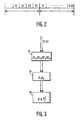
- FIG.1a block diagram of a MCM receiver is shown.
- Analog Digital Converter (11)samples the incoming analog signal at intervals of T seconds.
- Null Detect block (12)detects the null symbol as shown in FIG.2.
- the digitized signalalso enters block (13) in which a Hilbert transform filter converts the received real signal to a complex form.
- the signalthen enters block (14) which uses the output of Null Detect (12) as a rough indicator of the first symbol of each block of data.
- Remove Guard block (14)removes the guard interval preceding each symbol.
- the timing synchronization information ⁇ T/Tis input to Timing Control block (16) and the frequency offset ⁇ is input to Frequency Control block (18).
- These control blockscan be implemented with standard components, such as a phase-locked loop.
- the received signalis adjusted to compensate for any frequency offset based on the estimate received from block (15).
- Analog-Digital Converter (11)has been corrected for ⁇ T/T and any frequency offset of the sampled signal, has been compensated.
- the receivernow takes the FFT of the synchronized and compensated signal in block (20).
- Symbol Synchronizer and Channel Estimator (21)tap symbols S3 and S4 from the output of FFT block (20) and determine the start of each symbol interval and also estimate the frequency response of each carrier, i.e., H k .
- the symbol synchronizationis input to Remove Guard block (14) to be used together with the information from Null Detect block (12) to determine the start of the first symbol of the next symbol interval.
- the estimated frequency response H kis input to Equalizer (22) which determines the maximum likelihood representation of each data symbol at their respective carrier frequencies.
- the transmitter receiver system of the present inventionin which frequency offset compensation and timing synchronization occurs simultaneously and prior to the FFT operation of a receiver, involves a specific data structure which includes at least two (2) single tone symbols which precede the symbols corresponding to the information sought to be transmitted.
- a specific data structurewhich includes at least two (2) single tone symbols which precede the symbols corresponding to the information sought to be transmitted.
- FIG.2one preferred data structure as used in the present invention, is shown comprising a preamble, composed of five symbols, followed by a sequence of data symbols, i.e. the information sought to be transmitted.
- the first symbolis a null symbol, used to obtain a coarse estimate of the start of each symbol interval.
- a simple energy detectordetects a sudden increase in energy from the null symbol to S1 thereby roughly indicating the first symbol of each block of data.
- S1 and S2Following the null symbol are single tone symbols S1 and S2 with different frequencies, transmitted over consecutive data intervals of length NT, and separated by a guard interval of length N g T.
- the frequencies of S1 and S2can be expressed as M 1 / NT and M 2 / NT, respectively. As shown below, M 1 and M 2 should have relatively small values, whose difference is large.
- S1 and S2are then followed by symbols S3 and S4 which contain all the carrier frequencies of the data symbols and are used for symbol synchronization. Finally, S3 and S4 are followed by the symbols corresponding to the desired information.
- the frequency offset and timing mismatchcan be determined prior to performing an FFT over the received symbols, since these symbols do not require any demodulation.
- the mechanics of estimating the frequency offset and timing mismatch using S1 and S2proceeds as follows:.
- H' kH k e j 2 ⁇ (k + ⁇ ) / NT
- H' kH k e j 2 ⁇ (k + ⁇ ) / NT
- Estimator (15)begins in block (31) by dividing the samples of each symbol interval, in half, and forms the following sample vectors from the samples of S1 and S2. Note that although S1 and S2 are consecutive symbols, each of length NT, due to the guard interval of length N g T between these two symbols, S2 is first sampled at time (N+N g )T.
- ⁇ T / Tcan be estimated from the estimates of ⁇ 1 and ⁇ 2 .
- the range of e that can be estimated by this procedurecan be increased by shortening the length of each of the vectors used in the estimation procedure. For small ⁇ T/T and a vector length of N /2, the range over which ⁇ can be estimated unambiguously is
- the mathematical operations involved in arriving at these estimatescan be implemented with specific physical components, such as multipliers, adders, and a readable memory for storage of a lookup table, or they can be implemented through a general purpose or dedicated microprocessor executing software instructions.
- Cramer-Rao lower boundis a measure of the variance of the best estimator for any problem. Indeed, these expressions can be used as exact variances instead of lower bounds, since the maximum likelihood estimate satisfies the Cramer-Rao lower bound.
- J.M. MendelLessons in Digital Estimation Theory, (1987), hereby incorporated by reference as if fully set forth herein.
- Equations (26) and (27)show that lower variance of frequency offset ⁇ and timing mismatch ⁇ T/T is obtained by using values of M 1 and M 2 which are widely spaced.
- M 1 and M 2'should each be relatively small.
- One skilled in the artwill be able to readily experiment with and ascertain highly efficient values of M 1 and M 2 , in order to minimize the variance of the estimates.
- Other factors, such as distortion due to frequency band edges and known interferers at certain frequencieswill also influence the optimum choice of M 1 and M 2 .
Landscapes
- Engineering & Computer Science (AREA)
- Signal Processing (AREA)
- Computer Networks & Wireless Communication (AREA)
- Synchronisation In Digital Transmission Systems (AREA)
- Digital Transmission Methods That Use Modulated Carrier Waves (AREA)
Description


The signal component can be expressed as


These sequences are input to Frequency Offset and Timing Estimator block (15). As shown inFIG. 3, Estimator (15) begins in block (31) by dividing the samples of each symbol interval, inhalf, and forms the following sample vectors from the samples of S1 and S2.


Claims (8)
- A transmission system for transmitting and receiving multicarrier modulateddigital signals, comprising:a transmitter for transmitting data as a multicarrier modulated signal, saidtransmitter including means for transmitting at least a plurality of single tone signals toprecede said multicarrier modulated data signal, said multicarrier modulated data signal andsaid preceding single tone signals comprising a data structure; anda receiver for receiving said data structure, said receiver including means (11)for retrieving said plurality of single tone signals, means (15) for estimating a frequencyoffset and a timing mismatch of said receiver, means (18, 16) for adjusting said receiver tocompensate for said estimated frequency offset and timing mismatch, an FFT block (20) forperforming an FFT operation on the modulated signals, and multiplier means (19) coupledbetween said means (11) and said FFT block (20) to compensate for the frequency offsetbased on the estimate received from said means (15), whereby the estimating means (15) arecoupled between said retrieving means (11) and said multiplier means (19),characterised inthat said means (18, 16) are arranged for compensating for said estimated frequency offsetand timing mismatch only prior to performing the FFT operation by the block (20).
- A transmission system according to claim 1, wherein said plurality of distinctsingle tone signals consist of two distinct single tone signals.
- A transmission system according to claim 2, wherein said data structurecomprises a null symbol, said two distinct single tone signals, and said multicarriermodulated data signals.
- A transmission system according to claim 3, wherein said data structurecomprises a null symbol, said two distinct single tone signals, one or more multicarriermodulated signals for use in symbol synchronization of said receiver, and said multicarriermodulated data signals.
- A receiver for application in the transmission system according to one of theclaims 1-4, the transmission system comprising:a transmitter for transmitting data as a multicarrier modulated signal, saidtransmitter including means for transmitting at least a plurality of single tone signals toprecede said multicarrier modulated data signal, said multicarrier modulated data signal andsaid preceding single tone signals comprising a data structure; anda receiver for receiving said data structure, said receiver including means (11)for retrieving said plurality of single tone signals, means (15) for estimating a frequencyoffset and a timing mismatch of said receiver, means (18, 16) for adjusting said receiver tocompensate for said estimated frequency offset and timing mismatch, an FFT block (20) forperforming an FFT operation on the modulated signals, and multiplier means (19) coupledbetween said means (11) and said FFT block (20) to compensate for the frequency offsetbased on the estimate received from said means (15), whereby the estimating means (15) arecoupled between said retrieving means (11) and said multiplier means (19),characterised inthat said means (18, 16) are arranged for compensating for said estimated frequency offsetand timing mismatch only prior to performing the FFT operation by the block (20).
- A receiver according to claim 5 wherein said plurality of distinct single tonesignals consist of a first single tone signal and a second single tone signal.
- A receiver according to claim 6 wherein a sampler (11) is arranged fordetecting N samples of each of said distinct single tone signals over a symbol interval, eachof said single tone signals having a frequency equal to an even multiple of the inverse of saidsymbol interval, and wherein said frequency offset and timing mismatch estimator (15)comprises means (31) for dividing each of said distinct single tone signals into a first andsecond sample vector, for a total of four sample vectors, each of said first sample vectorscomprising a first part of said samples of said single tone signal, respectively, and each ofsaid second sample vectors comprising a second part of said samples of said single tonesignal, respectively; means (32) for computing a first inverse tangent of the ratio of animaginary part to a real part of the product of the transform of said second sample vector ofsaid first single tone signal and said first sample vector of said first single tone signal, andmeans (32) for computing a second inverse tangent of the ratio of an imaginary part to a realpart of the product of the transform of said second sample vector of said second single tonesignal and said first sample vector of said second single tone signal; means (33) for computing said estimated frequency offset as the ratio of the difference between the productof said first inverse tangent and said second multiple and the product of said second inversetangent to said multiple, to the sum of the product of π and the difference between said firstand second multiples and the difference between said first and second inverse tangents; andmeans (33) for computing said estimated timing mismatch as the ratio of the differencebetween said first and second inverse tangents, to the product of π and the difference betweensaid first and second multiples.
- A receiver according to claim 7 wherein said first part of samples and saidsecond part of samples, for each of said single tone signals comprise disjoint sets of samples.
Applications Claiming Priority (3)
| Application Number | Priority Date | Filing Date | Title |
|---|---|---|---|
| US605318 | 1996-02-08 | ||
| US08/605,318US5802117A (en) | 1996-02-08 | 1996-02-08 | Method and apparatus for joint frequency offset and timing estimation of a multicarrier modulation system |
| PCT/IB1997/000041WO1997029568A1 (en) | 1996-02-08 | 1997-01-22 | Method and apparatus for joint frequency offset and timing estimation of a multicarrier modulation system |
Publications (2)
| Publication Number | Publication Date |
|---|---|
| EP0827655A1 EP0827655A1 (en) | 1998-03-11 |
| EP0827655B1true EP0827655B1 (en) | 2004-08-18 |
Family
ID=24423162
Family Applications (1)
| Application Number | Title | Priority Date | Filing Date |
|---|---|---|---|
| EP97900090AExpired - LifetimeEP0827655B1 (en) | 1996-02-08 | 1997-01-22 | Method and apparatus for joint frequency offset and timing estimation of a multicarrier modulation system |
Country Status (6)
| Country | Link |
|---|---|
| US (1) | US5802117A (en) |
| EP (1) | EP0827655B1 (en) |
| JP (1) | JPH11503895A (en) |
| KR (1) | KR19980703715A (en) |
| DE (1) | DE69730283T2 (en) |
| WO (1) | WO1997029568A1 (en) |
Families Citing this family (80)
| Publication number | Priority date | Publication date | Assignee | Title |
|---|---|---|---|---|
| US6334219B1 (en) | 1994-09-26 | 2001-12-25 | Adc Telecommunications Inc. | Channel selection for a hybrid fiber coax network |
| US7280564B1 (en) | 1995-02-06 | 2007-10-09 | Adc Telecommunications, Inc. | Synchronization techniques in multipoint-to-point communication using orthgonal frequency division multiplexing |
| USRE42236E1 (en) | 1995-02-06 | 2011-03-22 | Adc Telecommunications, Inc. | Multiuse subcarriers in multipoint-to-point communication using orthogonal frequency division multiplexing |
| CA2183140C (en)* | 1996-08-12 | 2001-11-20 | Grant Mcgibney | Ofdm timing and frequency recovery system |
| FI102231B (en)* | 1996-09-16 | 1998-10-30 | Nokia Technology Gmbh | Method for adjusting symbol synchronization and sampling rate in a device receiving OFDM modulated transmissions and a device implementing the method |
| IL120210A (en)* | 1997-02-13 | 1999-12-31 | Dspc Tech Ltd | Synchronization system and method for digital communication systems |
| TW465234B (en)* | 1997-02-18 | 2001-11-21 | Discovision Ass | Single chip VLSI implementation of a digital receiver employing orthogonal frequency division multiplexing |
| US6633550B1 (en) | 1997-02-20 | 2003-10-14 | Telefonaktiebolaget Lm Ericsson (Publ) | Radio transceiver on a chip |
| SE9703630L (en)* | 1997-03-03 | 1998-09-04 | Telia Ab | Improvements to, or with respect to, synchronization |
| JPH10257013A (en)* | 1997-03-14 | 1998-09-25 | Toshiba Corp | Receiver |
| JPH10313286A (en)* | 1997-05-13 | 1998-11-24 | Sony Corp | Receiver |
| US6134286A (en)* | 1997-10-14 | 2000-10-17 | Ericsson Inc. | Synchronization techniques and systems for radiocommunication |
| US6359878B1 (en) | 1998-07-20 | 2002-03-19 | Wirless Facilities, Inc. | Non-data-aided maximum likelihood based feedforward timing synchronization method |
| US6493397B1 (en)* | 1997-10-20 | 2002-12-10 | Matsushita Electric Industrial Co. Ltd. | Radio communication device and radio communication method |
| US6654432B1 (en) | 1998-06-08 | 2003-11-25 | Wireless Facilities, Inc. | Joint maximum likelihood frame and timing estimation for a digital receiver |
| US6061574A (en)* | 1997-10-28 | 2000-05-09 | Motorola, Inc. | Method and apparatus in a wireless communication system for reducing errors caused by intersymbol interference during a simulcast transmission |
| KR100263372B1 (en)* | 1997-11-29 | 2000-08-01 | 전주범 | Simple Frequency Acquisition Method and Device Thereof in Orthogonal Division Band System |
| JP3981898B2 (en)* | 1998-02-20 | 2007-09-26 | ソニー株式会社 | Signal receiving apparatus and method, and recording medium |
| US6950444B1 (en)* | 1999-08-24 | 2005-09-27 | Paradyne Corporation | System and method for a robust preamble and transmission delimiting in a switched-carrier transceiver |
| DE19814530A1 (en)* | 1998-04-01 | 1999-10-07 | Bosch Gmbh Robert | Method for the digital transmission of data in a wireless communication network and receiving device for receiving data transmitted according to the method |
| SE9801748L (en)* | 1998-05-18 | 1999-11-19 | Telia Ab | Improvements in or relating to telecommunication transmission systems |
| KR100293615B1 (en)* | 1998-09-07 | 2002-05-01 | 김춘호 | Carrier Frequency Offset Estimation Method Using Reference Symbol Composed of Repetitive Signals in OPM System |
| US6442221B1 (en)* | 1998-09-22 | 2002-08-27 | Zenith Electronics Corporation | Ghost eliminating equalizer |
| US6310926B1 (en)* | 1998-09-25 | 2001-10-30 | Telefonaktiebolaget Lm Ericsson (Publ) | Adjustment of the sampling frequency in a multicarrier receiver |
| GB9823812D0 (en)* | 1998-10-30 | 1998-12-23 | Mitsubishi Electric Inf Tech | Multicarrier communications systems |
| US6430235B1 (en) | 1998-11-05 | 2002-08-06 | Wireless Facilities, Inc. | Non-data-aided feedforward timing synchronization method |
| DE19854167C2 (en)* | 1998-11-24 | 2000-09-28 | Siemens Ag | Frequency-stabilized transmission / reception circuit |
| US6111919A (en)* | 1999-01-20 | 2000-08-29 | Intellon Corporation | Synchronization of OFDM signals |
| EP1028564B1 (en) | 1999-02-11 | 2010-04-07 | Motorola, Inc. | Estimation of carrier and sampling frequency offsets in multicarrier receivers |
| US6760300B1 (en) | 1999-02-17 | 2004-07-06 | Imec | High speed wireless OFDM transceiver modem |
| EP1030489A1 (en)* | 1999-02-17 | 2000-08-23 | Interuniversitair Micro-Elektronica Centrum Vzw | Multicarrier transceiver |
| EP1083721A1 (en)* | 1999-09-09 | 2001-03-14 | Interuniversitair Micro-Elektronica Centrum Vzw | Multicarrier transceiver |
| EP1039713B1 (en)* | 1999-03-26 | 2006-05-31 | Nec Corporation | Reduction of delay in multicarrier receivers |
| US6549587B1 (en)* | 1999-09-20 | 2003-04-15 | Broadcom Corporation | Voice and data exchange over a packet based network with timing recovery |
| US6269132B1 (en) | 1999-04-26 | 2001-07-31 | Intellon Corporation | Windowing function for maintaining orthogonality of channels in the reception of OFDM symbols |
| US6074086A (en)* | 1999-04-26 | 2000-06-13 | Intellon Corporation | Synchronization of OFDM signals with improved windowing |
| US6546056B1 (en)* | 1999-05-28 | 2003-04-08 | 3Com Corporation | Timing recovery in a multi-tone modem |
| US6693983B1 (en)* | 1999-10-05 | 2004-02-17 | Her Majesty The Queen In Right Of Canada, As Represented By The Minister Of Industry Through The Communication Research Centre | Method and system for detection of short digital radio messages |
| US6477210B2 (en)* | 2000-02-07 | 2002-11-05 | At&T Corp. | System for near optimal joint channel estimation and data detection for COFDM systems |
| JP2003524338A (en)* | 2000-02-22 | 2003-08-12 | コーニンクレッカ フィリップス エレクトロニクス エヌ ヴィ | Multi-channel receiver with channel estimator |
| US6956814B1 (en)* | 2000-02-29 | 2005-10-18 | Worldspace Corporation | Method and apparatus for mobile platform reception and synchronization in direct digital satellite broadcast system |
| US7010062B2 (en)* | 2000-04-04 | 2006-03-07 | Broadcom Corporation | System and method for multi-carrier modulation |
| JP2001339328A (en)* | 2000-05-25 | 2001-12-07 | Communication Research Laboratory | Receiver, reception method, and information recording medium |
| DE10026538A1 (en)* | 2000-05-27 | 2001-11-29 | Deutsche Telekom Ag | Method and diversity receiving device for receiving a multicarrier signal |
| DE10039902B4 (en)* | 2000-08-16 | 2011-04-28 | Rohde & Schwarz Gmbh & Co. Kg | Method for frequency and time synchronization of a receiver |
| US20020065047A1 (en)* | 2000-11-30 | 2002-05-30 | Moose Paul H. | Synchronization, channel estimation and pilot tone tracking system |
| US7012881B2 (en)* | 2000-12-29 | 2006-03-14 | Samsung Electronic Co., Ltd. | Timing and frequency offset estimation scheme for OFDM systems by using an analytic tone |
| JP4164363B2 (en)* | 2001-02-22 | 2008-10-15 | コーニンクレッカ フィリップス エレクトロニクス エヌ ヴィ | Reduced complexity intercarrier interference cancellation |
| EP1364506A2 (en)* | 2001-02-22 | 2003-11-26 | Koninklijke Philips Electronics N.V. | Multicarrier transmission system with reduced complexity channel response estimation |
| EP1364507A2 (en)* | 2001-02-22 | 2003-11-26 | Koninklijke Philips Electronics N.V. | Multicarrier transmission system with reduced complexity leakage matrix multiplication |
| US7035358B1 (en)* | 2001-02-23 | 2006-04-25 | Arraycomm, Inc. | Method and apparatus for receiving a wideband signal in the presence of multipath channel imperfections and frequency offset |
| US8619922B1 (en) | 2002-02-04 | 2013-12-31 | Marvell International Ltd. | Method and apparatus for acquisition and tracking of orthogonal frequency division multiplexing symbol timing, carrier frequency offset and phase noise |
| US7218691B1 (en) | 2001-03-05 | 2007-05-15 | Marvell International Ltd. | Method and apparatus for estimation of orthogonal frequency division multiplexing symbol timing and carrier frequency offset |
| EP1267536A1 (en)* | 2001-06-13 | 2002-12-18 | Conexant Systems, Inc. | Multicarrier receiver with detection of the transmission mode and length of the guard interval |
| US7962162B2 (en)* | 2001-08-07 | 2011-06-14 | At&T Intellectual Property Ii, L.P. | Simulcasting OFDM system having mobile station location identification |
| KR100438519B1 (en)* | 2001-12-28 | 2004-07-03 | 한국전자통신연구원 | Receiving system for estimating a symbol timing forward structure and timing estimating method therefor |
| JP2003319005A (en)* | 2002-02-20 | 2003-11-07 | Mitsubishi Electric Corp | Symbol timing correction circuit, receiver, symbol timing correction method, and demodulation processing method |
| US7245672B2 (en)* | 2002-06-27 | 2007-07-17 | Telefonaktiebolaget Lm Ericsson (Publ) | Method and apparatus for phase-domain semi-coherent demodulation |
| US7277504B2 (en)* | 2002-06-27 | 2007-10-02 | Telefonktiebolaget Lm Ericsson (Publ) | Method and system for concurrent estimation of frequency offset and modulation index |
| KR100489409B1 (en)* | 2002-10-26 | 2005-05-16 | 텔레시스 인코포레이티드 | Method for improving a performance of transmitter and receiver in wireless communication systems |
| KR100488802B1 (en)* | 2002-12-09 | 2005-05-12 | 한국전자통신연구원 | Method and apparatus for carrier frequency offset and sampling clock frequency offset tracking in orthogonal frequency division multiplexing wireless communication systems |
| US7385617B2 (en)* | 2003-05-07 | 2008-06-10 | Illinois Institute Of Technology | Methods for multi-user broadband wireless channel estimation |
| US7145970B2 (en)* | 2003-07-07 | 2006-12-05 | Beno Corporation | Frequency offset detector for AFC under rayleigh fading |
| KR100555508B1 (en)* | 2003-07-22 | 2006-03-03 | 삼성전자주식회사 | Impulse Noise Suppression Circuit and Method in Orthogonal Frequency Division Multiplexing System |
| US8724447B2 (en) | 2004-01-28 | 2014-05-13 | Qualcomm Incorporated | Timing estimation in an OFDM receiver |
| RU2335853C2 (en)* | 2004-01-28 | 2008-10-10 | Квэлкомм Инкорпорейтед | Timing assessment in ofdm receiver |
| US8433005B2 (en) | 2004-01-28 | 2013-04-30 | Qualcomm Incorporated | Frame synchronization and initial symbol timing acquisition system and method |
| KR100770924B1 (en)* | 2005-02-04 | 2007-10-26 | 삼성전자주식회사 | Frequency Error Compensation Device and Method in Wireless Communication System |
| KR100717847B1 (en) | 2005-12-09 | 2007-05-14 | 한국전자통신연구원 | Method and apparatus for frequency offset estimation and compensation in multiband OFMD ultra wideband system using time frequency hopping |
| US7660339B2 (en)* | 2005-12-09 | 2010-02-09 | Electronics And Telecommunications Research Institute | Apparatus and method for estimating and correcting frequency offset in MB-OFDM UWB system using time frequency hopping |
| US20070177492A1 (en)* | 2006-01-27 | 2007-08-02 | Qualcomm Incorporated | Methods and tools for expanding coverage of an ofdm broadcast transmitter via transmit timing advance |
| RU2411680C2 (en)* | 2006-01-27 | 2011-02-10 | Квэлкомм Инкорпорейтед | Methods and tools to expand coverage of ofdm system broadcasting transmitter through shift with anticipation of transfer synchronisation |
| US8379739B2 (en)* | 2008-03-10 | 2013-02-19 | St Ericsson Sa | Method and system for impact mitigation of sudden carrier frequency shifts in OFDM receivers |
| CN101562595B (en)* | 2009-05-25 | 2012-10-24 | 北京天碁科技有限公司 | Method and device for jointly estimating frequency deviation and symbol timing deviation |
| US8576743B2 (en)* | 2010-12-28 | 2013-11-05 | Qualcomm Incorporated | Apparatus and methods for estimating an unknown frequency error of a tone signal |
| US10257004B2 (en) | 2014-12-23 | 2019-04-09 | Telefonaktiebolaget Lm Ericsson (Publ) | Inter-block interference suppression using a null guard interval |
| US10334533B2 (en) | 2016-11-02 | 2019-06-25 | At&T Intellectual Property I, L.P. | Non-orthogonal design for channel state information reference signals for a 5G air interface or other next generation network interfaces |
| US10237032B2 (en) | 2017-01-06 | 2019-03-19 | At&T Intellectual Property I, L.P. | Adaptive channel state information reference signal configurations for a 5G wireless communication network or other next generation network |
| US10320512B2 (en)* | 2017-01-08 | 2019-06-11 | At&T Intellectual Property I, L.P. | Interference cancelation for 5G or other next generation network |
| CN107888526A (en)* | 2017-12-27 | 2018-04-06 | 天津赛特凯特科技发展有限公司 | A kind of set top box channel filtering and carrier recovery circuit |
Family Cites Families (7)
| Publication number | Priority date | Publication date | Assignee | Title |
|---|---|---|---|---|
| US5029184A (en)* | 1990-01-24 | 1991-07-02 | Harris Corporation | Low probability of intercept communication system |
| US5228062A (en)* | 1990-04-16 | 1993-07-13 | Telebit Corporation | Method and apparatus for correcting for clock and carrier frequency offset, and phase jitter in multicarrier modems |
| US5225062A (en)* | 1991-02-27 | 1993-07-06 | W. R. Grace & Co. -Conn. | Electrophoretic gel for separation and recovery of substances and its use |
| SE9400116L (en)* | 1994-01-18 | 1995-03-27 | Telia Ab | Procedure and arrangement for synchronization in OFDM modulation |
| US5608784A (en)* | 1994-01-24 | 1997-03-04 | Miller; Joel F. | Method of personnel verification using voice recognition |
| JP2989742B2 (en)* | 1994-05-20 | 1999-12-13 | 株式会社日立製作所 | Digital broadcasting system, transmission system for the digital broadcasting, and receiving system for the digital broadcasting |
| JP3421880B2 (en)* | 1994-10-05 | 2003-06-30 | ソニー株式会社 | Demodulator |
- 1996
- 1996-02-08USUS08/605,318patent/US5802117A/ennot_activeExpired - Fee Related
- 1997
- 1997-01-22WOPCT/IB1997/000041patent/WO1997029568A1/ennot_activeApplication Discontinuation
- 1997-01-22EPEP97900090Apatent/EP0827655B1/ennot_activeExpired - Lifetime
- 1997-01-22DEDE69730283Tpatent/DE69730283T2/ennot_activeExpired - Fee Related
- 1997-01-22KRKR1019970707115Apatent/KR19980703715A/ennot_activeAbandoned
- 1997-01-22JPJP9528327Apatent/JPH11503895A/ennot_activeWithdrawn
Also Published As
| Publication number | Publication date |
|---|---|
| KR19980703715A (en) | 1998-12-05 |
| DE69730283D1 (en) | 2004-09-23 |
| EP0827655A1 (en) | 1998-03-11 |
| US5802117A (en) | 1998-09-01 |
| JPH11503895A (en) | 1999-03-30 |
| DE69730283T2 (en) | 2005-08-25 |
| WO1997029568A1 (en) | 1997-08-14 |
Similar Documents
| Publication | Publication Date | Title |
|---|---|---|
| EP0827655B1 (en) | Method and apparatus for joint frequency offset and timing estimation of a multicarrier modulation system | |
| JP4721530B2 (en) | Method and OFDM receiver for correcting frequency of local oscillator in orthogonal frequency division multiplexing system | |
| US7039000B2 (en) | Timing synchronization for OFDM-based wireless networks | |
| EP0998068B1 (en) | Ofdm (orthogonal frequency division multiplexing) receiver | |
| US7843805B2 (en) | Method and circuit for frequency offset estimation in frequency domain in the orthogonal frequency division multiplexing baseband receiver for IEEE 802.11a/g wireless LAN standard | |
| KR100377257B1 (en) | Method and apparatus for fine frequency synchronization in multi-carrier demodulation systems | |
| US7664189B2 (en) | OFDM demodulator, receiver, and method | |
| US7133479B2 (en) | Frequency synchronization apparatus and method for OFDM systems | |
| US7627059B2 (en) | Method of robust timing detection and carrier frequency offset estimation for OFDM systems | |
| US6584164B1 (en) | Method for forming a training sequence | |
| US7099397B2 (en) | Receiver of an orthogonal frequency division multiplexing system | |
| US20020065047A1 (en) | Synchronization, channel estimation and pilot tone tracking system | |
| EP1195961A2 (en) | Frequency offset correction in multicarrier receivers | |
| EP0920163A2 (en) | Estimating of coarse frequency offset in multicarrier receivers | |
| US6459745B1 (en) | Frequency/timing recovery circuit for orthogonal frequency division multiplexed signals | |
| CN101375569B (en) | Method and system for estimating symbol time error in broadband transmission system | |
| JP2005312027A (en) | Receiver | |
| KR20070011114A (en) | Orthogonal Frequency Division Multiple Demodulation Apparatus and Method | |
| US20080123757A1 (en) | Apparatus and Method For Receiving an Orthogonal Frequency Division Multiplexed Signal | |
| EP1193934A2 (en) | Frequency offset correction in multicarrier receivers | |
| AU749787B2 (en) | Coarse frequency synchronization in multicarrier systems systems | |
| EP0895388B1 (en) | Symbol synchronisation and mode detection for multicarrier signals | |
| WO2001069878A1 (en) | Method of selecting a position of a fft window in a cofdm receiver | |
| EP1274209A1 (en) | Frequency correction for a multicarrier system | |
| KR100664018B1 (en) | Synchronous Detection Device for Orthogonal Frequency Division Multiplexing Receiver |
Legal Events
| Date | Code | Title | Description |
|---|---|---|---|
| PUAI | Public reference made under article 153(3) epc to a published international application that has entered the european phase | Free format text:ORIGINAL CODE: 0009012 | |
| AK | Designated contracting states | Kind code of ref document:A1 Designated state(s):DE FR GB | |
| 17P | Request for examination filed | Effective date:19980216 | |
| RAP3 | Party data changed (applicant data changed or rights of an application transferred) | Owner name:KONINKLIJKE PHILIPS ELECTRONICS N.V. | |
| 17Q | First examination report despatched | Effective date:20030709 | |
| GRAP | Despatch of communication of intention to grant a patent | Free format text:ORIGINAL CODE: EPIDOSNIGR1 | |
| GRAS | Grant fee paid | Free format text:ORIGINAL CODE: EPIDOSNIGR3 | |
| GRAA | (expected) grant | Free format text:ORIGINAL CODE: 0009210 | |
| AK | Designated contracting states | Kind code of ref document:B1 Designated state(s):DE FR GB | |
| REG | Reference to a national code | Ref country code:GB Ref legal event code:FG4D | |
| REF | Corresponds to: | Ref document number:69730283 Country of ref document:DE Date of ref document:20040923 Kind code of ref document:P | |
| PGFP | Annual fee paid to national office [announced via postgrant information from national office to epo] | Ref country code:GB Payment date:20050127 Year of fee payment:9 Ref country code:FR Payment date:20050127 Year of fee payment:9 | |
| PGFP | Annual fee paid to national office [announced via postgrant information from national office to epo] | Ref country code:DE Payment date:20050315 Year of fee payment:9 | |
| PLBE | No opposition filed within time limit | Free format text:ORIGINAL CODE: 0009261 | |
| STAA | Information on the status of an ep patent application or granted ep patent | Free format text:STATUS: NO OPPOSITION FILED WITHIN TIME LIMIT | |
| REG | Reference to a national code | Ref country code:GB Ref legal event code:746 Effective date:20050628 | |
| ET | Fr: translation filed | ||
| 26N | No opposition filed | Effective date:20050519 | |
| PG25 | Lapsed in a contracting state [announced via postgrant information from national office to epo] | Ref country code:GB Free format text:LAPSE BECAUSE OF NON-PAYMENT OF DUE FEES Effective date:20060122 | |
| PG25 | Lapsed in a contracting state [announced via postgrant information from national office to epo] | Ref country code:FR Free format text:LAPSE BECAUSE OF NON-PAYMENT OF DUE FEES Effective date:20060131 | |
| PG25 | Lapsed in a contracting state [announced via postgrant information from national office to epo] | Ref country code:DE Free format text:LAPSE BECAUSE OF NON-PAYMENT OF DUE FEES Effective date:20060801 | |
| GBPC | Gb: european patent ceased through non-payment of renewal fee | Effective date:20060122 | |
| REG | Reference to a national code | Ref country code:FR Ref legal event code:ST Effective date:20060929 |