EP0827203A2 - Clock skew minimisation system and method for integrated circuits - Google Patents
Clock skew minimisation system and method for integrated circuitsDownload PDFInfo
- Publication number
- EP0827203A2 EP0827203A2EP97305479AEP97305479AEP0827203A2EP 0827203 A2EP0827203 A2EP 0827203A2EP 97305479 AEP97305479 AEP 97305479AEP 97305479 AEP97305479 AEP 97305479AEP 0827203 A2EP0827203 A2EP 0827203A2
- Authority
- EP
- European Patent Office
- Prior art keywords
- chip
- primary
- clock
- face
- substrate
- Prior art date
- Legal status (The legal status is an assumption and is not a legal conclusion. Google has not performed a legal analysis and makes no representation as to the accuracy of the status listed.)
- Granted
Links
Images


Classifications
- H—ELECTRICITY
- H01—ELECTRIC ELEMENTS
- H01L—SEMICONDUCTOR DEVICES NOT COVERED BY CLASS H10
- H01L24/00—Arrangements for connecting or disconnecting semiconductor or solid-state bodies; Methods or apparatus related thereto
- H01L24/73—Means for bonding being of different types provided for in two or more of groups H01L24/10, H01L24/18, H01L24/26, H01L24/34, H01L24/42, H01L24/50, H01L24/63, H01L24/71
- H—ELECTRICITY
- H01—ELECTRIC ELEMENTS
- H01L—SEMICONDUCTOR DEVICES NOT COVERED BY CLASS H10
- H01L23/00—Details of semiconductor or other solid state devices
- H01L23/48—Arrangements for conducting electric current to or from the solid state body in operation, e.g. leads, terminal arrangements ; Selection of materials therefor
- H01L23/50—Arrangements for conducting electric current to or from the solid state body in operation, e.g. leads, terminal arrangements ; Selection of materials therefor for integrated circuit devices, e.g. power bus, number of leads
- H—ELECTRICITY
- H01—ELECTRIC ELEMENTS
- H01L—SEMICONDUCTOR DEVICES NOT COVERED BY CLASS H10
- H01L25/00—Assemblies consisting of a plurality of semiconductor or other solid state devices
- H01L25/03—Assemblies consisting of a plurality of semiconductor or other solid state devices all the devices being of a type provided for in a single subclass of subclasses H10B, H10D, H10F, H10H, H10K or H10N, e.g. assemblies of rectifier diodes
- H01L25/04—Assemblies consisting of a plurality of semiconductor or other solid state devices all the devices being of a type provided for in a single subclass of subclasses H10B, H10D, H10F, H10H, H10K or H10N, e.g. assemblies of rectifier diodes the devices not having separate containers
- H01L25/065—Assemblies consisting of a plurality of semiconductor or other solid state devices all the devices being of a type provided for in a single subclass of subclasses H10B, H10D, H10F, H10H, H10K or H10N, e.g. assemblies of rectifier diodes the devices not having separate containers the devices being of a type provided for in group H10D89/00
- H01L25/0657—Stacked arrangements of devices
- H—ELECTRICITY
- H10—SEMICONDUCTOR DEVICES; ELECTRIC SOLID-STATE DEVICES NOT OTHERWISE PROVIDED FOR
- H10D—INORGANIC ELECTRIC SEMICONDUCTOR DEVICES
- H10D89/00—Aspects of integrated devices not covered by groups H10D84/00 - H10D88/00
- H10D89/10—Integrated device layouts
- H—ELECTRICITY
- H01—ELECTRIC ELEMENTS
- H01L—SEMICONDUCTOR DEVICES NOT COVERED BY CLASS H10
- H01L2224/00—Indexing scheme for arrangements for connecting or disconnecting semiconductor or solid-state bodies and methods related thereto as covered by H01L24/00
- H01L2224/01—Means for bonding being attached to, or being formed on, the surface to be connected, e.g. chip-to-package, die-attach, "first-level" interconnects; Manufacturing methods related thereto
- H01L2224/10—Bump connectors; Manufacturing methods related thereto
- H01L2224/15—Structure, shape, material or disposition of the bump connectors after the connecting process
- H01L2224/16—Structure, shape, material or disposition of the bump connectors after the connecting process of an individual bump connector
- H01L2224/161—Disposition
- H01L2224/16135—Disposition the bump connector connecting between different semiconductor or solid-state bodies, i.e. chip-to-chip
- H01L2224/16145—Disposition the bump connector connecting between different semiconductor or solid-state bodies, i.e. chip-to-chip the bodies being stacked
- H—ELECTRICITY
- H01—ELECTRIC ELEMENTS
- H01L—SEMICONDUCTOR DEVICES NOT COVERED BY CLASS H10
- H01L2224/00—Indexing scheme for arrangements for connecting or disconnecting semiconductor or solid-state bodies and methods related thereto as covered by H01L24/00
- H01L2224/01—Means for bonding being attached to, or being formed on, the surface to be connected, e.g. chip-to-package, die-attach, "first-level" interconnects; Manufacturing methods related thereto
- H01L2224/10—Bump connectors; Manufacturing methods related thereto
- H01L2224/15—Structure, shape, material or disposition of the bump connectors after the connecting process
- H01L2224/16—Structure, shape, material or disposition of the bump connectors after the connecting process of an individual bump connector
- H01L2224/161—Disposition
- H01L2224/16151—Disposition the bump connector connecting between a semiconductor or solid-state body and an item not being a semiconductor or solid-state body, e.g. chip-to-substrate, chip-to-passive
- H01L2224/16221—Disposition the bump connector connecting between a semiconductor or solid-state body and an item not being a semiconductor or solid-state body, e.g. chip-to-substrate, chip-to-passive the body and the item being stacked
- H01L2224/16225—Disposition the bump connector connecting between a semiconductor or solid-state body and an item not being a semiconductor or solid-state body, e.g. chip-to-substrate, chip-to-passive the body and the item being stacked the item being non-metallic, e.g. insulating substrate with or without metallisation
- H01L2224/16227—Disposition the bump connector connecting between a semiconductor or solid-state body and an item not being a semiconductor or solid-state body, e.g. chip-to-substrate, chip-to-passive the body and the item being stacked the item being non-metallic, e.g. insulating substrate with or without metallisation the bump connector connecting to a bond pad of the item
- H—ELECTRICITY
- H01—ELECTRIC ELEMENTS
- H01L—SEMICONDUCTOR DEVICES NOT COVERED BY CLASS H10
- H01L2224/00—Indexing scheme for arrangements for connecting or disconnecting semiconductor or solid-state bodies and methods related thereto as covered by H01L24/00
- H01L2224/01—Means for bonding being attached to, or being formed on, the surface to be connected, e.g. chip-to-package, die-attach, "first-level" interconnects; Manufacturing methods related thereto
- H01L2224/10—Bump connectors; Manufacturing methods related thereto
- H01L2224/15—Structure, shape, material or disposition of the bump connectors after the connecting process
- H01L2224/17—Structure, shape, material or disposition of the bump connectors after the connecting process of a plurality of bump connectors
- H01L2224/1701—Structure
- H01L2224/1703—Bump connectors having different sizes, e.g. different diameters, heights or widths
- H—ELECTRICITY
- H01—ELECTRIC ELEMENTS
- H01L—SEMICONDUCTOR DEVICES NOT COVERED BY CLASS H10
- H01L2224/00—Indexing scheme for arrangements for connecting or disconnecting semiconductor or solid-state bodies and methods related thereto as covered by H01L24/00
- H01L2224/01—Means for bonding being attached to, or being formed on, the surface to be connected, e.g. chip-to-package, die-attach, "first-level" interconnects; Manufacturing methods related thereto
- H01L2224/42—Wire connectors; Manufacturing methods related thereto
- H01L2224/47—Structure, shape, material or disposition of the wire connectors after the connecting process
- H01L2224/48—Structure, shape, material or disposition of the wire connectors after the connecting process of an individual wire connector
- H01L2224/4805—Shape
- H01L2224/4809—Loop shape
- H01L2224/48091—Arched
- H—ELECTRICITY
- H01—ELECTRIC ELEMENTS
- H01L—SEMICONDUCTOR DEVICES NOT COVERED BY CLASS H10
- H01L2224/00—Indexing scheme for arrangements for connecting or disconnecting semiconductor or solid-state bodies and methods related thereto as covered by H01L24/00
- H01L2224/01—Means for bonding being attached to, or being formed on, the surface to be connected, e.g. chip-to-package, die-attach, "first-level" interconnects; Manufacturing methods related thereto
- H01L2224/42—Wire connectors; Manufacturing methods related thereto
- H01L2224/47—Structure, shape, material or disposition of the wire connectors after the connecting process
- H01L2224/48—Structure, shape, material or disposition of the wire connectors after the connecting process of an individual wire connector
- H01L2224/484—Connecting portions
- H01L2224/48463—Connecting portions the connecting portion on the bonding area of the semiconductor or solid-state body being a ball bond
- H—ELECTRICITY
- H01—ELECTRIC ELEMENTS
- H01L—SEMICONDUCTOR DEVICES NOT COVERED BY CLASS H10
- H01L2224/00—Indexing scheme for arrangements for connecting or disconnecting semiconductor or solid-state bodies and methods related thereto as covered by H01L24/00
- H01L2224/73—Means for bonding being of different types provided for in two or more of groups H01L2224/10, H01L2224/18, H01L2224/26, H01L2224/34, H01L2224/42, H01L2224/50, H01L2224/63, H01L2224/71
- H01L2224/732—Location after the connecting process
- H01L2224/73201—Location after the connecting process on the same surface
- H01L2224/73207—Bump and wire connectors
- H—ELECTRICITY
- H01—ELECTRIC ELEMENTS
- H01L—SEMICONDUCTOR DEVICES NOT COVERED BY CLASS H10
- H01L2225/00—Details relating to assemblies covered by the group H01L25/00 but not provided for in its subgroups
- H01L2225/03—All the devices being of a type provided for in the same main group of the same subclass of class H10, e.g. assemblies of rectifier diodes
- H01L2225/04—All the devices being of a type provided for in the same main group of the same subclass of class H10, e.g. assemblies of rectifier diodes the devices not having separate containers
- H01L2225/065—All the devices being of a type provided for in the same main group of the same subclass of class H10
- H01L2225/06503—Stacked arrangements of devices
- H01L2225/0651—Wire or wire-like electrical connections from device to substrate
- H—ELECTRICITY
- H01—ELECTRIC ELEMENTS
- H01L—SEMICONDUCTOR DEVICES NOT COVERED BY CLASS H10
- H01L2225/00—Details relating to assemblies covered by the group H01L25/00 but not provided for in its subgroups
- H01L2225/03—All the devices being of a type provided for in the same main group of the same subclass of class H10, e.g. assemblies of rectifier diodes
- H01L2225/04—All the devices being of a type provided for in the same main group of the same subclass of class H10, e.g. assemblies of rectifier diodes the devices not having separate containers
- H01L2225/065—All the devices being of a type provided for in the same main group of the same subclass of class H10
- H01L2225/06503—Stacked arrangements of devices
- H01L2225/06513—Bump or bump-like direct electrical connections between devices, e.g. flip-chip connection, solder bumps
- H—ELECTRICITY
- H01—ELECTRIC ELEMENTS
- H01L—SEMICONDUCTOR DEVICES NOT COVERED BY CLASS H10
- H01L2225/00—Details relating to assemblies covered by the group H01L25/00 but not provided for in its subgroups
- H01L2225/03—All the devices being of a type provided for in the same main group of the same subclass of class H10, e.g. assemblies of rectifier diodes
- H01L2225/04—All the devices being of a type provided for in the same main group of the same subclass of class H10, e.g. assemblies of rectifier diodes the devices not having separate containers
- H01L2225/065—All the devices being of a type provided for in the same main group of the same subclass of class H10
- H01L2225/06503—Stacked arrangements of devices
- H01L2225/06517—Bump or bump-like direct electrical connections from device to substrate
- H—ELECTRICITY
- H01—ELECTRIC ELEMENTS
- H01L—SEMICONDUCTOR DEVICES NOT COVERED BY CLASS H10
- H01L2225/00—Details relating to assemblies covered by the group H01L25/00 but not provided for in its subgroups
- H01L2225/03—All the devices being of a type provided for in the same main group of the same subclass of class H10, e.g. assemblies of rectifier diodes
- H01L2225/04—All the devices being of a type provided for in the same main group of the same subclass of class H10, e.g. assemblies of rectifier diodes the devices not having separate containers
- H01L2225/065—All the devices being of a type provided for in the same main group of the same subclass of class H10
- H01L2225/06503—Stacked arrangements of devices
- H01L2225/06527—Special adaptation of electrical connections, e.g. rewiring, engineering changes, pressure contacts, layout
- H—ELECTRICITY
- H01—ELECTRIC ELEMENTS
- H01L—SEMICONDUCTOR DEVICES NOT COVERED BY CLASS H10
- H01L2225/00—Details relating to assemblies covered by the group H01L25/00 but not provided for in its subgroups
- H01L2225/03—All the devices being of a type provided for in the same main group of the same subclass of class H10, e.g. assemblies of rectifier diodes
- H01L2225/04—All the devices being of a type provided for in the same main group of the same subclass of class H10, e.g. assemblies of rectifier diodes the devices not having separate containers
- H01L2225/065—All the devices being of a type provided for in the same main group of the same subclass of class H10
- H01L2225/06503—Stacked arrangements of devices
- H01L2225/06555—Geometry of the stack, e.g. form of the devices, geometry to facilitate stacking
- H01L2225/06562—Geometry of the stack, e.g. form of the devices, geometry to facilitate stacking at least one device in the stack being rotated or offset
- H—ELECTRICITY
- H01—ELECTRIC ELEMENTS
- H01L—SEMICONDUCTOR DEVICES NOT COVERED BY CLASS H10
- H01L2924/00—Indexing scheme for arrangements or methods for connecting or disconnecting semiconductor or solid-state bodies as covered by H01L24/00
- H01L2924/01—Chemical elements
- H01L2924/01004—Beryllium [Be]
- H—ELECTRICITY
- H01—ELECTRIC ELEMENTS
- H01L—SEMICONDUCTOR DEVICES NOT COVERED BY CLASS H10
- H01L2924/00—Indexing scheme for arrangements or methods for connecting or disconnecting semiconductor or solid-state bodies as covered by H01L24/00
- H01L2924/01—Chemical elements
- H01L2924/01033—Arsenic [As]
- H—ELECTRICITY
- H01—ELECTRIC ELEMENTS
- H01L—SEMICONDUCTOR DEVICES NOT COVERED BY CLASS H10
- H01L2924/00—Indexing scheme for arrangements or methods for connecting or disconnecting semiconductor or solid-state bodies as covered by H01L24/00
- H01L2924/01—Chemical elements
- H01L2924/01075—Rhenium [Re]
- H—ELECTRICITY
- H01—ELECTRIC ELEMENTS
- H01L—SEMICONDUCTOR DEVICES NOT COVERED BY CLASS H10
- H01L2924/00—Indexing scheme for arrangements or methods for connecting or disconnecting semiconductor or solid-state bodies as covered by H01L24/00
- H01L2924/01—Chemical elements
- H01L2924/01082—Lead [Pb]
- H—ELECTRICITY
- H01—ELECTRIC ELEMENTS
- H01L—SEMICONDUCTOR DEVICES NOT COVERED BY CLASS H10
- H01L2924/00—Indexing scheme for arrangements or methods for connecting or disconnecting semiconductor or solid-state bodies as covered by H01L24/00
- H01L2924/095—Indexing scheme for arrangements or methods for connecting or disconnecting semiconductor or solid-state bodies as covered by H01L24/00 with a principal constituent of the material being a combination of two or more materials provided in the groups H01L2924/013 - H01L2924/0715
- H01L2924/097—Glass-ceramics, e.g. devitrified glass
- H01L2924/09701—Low temperature co-fired ceramic [LTCC]
- H—ELECTRICITY
- H01—ELECTRIC ELEMENTS
- H01L—SEMICONDUCTOR DEVICES NOT COVERED BY CLASS H10
- H01L2924/00—Indexing scheme for arrangements or methods for connecting or disconnecting semiconductor or solid-state bodies as covered by H01L24/00
- H01L2924/10—Details of semiconductor or other solid state devices to be connected
- H01L2924/11—Device type
- H01L2924/14—Integrated circuits
- H—ELECTRICITY
- H01—ELECTRIC ELEMENTS
- H01L—SEMICONDUCTOR DEVICES NOT COVERED BY CLASS H10
- H01L2924/00—Indexing scheme for arrangements or methods for connecting or disconnecting semiconductor or solid-state bodies as covered by H01L24/00
- H01L2924/15—Details of package parts other than the semiconductor or other solid state devices to be connected
- H01L2924/151—Die mounting substrate
- H01L2924/1515—Shape
- H01L2924/15151—Shape the die mounting substrate comprising an aperture, e.g. for underfilling, outgassing, window type wire connections
- H—ELECTRICITY
- H01—ELECTRIC ELEMENTS
- H01L—SEMICONDUCTOR DEVICES NOT COVERED BY CLASS H10
- H01L2924/00—Indexing scheme for arrangements or methods for connecting or disconnecting semiconductor or solid-state bodies as covered by H01L24/00
- H01L2924/15—Details of package parts other than the semiconductor or other solid state devices to be connected
- H01L2924/151—Die mounting substrate
- H01L2924/1515—Shape
- H01L2924/15153—Shape the die mounting substrate comprising a recess for hosting the device
- H—ELECTRICITY
- H01—ELECTRIC ELEMENTS
- H01L—SEMICONDUCTOR DEVICES NOT COVERED BY CLASS H10
- H01L2924/00—Indexing scheme for arrangements or methods for connecting or disconnecting semiconductor or solid-state bodies as covered by H01L24/00
- H01L2924/15—Details of package parts other than the semiconductor or other solid state devices to be connected
- H01L2924/151—Die mounting substrate
- H01L2924/153—Connection portion
- H01L2924/1532—Connection portion the connection portion being formed on the die mounting surface of the substrate
- H—ELECTRICITY
- H01—ELECTRIC ELEMENTS
- H01L—SEMICONDUCTOR DEVICES NOT COVERED BY CLASS H10
- H01L2924/00—Indexing scheme for arrangements or methods for connecting or disconnecting semiconductor or solid-state bodies as covered by H01L24/00
- H01L2924/19—Details of hybrid assemblies other than the semiconductor or other solid state devices to be connected
- H01L2924/191—Disposition
- H01L2924/19101—Disposition of discrete passive components
- H01L2924/19107—Disposition of discrete passive components off-chip wires
- H—ELECTRICITY
- H01—ELECTRIC ELEMENTS
- H01L—SEMICONDUCTOR DEVICES NOT COVERED BY CLASS H10
- H01L2924/00—Indexing scheme for arrangements or methods for connecting or disconnecting semiconductor or solid-state bodies as covered by H01L24/00
- H01L2924/30—Technical effects
- H01L2924/301—Electrical effects
- H01L2924/3011—Impedance
- H—ELECTRICITY
- H01—ELECTRIC ELEMENTS
- H01L—SEMICONDUCTOR DEVICES NOT COVERED BY CLASS H10
- H01L2924/00—Indexing scheme for arrangements or methods for connecting or disconnecting semiconductor or solid-state bodies as covered by H01L24/00
- H01L2924/30—Technical effects
- H01L2924/301—Electrical effects
- H01L2924/3025—Electromagnetic shielding
Definitions
- the inventionrelates to integrated circuit packaging, and in particular to a packaging system and method for minimising clock skew in integrated circuits.
- Flip-Chip technologysometimes called Controlled Collapse Chip Connection (C4) technology
- C4Controlled Collapse Chip Connection
- the technologyinvolves placing solder-balls on a chip's I/O pads, inverting the chip, and soldering it to a substrate having the same pattern of pads so as to effect interconnection between the chip and the substrate.
- An example of a product of this typeis shown schematically in FIG. 1.
- solderball and C4 technologysee R. Tummala and E. Rymaszewski, Microelectronics Packaging Handbook, Von Nostrand Reinhold, 1989; "Solder Ball Connect Technology", IBM J. of Res. and Dev., Vol. 37, No. 5, Sept. 1993, pp. 581-676.
- the substratehas merely been a second-level package (that is, a passive object having wiring levels).
- Such substrateshave been ceramic, glass-ceramic, or even silicon.
- the purpose of the substratehas been merely to provide a wiring means between chips on the substrate.
- a processorcomprises latches (that hold the "state” of the system) and logic that operates on the current state together with extraneous inputs to "compute” the next state of the system.
- the clockaffects all latches exactly simultaneously so that the transition to this new computed state is complete and instantaneous.
- the clockcannot possibly hit every latch at exactly the same time, so not all of the latches switch at exactly the same time.
- the output of a first latchaffects the input to a second latch (either directly, or through logic circuitry), and the instant at which the clock arrives at the second latch relative to the instant at which the clock arrives at the first latch is uncertain by an amount (+/-)X
- the nominal cycle time(worst case delay path in the machine) must be increased by X to allow for the possibility that the second latch will capture data at a time that is X too early.
- nominal cycle timemust be increased by 2X, because the first latch could have captured the relevant data at a time that is X later than assumed. This is one performance impact of clock skew, which is a factor that is added to the nominal cycle time of a processor to account for the uncertainty associated with the arrival of the clock signal to different parts of a processor.
- the clock signalis a primary input to a chip. It is an oscillator pulse.
- a real central processor (“CP") chipthere typically are tens of thousands of latches that are gated by this clock. If the fanout of a typical gate is f, and there are n latches, then there must be log(base f)(n) intermediate stages of drivers between the original clock pulse (the primary input to the chip) and any latch that is gated by that clock. In a real system, there might be as many as ten levels.
- a secondary substrateor chip
- C4 technologyC4 technology
- DRAMdynamic random access memory
- higher-power logice.g., a processor
- two active chipsi.e., both containing active circuitry
- a further aspect of the inventionis the bonding of a dense and complex logic chip that can dissipate a significant amount of power (e.g., a microprocessor) to a sparsely populated active chip that dissipates significantly less power.
- a dense and complex logic chipthat can dissipate a significant amount of power (e.g., a microprocessor) to a sparsely populated active chip that dissipates significantly less power.
- the sparsely-populated secondary chipcan be used: to distribute clock signals in an extremely controlled manner; as a quiet medium for long busses that can be operated at higher speed in the quiet environment than they could on the surface of the primary chip; and, for optional low-power devices of other types (e.g., DRAM). This is useful because it affords higher performance communication and better skew-control at the system level, and it results in a cheaper package.
- FIG. 1shows a primary substrate C4-bonded to a secondary substrate.
- FIG. 2shows a 16mm x 16mm chip partitioned into 256 square tiles, each with an I/O pad in the center.
- FIG. 3shows a clock driving and calibrating circuitry for 256 tiles on a 16mm x 16mm grid.
- FIG. 4shows a symmetrical wiring scheme for a clock network implemented as a binary tree.
- FIG. 5shows a wire on a quiet bus in accordance with the invention.
- FIG. 6shows a first embodiment of a primary and secondary package configured in accordance with the invention.
- FIG. 7shows a second embodiment of a primary and secondary package configured in accordance with the invention.
- FIG. 8shows a primary, secondary and tertiary chip bonded in accordance with the present invention.
- FIG. 9shows a clock trimming circuit, which delays the clock signal by fixed amounts of time.
- the clock-distribution networkis embedded in the processor chip itself.
- the primary substratecan be a microprocessor chip without a clock-distribution network, and a having a clock distribution network provided on a secondary substrate. Note that the circuitry, and therefore the power, associated with the two systems is the same, i.e., this invention does not inherently create power or cooling problems.
- the active area of the secondary substrateis extremely sparse, and the redriving nodes of the clock-tree can be placed ideally.
- the redriving stagesare placed in symmetric locations, and all wire-lengths and loads are identical throughout the tree. As was previously explained, this would not be possible in any real microprocessor chip having a clock-distribution network that is integral to the microprocessor chip.
- the primary substrate which is densely populatede.g., a microprocessor
- the primary substrate which is densely populatedis conceptually divided into a large number of square "tiles" (e.g., 1mm X 1mm or smaller), and a clock I/O pad is placed in the centre of each tile. All latches within the tile are driven by the clock pad in the centre of the tile.
- a configurationis shown on FIG. 2.
- FIG. 2shows a 16mm X 16mm chip that is partitioned into 16 X 16 tiles, where each tile is a 1mm X 1mm square.
- An I/O pad 200is shown in the centre of each tile. This I/O pad is a local clock-input pad, and it drives all latches within its tile. The worst-case Manhattan distance from an I/O pad to a latch is 1mm in this figure.
- the clock inputs to these I/O padsare provided through solder-ball connections to identically positioned I/O pads on the secondary substrate, which contains the clock distribution circuitry for the primary chip logic. Because of the sparsity of the clock-distribution network on the secondary substrate, the simultaneous arrival of a primary clock signal to all driver pads on the secondary substrate, hence to all tiles on the primary substrate, can be guaranteed to within an extremely small tolerance. This would not be possible in existing microprocessors having integral clock-distribution networks.
- clock-trimming and calibrating circuitrycan also be embedded in the clock-distribution network for even better skew control.
- the inventionsimplifies the clock distribution design while improving cycle time via eliminating skew.
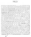
- FIG. 3shows 50 ⁇ m X 400 ⁇ m rectangles 300 within the tiles of a 16mm X 16mm chip area. These rectangles represent the area required for clock-trimming and calibrating circuitry associated with each tile. The circuitry in these rectangles is more than adequate for providing very robust clock trimming and calibration, and it is clear from the figure that the area involved is trivial.
- FIG. 4shows a preferred wiring layout of the clock tree on the secondary substrate configured in the form of a binary tree. Note that the distance to each leaf node 400 from the primary clock input 402 is exactly the same, and the load fanning out in each direction from each fanout node is exactly the same. Located at each leaf node is a driver circuit (not shown) for driving the output pin at the leaf node.
- the clock trimming circuit(or controlling means) contains scan-only control latches whose states cause the circuit to move clock edges back relative to the reference (input clock) signal prior to fanning the clock signal out.
- Each tile in FIG. 3has its own state control latches and all of these latches are connected in a single scan ring on the secondary substrate.
- Clock skewcan further be controlled in accordance with this invention via probing the transmitted clock signals on the primary (or secondary) substrates, and then adjusting clock edges via the scan ring. This is a standard technique.
- the circuit of FIG. 9operates as follows.
- a global clock signal to be shiftedarrives at trimming circuit of FIG. 9 at the input 901 of a course delay circuit 903.
- the course delay circuitcomprises delay elements that delay the input signal by 100 ps.
- a multiplexer 905selects either the delayed or undelayed signal as controlled by control latch 900a.
- the output of the multiplexer 905is provided to a fine delay circuit 904 which also comprises delay elements for delaying the signal in increments of 25 ps.
- a multiplexer 902selects the desired output signal as controlled by control latches 900b and 900c.
- the output of the multiplexer 902is a delayed version of the signal originally input to circuit 904 delayed by an integral multiple of 25 ps.
- This quiet-bus techniquecan not be done on the primary substrate because the metal levels on that substrate are heavily utilised, and the ambient noise is too great for the technique to work.
- the clock-distribution networkrequires only a trivial portion of the available wiring channels, most wiring channels on the secondary substrate (including perhaps several entire metal levels) can be grounded so as to provide a highly-shielded (quiet) environment for the few signals that are actually run across the secondary substrate.
- FIG. 5shows a signal wire on the quiet bus. Because the environment is very quiet, the wire can be precharged to an intermediate voltage level via a very-high-impedance precharging circuit 500. This precharging circuit leaks constantly, but the high impedance keeps the leakage low. This circuit could not be used in a noisy environment, because coupled noise could fairly easily pull the precharged circuit in either direction at random.
- the input to the wireis a clocked passgate 502 that takes a short sample of the static input, and allows that small sample to pull the precharged bus rapidly in the appropriate direction before allowing the bus to reach a quiescent point near its precharged state. This results in a travelling wave whose velocity is related to the characteristic impedance of the wire. The signal reaches the far end much faster than it would take for any driver circuit to charge the wire, which would be the standard transmission means in a noisy environment.
- the small-signal pulseis converted into a static signal by a standard driver 504 at the far end.
- processor chiphas a private DRAM that acts like a large L2 cache.
- microprocessor and the L2are distinct chips that are mounted on a MultiChip Module (MCM) in close proximity.
- MCMMultiChip Module
- the worst-case signal travel distanceis roughly three chip "pitches" (three sides of a chip), and can possibly be managed down to two chip pitches with efficient design.
- the standby poweris typically very low, and in accordance with this invention, the DRAM can be integral to the secondary substrate, and bonded directly onto the CP chip without causing a cooling problem.
- the worst-case distance in this scenariois determined by two chip pitches, and can possibly be managed down to below one chip pitch with efficient design.
- the "Finite Cache” contribution to the "Cycles Per Instruction” (CPI) performance measure for a processoris the product of the miss rate (misses per instruction) of the on-chip cache and the miss penalty (cycles per miss) associated with accessing the off-chip memory hierarchy.
- One component of this miss penaltyis the delay incurred by going from the CP chip to the L2, and back.
- FIGS. 6-8show various embodiments in accordance with the invention.
- the primary and secondary substratesare of comparable size, but are coupled via solderballs 600 in an offset manner so as to expose I/O pins 602 of the primary substrate and I/O pins 604 of the secondary substrate for external connection. As discussed above, both the primary and secondary substrates carry active circuitry.
- the primary substrateis somewhat smaller than the secondary substrate, so as to expose I/O pins of the secondary substrate for external connection. Again, both the primary and secondary substrates carry active circuitry.
- the inventioncan be extended to include a tertiary (and further) substrates as well, as shown in FIG. 8.
- the embodiment of FIG. 8includes a primary substrate 800, secondary substrate 802 and tertiary substrate 804.
- the primary and secondary substratesare bonded together by solder balls 806, positioned at corresponding I/O pads.
- External I/O pads 808 from the secondary substrateare bonded to pads on the tertiary substrate using the same C4 (flip-chip) technology.
- a trenchcan be provided in the tertiary substrate to accommodate the primary substrate.
- External I/O pins 810 of the tertiary substrateare exposed for external connection.
- Another benefit afforded by this inventionis that it results in a less expensive package.
- a multichip-module(second level package) is required using prior technology, and such second-level packaging requires an area that is proportional to two chips that the third-level package (e.g., card) must accommodate.
- processor/DRAM systemthat is made in accordance with this invention, there is no second-level package per se, since the DRAM secondary substrate is the "carrier" for the processor primary substrate. That processor/DRAM single-package entity can be wire-bonded or C4-bonded to the third-level package directly, and the area required is only proportional to the area of the secondary substrate (i.e., to the area of a single chip).
- the same third-level package that is used in such systems todaycould accommodate twice as many systems made in accordance with this invention.
Landscapes
- Engineering & Computer Science (AREA)
- Microelectronics & Electronic Packaging (AREA)
- Power Engineering (AREA)
- Computer Hardware Design (AREA)
- Physics & Mathematics (AREA)
- Condensed Matter Physics & Semiconductors (AREA)
- General Physics & Mathematics (AREA)
- Semiconductor Integrated Circuits (AREA)
- Dram (AREA)
- Wire Bonding (AREA)
Abstract
Description
Claims (10)
- A system comprising a primary chip (601) and a secondary chip (603) each havingactive components, said primary chip and secondary chip being connected to eachother face-to-face so that I/O pads (604) on at least the secondary chip remainaccessible to connection means outside of the system.
- The system in accordance with claim 1, wherein the primary and secondary chipsare coupled via solderballs (600).
- The system in accordance with claim 1 or 2, wherein the face of the primary chip(701) has a smaller area than the face of the secondary chip (702).
- The system in accordance with claim 1,2 or 3, wherein the primary and secondarychips (601,603) are connected face-to-face in an offset manner.
- The system in accordance with any of Claims 1 to 4 in which said primary chipcontains logic circuitry, and in which said secondary chip contains a clock distributionnetwork.
- The system in accordance with Claim 5, in which said clock distribution networkis a fanout tree with leaf nodes (400) placed on a regular grid, each said leaf nodecontaining an I/O driver circuit, each said I/O driver circuit driving an I/O padcentred at said gridpoint corresponding to said leafnode, each said I/O pad beingconnected to a corresponding I/O pad on the primary chip, each said I/O pad on saidprimary chip serving as a clock input, each said clock input being used to gate storageelements that are proximate and coupled to that input.
- The system in accordance with Claim 6 in which at least one of said I/O drivercircuits further contains a controlling means (903) for delaying the clock input byfixed amounts of time.
- The system in accordance with Claim 7, in which said controlling means storesstate information that specifies one of several fixed amounts of time, said stateinformation being retained by storage means settable by a scan operation.
- The system in accordance with claim 1, wherein at least one of said primary andsecondary chip contains inactive regions and regions of unused wiring tracks on oneor more metal wiring levels in which a plurality of wires in said wiring tracks areconnected to a common ground so that some wires in said wiring tracks are shieldedby said grounded wires.
- The system of any of claims 1 to 9, further comprising a tertiary chip having atrench for receiving the primary chip, and wherein the secondary chip is connected tothe tertiary chip face-to-face so that I/O pads on said tertiary chip remain accessible toconnection means outside of the system.
Applications Claiming Priority (2)
| Application Number | Priority Date | Filing Date | Title |
|---|---|---|---|
| US700261 | 1996-08-20 | ||
| US08/700,261US5760478A (en) | 1996-08-20 | 1996-08-20 | Clock skew minimization system and method for integrated circuits |
Publications (3)
| Publication Number | Publication Date |
|---|---|
| EP0827203A2true EP0827203A2 (en) | 1998-03-04 |
| EP0827203A3 EP0827203A3 (en) | 1998-04-15 |
| EP0827203B1 EP0827203B1 (en) | 2002-09-25 |
Family
ID=24812827
Family Applications (1)
| Application Number | Title | Priority Date | Filing Date |
|---|---|---|---|
| EP97305479AExpired - LifetimeEP0827203B1 (en) | 1996-08-20 | 1997-07-22 | Clock skew minimisation system and method for integrated circuits |
Country Status (9)
| Country | Link |
|---|---|
| US (2) | US5760478A (en) |
| EP (1) | EP0827203B1 (en) |
| JP (1) | JP3358171B2 (en) |
| KR (1) | KR100267430B1 (en) |
| CN (1) | CN1110097C (en) |
| DE (1) | DE69715762T2 (en) |
| MY (1) | MY117458A (en) |
| SG (1) | SG53009A1 (en) |
| TW (1) | TW357447B (en) |
Cited By (10)
| Publication number | Priority date | Publication date | Assignee | Title |
|---|---|---|---|---|
| WO1999066556A1 (en)* | 1998-06-16 | 1999-12-23 | Fraunhofer-Gesellschaft zur Förderung der angewandten Forschung e.V. | Vertically integrated microelectronic system and method for producing the same |
| WO2000041242A1 (en)* | 1998-12-30 | 2000-07-13 | Infineon Technologies Ag | Semiconductor unit |
| WO2000041241A1 (en)* | 1998-12-30 | 2000-07-13 | Infineon Technologies Ag | Vertically integrated semiconductor system |
| EP1069686A3 (en)* | 1999-07-15 | 2003-01-02 | Altera Corporation | Programmable logic device with unified cell structure including signal interface bumps |
| WO2003067604A3 (en)* | 2002-02-08 | 2003-12-11 | Conti Temic Microelectronic | Circuit system with a printed board comprising a programmable memory element |
| WO2004112136A1 (en)* | 2003-06-12 | 2004-12-23 | Koninklijke Philips Electronics N.V. | Electronic device |
| WO2007062944A1 (en)* | 2005-11-29 | 2007-06-07 | Infineon Technologies Ag | 3-dimensional multichip module |
| WO2009024761A3 (en)* | 2007-08-17 | 2009-04-30 | Timothy James Regan | Stack of integrated circuits |
| EP2100332A4 (en)* | 2006-06-16 | 2012-06-06 | Intel Corp | Chip stack with a higher power chip on the outside of the stack |
| EP1814321B1 (en)* | 2004-11-12 | 2013-01-30 | Panasonic Corporation | Digital television receiver circuit module |
Families Citing this family (145)
| Publication number | Priority date | Publication date | Assignee | Title |
|---|---|---|---|---|
| US5354695A (en) | 1992-04-08 | 1994-10-11 | Leedy Glenn J | Membrane dielectric isolation IC fabrication |
| US6714625B1 (en) | 1992-04-08 | 2004-03-30 | Elm Technology Corporation | Lithography device for semiconductor circuit pattern generation |
| US5763943A (en)* | 1996-01-29 | 1998-06-09 | International Business Machines Corporation | Electronic modules with integral sensor arrays |
| US5856914A (en)* | 1996-07-29 | 1999-01-05 | National Semiconductor Corporation | Micro-electronic assembly including a flip-chip mounted micro-device and method |
| US6687842B1 (en)* | 1997-04-02 | 2004-02-03 | Tessera, Inc. | Off-chip signal routing between multiply-connected on-chip electronic elements via external multiconductor transmission line on a dielectric element |
| JP2964983B2 (en)* | 1997-04-02 | 1999-10-18 | 日本電気株式会社 | Three-dimensional memory module and semiconductor device using the same |
| US6551857B2 (en) | 1997-04-04 | 2003-04-22 | Elm Technology Corporation | Three dimensional structure integrated circuits |
| US5915167A (en) | 1997-04-04 | 1999-06-22 | Elm Technology Corporation | Three dimensional structure memory |
| US6281590B1 (en)* | 1997-04-09 | 2001-08-28 | Agere Systems Guardian Corp. | Circuit and method for providing interconnections among individual integrated circuit chips in a multi-chip module |
| DE19743344C2 (en)* | 1997-09-30 | 1999-08-05 | Siemens Ag | Process for assembling integrated circuits with protection of the circuits against electrostatic discharge and corresponding arrangement of integrated circuits with protection against electrostatic discharge |
| US6037822A (en)* | 1997-09-30 | 2000-03-14 | Intel Corporation | Method and apparatus for distributing a clock on the silicon backside of an integrated circuit |
| CA2218307C (en)* | 1997-10-10 | 2006-01-03 | Gennum Corporation | Three dimensional packaging configuration for multi-chip module assembly |
| JP3441948B2 (en)* | 1997-12-12 | 2003-09-02 | 富士通株式会社 | Clock distribution circuit in semiconductor integrated circuit |
| US5869895A (en)* | 1997-12-15 | 1999-02-09 | Micron Technology, Inc. | Embedded memory assembly |
| US6198168B1 (en) | 1998-01-20 | 2001-03-06 | Micron Technologies, Inc. | Integrated circuits using high aspect ratio vias through a semiconductor wafer and method for forming same |
| US6090636A (en)* | 1998-02-26 | 2000-07-18 | Micron Technology, Inc. | Integrated circuits using optical waveguide interconnects formed through a semiconductor wafer and methods for forming same |
| US6150188A (en) | 1998-02-26 | 2000-11-21 | Micron Technology Inc. | Integrated circuits using optical fiber interconnects formed through a semiconductor wafer and methods for forming same |
| US6091138A (en)* | 1998-02-27 | 2000-07-18 | Advanced Micro Devices, Inc. | Multi-chip packaging using bump technology |
| US6150724A (en)* | 1998-03-02 | 2000-11-21 | Motorola, Inc. | Multi-chip semiconductor device and method for making the device by using multiple flip chip interfaces |
| US5977640A (en) | 1998-06-26 | 1999-11-02 | International Business Machines Corporation | Highly integrated chip-on-chip packaging |
| US6225699B1 (en) | 1998-06-26 | 2001-05-01 | International Business Machines Corporation | Chip-on-chip interconnections of varied characteristics |
| JP2000022074A (en)* | 1998-07-03 | 2000-01-21 | Rohm Co Ltd | Semiconductor device |
| US5854507A (en)* | 1998-07-21 | 1998-12-29 | Hewlett-Packard Company | Multiple chip assembly |
| US6674163B1 (en)* | 1998-08-18 | 2004-01-06 | Oki Electric Industry Co., Ltd. | Package structure for a semiconductor device |
| US6424034B1 (en) | 1998-08-31 | 2002-07-23 | Micron Technology, Inc. | High performance packaging for microprocessors and DRAM chips which minimizes timing skews |
| KR100470386B1 (en)* | 1998-12-26 | 2005-05-19 | 주식회사 하이닉스반도체 | Multi-chip Package |
| US6201302B1 (en)* | 1998-12-31 | 2001-03-13 | Sampo Semiconductor Corporation | Semiconductor package having multi-dies |
| JP2000223657A (en)* | 1999-02-03 | 2000-08-11 | Rohm Co Ltd | Semiconductor device and semiconductor chip used for the same |
| US6204562B1 (en)* | 1999-02-11 | 2001-03-20 | United Microelectronics Corp. | Wafer-level chip scale package |
| US6215193B1 (en)* | 1999-04-21 | 2001-04-10 | Advanced Semiconductor Engineering, Inc. | Multichip modules and manufacturing method therefor |
| US6386456B1 (en)* | 1999-06-04 | 2002-05-14 | International Business Machines Corporation | Memory card identification system |
| US6239484B1 (en) | 1999-06-09 | 2001-05-29 | International Business Machines Corporation | Underfill of chip-under-chip semiconductor modules |
| US6232667B1 (en)* | 1999-06-29 | 2001-05-15 | International Business Machines Corporation | Technique for underfilling stacked chips on a cavity MLC module |
| US6255899B1 (en) | 1999-09-01 | 2001-07-03 | International Business Machines Corporation | Method and apparatus for increasing interchip communications rates |
| US6500694B1 (en) | 2000-03-22 | 2002-12-31 | Ziptronix, Inc. | Three dimensional device integration method and integrated device |
| US6984571B1 (en) | 1999-10-01 | 2006-01-10 | Ziptronix, Inc. | Three dimensional device integration method and integrated device |
| US6376914B2 (en)* | 1999-12-09 | 2002-04-23 | Atmel Corporation | Dual-die integrated circuit package |
| KR100673378B1 (en)* | 1999-12-17 | 2007-01-23 | 삼성전자주식회사 | Chip scale multilayer chip package and its manufacturing method |
| KR100401019B1 (en)* | 1999-12-30 | 2003-10-08 | 앰코 테크놀로지 코리아 주식회사 | semiconductor package and its manufacturing method |
| US6369448B1 (en) | 2000-01-21 | 2002-04-09 | Lsi Logic Corporation | Vertically integrated flip chip semiconductor package |
| US6902987B1 (en) | 2000-02-16 | 2005-06-07 | Ziptronix, Inc. | Method for low temperature bonding and bonded structure |
| US6316981B1 (en)* | 2000-03-13 | 2001-11-13 | Intel Corporation | Signal distribution network on backside of substrate |
| US6437990B1 (en)* | 2000-03-20 | 2002-08-20 | Agere Systems Guardian Corp. | Multi-chip ball grid array IC packages |
| US6731009B1 (en)* | 2000-03-20 | 2004-05-04 | Cypress Semiconductor Corporation | Multi-die assembly |
| US6735755B2 (en)* | 2000-03-27 | 2004-05-11 | Jeng-Jye Shau | Cost saving methods using pre-defined integrated circuit modules |
| US7247932B1 (en)* | 2000-05-19 | 2007-07-24 | Megica Corporation | Chip package with capacitor |
| US6563133B1 (en)* | 2000-08-09 | 2003-05-13 | Ziptronix, Inc. | Method of epitaxial-like wafer bonding at low temperature and bonded structure |
| JP3829050B2 (en)* | 2000-08-29 | 2006-10-04 | 松下電器産業株式会社 | Integrated electronic components |
| KR20020058201A (en)* | 2000-12-29 | 2002-07-12 | 마이클 디. 오브라이언 | Semiconductor package and its manufacturing method |
| TWI313507B (en)* | 2002-10-25 | 2009-08-11 | Megica Corporatio | Method for assembling chips |
| US6748994B2 (en)* | 2001-04-11 | 2004-06-15 | Avery Dennison Corporation | Label applicator, method and label therefor |
| US6658373B2 (en)* | 2001-05-11 | 2003-12-02 | Field Diagnostic Services, Inc. | Apparatus and method for detecting faults and providing diagnostics in vapor compression cycle equipment |
| JP3670625B2 (en)* | 2001-06-13 | 2005-07-13 | 松下電器産業株式会社 | Semiconductor device and manufacturing method thereof |
| US6662126B2 (en)* | 2001-08-14 | 2003-12-09 | Sun Microsystems, Inc. | Measuring skew using on-chip sampling |
| US7332819B2 (en)* | 2002-01-09 | 2008-02-19 | Micron Technology, Inc. | Stacked die in die BGA package |
| US6541847B1 (en) | 2002-02-04 | 2003-04-01 | International Business Machines Corporation | Packaging for multi-processor shared-memory system |
| US6635970B2 (en) | 2002-02-06 | 2003-10-21 | International Business Machines Corporation | Power distribution design method for stacked flip-chip packages |
| TW523890B (en)* | 2002-02-07 | 2003-03-11 | Macronix Int Co Ltd | Stacked semiconductor packaging device |
| US6730540B2 (en)* | 2002-04-18 | 2004-05-04 | Tru-Si Technologies, Inc. | Clock distribution networks and conductive lines in semiconductor integrated circuits |
| US7122904B2 (en)* | 2002-04-25 | 2006-10-17 | Macronix International Co., Ltd. | Semiconductor packaging device and manufacture thereof |
| US20050104211A1 (en)* | 2002-05-07 | 2005-05-19 | Shinji Baba | Semiconductor device having semiconductor chips mounted on package substrate |
| JP4601892B2 (en)* | 2002-07-04 | 2010-12-22 | ラムバス・インコーポレーテッド | Semiconductor device and bump manufacturing method of semiconductor chip |
| US6973793B2 (en)* | 2002-07-08 | 2005-12-13 | Field Diagnostic Services, Inc. | Estimating evaporator airflow in vapor compression cycle cooling equipment |
| US6659512B1 (en)* | 2002-07-18 | 2003-12-09 | Hewlett-Packard Development Company, L.P. | Integrated circuit package employing flip-chip technology and method of assembly |
| JP2004063579A (en)* | 2002-07-25 | 2004-02-26 | Renesas Technology Corp | Stacked semiconductor device |
| AU2003255254A1 (en) | 2002-08-08 | 2004-02-25 | Glenn J. Leedy | Vertical system integration |
| US7495326B2 (en)* | 2002-10-22 | 2009-02-24 | Unitive International Limited | Stacked electronic structures including offset substrates |
| TWI230447B (en)* | 2003-04-25 | 2005-04-01 | Advanced Semiconductor Eng | Multi-chips package |
| DE10319271A1 (en)* | 2003-04-29 | 2004-11-25 | Infineon Technologies Ag | Memory circuitry and manufacturing method |
| US7109092B2 (en) | 2003-05-19 | 2006-09-19 | Ziptronix, Inc. | Method of room temperature covalent bonding |
| US6825567B1 (en)* | 2003-08-19 | 2004-11-30 | Advanced Semiconductor Engineering, Inc. | Face-to-face multi-chip flip-chip package |
| US7098075B1 (en)* | 2004-01-29 | 2006-08-29 | Xilinx, Inc. | Integrated circuit and method of producing a carrier wafer for an integrated circuit |
| US7303941B1 (en) | 2004-03-12 | 2007-12-04 | Cisco Technology, Inc. | Methods and apparatus for providing a power signal to an area array package |
| US9466595B2 (en)* | 2004-10-04 | 2016-10-11 | Intel Corporation | Fabrication of stacked die and structures formed thereby |
| US7364945B2 (en) | 2005-03-31 | 2008-04-29 | Stats Chippac Ltd. | Method of mounting an integrated circuit package in an encapsulant cavity |
| US7354800B2 (en) | 2005-04-29 | 2008-04-08 | Stats Chippac Ltd. | Method of fabricating a stacked integrated circuit package system |
| US8055833B2 (en) | 2006-10-05 | 2011-11-08 | Google Inc. | System and method for increasing capacity, performance, and flexibility of flash storage |
| US7386656B2 (en) | 2006-07-31 | 2008-06-10 | Metaram, Inc. | Interface circuit system and method for performing power management operations in conjunction with only a portion of a memory circuit |
| US20080028136A1 (en) | 2006-07-31 | 2008-01-31 | Schakel Keith R | Method and apparatus for refresh management of memory modules |
| US8060774B2 (en) | 2005-06-24 | 2011-11-15 | Google Inc. | Memory systems and memory modules |
| US8081474B1 (en) | 2007-12-18 | 2011-12-20 | Google Inc. | Embossed heat spreader |
| US9507739B2 (en) | 2005-06-24 | 2016-11-29 | Google Inc. | Configurable memory circuit system and method |
| US8438328B2 (en)* | 2008-02-21 | 2013-05-07 | Google Inc. | Emulation of abstracted DIMMs using abstracted DRAMs |
| US8244971B2 (en) | 2006-07-31 | 2012-08-14 | Google Inc. | Memory circuit system and method |
| US7609567B2 (en) | 2005-06-24 | 2009-10-27 | Metaram, Inc. | System and method for simulating an aspect of a memory circuit |
| US8335894B1 (en) | 2008-07-25 | 2012-12-18 | Google Inc. | Configurable memory system with interface circuit |
| US8041881B2 (en) | 2006-07-31 | 2011-10-18 | Google Inc. | Memory device with emulated characteristics |
| US9542352B2 (en) | 2006-02-09 | 2017-01-10 | Google Inc. | System and method for reducing command scheduling constraints of memory circuits |
| US8796830B1 (en) | 2006-09-01 | 2014-08-05 | Google Inc. | Stackable low-profile lead frame package |
| US20080082763A1 (en) | 2006-10-02 | 2008-04-03 | Metaram, Inc. | Apparatus and method for power management of memory circuits by a system or component thereof |
| US8077535B2 (en) | 2006-07-31 | 2011-12-13 | Google Inc. | Memory refresh apparatus and method |
| US8090897B2 (en)* | 2006-07-31 | 2012-01-03 | Google Inc. | System and method for simulating an aspect of a memory circuit |
| US8397013B1 (en) | 2006-10-05 | 2013-03-12 | Google Inc. | Hybrid memory module |
| US8386722B1 (en) | 2008-06-23 | 2013-02-26 | Google Inc. | Stacked DIMM memory interface |
| US8327104B2 (en) | 2006-07-31 | 2012-12-04 | Google Inc. | Adjusting the timing of signals associated with a memory system |
| US9171585B2 (en) | 2005-06-24 | 2015-10-27 | Google Inc. | Configurable memory circuit system and method |
| US8130560B1 (en) | 2006-11-13 | 2012-03-06 | Google Inc. | Multi-rank partial width memory modules |
| US8089795B2 (en) | 2006-02-09 | 2012-01-03 | Google Inc. | Memory module with memory stack and interface with enhanced capabilities |
| US8359187B2 (en) | 2005-06-24 | 2013-01-22 | Google Inc. | Simulating a different number of memory circuit devices |
| US10013371B2 (en) | 2005-06-24 | 2018-07-03 | Google Llc | Configurable memory circuit system and method |
| US8111566B1 (en) | 2007-11-16 | 2012-02-07 | Google, Inc. | Optimal channel design for memory devices for providing a high-speed memory interface |
| WO2007028109A2 (en) | 2005-09-02 | 2007-03-08 | Metaram, Inc. | Methods and apparatus of stacking drams |
| US7456088B2 (en)* | 2006-01-04 | 2008-11-25 | Stats Chippac Ltd. | Integrated circuit package system including stacked die |
| US7768125B2 (en)* | 2006-01-04 | 2010-08-03 | Stats Chippac Ltd. | Multi-chip package system |
| US9632929B2 (en) | 2006-02-09 | 2017-04-25 | Google Inc. | Translating an address associated with a command communicated between a system and memory circuits |
| US7750482B2 (en)* | 2006-02-09 | 2010-07-06 | Stats Chippac Ltd. | Integrated circuit package system including zero fillet resin |
| US8704349B2 (en)* | 2006-02-14 | 2014-04-22 | Stats Chippac Ltd. | Integrated circuit package system with exposed interconnects |
| US7385299B2 (en)* | 2006-02-25 | 2008-06-10 | Stats Chippac Ltd. | Stackable integrated circuit package system with multiple interconnect interface |
| EP1835618A1 (en)* | 2006-03-16 | 2007-09-19 | STMicroelectronics S.r.l. | Reduction of the time for executing an externally commanded transfer of data in an integrated device |
| KR100800472B1 (en) | 2006-06-23 | 2008-02-04 | 삼성전자주식회사 | A semiconductor memory device for a stack package and a read data skew adjusting method thereof |
| US7724589B2 (en) | 2006-07-31 | 2010-05-25 | Google Inc. | System and method for delaying a signal communicated from a system to at least one of a plurality of memory circuits |
| KR100843214B1 (en)* | 2006-12-05 | 2008-07-02 | 삼성전자주식회사 | Planar multi-semiconductor chip package in which memory chip and processor chip are connected through through electrode |
| US8049323B2 (en)* | 2007-02-16 | 2011-11-01 | Taiwan Semiconductor Manufacturing Co., Ltd. | Chip holder with wafer level redistribution layer |
| US8228704B2 (en)* | 2007-02-28 | 2012-07-24 | Samsung Electronics Co., Ltd. | Stacked semiconductor chip package with shared DLL signal and method for fabricating stacked semiconductor chip package with shared DLL signal |
| KR101196483B1 (en)* | 2007-07-16 | 2012-11-01 | 삼성전자주식회사 | Stacked semiconductor device and signal distribution method |
| US8080874B1 (en)* | 2007-09-14 | 2011-12-20 | Google Inc. | Providing additional space between an integrated circuit and a circuit board for positioning a component therebetween |
| US20090091017A1 (en)* | 2007-10-09 | 2009-04-09 | Fjelstad Joseph C | Partitioned Integrated Circuit Package with Central Clock Driver |
| US7863960B2 (en)* | 2009-04-30 | 2011-01-04 | International Business Machines Corporation | Three-dimensional chip-stack synchronization |
| US8227904B2 (en) | 2009-06-24 | 2012-07-24 | Intel Corporation | Multi-chip package and method of providing die-to-die interconnects in same |
| TWI449339B (en)* | 2010-12-13 | 2014-08-11 | Ind Tech Res Inst | Apparatus for clock skew compensation |
| KR101774938B1 (en) | 2011-08-31 | 2017-09-06 | 삼성전자 주식회사 | Semiconductor package having supporting plate and method of forming the same |
| US9318785B2 (en) | 2011-09-29 | 2016-04-19 | Broadcom Corporation | Apparatus for reconfiguring an integrated waveguide |
| US9075105B2 (en) | 2011-09-29 | 2015-07-07 | Broadcom Corporation | Passive probing of various locations in a wireless enabled integrated circuit (IC) |
| US9570420B2 (en) | 2011-09-29 | 2017-02-14 | Broadcom Corporation | Wireless communicating among vertically arranged integrated circuits (ICs) in a semiconductor package |
| US8508029B2 (en)* | 2011-09-29 | 2013-08-13 | Broadcom Corporation | Semiconductor package including an integrated waveguide |
| US8670638B2 (en) | 2011-09-29 | 2014-03-11 | Broadcom Corporation | Signal distribution and radiation in a wireless enabled integrated circuit (IC) using a leaky waveguide |
| US9030253B1 (en) | 2012-05-30 | 2015-05-12 | Altera Corporation | Integrated circuit package with distributed clock network |
| US8984463B2 (en) | 2012-11-28 | 2015-03-17 | Qualcomm Incorporated | Data transfer across power domains |
| US9064077B2 (en) | 2012-11-28 | 2015-06-23 | Qualcomm Incorporated | 3D floorplanning using 2D and 3D blocks |
| US9536840B2 (en) | 2013-02-12 | 2017-01-03 | Qualcomm Incorporated | Three-dimensional (3-D) integrated circuits (3DICS) with graphene shield, and related components and methods |
| US9041448B2 (en) | 2013-03-05 | 2015-05-26 | Qualcomm Incorporated | Flip-flops in a monolithic three-dimensional (3D) integrated circuit (IC) (3DIC) and related methods |
| US9177890B2 (en) | 2013-03-07 | 2015-11-03 | Qualcomm Incorporated | Monolithic three dimensional integration of semiconductor integrated circuits |
| US9171608B2 (en) | 2013-03-15 | 2015-10-27 | Qualcomm Incorporated | Three-dimensional (3D) memory cell separation among 3D integrated circuit (IC) tiers, and related 3D integrated circuits (3DICS), 3DIC processor cores, and methods |
| US9543965B1 (en) | 2013-10-04 | 2017-01-10 | Altera Corporation | Interposer with embedded clock network circuitry |
| KR20170001238A (en)* | 2015-06-26 | 2017-01-04 | 에스케이하이닉스 주식회사 | Semiconductor package including step type substrate |
| US9893058B2 (en)* | 2015-09-17 | 2018-02-13 | Semiconductor Components Industries, Llc | Method of manufacturing a semiconductor device having reduced on-state resistance and structure |
| CN105810237B (en)* | 2016-03-15 | 2018-08-21 | 西安紫光国芯半导体有限公司 | One kind is about DRAM clock tree Wiring structure |
| US10580757B2 (en) | 2016-10-07 | 2020-03-03 | Xcelsis Corporation | Face-to-face mounted IC dies with orthogonal top interconnect layers |
| KR102393946B1 (en) | 2016-10-07 | 2022-05-03 | 엑셀시스 코포레이션 | Direct-bonded native interconnect and active base die |
| CN108108501B (en)* | 2016-11-25 | 2021-07-02 | 成都锐成芯微科技股份有限公司 | Delay control method of integrated circuit chip |
| US10475766B2 (en)* | 2017-03-29 | 2019-11-12 | Intel Corporation | Microelectronics package providing increased memory component density |
| JP2018182213A (en)* | 2017-04-19 | 2018-11-15 | 富士通株式会社 | Semiconductor device and method of manufacturing semiconductor device |
| WO2019079631A1 (en)* | 2017-10-20 | 2019-04-25 | Xcelsis Corporation | Face-to-face mounted ic dies with orthogonal top interconnect layers |
| KR20230097121A (en) | 2020-10-29 | 2023-06-30 | 아데이아 세미컨덕터 본딩 테크놀로지스 인코포레이티드 | Direct bonding method and structure |
| CN116953862A (en)* | 2022-04-19 | 2023-10-27 | 武汉光迅科技股份有限公司 | A 3D packaged optical transceiver component and its use method |
Family Cites Families (23)
| Publication number | Priority date | Publication date | Assignee | Title |
|---|---|---|---|---|
| JPS59224154A (en)* | 1983-06-03 | 1984-12-17 | Mitsubishi Electric Corp | Gate array |
| JPS60175444A (en)* | 1984-02-22 | 1985-09-09 | Hitachi Ltd | semiconductor equipment |
| JPS6235528A (en)* | 1985-08-08 | 1987-02-16 | Fujitsu Ltd | High density mounting method |
| JPS62272560A (en)* | 1986-05-20 | 1987-11-26 | Nec Corp | Clock circuit connecting structure for multichip package |
| US4755704A (en)* | 1987-06-30 | 1988-07-05 | Unisys Corporation | Automatic clock de-skewing apparatus |
| JPH02126685A (en)* | 1988-11-07 | 1990-05-15 | Seiko Epson Corp | solid state image sensor |
| US5399898A (en)* | 1992-07-17 | 1995-03-21 | Lsi Logic Corporation | Multi-chip semiconductor arrangements using flip chip dies |
| JP2871041B2 (en)* | 1990-09-06 | 1999-03-17 | 三菱電機株式会社 | Semiconductor device |
| JP3238395B2 (en)* | 1990-09-28 | 2001-12-10 | 株式会社東芝 | Semiconductor integrated circuit |
| EP0486829B1 (en)* | 1990-10-22 | 1997-04-23 | Seiko Epson Corporation | Semiconductor device and semiconductor device packaging system |
| US5109168A (en)* | 1991-02-27 | 1992-04-28 | Sun Microsystems, Inc. | Method and apparatus for the design and optimization of a balanced tree for clock distribution in computer integrated circuits |
| US5434453A (en)* | 1991-04-26 | 1995-07-18 | Hitachi, Ltd. | Semiconductor integrated circuit device and computer system using the same |
| JPH04346463A (en)* | 1991-05-24 | 1992-12-02 | Mitsubishi Electric Corp | microwave band package |
| US5331235A (en)* | 1991-06-01 | 1994-07-19 | Goldstar Electron Co., Ltd. | Multi-chip semiconductor package |
| US5164817A (en)* | 1991-08-14 | 1992-11-17 | Vlsi Technology, Inc. | Distributed clock tree scheme in semiconductor packages |
| JPH05129516A (en)* | 1991-11-01 | 1993-05-25 | Hitachi Ltd | Semiconductor device |
| US5260233A (en)* | 1992-11-06 | 1993-11-09 | International Business Machines Corporation | Semiconductor device and wafer structure having a planar buried interconnect by wafer bonding |
| JPH06244282A (en)* | 1993-02-15 | 1994-09-02 | Nec Corp | Semiconductor integrated circuit device |
| JP3354937B2 (en)* | 1993-04-23 | 2002-12-09 | イルビン センサーズ コーポレーション | An electronic module including a stack of IC chips each interacting with an IC chip fixed to the surface of the stack. |
| US5323060A (en)* | 1993-06-02 | 1994-06-21 | Micron Semiconductor, Inc. | Multichip module having a stacked chip arrangement |
| US5362986A (en)* | 1993-08-19 | 1994-11-08 | International Business Machines Corporation | Vertical chip mount memory package with packaging substrate and memory chip pairs |
| US5567654A (en)* | 1994-09-28 | 1996-10-22 | International Business Machines Corporation | Method and workpiece for connecting a thin layer to a monolithic electronic module's surface and associated module packaging |
| US5565816A (en)* | 1995-08-18 | 1996-10-15 | International Business Machines Corporation | Clock distribution network |
- 1996
- 1996-08-20USUS08/700,261patent/US5760478A/ennot_activeExpired - Lifetime
- 1997
- 1997-02-25TWTW086102287Apatent/TW357447B/ennot_activeIP Right Cessation
- 1997-06-13KRKR1019970024459Apatent/KR100267430B1/ennot_activeExpired - Fee Related
- 1997-07-07SGSG1997002395Apatent/SG53009A1/enunknown
- 1997-07-16MYMYPI97003236Apatent/MY117458A/enunknown
- 1997-07-18CNCN97117154Apatent/CN1110097C/ennot_activeExpired - Fee Related
- 1997-07-22DEDE69715762Tpatent/DE69715762T2/ennot_activeExpired - Lifetime
- 1997-07-22EPEP97305479Apatent/EP0827203B1/ennot_activeExpired - Lifetime
- 1997-08-13JPJP21839097Apatent/JP3358171B2/ennot_activeExpired - Fee Related
- 1997-10-20USUS08/954,709patent/US6040203A/ennot_activeExpired - Fee Related
Cited By (17)
| Publication number | Priority date | Publication date | Assignee | Title |
|---|---|---|---|---|
| WO1999066556A1 (en)* | 1998-06-16 | 1999-12-23 | Fraunhofer-Gesellschaft zur Förderung der angewandten Forschung e.V. | Vertically integrated microelectronic system and method for producing the same |
| WO2000041242A1 (en)* | 1998-12-30 | 2000-07-13 | Infineon Technologies Ag | Semiconductor unit |
| WO2000041241A1 (en)* | 1998-12-30 | 2000-07-13 | Infineon Technologies Ag | Vertically integrated semiconductor system |
| US6388320B2 (en) | 1998-12-30 | 2002-05-14 | Infineon Technologies Ag | Vertically integrated semiconductor configuration |
| EP1069686A3 (en)* | 1999-07-15 | 2003-01-02 | Altera Corporation | Programmable logic device with unified cell structure including signal interface bumps |
| EP1667325A1 (en)* | 1999-07-15 | 2006-06-07 | Altera Corporation | Programmable logic device with unified cell structure including signal interface bumps |
| WO2003067604A3 (en)* | 2002-02-08 | 2003-12-11 | Conti Temic Microelectronic | Circuit system with a printed board comprising a programmable memory element |
| WO2004112136A1 (en)* | 2003-06-12 | 2004-12-23 | Koninklijke Philips Electronics N.V. | Electronic device |
| EP1814321B1 (en)* | 2004-11-12 | 2013-01-30 | Panasonic Corporation | Digital television receiver circuit module |
| US8730401B2 (en) | 2004-11-12 | 2014-05-20 | Panasonic Corporation | Circuit module for use in digital television receiver for receiving digital television broadcasting wave signal |
| WO2007062944A1 (en)* | 2005-11-29 | 2007-06-07 | Infineon Technologies Ag | 3-dimensional multichip module |
| US8247910B2 (en) | 2005-11-29 | 2012-08-21 | Infineon Technologies Ag | Three-dimensional multichip module |
| US7986033B2 (en) | 2005-11-29 | 2011-07-26 | Infineon Technologies Ag | Three-dimensional multichip module |
| US8598718B2 (en) | 2005-11-29 | 2013-12-03 | Infineon Technologies Ag | Three-dimensional multichip module |
| US8786104B2 (en) | 2005-11-29 | 2014-07-22 | Infineon Technologies Ag | Three-dimensional multichip module |
| EP2100332A4 (en)* | 2006-06-16 | 2012-06-06 | Intel Corp | Chip stack with a higher power chip on the outside of the stack |
| WO2009024761A3 (en)* | 2007-08-17 | 2009-04-30 | Timothy James Regan | Stack of integrated circuits |
Also Published As
| Publication number | Publication date |
|---|---|
| DE69715762T2 (en) | 2003-04-24 |
| US6040203A (en) | 2000-03-21 |
| HK1006242A1 (en) | 1999-02-19 |
| MY117458A (en) | 2004-06-30 |
| EP0827203B1 (en) | 2002-09-25 |
| KR19980018136A (en) | 1998-06-05 |
| CN1110097C (en) | 2003-05-28 |
| TW357447B (en) | 1999-05-01 |
| US5760478A (en) | 1998-06-02 |
| JP3358171B2 (en) | 2002-12-16 |
| EP0827203A3 (en) | 1998-04-15 |
| DE69715762D1 (en) | 2002-10-31 |
| SG53009A1 (en) | 1998-09-28 |
| KR100267430B1 (en) | 2000-10-16 |
| CN1175805A (en) | 1998-03-11 |
| JPH10107065A (en) | 1998-04-24 |
Similar Documents
| Publication | Publication Date | Title |
|---|---|---|
| EP0827203B1 (en) | Clock skew minimisation system and method for integrated circuits | |
| EP0446039B1 (en) | A multi-segmented bus and method of operation | |
| US7930661B1 (en) | Software model for a hybrid stacked field programmable gate array | |
| US5432708A (en) | Multichip module integrated circuit device having maximum input/output capability | |
| CN115098432A (en) | Embedded network-on-chip accessible to programmable logic structure of programmable logic device in multi-dimensional die system | |
| WO1994013121A1 (en) | Module comprising ic memory stack dedicated to and structurally combined with an ic microprocessor | |
| Maheshwari et al. | Design of FPGAs with area I/O for field programmable MCM | |
| WO2025006155A1 (en) | Building multi-die fpgas using chip-on-wafer technology | |
| Rosenbaum et al. | A 16384-bit high-density CCD memory | |
| US7276399B1 (en) | Method of designing a module-based flip chip substrate design | |
| JPH05283607A (en) | Semiconductor integrated circuit device and computer system using the same | |
| Darnauer et al. | Field programmable multi-chip module (FPMCM)-an integration of FPGA and MCM technology | |
| HK1006242B (en) | Clock skew minimization system and method for integrated circuits | |
| KR20020064525A (en) | Two sides memory module sharing clock signal and wiring method thereof | |
| US20240348253A1 (en) | Modular fabric architecture in fpga products | |
| Ferry et al. | Scaling theory in modern VLSI | |
| US20240321716A1 (en) | Electronic Devices Having Oval Power Delivery Pads | |
| US20250323111A1 (en) | Scalable Thermal Diode Implementation in Monolithic and Multi-Die FPGAs | |
| Hirt et al. | The Use of Area I/C or a Look at Future Architectures | |
| Sander | Semiconductor memory circuits and technology | |
| Brunfaut et al. | Optical area I/O enhanced FPGA with 256 optical channels per chip | |
| Shrivastava et al. | Relative figures of merit for chip-to-MCM substrate interconnection methods | |
| Hirt et al. | Area I/O's potential for future processor systems | |
| Spandorfer | Large scale integration—An appraisal | |
| Zhu et al. | Hierarchical Clock Routing Scheme for Multi-Chip Modules Based on Area Pad Interconnection |
Legal Events
| Date | Code | Title | Description |
|---|---|---|---|
| PUAI | Public reference made under article 153(3) epc to a published international application that has entered the european phase | Free format text:ORIGINAL CODE: 0009012 | |
| PUAL | Search report despatched | Free format text:ORIGINAL CODE: 0009013 | |
| AK | Designated contracting states | Kind code of ref document:A2 Designated state(s):DE FR GB | |
| AX | Request for extension of the european patent | Free format text:AL;LT;LV;RO;SI | |
| AK | Designated contracting states | Kind code of ref document:A3 Designated state(s):AT BE CH DE DK ES FI FR GB GR IE IT LI LU MC NL PT SE | |
| AX | Request for extension of the european patent | Free format text:AL;LT;LV;RO;SI | |
| 17P | Request for examination filed | Effective date:19980610 | |
| AKX | Designation fees paid | Free format text:DE FR GB | |
| RBV | Designated contracting states (corrected) | Designated state(s):DE FR GB | |
| 17Q | First examination report despatched | Effective date:19991015 | |
| GRAG | Despatch of communication of intention to grant | Free format text:ORIGINAL CODE: EPIDOS AGRA | |
| GRAG | Despatch of communication of intention to grant | Free format text:ORIGINAL CODE: EPIDOS AGRA | |
| GRAH | Despatch of communication of intention to grant a patent | Free format text:ORIGINAL CODE: EPIDOS IGRA | |
| GRAH | Despatch of communication of intention to grant a patent | Free format text:ORIGINAL CODE: EPIDOS IGRA | |
| GRAA | (expected) grant | Free format text:ORIGINAL CODE: 0009210 | |
| AK | Designated contracting states | Kind code of ref document:B1 Designated state(s):DE FR GB | |
| REG | Reference to a national code | Ref country code:GB Ref legal event code:FG4D | |
| REF | Corresponds to: | Ref document number:69715762 Country of ref document:DE Date of ref document:20021031 | |
| ET | Fr: translation filed | ||
| PGFP | Annual fee paid to national office [announced via postgrant information from national office to epo] | Ref country code:FR Payment date:20030721 Year of fee payment:7 | |
| PLBE | No opposition filed within time limit | Free format text:ORIGINAL CODE: 0009261 | |
| STAA | Information on the status of an ep patent application or granted ep patent | Free format text:STATUS: NO OPPOSITION FILED WITHIN TIME LIMIT | |
| 26N | No opposition filed | Effective date:20030626 | |
| PGFP | Annual fee paid to national office [announced via postgrant information from national office to epo] | Ref country code:GB Payment date:20040701 Year of fee payment:8 | |
| PG25 | Lapsed in a contracting state [announced via postgrant information from national office to epo] | Ref country code:FR Free format text:LAPSE BECAUSE OF NON-PAYMENT OF DUE FEES Effective date:20050331 | |
| REG | Reference to a national code | Ref country code:FR Ref legal event code:ST | |
| PG25 | Lapsed in a contracting state [announced via postgrant information from national office to epo] | Ref country code:GB Free format text:LAPSE BECAUSE OF NON-PAYMENT OF DUE FEES Effective date:20050722 | |
| GBPC | Gb: european patent ceased through non-payment of renewal fee | Effective date:20050722 | |
| REG | Reference to a national code | Ref country code:DE Ref legal event code:R081 Ref document number:69715762 Country of ref document:DE Owner name:GLOBALFOUNDRIES INC., KY Free format text:FORMER OWNER: INTERNATIONAL BUSINESS MACHINES CORPORATION, ARMONK, NY, US Ref country code:DE Ref legal event code:R082 Ref document number:69715762 Country of ref document:DE Representative=s name:RICHARDT PATENTANWAELTE PARTG MBB, DE Ref country code:DE Ref legal event code:R081 Ref document number:69715762 Country of ref document:DE Owner name:GLOBALFOUNDRIES INC., KY Free format text:FORMER OWNER: INTERNATIONAL BUSINESS MACHINES CORPORATION, ARMONK, N.Y., US | |
| REG | Reference to a national code | Ref country code:DE Ref legal event code:R082 Ref document number:69715762 Country of ref document:DE Representative=s name:RICHARDT PATENTANWAELTE PARTG MBB, DE Ref country code:DE Ref legal event code:R081 Ref document number:69715762 Country of ref document:DE Owner name:GLOBALFOUNDRIES INC., KY Free format text:FORMER OWNER: GLOBALFOUNDRIES US 2 LLC (N.D.GES.DES STAATES DELAWARE), HOPEWELL JUNCTION, N.Y., US | |
| REG | Reference to a national code | Ref country code:FR Ref legal event code:TP Owner name:GLOBALFOUNDRIES INC., GB Effective date:20160829 | |
| PGFP | Annual fee paid to national office [announced via postgrant information from national office to epo] | Ref country code:DE Payment date:20160720 Year of fee payment:20 | |
| REG | Reference to a national code | Ref country code:DE Ref legal event code:R071 Ref document number:69715762 Country of ref document:DE |