EP0826238B1 - Semiconductor body with a substrate glued to a support body - Google Patents
Semiconductor body with a substrate glued to a support bodyDownload PDFInfo
- Publication number
- EP0826238B1 EP0826238B1EP97902534AEP97902534AEP0826238B1EP 0826238 B1EP0826238 B1EP 0826238B1EP 97902534 AEP97902534 AEP 97902534AEP 97902534 AEP97902534 AEP 97902534AEP 0826238 B1EP0826238 B1EP 0826238B1
- Authority
- EP
- European Patent Office
- Prior art keywords
- layer
- substrate
- spacer elements
- support body
- layers
- Prior art date
- Legal status (The legal status is an assumption and is not a legal conclusion. Google has not performed a legal analysis and makes no representation as to the accuracy of the status listed.)
- Expired - Lifetime
Links
- 239000000758substrateSubstances0.000titleclaimsabstractdescription62
- 239000004065semiconductorSubstances0.000titleclaimsabstractdescription44
- 125000006850spacer groupChemical group0.000claimsabstractdescription58
- 239000003292glueSubstances0.000claimsabstractdescription21
- 239000004020conductorSubstances0.000claimsdescription23
- 239000000463materialSubstances0.000claimsdescription20
- 239000011810insulating materialSubstances0.000claimsdescription11
- 238000000034methodMethods0.000claimsdescription9
- 238000004519manufacturing processMethods0.000claimsdescription7
- XUIMIQQOPSSXEZ-UHFFFAOYSA-NSiliconChemical compound[Si]XUIMIQQOPSSXEZ-UHFFFAOYSA-N0.000description16
- 229910052710siliconInorganic materials0.000description16
- 239000010703siliconSubstances0.000description16
- VYPSYNLAJGMNEJ-UHFFFAOYSA-NSilicium dioxideChemical compoundO=[Si]=OVYPSYNLAJGMNEJ-UHFFFAOYSA-N0.000description14
- 229910052814silicon oxideInorganic materials0.000description14
- 238000004026adhesive bondingMethods0.000description8
- 229910052751metalInorganic materials0.000description7
- 239000002184metalSubstances0.000description7
- 230000015572biosynthetic processEffects0.000description5
- 229910052581Si3N4Inorganic materials0.000description2
- 229910052782aluminiumInorganic materials0.000description2
- XAGFODPZIPBFFR-UHFFFAOYSA-NaluminiumChemical compound[Al]XAGFODPZIPBFFR-UHFFFAOYSA-N0.000description2
- 239000011521glassSubstances0.000description2
- 229920002120photoresistant polymerPolymers0.000description2
- HQVNEWCFYHHQES-UHFFFAOYSA-Nsilicon nitrideChemical compoundN12[Si]34N5[Si]62N3[Si]51N64HQVNEWCFYHHQES-UHFFFAOYSA-N0.000description2
- 239000000919ceramicSubstances0.000description1
- 238000005530etchingMethods0.000description1
- 238000005498polishingMethods0.000description1
- 238000003825pressingMethods0.000description1
- 229920003002synthetic resinPolymers0.000description1
- 239000000057synthetic resinSubstances0.000description1
Images


Classifications
- H—ELECTRICITY
- H01—ELECTRIC ELEMENTS
- H01L—SEMICONDUCTOR DEVICES NOT COVERED BY CLASS H10
- H01L23/00—Details of semiconductor or other solid state devices
- H01L23/32—Holders for supporting the complete device in operation, i.e. detachable fixtures
- H—ELECTRICITY
- H01—ELECTRIC ELEMENTS
- H01L—SEMICONDUCTOR DEVICES NOT COVERED BY CLASS H10
- H01L24/00—Arrangements for connecting or disconnecting semiconductor or solid-state bodies; Methods or apparatus related thereto
- H01L24/80—Methods for connecting semiconductor or other solid state bodies using means for bonding being attached to, or being formed on, the surface to be connected
- H01L24/83—Methods for connecting semiconductor or other solid state bodies using means for bonding being attached to, or being formed on, the surface to be connected using a layer connector
- H—ELECTRICITY
- H01—ELECTRIC ELEMENTS
- H01L—SEMICONDUCTOR DEVICES NOT COVERED BY CLASS H10
- H01L23/00—Details of semiconductor or other solid state devices
- H01L23/02—Containers; Seals
- H01L23/04—Containers; Seals characterised by the shape of the container or parts, e.g. caps, walls
- H—ELECTRICITY
- H01—ELECTRIC ELEMENTS
- H01L—SEMICONDUCTOR DEVICES NOT COVERED BY CLASS H10
- H01L23/00—Details of semiconductor or other solid state devices
- H01L23/02—Containers; Seals
- H01L23/10—Containers; Seals characterised by the material or arrangement of seals between parts, e.g. between cap and base of the container or between leads and walls of the container
- H—ELECTRICITY
- H01—ELECTRIC ELEMENTS
- H01L—SEMICONDUCTOR DEVICES NOT COVERED BY CLASS H10
- H01L24/00—Arrangements for connecting or disconnecting semiconductor or solid-state bodies; Methods or apparatus related thereto
- H01L24/01—Means for bonding being attached to, or being formed on, the surface to be connected, e.g. chip-to-package, die-attach, "first-level" interconnects; Manufacturing methods related thereto
- H01L24/26—Layer connectors, e.g. plate connectors, solder or adhesive layers; Manufacturing methods related thereto
- H—ELECTRICITY
- H01—ELECTRIC ELEMENTS
- H01L—SEMICONDUCTOR DEVICES NOT COVERED BY CLASS H10
- H01L2224/00—Indexing scheme for arrangements for connecting or disconnecting semiconductor or solid-state bodies and methods related thereto as covered by H01L24/00
- H01L2224/80—Methods for connecting semiconductor or other solid state bodies using means for bonding being attached to, or being formed on, the surface to be connected
- H01L2224/83—Methods for connecting semiconductor or other solid state bodies using means for bonding being attached to, or being formed on, the surface to be connected using a layer connector
- H01L2224/8319—Arrangement of the layer connectors prior to mounting
- H—ELECTRICITY
- H01—ELECTRIC ELEMENTS
- H01L—SEMICONDUCTOR DEVICES NOT COVERED BY CLASS H10
- H01L2224/00—Indexing scheme for arrangements for connecting or disconnecting semiconductor or solid-state bodies and methods related thereto as covered by H01L24/00
- H01L2224/80—Methods for connecting semiconductor or other solid state bodies using means for bonding being attached to, or being formed on, the surface to be connected
- H01L2224/83—Methods for connecting semiconductor or other solid state bodies using means for bonding being attached to, or being formed on, the surface to be connected using a layer connector
- H01L2224/838—Bonding techniques
- H01L2224/8385—Bonding techniques using a polymer adhesive, e.g. an adhesive based on silicone, epoxy, polyimide, polyester
- H—ELECTRICITY
- H01—ELECTRIC ELEMENTS
- H01L—SEMICONDUCTOR DEVICES NOT COVERED BY CLASS H10
- H01L2924/00—Indexing scheme for arrangements or methods for connecting or disconnecting semiconductor or solid-state bodies as covered by H01L24/00
- H01L2924/01—Chemical elements
- H01L2924/01013—Aluminum [Al]
- H—ELECTRICITY
- H01—ELECTRIC ELEMENTS
- H01L—SEMICONDUCTOR DEVICES NOT COVERED BY CLASS H10
- H01L2924/00—Indexing scheme for arrangements or methods for connecting or disconnecting semiconductor or solid-state bodies as covered by H01L24/00
- H01L2924/01—Chemical elements
- H01L2924/01058—Cerium [Ce]
- H—ELECTRICITY
- H01—ELECTRIC ELEMENTS
- H01L—SEMICONDUCTOR DEVICES NOT COVERED BY CLASS H10
- H01L2924/00—Indexing scheme for arrangements or methods for connecting or disconnecting semiconductor or solid-state bodies as covered by H01L24/00
- H01L2924/06—Polymers
- H01L2924/078—Adhesive characteristics other than chemical
- H01L2924/07802—Adhesive characteristics other than chemical not being an ohmic electrical conductor
Definitions
- the inventionrelates to a semiconductor device with a substrate having a plane surface on which a layer structure is formed in a number of layers, which substrate is fastened with its side on which the layer structure was formed to a plane support body by means of a layer of glue comprising spacer elements.
- the layer structuremay be formed, for example, in a layer of semiconductor material, a layer of insulating material, a layer of conductive material, and a layer of passivating material.
- the layer of semiconductor materialis formed, for example, on the surface of an insulating substrate. First one or several semiconductor elements are formed in the layer of semiconductor material. The layer of semiconductor material may subsequently be removed from the surface next to the semiconductor elements. Then the layer of insulating material is deposited. After the latter has been provided with contact windows, the layer of conductive material is deposited and a pattern of conductors is formed. The semiconductor elements are contacted by means of these conductor tracks. Finally, the layer of passivating material is deposited for protecting the semiconductor elements and the conductor tracks against outside influences.
- the support bodygives strength to the entire assembly after gluing, so that the substrate may be very thin.
- the processmay start, for example, with a silicon wafer on which a layer of silicon oxide and a layer of silicon are formed.
- the layer structureis subsequently provided in and on the silicon layer.
- the silicon waferis glued with its side on which the layer structure was formed to a support body.
- the siliconis removed from the side remote from the support body until the silicon oxide layer is reached.
- the substratein this case is formed by the comparatively thin layer of silicon oxide.
- Glueis provided for fastening the substrate to the support body, whereupon the substrate and the support body are pressed against each other.
- the spacer elementsachieve that the glue is not pressed out entirely from between the substrate and the support body and that the substrate and the support body are fastened parallel to one another with a certain defined interspacing.
- Such a semiconductor deviceis known from EP-A-570 224, where the spacer elements are globules of silicon oxide or synthetic resin.
- a planarizing layeris also provided on the substrate.
- planarizing layer used in the known device described in fastening the substrate to the support bodyrenders the manufacture of the device complicated and thus expensive.
- His known from WO-A-92 17901 to glue a ceramic plate to a multichip module.
- the inventionhas for its object inter alia to provide a semiconductor device of the kind mentioned in the opening paragraph in which the fastening of the substrate to the support body can be achieved in a simpler manner.
- the semiconductor deviceis for this purpose characterized in that the spacer elements are fastened on the surface of the substrate and all have an equal height measured from the surface.
- the upper tips of the spacer elementsdefine a plane which extends parallel to the surface of the substrate.
- the substrate and the plane support bodyWhen the substrate and the plane support body are pressed together after the addition of glue, the substrate and the support body will be fastened to one another in parallel.
- the pressureis evenly distributed over all spacer elements during this. This is not the case when loose spacer elements in the form of globules are used, without the use of a planarizing layer.
- the layer structure formed on the substrate surface itselfis not plane. Without a planarizing layer, globules could lie on the non-plane surface of the layer structure, with the result that the pressure during gluing is absorbed by only a few globules. Very great forces could thus occur locally on the layer structure, which could cause damage.
- the use of the planarizing layer in the device known from EP-A-570 224serves to distribute the pressure evenly over the spacer elements during gluing.
- the spacer elementsmay be formed in a layer of a comparatively hard material such as, for example, silicon oxide, which is provided on the substrate separately from the other layers. This layer may be provided in any thickness desired, so that the interspacing between the surface of the substrate and the support body may be adjusted to any desired value.
- the formation of spacer elements in this mannerdoes require additional process steps. These additional process steps are avoided when the spacer elements are formed in a stack of those layers in which the layer structure is formed anyway. No extra layer need be deposited, and a pattern of spacer elements may be realized simultaneously with the formation of the layer structure and by means of the same photoresist masks.
- the layer structureIn determining which layers are to be included in said stack, it should be ascertained how high the layer structure will be on the surface of the substrate. This is not necessary if the stack comprises all layers in which the layer structure is formed. The spacer elements will then always be at least as high as the maximum thickness of the layer structure to be achieved.
- the pattern of spacer elementsis formed in a portion only of the layers of the stack.
- the patternmay be formed, for example, in all layers except in a passivating top layer.
- the spacer elementswill then be covered by this passivating layer.
- Other layers in the spacer elementsare protected in that case and do not come into contact, for example, with the glue by means of which the substrate and the support body are fastened to one another.
- the pattern of spacer elementsmay be formed, for example, only in this comparatively thick layer and not in the layers provided under and on the metal layer.
- the metal layeris comparatively thick, it is possible to etch a profile therein which is practically not disturbed by the layers provided thereon such as, for example, a much thinner layer of passivating material. It is thus achieved that substantially no glue layer is formed between the spacer elements and the support body during making of the glue connection. The distance between the surface of the substrate and the support body is then defined by the height of the spacer elements. A space saving on the substrate is possible here if the spacer elements at the same time form circuit elements. In the comparatively thick metal layer mentioned above, for example, a coil may advantageously be formed.
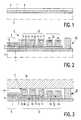
- Figs. 1 to 3diagrammatically and in cross-section show a few stages in the manufacture of a first semiconductor device with a substrate 1 on which a layer structure 2 is formed in a number of layers.
- the present examplestarts with a silicon wafer 3 on which an approximately 0.5 ⁇ m thick silicon oxide layer 1 is provided which will form the substrate of the semiconductor device, with an approximately 0.5 ⁇ m thick silicon layer 5.
- the silicon layer 5may be a monocrystalline layer as well as an amorphous or polycrystalline layer.
- One or several semiconductor elements 6such as diodes, transistors, or circuits comprising transistors are first formed in the silicon layer 5 in a usual manner. Only one semiconductor element 6 is depicted in the Figures very diagrammatically so as to keep the drawing simple.
- the silicon layer 5is removed from the surface 4 next to the semiconductor element 6 once the latter has been formed.
- a layer of insulating material 7 of, for example, silicon oxideis deposited.
- a layer of conductive material 9is deposited and a pattern of conductors is etched therein.
- a conductor 10 belonging to this patternis shown, connecting the semiconductor element 6 to an end 11 of a coil 12 yet to be formed.
- a further layer of insulating material 13, i.e. silicon oxide,is now provided and is given a contact window 14, whereupon a comparatively thick metal layer 15, for example aluminum, is deposited in which the coil 12 having turns 16 is formed.
- a layer of passivating material 17, for example silicon nitrideis deposited.
- the layer structure 2is formed on the surface 4 of the substrate 1, in this first example in the layers of semiconductor material 4, insulating material 7, conductive material 9, insulating material 13, conductive material 15, and passivating material 17.
- the layer of conductive material 15 in which the coil 12 is formedis approximately 3 ⁇ m thick, the other layers approximately 0.5 ⁇ m.
- the substrate 1is subsequently fastened with its side on which the layer structure 2 was formed to a plane, for example glass support body 18 by means of a glue layer 19 which encompasses spacer elements 20. After gluing, finally, the silicon is etched away from the wafer 3 on which the layer of silicon oxide forming the substrate 1 lies.
- the support bodygives strength to the entire assembly after gluing, so that the substrate 1 may be very thin.
- Glueis introduced during fastening of the substrate 1 to the support body 18, whereupon the substrate 1 and the support body 18 are pressed against each other.
- the spacer elements 20achieve that the glue is not pressed out entirely from between the substrate 1 and the support body 18, and the substrate 1 and support body 18 are fastened to one another in parallel with a certain defined interspacing.
- Figs. 4 to 6diagrammatically and in cross-section show a few stages in the manufacture of a second semiconductor device. Corresponding components and layers have been given the same reference numerals in these Figures as in the Figs. 1 to 3.
- the manufacture of the second semiconductor bodystarts with a silicon wafer 3 on which an approximately 0.5 ⁇ m thick silicon oxide layer 1 is provided which will form the substrate of the semiconductor device.
- First one or several semiconductor elements 6such as diodes, transistors, or circuits comprising transistors are formed in the silicon wafer 3 in a usual manner for the second semiconductor device. Only one semiconductor element 6 is depicted very diagrammatically in the Figures so as to keep the drawing simple.
- the layer structureis provided on the surface 4 of the substrate 1.
- the silicon oxide layer 1is provided with a contact window 21 for contacting the semiconductor element 6, whereupon a layer of conductive material 9 is deposited in which a pattern of conductors is etched. A conductor 10 of this pattern is shown in the drawing, connecting the semiconductor element 6 to an end 11 of a coil 12 yet to be formed.
- a layer of insulating material 13 of silicon oxidehas been provided and given a contact window 14, a comparatively thick metal layer 15, for example aluminum, is deposited, and the coil 12 having turns 16 is formed therein.
- a layer of a passivating material 17such as, for example, silicon nitride is deposited.
- the layer structure 2has thus been formed on the surface 4 of the substrate 1 in the layers of conductive material 9, insulating material 13, conductive material 15, and passivating material 17.
- the layer of conductive material 15 in which the coil 12 was formedis approximately 3 ⁇ m thick, the other layers approximately 0.5 ⁇ m.
- the substrate 1is fastened with its side on which the layer structure 2 was formed to a plane, for example glass support body 18 again in this second example by means of a glue layer 19 which encompasses spacer elements 20.
- the siliconis etched away from the wafer 3 on which the silicon oxide layer forming the substrate 1 lies, next to the semiconductor element 6 after gluing. This is done in this example in that first part of the silicon is removed in a polishing operation, subsequently an etching mask 22 is provided, and finally silicon is etched away in a KOH solution.
- the semiconductor element 6is now present in a small slice of semiconductor material 23 which lies at the side of the substrate facing away from the layer structure.
- the support bodygives strength to the entire assembly after gluing, so that the substrate 1 may be very thin.
- the coil 12lies on the thin insulating substrate 1 and accordingly has a high quality factor.
- spacer element 20Only one spacer element 20 is shown in each example, but it will be obvious that a pattern of such spacer elements will be provided, distributed over the entire wafer of semiconductor material 3. Since these elements all have the same height, it is achieved that the substrate 1 and the plane support body 18 are fastened to each other in parallel after the application of glue and after pressing together of the substrate and support body, the pressure being evenly distributed over all spacer elements 20.
- the spacer elements 20are formed in a layer of a comparatively hard material such as, for example, silicon oxide in the two devices shown in Figs. 3 and 6, which layer is provided separately from the other layers on the substrate 1.
- a layermay be provided to any desired thickness, so that the interspacing between the surface 4 of the substrate 1 and the support body 18 may be adjusted to any value as desired.
- the spacer elements 20are formed in a stack of the layers in which the layer structure 2 is formed, as shown in Figs. 7 to 10. It is not necessary then to deposit an extra layer.
- the pattern of spacer elements 20may then be realized simultaneously with the formation of the layer structure 2 and by means of the same photoresist masks.
- Figs. 7 to 10show a number of possible spacer elements which can be realized in the layers used in the first semiconductor device shown in Fig. 3. It will be obvious that similar spacer elements may be formed in the layers used in the second semiconductor device shown in Fig. 6.
- the turns 16 of the coil 12form the highest points in the layer structure 2. It is apparent from Fig. 3 that these highest points are formed by a stack of the layers of insulating material 7, conductive material 9, insulating material 13, conductive material 15, and passivating material 17.
- the spacer element 20is formed in a stack also comprising these layers 7, 9, 13, 15, 17.
- the spacer elements 20is as high as the highest point of the layer structure 2 in this case.
- Fig. 8shows the formation of a spacer element 20 formed in a stack of all layers which are provided on the surface 4 of the substrate 1.
- the spacer element shown in Fig. 8comprises besides the layers of the spacer element drawn in Fig. 7 also the layer of semiconductor material 5.
- the spacer elements 20are always at least as high as high as the maximum achievable thickness of the layer structure 2 in this case.
- the pattern of spacer elements 20is formed in only a portion of the layers of the stack.
- Fig. 9shows the formation of a spacer element 20 which is formed in a stack of layers 5, 7, 9, 13, 15 and 17, where only the layers 5, 7, 9, 13 and 15 are etched into a pattern.
- the spacer elements 20are entirely covered by the passivating layer 17.
- the other layers in the spacer elements 20are protected by this layer 17 and do not come into contact, for example, with the glue 19 by means of which the substrate I and the support body 18 are fastened to one another.
- FIG. 10shows spacer elements which double as turns 16 of the coil 12 formed in the comparatively thick layer of conductive material 15.
- the spacer elements 20are formed by those turns 16 of the coil 12 which lie on the layers 7, 9 and 13.
- the spacer elementsare accordingly formed in the layers 7, 9, 13, 15 and 17. Since the metal layer 15 is comparatively thick, it is possible to etch a profile therein which is substantially not disturbed by the layer 17 provided thereon. It is achieved thereby that substantially no glue layer 19 is formed between the spacer elements 20 and the support body 18 when the glue connection is being made.
Landscapes
- Engineering & Computer Science (AREA)
- Computer Hardware Design (AREA)
- Microelectronics & Electronic Packaging (AREA)
- Power Engineering (AREA)
- Physics & Mathematics (AREA)
- Condensed Matter Physics & Semiconductors (AREA)
- General Physics & Mathematics (AREA)
- Semiconductor Integrated Circuits (AREA)
- Pressure Sensors (AREA)
Abstract
Description
Claims (6)
- A method of manufacturing a semiconductor device, in which method on asubstrate (1) having a plane surface (4) a layer structure (2) is formed comprising a number oflayers including layers of insulating material (7,13), layers of conductive material (9,15) and alayer of passivating material (17), whereby in the layers of conductive material conductortracks (10) are formed which are connected with semiconductor elements (6) formed in a layerof semiconductor material (5,3), whereupon the substrate is fastened with its side on which thelayer structure was formed to a plane support body (18) by means of a layer of glue (19),whereby in the glue layer spacer elements (20) are provided having upper tips defining a planewhich extends parallel to the plane surface (4) of the substrate, on which tips the plane supportbody is pressed during fastening the substrate to the support bodysuch that substantially no glue is present between thespacer elements (20) and the support body (4),characterized in that, beforethe step of fastening the substrate to the plane support body, the spacer elements (20) areformed directly on the surface (4) of the substrate (1).
- A method as claimed in claim 1,characterized in that the spacer elements (20)are formed in a stack of those layers (7,9,13,15,17) in which the layer structure is formed.
- A method as claimed in claim 2,characterized in that the spacer elements (20)are formed in a stack comprising all layers in which the layer structure is formed.
- A method as claimed in claim 2 or 3,characterized in that a pattern for thespacer elements (20) is formed in only a portion of the layers of the stack.
- A method as claimed in claim 4,characterized in that the spacer elements areformed in the form of a circuit element.
- A method as claimed in claim 5,characterized in that the spacer elements areformed in the form of a coil (12).
Priority Applications (1)
| Application Number | Priority Date | Filing Date | Title |
|---|---|---|---|
| EP97902534AEP0826238B1 (en) | 1996-03-12 | 1997-02-25 | Semiconductor body with a substrate glued to a support body |
Applications Claiming Priority (4)
| Application Number | Priority Date | Filing Date | Title |
|---|---|---|---|
| EP96200673 | 1996-03-12 | ||
| EP96200673 | 1996-03-12 | ||
| PCT/IB1997/000157WO1997034321A2 (en) | 1996-03-12 | 1997-02-25 | Semiconductor body with a substrate glued to a support body |
| EP97902534AEP0826238B1 (en) | 1996-03-12 | 1997-02-25 | Semiconductor body with a substrate glued to a support body |
Publications (2)
| Publication Number | Publication Date |
|---|---|
| EP0826238A2 EP0826238A2 (en) | 1998-03-04 |
| EP0826238B1true EP0826238B1 (en) | 2001-10-04 |
Family
ID=8223773
Family Applications (1)
| Application Number | Title | Priority Date | Filing Date |
|---|---|---|---|
| EP97902534AExpired - LifetimeEP0826238B1 (en) | 1996-03-12 | 1997-02-25 | Semiconductor body with a substrate glued to a support body |
Country Status (6)
| Country | Link |
|---|---|
| US (1) | US5828122A (en) |
| EP (1) | EP0826238B1 (en) |
| JP (1) | JP4633868B2 (en) |
| KR (1) | KR100513412B1 (en) |
| DE (1) | DE69707077T2 (en) |
| WO (1) | WO1997034321A2 (en) |
Citations (1)
| Publication number | Priority date | Publication date | Assignee | Title |
|---|---|---|---|---|
| WO1992017901A1 (en)* | 1991-03-27 | 1992-10-15 | Integrated System Assemblies Corporation | Multichip integrated circuit module and method of fabrication |
Family Cites Families (23)
| Publication number | Priority date | Publication date | Assignee | Title |
|---|---|---|---|---|
| DE3038261A1 (en)* | 1980-10-10 | 1982-04-29 | Standard Elektrik Lorenz Ag, 7000 Stuttgart | BUILDING UNIT WITH PIEZOELECTRIC RESONATORS |
| US4506238A (en)* | 1981-12-14 | 1985-03-19 | Toko, Inc. | Hybrid circuit device |
| JPS5918910A (en)* | 1982-07-23 | 1984-01-31 | Canon Inc | optical filter |
| US4626478A (en)* | 1984-03-22 | 1986-12-02 | Unitrode Corporation | Electronic circuit device components having integral spacers providing uniform thickness bonding film |
| US4635356A (en)* | 1984-12-28 | 1987-01-13 | Kabushiki Kaisha Toshiba | Method of manufacturing a circuit module |
| JPS62217633A (en)* | 1986-03-19 | 1987-09-25 | Fujitsu Ltd | Planar plate bonding method |
| JPH01146322A (en)* | 1987-12-03 | 1989-06-08 | Nissan Motor Co Ltd | Manufacture of solid coupled body |
| JPH0329829U (en)* | 1989-07-28 | 1991-03-25 | ||
| JPH0394188A (en)* | 1989-09-06 | 1991-04-18 | Hitachi Medical Corp | Multi-element radiation detector |
| JP3103981B2 (en)* | 1990-09-07 | 2000-10-30 | セイコーインスツルメンツ株式会社 | Semiconductor single crystal substrate liquid crystal panel device |
| JP2517182B2 (en)* | 1991-06-03 | 1996-07-24 | 富士通株式会社 | Semiconductor substrate and manufacturing method thereof |
| JP2907238B2 (en)* | 1991-01-31 | 1999-06-21 | キヤノン株式会社 | Image reading device |
| JP2675199B2 (en)* | 1991-02-20 | 1997-11-12 | シャープ株式会社 | Display device |
| JP2998326B2 (en)* | 1991-08-09 | 2000-01-11 | 富士ゼロックス株式会社 | Image reading device |
| JPH0563899A (en)* | 1991-08-30 | 1993-03-12 | Canon Inc | Picture reader |
| JPH05183135A (en)* | 1991-10-14 | 1993-07-23 | Sony Corp | Ccd image pickup device |
| JPH05183157A (en)* | 1992-01-07 | 1993-07-23 | Fujitsu Ltd | Double-sided gate field effect transistor and fabrication thereof |
| JP2821830B2 (en)* | 1992-05-14 | 1998-11-05 | セイコーインスツルメンツ株式会社 | Semiconductor thin film device and its application device and method of manufacturing semiconductor thin film device |
| JPH06289424A (en)* | 1993-04-02 | 1994-10-18 | Sanyo Electric Co Ltd | Transmission type display device |
| JPH0714982A (en)* | 1993-06-21 | 1995-01-17 | Hitachi Ltd | Semiconductor integrated circuit device and manufacturing method thereof |
| JP3218861B2 (en)* | 1994-05-17 | 2001-10-15 | ソニー株式会社 | Manufacturing method of liquid crystal display device |
| WO1996016443A1 (en)* | 1994-11-22 | 1996-05-30 | Philips Electronics N.V. | Semiconductor device with a carrier body on which a substrate with a semiconductor element is fastened by means of a glue layer and on which a pattern of conductor tracks is fastened |
| US5564181A (en)* | 1995-04-18 | 1996-10-15 | Draper Laboratory, Inc. | Method of fabricating a laminated substrate assembly chips-first multichip module |
- 1997
- 1997-02-25JPJP53238897Apatent/JP4633868B2/ennot_activeExpired - Fee Related
- 1997-02-25WOPCT/IB1997/000157patent/WO1997034321A2/enactiveIP Right Grant
- 1997-02-25EPEP97902534Apatent/EP0826238B1/ennot_activeExpired - Lifetime
- 1997-02-25DEDE69707077Tpatent/DE69707077T2/ennot_activeExpired - Lifetime
- 1997-02-25KRKR1019970708042Apatent/KR100513412B1/ennot_activeExpired - Lifetime
- 1997-03-12USUS08/815,253patent/US5828122A/ennot_activeExpired - Lifetime
Patent Citations (1)
| Publication number | Priority date | Publication date | Assignee | Title |
|---|---|---|---|---|
| WO1992017901A1 (en)* | 1991-03-27 | 1992-10-15 | Integrated System Assemblies Corporation | Multichip integrated circuit module and method of fabrication |
Also Published As
| Publication number | Publication date |
|---|---|
| US5828122A (en) | 1998-10-27 |
| DE69707077T2 (en) | 2002-06-06 |
| DE69707077D1 (en) | 2001-11-08 |
| EP0826238A2 (en) | 1998-03-04 |
| WO1997034321A2 (en) | 1997-09-18 |
| WO1997034321A3 (en) | 1997-10-23 |
| JPH11505672A (en) | 1999-05-21 |
| KR100513412B1 (en) | 2005-12-06 |
| KR19990014701A (en) | 1999-02-25 |
| JP4633868B2 (en) | 2011-02-16 |
Similar Documents
| Publication | Publication Date | Title |
|---|---|---|
| EP0740853B1 (en) | Semiconductor device with a carrier body on which a substrate with a semiconductor element is fastened by means of a glue layer and on which a pattern of conductor tracks is fastened | |
| US5731222A (en) | Externally connected thin electronic circuit having recessed bonding pads | |
| US5166096A (en) | Process for fabricating self-aligned contact studs for semiconductor structures | |
| US7411261B2 (en) | MEMS device and fabrication method thereof | |
| JP4538107B2 (en) | Semiconductor device having a glass support to which an insulating layer having a semiconductor element and a metallized layer is attached by an adhesive | |
| JPH1022457A (en) | Capacitance device, semiconductor device, and manufacturing method thereof | |
| US5352927A (en) | Self-aligned contact studs for semiconductor structures | |
| JPH09507612A (en) | Manufacturing method of three-dimensional circuit device | |
| US5677230A (en) | Method of making wide bandgap semiconductor devices | |
| EP0746875B1 (en) | Method of manufacturing semiconductor devices with semiconductor elements formed in a layer of semiconductor material glued on a support wafer | |
| EP0826238B1 (en) | Semiconductor body with a substrate glued to a support body | |
| US3513022A (en) | Method of fabricating semiconductor devices | |
| US5635428A (en) | Global planarization using a polyimide block | |
| US5736452A (en) | Method of manufacturing a hybrid integrated circuit | |
| US20020132392A1 (en) | Semiconductor device and method for manufacturing the same | |
| US4017769A (en) | Integrated circuits and method of producing the same | |
| US7307021B1 (en) | Method for planarizing a thin film | |
| KR100253586B1 (en) | Method for manufacturing cell aperture mask of semiconductor device | |
| KR960007642B1 (en) | Manufacturing method of semiconductor device | |
| KR100190065B1 (en) | Trench isolation method | |
| KR100313530B1 (en) | Pad forming method for semiconductor device | |
| KR100275940B1 (en) | Method of fabricating an interlayer in semiconductor devices | |
| JP3402843B2 (en) | Semiconductor integrated circuit and manufacturing method thereof | |
| KR19980041605A (en) | Formation method of contact opening | |
| JPH06236863A (en) | Manufacture of semiconductor device |
Legal Events
| Date | Code | Title | Description |
|---|---|---|---|
| PUAI | Public reference made under article 153(3) epc to a published international application that has entered the european phase | Free format text:ORIGINAL CODE: 0009012 | |
| AK | Designated contracting states | Kind code of ref document:A2 Designated state(s):DE FR GB IT NL | |
| 17P | Request for examination filed | Effective date:19980318 | |
| 17Q | First examination report despatched | Effective date:19990610 | |
| GRAG | Despatch of communication of intention to grant | Free format text:ORIGINAL CODE: EPIDOS AGRA | |
| GRAG | Despatch of communication of intention to grant | Free format text:ORIGINAL CODE: EPIDOS AGRA | |
| GRAH | Despatch of communication of intention to grant a patent | Free format text:ORIGINAL CODE: EPIDOS IGRA | |
| GRAH | Despatch of communication of intention to grant a patent | Free format text:ORIGINAL CODE: EPIDOS IGRA | |
| GRAA | (expected) grant | Free format text:ORIGINAL CODE: 0009210 | |
| AK | Designated contracting states | Kind code of ref document:B1 Designated state(s):DE FR GB IT NL | |
| PG25 | Lapsed in a contracting state [announced via postgrant information from national office to epo] | Ref country code:NL Free format text:LAPSE BECAUSE OF FAILURE TO SUBMIT A TRANSLATION OF THE DESCRIPTION OR TO PAY THE FEE WITHIN THE PRESCRIBED TIME-LIMIT Effective date:20011004 | |
| REF | Corresponds to: | Ref document number:69707077 Country of ref document:DE Date of ref document:20011108 | |
| REG | Reference to a national code | Ref country code:GB Ref legal event code:IF02 | |
| ET | Fr: translation filed | ||
| NLV1 | Nl: lapsed or annulled due to failure to fulfill the requirements of art. 29p and 29m of the patents act | ||
| PLBE | No opposition filed within time limit | Free format text:ORIGINAL CODE: 0009261 | |
| STAA | Information on the status of an ep patent application or granted ep patent | Free format text:STATUS: NO OPPOSITION FILED WITHIN TIME LIMIT | |
| 26N | No opposition filed | ||
| REG | Reference to a national code | Ref country code:GB Ref legal event code:746 Effective date:20021014 | |
| REG | Reference to a national code | Ref country code:FR Ref legal event code:D6 | |
| REG | Reference to a national code | Ref country code:GB Ref legal event code:732E | |
| REG | Reference to a national code | Ref country code:FR Ref legal event code:TP | |
| PGFP | Annual fee paid to national office [announced via postgrant information from national office to epo] | Ref country code:IT Payment date:20080227 Year of fee payment:11 | |
| PG25 | Lapsed in a contracting state [announced via postgrant information from national office to epo] | Ref country code:IT Free format text:LAPSE BECAUSE OF NON-PAYMENT OF DUE FEES Effective date:20080225 | |
| REG | Reference to a national code | Ref country code:FR Ref legal event code:LT Effective date:20120109 | |
| REG | Reference to a national code | Ref country code:DE Ref legal event code:R082 Ref document number:69707077 Country of ref document:DE Representative=s name:BOSCH JEHLE PATENTANWALTSGESELLSCHAFT MBH, DE | |
| REG | Reference to a national code | Ref country code:GB Ref legal event code:S47 Free format text:CANCELLATION OF ENTRY; APPLICATION BY FILING PATENTS FORM 15 WITHIN 4 WEEKS FROM THE DATE OF PUBLICATION OF THIS JOURNAL NXP B.V. SEMICONDUCTOR BODY WITH A SUBSTRATE GLUED TO A SUPPORT BODY APPLICATION BY PROPRIETOR TO CANCEL LICENCE OF RIGHT UNDER SECTION 47(1) FILED ON 16 DECEMBER 2011 | |
| REG | Reference to a national code | Ref country code:DE Ref legal event code:R085 Ref document number:69707077 Country of ref document:DE Effective date:20111223 | |
| REG | Reference to a national code | Ref country code:GB Ref legal event code:732E Free format text:REGISTERED BETWEEN 20120315 AND 20120321 | |
| REG | Reference to a national code | Ref country code:DE Ref legal event code:R082 Ref document number:69707077 Country of ref document:DE Representative=s name:BOSCH JEHLE PATENTANWALTSGESELLSCHAFT MBH, DE Effective date:20120224 Ref country code:DE Ref legal event code:R081 Ref document number:69707077 Country of ref document:DE Owner name:INVENSAS CORP., SAN JOSE, US Free format text:FORMER OWNER: NXP B.V., EINDHOVEN, NL Effective date:20120224 | |
| REG | Reference to a national code | Ref country code:FR Ref legal event code:TP Owner name:INVENSAS CORPORATION, US Effective date:20120522 | |
| REG | Reference to a national code | Ref country code:GB Ref legal event code:S47 Free format text:ENTRY CANCELLED; NOTICE IS HEREBY GIVEN THAT THE ENTRY ON THE REGISTER 'LICENCES OF RIGHT' UPON THE UNDERMENTIONED PATENT WAS CANCELLED ON 9 MAY 2012 INVENSAS CORPORATION SEMICONDUCTOR BODY WITH A SUBSTRATE GLUED TO A SUPPORT BODY | |
| PGFP | Annual fee paid to national office [announced via postgrant information from national office to epo] | Ref country code:DE Payment date:20130228 Year of fee payment:17 | |
| REG | Reference to a national code | Ref country code:DE Ref legal event code:R119 Ref document number:69707077 Country of ref document:DE | |
| REG | Reference to a national code | Ref country code:DE Ref legal event code:R119 Ref document number:69707077 Country of ref document:DE Effective date:20140902 | |
| PG25 | Lapsed in a contracting state [announced via postgrant information from national office to epo] | Ref country code:DE Free format text:LAPSE BECAUSE OF NON-PAYMENT OF DUE FEES Effective date:20140902 | |
| REG | Reference to a national code | Ref country code:FR Ref legal event code:PLFP Year of fee payment:20 | |
| PGFP | Annual fee paid to national office [announced via postgrant information from national office to epo] | Ref country code:GB Payment date:20160226 Year of fee payment:20 Ref country code:FR Payment date:20160217 Year of fee payment:20 | |
| REG | Reference to a national code | Ref country code:GB Ref legal event code:PE20 Expiry date:20170224 | |
| PG25 | Lapsed in a contracting state [announced via postgrant information from national office to epo] | Ref country code:GB Free format text:LAPSE BECAUSE OF EXPIRATION OF PROTECTION Effective date:20170224 |