EP0804059B1 - Structure for mounting an electrical module on a board - Google Patents
Structure for mounting an electrical module on a boardDownload PDFInfo
- Publication number
- EP0804059B1 EP0804059B1EP97106749AEP97106749AEP0804059B1EP 0804059 B1EP0804059 B1EP 0804059B1EP 97106749 AEP97106749 AEP 97106749AEP 97106749 AEP97106749 AEP 97106749AEP 0804059 B1EP0804059 B1EP 0804059B1
- Authority
- EP
- European Patent Office
- Prior art keywords
- board
- daughter board
- lead frames
- daughter
- input
- Prior art date
- Legal status (The legal status is an assumption and is not a legal conclusion. Google has not performed a legal analysis and makes no representation as to the accuracy of the status listed.)
- Expired - Lifetime
Links
- 229920005989resinPolymers0.000claimsdescription5
- 239000011347resinSubstances0.000claimsdescription5
- 229920000106Liquid crystal polymerPolymers0.000claimsdescription2
- 239000004977Liquid-crystal polymers (LCPs)Substances0.000claimsdescription2
- 239000002241glass-ceramicSubstances0.000claimsdescription2
- 229920006015heat resistant resinPolymers0.000claimsdescription2
- 239000011810insulating materialSubstances0.000claims1
- 239000002184metalSubstances0.000description11
- 229910000679solderInorganic materials0.000description8
- 230000003044adaptive effectEffects0.000description4
- 238000000034methodMethods0.000description3
- 238000007747platingMethods0.000description3
- 229910000906BronzeInorganic materials0.000description2
- OAICVXFJPJFONN-UHFFFAOYSA-NPhosphorusChemical compound[P]OAICVXFJPJFONN-UHFFFAOYSA-N0.000description2
- 238000003491arrayMethods0.000description2
- 239000010974bronzeSubstances0.000description2
- KUNSUQLRTQLHQQ-UHFFFAOYSA-Ncopper tinChemical compound[Cu].[Sn]KUNSUQLRTQLHQQ-UHFFFAOYSA-N0.000description2
- 239000006071creamSubstances0.000description2
- 229910001369BrassInorganic materials0.000description1
- UCKMPCXJQFINFW-UHFFFAOYSA-NSulphideChemical compound[S-2]UCKMPCXJQFINFW-UHFFFAOYSA-N0.000description1
- 239000010951brassSubstances0.000description1
- 230000009977dual effectEffects0.000description1
- 239000003822epoxy resinSubstances0.000description1
- 239000011521glassSubstances0.000description1
- 238000004519manufacturing processMethods0.000description1
- 229920000647polyepoxidePolymers0.000description1
- 229920006389polyphenyl polymerPolymers0.000description1
- 238000005476solderingMethods0.000description1
Images


Classifications
- H—ELECTRICITY
- H05—ELECTRIC TECHNIQUES NOT OTHERWISE PROVIDED FOR
- H05K—PRINTED CIRCUITS; CASINGS OR CONSTRUCTIONAL DETAILS OF ELECTRIC APPARATUS; MANUFACTURE OF ASSEMBLAGES OF ELECTRICAL COMPONENTS
- H05K3/00—Apparatus or processes for manufacturing printed circuits
- H05K3/36—Assembling printed circuits with other printed circuits
- H05K3/366—Assembling printed circuits with other printed circuits substantially perpendicularly to each other
- H—ELECTRICITY
- H01—ELECTRIC ELEMENTS
- H01R—ELECTRICALLY-CONDUCTIVE CONNECTIONS; STRUCTURAL ASSOCIATIONS OF A PLURALITY OF MUTUALLY-INSULATED ELECTRICAL CONNECTING ELEMENTS; COUPLING DEVICES; CURRENT COLLECTORS
- H01R12/00—Structural associations of a plurality of mutually-insulated electrical connecting elements, specially adapted for printed circuits, e.g. printed circuit boards [PCB], flat or ribbon cables, or like generally planar structures, e.g. terminal strips, terminal blocks; Coupling devices specially adapted for printed circuits, flat or ribbon cables, or like generally planar structures; Terminals specially adapted for contact with, or insertion into, printed circuits, flat or ribbon cables, or like generally planar structures
- H01R12/50—Fixed connections
- H01R12/51—Fixed connections for rigid printed circuits or like structures
- H01R12/52—Fixed connections for rigid printed circuits or like structures connecting to other rigid printed circuits or like structures
- H—ELECTRICITY
- H05—ELECTRIC TECHNIQUES NOT OTHERWISE PROVIDED FOR
- H05K—PRINTED CIRCUITS; CASINGS OR CONSTRUCTIONAL DETAILS OF ELECTRIC APPARATUS; MANUFACTURE OF ASSEMBLAGES OF ELECTRICAL COMPONENTS
- H05K2201/00—Indexing scheme relating to printed circuits covered by H05K1/00
- H05K2201/10—Details of components or other objects attached to or integrated in a printed circuit board
- H05K2201/10227—Other objects, e.g. metallic pieces
- H05K2201/10424—Frame holders
- H—ELECTRICITY
- H05—ELECTRIC TECHNIQUES NOT OTHERWISE PROVIDED FOR
- H05K—PRINTED CIRCUITS; CASINGS OR CONSTRUCTIONAL DETAILS OF ELECTRIC APPARATUS; MANUFACTURE OF ASSEMBLAGES OF ELECTRICAL COMPONENTS
- H05K2201/00—Indexing scheme relating to printed circuits covered by H05K1/00
- H05K2201/10—Details of components or other objects attached to or integrated in a printed circuit board
- H05K2201/10613—Details of electrical connections of non-printed components, e.g. special leads
- H05K2201/10742—Details of leads
- H05K2201/10886—Other details
- H05K2201/10946—Leads attached onto leadless component after manufacturing the component
- H—ELECTRICITY
- H05—ELECTRIC TECHNIQUES NOT OTHERWISE PROVIDED FOR
- H05K—PRINTED CIRCUITS; CASINGS OR CONSTRUCTIONAL DETAILS OF ELECTRIC APPARATUS; MANUFACTURE OF ASSEMBLAGES OF ELECTRICAL COMPONENTS
- H05K3/00—Apparatus or processes for manufacturing printed circuits
- H05K3/30—Assembling printed circuits with electric components, e.g. with resistor
- H05K3/32—Assembling printed circuits with electric components, e.g. with resistor electrically connecting electric components or wires to printed circuits
- H05K3/34—Assembling printed circuits with electric components, e.g. with resistor electrically connecting electric components or wires to printed circuits by soldering
- H05K3/3447—Lead-in-hole components
Definitions
- the present inventionrelates to a structure for mounting a module to a mother board tridimensionally by use of lead frames.
- DE-A-38 01 610discloses a multiple connector for connecting printed circuit boards carrying electronic parts with wiring boards.
- An arc-shaped bridgeis provided for connecting boards. One end of the bridge is secured to one of the boards and the other end is inserted into an opening in the respective other board.
- the bridgehas a contact surface contacting the conductive surface of the wiring board. Additionally, one of the boards may have a guide pin to be inserted in the other board.
- FR-A-2 608 328discloses with respect to a prior art embodiment a lead frame that is comb-shaped for nipping a daughter board at the pads . More precisely, the daughter board is received in the fork-type end portions of the respective lead frames, wherein the two outer fingers are arranged on one side of the board and the center finger is arranged on the opposite side of the board.
- EP-A-0 287 274describes a device generally similar to the device of FR-A-2 608 328 mentioned above. More precisely, this document discloses that each of the leads is assigned to a respective terminal. This configuration makes it difficult to position the leads relative to a daughter-card and then connect the former to the latter.
- metal fittings 20 for connectioneach has a pair of flat body portions 21.
- Each body portion 21has a number of parallel fingers 30 at its edge for gripping jumpers 35.
- a potbelley-like slitis formed in each finger 30 and open at its outer end.
- Lead terminals 22extend out from each metal fitting while through holes 19 are formed in a mother printed circuit board or mother board 11.
- the lead terminals 22are inserted in the through holes 19 and soldered to the mother board 11.
- a subprinted circuit board or daughter board 15has its edge or card edge 16 inserted in aligned slits 23 formed in the metal fittings 20.
- the daughter board 15is mounted to the mother board 11 in a vertical position.
- each jumper 35has its opposite end portions pressed into the aligned fingers 30 of the nearby metal fittings 20. In this condition, the metal fittings 20 are interconnected by the jumper 35.
- the above arrangement of the jumpers 35makes it needless to form a power supply pattern or similar broad pattern having a great current capacity on the mother board 11 or the daughter board 15; that is, the jumpers 35 play the role of such a broad pattern.
- FIG. 2shows a module mounting structure and method disclosed in Japanese Patent Laid-Open Publication No. 1-304796 also mentioned earlier.
- an IC part 42is mounted on the surface of a daughter board 41 by solder 43, constituting a module 44.
- a lead pin or lead frame 49has a generally L-shaped section. The horizontal portion of the lead frame 49 is inserted in a through hole 41a formed in the daughter board 41 and affixed to the board 41 by solder 46. The vertical portion of the lead frame 49 is inserted in a through hole 47a formed in the mother board 47 and then affixed to the board 47 by solder 48.
- a first problemis that the structures cannot easily deal with the increasing number of pins of a daughter board.
- the metal fitting 20 taught in Laid-Open Publication No. 2-68982has the slit 23 for nipping the edge of the daughter board 15, and the lead terminals 22 to be inserted in the through holes 19 of the mother board 11. Therefore, to accommodate a great number of pins, one metal fitting 20 must be assigned to each input/output terminal, resulting in complicated production.
- the lead frame taught in Laid-Open Publication No. 1-304796has its one end press fitted in the through hole 41a of the daughter board 41. In this configuration, the lead frame 49 can be press fitted from only one side of the daughter board 41. Therefore, to accommodate a great number of pins, the diameter and pitch of the through holes 41a must be reduced, or the size of the daughter board 41 must be increased, resulting in low yield.
- a second problemis that the conventional structures are not adaptive to dense module mounting. Specifically, the metal fitting 20 prevents the daughter boards 15 to be mounted to the mother board 11 at a small pitch because the the size of the metal fitting 20 limits the mounting pitch.
- a third problemis that the conventional structures are not adaptive to high speed operation.
- the metal fitting 20 taught in Laid-Open Publication No. 2-68982has a great surface area, and therefore a great capacitive load.
- a mother board 1carries a number of electronic parts, not shown, thereon.
- a plurality of patterns, not shown, to be connected to a daughter board 3are led out via the mother board 1, and each terminates at a respective through hole 2.
- Solder creamis printed on pads provided on the front and rear of the daughter board 3, and then a preselected electronic part 4 is mounted to the pads via the solder cream.
- a plurality of signal patterns, ground patterns and power supply patternsare led out at the end of the daughter board 3 adjoining the mother board 1 on each of the front and rear of the board 3.
- Input/output pads 7each is provided on the end of the respective pattern.
- a plurality of lead frames 5are affixed to an affixing member 6 and then respectively soldered to the input/output pads 7 at one end 5a thereof.
- the affixing member 6is formed of resin.
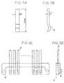
- FIGS. 5A-5Dshow a specific configuration of the lead frames 5 and a specific configuration of the affixing block formed of resin 6.
- the lead frames 5each having the configuration shown in FIGS. 5A and 5B are affixed to the affixing block 6, as shown in FIGS. 5C and 5D.
- the number of the lead frames 5is the same as the number of the input/output pads 7 provided on one side of the daughter board 3. Lugs 9 protrude from both ends of the lower portion of the affixing block 6, as illustrated.
- the electronic parts 4are mounted on the daughter board 3, as shown in FIG. 4 in detail.
- Reference holes 8(see FIG. 6) are formed in the daughter board 3 at both ends of the lower portion of the board 3.
- the lugs 9 of the affixing block 6are respectively received in the reference holes 8 in order to prevent the block 6 from being displaced relative to the daughter board 3.
- the lead frames 5are affixed to the respective affixing block 6 on each side of the daughter board 3, and soldered to the input/output pads 7. Such two arrays of lead frames 5 are respectively inserted in two arrays of through holes 2 formed in the mother board 1. Subsequently, the lead frames 5 are soldered to the mother board 1, as shown in FIG. 4.
- the lead frames 5are 5.955 mm long, 0.2 mm wide, and 0.1 mm thick each.
- the lead frames 5are formed of phosphor bronze, and each is provided with a 1 ⁇ m thick Ni plating and a 2 ⁇ m thick solder plating overlying the Ni plating. Phosphor bronze may be replaced with brass, if desired.
- the daughter board 3is implemented as a printed circuit board using glass epoxy resin or similar organic insulating resin although it may be implemented as a glass ceramic board.
- the resin constituting the affixing block 6use is made of a liquid crystal polymer although it may be replaced with polyphenyl sulfide or similar heat-resistant resin.
- the present inventionprovides a module mounting structure having various unprecedented advantages, as follows. Input/output terminals for different kinds of signals can be provided on both sides of a daughter board, implementing dense module mounting.
- the structureis therefore adaptive to an increase in the number of pins without increasing the size of a daughter board. Because daughter boards are inserted in through holes formed in a mother board and then soldered to the mother board, there can be reduced the pitch of the daughter boards.
- daughter boards and a mother boardare interconnected by the shortest distance, so that the structure of the present invention can deal with high speed operation.
- the interconnection distanceis short enough to make an inductance component and a capacitance component negligibly small.
- moduleslike other parts, can be collectively mounted to a mother board by solder reflow, and because the daughter board can be inserted in through holes and affixed by soldering together with other DIP (Dual In-Line Package) parts.
- DIPDual In-Line Package
Landscapes
- Engineering & Computer Science (AREA)
- Manufacturing & Machinery (AREA)
- Microelectronics & Electronic Packaging (AREA)
- Combinations Of Printed Boards (AREA)
- Multi-Conductor Connections (AREA)
- Coupling Device And Connection With Printed Circuit (AREA)
Description
- The present invention relates to a structure formounting a module to a mother board tridimensionally by useof lead frames.
- To meet the increasing demand for a miniature, denseand high-speed electronic apparatus, it is a common practiceto mount electronic parts and ICs (Integrated Circuits) to aprinted circuit board to constitute a module, and to mount anumber of such modules to a single mother boardtridimensionally. The prerequisite with this kind of scheme isthat the modules and mother board be electricallyinterconnected, mechanically surely supported, and low cost.Japanese Patent Laid-Open Publication No. 1-304796, forexample, discloses a module mounting method of this kind.Japanese Patent Laid-Open Publication No. 2-68982 teaches astructure for mounting a printed circuit board. However, theconventional structures cannot deal with an increase in thenumber of pins of the daughter board or an increase in thedensity or operation speed of the module.
- DE-A-38 01 610 discloses a multiple connector for connectingprinted circuit boards carrying electronic parts with wiringboards. An arc-shaped bridge is provided for connectingboards. One end of the bridge is secured to one of theboards and the other end is inserted into an opening in therespective other board. The bridge has a contact surfacecontacting the conductive surface of the wiring board.Additionally, one of the boards may have a guide pin to beinserted in the other board.
- FR-A-2 608 328 discloses with respect to a prior artembodiment a lead frame that is comb-shaped for nipping adaughter board at the pads . More precisely, the daughterboard is received in the fork-type end portions of therespective lead frames, wherein the two outer fingers arearranged on one side of the board and the center finger isarranged on the opposite side of the board.
- EP-A-0 287 274 describes a device generally similar to thedevice of FR-A-2 608 328 mentioned above. More precisely, thisdocument discloses that each of the leads is assigned to arespective terminal. This configuration makes it difficult toposition the leads relative to a daughter-card and thenconnect the former to the latter.
- It is therefore an object of the present invention toprovide a module mounting structure adaptive to an increasein the number of pins of a daughter board and an increase inoperation speed. This object is achieved with the features of the claims.
- The above and other objects, features and advantages ofthe present invention will become apparent from thefollowing detailed description taken with the accompanyingdrawings in which:
- FIG. 1A is a perspective view showing a conventionalmounting structure;
- FIG. 1B is a fragmentary enlarged perspective view ofthe structure shown in FIG. 1A;
- FIG. 2 is a section showing another conventionalmounting structure;
- FIG. 3 is a perspective view showing a mountingstructure embodying the present invention;
- FIG. 4 is a section along line A-A of FIG. 3;
- FIG. 5A shows a specific configuration of a lead frameand a specific configuration of an affixing member both ofwhich are included in the embodiment;
- FIG. 5B is a side elevation of the lead frame shown inFIG. 5A;
- FIG. 5C is a front view showing a plurality of lead framesaffixed to the affixing member;
- FIG. 5D is a side elevation showing the lead frames andaffixing block;
- FIG. 6 is a front view of a daughter board included in theembodiment; and
- FIG. 7 is a perspective view showing how the daughterboard is mounted to a mother board in the illustrativeembodiment.
- To better understand the present invention, briefreference will be made to a conventional structure formounting printed circuit boards, shown in FIGS. 1A and 1B.The structure to be described is taught in Japanese Patent Laid-Open Publication No. 2-68982 mentioned earlier. Asshown,
metal fittings 20 for connection each has a pair offlatbody portions 21. Eachbody portion 21 has a number ofparallel fingers 30 at its edge forgripping jumpers 35. Apotbelley-like slit is formed in eachfinger 30 and open at itsouter end. When thejumper 35 is inserted in the slit of anyone of thefingers 30, thefinger 30 grips the periphery of thejumper 35, as illustrated.Notches 31 are formed in theportions of thefingers 30 adjoining thebody portion 21, sothat needless ones of thefingers 30 can be easily bent andremoved by hand. Lead terminals 22 extend out from each metal fittingwhile throughholes 19 are formed in a mother printed circuitboard or mother board 11. Thelead terminals 22 are insertedin the throughholes 19 and soldered to the mother board 11.After themetal fittings 20 have been mounted to the motherboard 11 in a vertical array, a subprinted circuit board ordaughter board 15 has its edge orcard edge 16 inserted inalignedslits 23 formed in themetal fittings 20. As a result,thedaughter board 15 is mounted to the mother board 11 in avertical position. Subsequently, eachjumper 35 has itsopposite end portions pressed into the alignedfingers 30 ofthenearby metal fittings 20. In this condition, themetalfittings 20 are interconnected by thejumper 35.- The above arrangement of the
jumpers 35 makes itneedless to form a power supply pattern or similar broadpattern having a great current capacity on the mother board11 or thedaughter board 15; that is, thejumpers 35 play therole of such a broad pattern. - FIG. 2 shows a module mounting structure and methoddisclosed in Japanese Patent Laid-Open Publication No. 1-304796also mentioned earlier. As shown, an
IC part 42 ismounted on the surface of adaughter board 41 bysolder 43,constituting amodule 44. A lead pin orlead frame 49 has agenerally L-shaped section. The horizontal portion of theleadframe 49 is inserted in a through hole 41a formed in thedaughter board 41 and affixed to theboard 41 bysolder 46.The vertical portion of thelead frame 49 is inserted in athrough hole 47a formed in themother board 47 and thenaffixed to theboard 47 bysolder 48. - The conventional structures described above each hassome problems left unsolved, as follows. A first problem isthat the structures cannot easily deal with the increasingnumber of pins of a daughter board. Specifically, the
metalfitting 20 taught in Laid-Open Publication No. 2-68982 has theslit 23 for nipping the edge of thedaughter board 15, and thelead terminals 22 to be inserted in the throughholes 19 of themother board 11. Therefore, to accommodate a great numberof pins, onemetal fitting 20 must be assigned to each input/output terminal, resulting in complicated production.The lead frame taught in Laid-Open Publication No. 1-304796has its one end press fitted in the through hole 41a of thedaughter board 41. In this configuration, thelead frame 49can be press fitted from only one side of thedaughter board 41. Therefore, to accommodate a great number of pins, thediameter and pitch of the through holes 41a must be reduced,or the size of thedaughter board 41 must be increased,resulting in low yield. - A second problem is that the conventional structures arenot adaptive to dense module mounting. Specifically, the
metal fitting 20 prevents thedaughter boards 15 to bemounted to the mother board 11 at a small pitch because thethe size of the metal fitting 20 limits the mounting pitch. - A third problem is that the conventional structures arenot adaptive to high speed operation. For example, the metalfitting 20 taught in Laid-Open Publication No. 2-68982 has agreat surface area, and therefore a great capacitive load.
- Reference will be made to FIGS. 3 and 4 for describing apreferred embodiment of the module mounting structure inaccordance with the present invention. As shown, a motherboard 1 carries a number of electronic parts, not shown,thereon. A plurality of patterns, not shown, to be connected toa
daughter board 3 are led out via the mother board 1, andeach terminates at a respective throughhole 2. Solder cream is printed on pads provided on the front and rear of thedaughter board 3, and then a preselected electronic part 4 ismounted to the pads via the solder cream. A plurality ofsignal patterns, ground patterns and power supply patternsare led out at the end of thedaughter board 3 adjoining themother board 1 on each of the front and rear of theboard 3.Input/output pads 7 each is provided on the end of therespective pattern. On each of the front and rear of thedaughter board 3, a plurality oflead frames 5 are affixed toan affixingmember 6 and then respectively soldered to theinput/output pads 7 at oneend 5a thereof. The affixingmember 6 is formed of resin. - FIGS. 5A-5D show a specific configuration of the leadframes 5 and a specific configuration of the affixing blockformed of
resin 6. The lead frames 5 each having theconfiguration shown in FIGS. 5A and 5B are affixed to theaffixingblock 6, as shown in FIGS. 5C and 5D. The number ofthe lead frames 5 is the same as the number of theinput/output pads 7 provided on one side of thedaughterboard 3.Lugs 9 protrude from both ends of the lower portionof the affixingblock 6, as illustrated. The electronic parts 4are mounted on thedaughter board 3, as shown in FIG. 4 indetail. Reference holes 8 (see FIG. 6) are formed in thedaughter board 3 at both ends of the lower portion of theboard 3. Thelugs 9 of the affixingblock 6 are respectively received in the reference holes 8 in order to prevent theblock 6 from being displaced relative to thedaughter board 3. - As shown in FIG. 7, the lead frames 5 are affixed to the
respective affixing block 6 on each side of thedaughter board 3, and soldered to the input/output pads 7. Such two arraysoflead frames 5 are respectively inserted in two arrays ofthroughholes 2 formed in the mother board 1. Subsequently,the lead frames 5 are soldered to the mother board 1, asshown in FIG. 4. - As shown in FIGS. 5A and 5B, the lead frames 5 are5.955 mm long, 0.2 mm wide, and 0.1 mm thick each. Thelead frames 5 are formed of phosphor bronze, and each isprovided with a 1 µm thick Ni plating and a 2 µm thick solderplating overlying the Ni plating. Phosphor bronze may bereplaced with brass, if desired. In the illustrativeembodiment, the
daughter board 3 is implemented as aprinted circuit board using glass epoxy resin or similar organicinsulating resin although it may be implemented as a glassceramic board. In the embodiment, for the resin constitutingthe affixingblock 6, use is made of a liquid crystal polymeralthough it may be replaced with polyphenyl sulfide or similarheat-resistant resin. - In summary, it will be seen that the present inventionprovides a module mounting structure having variousunprecedented advantages, as follows. Input/output terminals for different kinds of signals can be provided onboth sides of a daughter board, implementing dense modulemounting. The structure is therefore adaptive to an increasein the number of pins without increasing the size of adaughter board. Because daughter boards are inserted inthrough holes formed in a mother board and then soldered tothe mother board, there can be reduced the pitch of thedaughter boards.
- Further, daughter boards and a mother board areinterconnected by the shortest distance, so that the structureof the present invention can deal with high speed operation.Specifically, the interconnection distance is short enough tomake an inductance component and a capacitance componentnegligibly small.
- Moreover, the structure is practicable with aconventional solder process and is therefore low cost. This isbecause modules, like other parts, can be collectively mountedto a mother board by solder reflow, and because the daughterboard can be inserted in through holes and affixed bysoldering together with other DIP (Dual In-Line Package)parts.
Claims (6)
- A module mounting structure comprising:a) a daughter board (3) carrying electronic parts (4) on both sides thereof, saiddaughter board (3) being provided with a plurality of input/output pads (7) on atleast one side thereof;b) an affixing member (6) for affixing a plurality of substantially straight lead frames(5), each of said lead frames (5) having one end thereof soldered to acorresponding one of said plurality of input/output pads (7); andc) a mother board (1) formed with a plurality of through holes (2) respectivelycorresponding to said plurality of input/output pads (7), wherein the other end ofeach of said lead frames (5) is inserted in and soldered to a corresponding one ofsaid plurality of through holes (2).
- The structure of claim 1, wherein a plurality of lead frames (5) is also soldered tosaid plurality of input/output pads (7) on the other side of said daughter board (3).
- The structure of claim 1 or 2, wherein said daughter board (3) comprises a printedcircuit board using an organic resin as an insulating material.
- The structure of any of claims 1 to 3, wherein said daughter board (3) comprises a glassceramic board.
- The structure of any of claims 1 to 4, wherein said affixing member (6) is formed of aliquid crystal polymer.
- The structure of any of claims 1 to 5, wherein said affixing member (6) is formed of aheat resistant resin.
Applications Claiming Priority (3)
| Application Number | Priority Date | Filing Date | Title |
|---|---|---|---|
| JP8101077AJPH09289052A (en) | 1996-04-23 | 1996-04-23 | Packaged structure of module |
| JP10107796 | 1996-04-23 | ||
| JP101077/96 | 1996-04-23 |
Related Child Applications (1)
| Application Number | Title | Priority Date | Filing Date |
|---|---|---|---|
| EP02002002Division | 2002-02-05 |
Publications (2)
| Publication Number | Publication Date |
|---|---|
| EP0804059A1 EP0804059A1 (en) | 1997-10-29 |
| EP0804059B1true EP0804059B1 (en) | 2004-08-11 |
Family
ID=14291046
Family Applications (1)
| Application Number | Title | Priority Date | Filing Date |
|---|---|---|---|
| EP97106749AExpired - LifetimeEP0804059B1 (en) | 1996-04-23 | 1997-04-23 | Structure for mounting an electrical module on a board |
Country Status (4)
| Country | Link |
|---|---|
| US (1) | US5796592A (en) |
| EP (1) | EP0804059B1 (en) |
| JP (1) | JPH09289052A (en) |
| DE (1) | DE69730174T2 (en) |
Families Citing this family (14)
| Publication number | Priority date | Publication date | Assignee | Title |
|---|---|---|---|---|
| US6020660A (en)* | 1997-12-10 | 2000-02-01 | General Electric Company | Dynamoelectric machine |
| US6335861B1 (en) | 1999-03-01 | 2002-01-01 | Cardiocommand, Inc. | Instrument platform using modular components |
| US20020192623A1 (en)* | 2001-06-15 | 2002-12-19 | Brad Sather | Method and apparatus for delivering educational training and assessment via the internet |
| US6893271B2 (en)* | 2003-10-08 | 2005-05-17 | Ingersoll-Rand Company | Circuit board assembly, main and connector boards, and connector pins for same |
| JP2005259962A (en)* | 2004-03-11 | 2005-09-22 | Fuji Electric Fa Components & Systems Co Ltd | Rectifier circuit mounting structure |
| TWI305130B (en)* | 2006-09-21 | 2009-01-01 | Delta Electronics Inc | Module supporting device |
| TWM327059U (en)* | 2007-03-16 | 2008-02-11 | Portwell Inc | Micro power supply |
| TWI403231B (en)* | 2008-03-11 | 2013-07-21 | Delta Electronics Inc | Surface-mounted circuit board module and fabrication method thereof |
| US20100254109A1 (en) | 2009-03-19 | 2010-10-07 | Olympus Corporation | Mount assembly and method for manufacturing mount assembly |
| US9299674B2 (en) | 2012-04-18 | 2016-03-29 | Taiwan Semiconductor Manufacturing Company, Ltd. | Bump-on-trace interconnect |
| US9111817B2 (en) | 2012-09-18 | 2015-08-18 | Taiwan Semiconductor Manufacturing Company, Ltd. | Bump structure and method of forming same |
| US10109941B1 (en)* | 2017-06-30 | 2018-10-23 | Intel Corporation | Stepped slot connector to enable low height platforms |
| KR200490842Y1 (en)* | 2017-09-11 | 2020-01-13 | 삼어스코 주식회사 | Interface strucrure of surge protector |
| JP7505257B2 (en)* | 2020-05-18 | 2024-06-25 | 富士電機株式会社 | Substrate fixing structure, power unit and power conversion device |
Family Cites Families (12)
| Publication number | Priority date | Publication date | Assignee | Title |
|---|---|---|---|---|
| US3790916A (en)* | 1972-08-03 | 1974-02-05 | Gte Automatic Electric Lab Inc | Edge mount connector terminal |
| GB2103435A (en)* | 1981-06-17 | 1983-02-16 | British Insulated Callenders | Electrical connector for printed circuit boards |
| DE3138281C2 (en)* | 1981-09-25 | 1985-02-14 | Siemens AG, 1000 Berlin und 8000 München | Method for producing and attaching the pins of a carrier plate that can be plugged vertically onto a printed circuit board by means of several rows of these pins |
| JPS6377284U (en)* | 1986-11-10 | 1988-05-23 | ||
| FR2608328A1 (en)* | 1986-12-10 | 1988-06-17 | Ducellier & Cie | Method for connecting a first printed circuit to a second printed circuit, and printed circuits which enable such a method to be implemented and which are interconnected in this way |
| GB2203591A (en)* | 1987-04-14 | 1988-10-19 | Plessey Co Plc | Semiconductor hybrid device |
| DE3801610A1 (en)* | 1988-01-21 | 1989-08-03 | Diehl Gmbh & Co | Multiple connector |
| JPH01304796A (en)* | 1988-06-02 | 1989-12-08 | Fujitsu Ltd | Method for mounting module |
| JPH0268982A (en)* | 1988-09-02 | 1990-03-08 | Fujitsu Ltd | Mounting structure of printed board |
| FI91204C (en)* | 1991-03-19 | 1994-05-25 | Nokia Mobile Phones Ltd | Method for interconnecting circuit boards at an electrical apparatus and a connection obtained by method |
| DE4113335C1 (en)* | 1991-04-24 | 1992-11-05 | Dr. Johannes Heidenhain Gmbh, 8225 Traunreut, De | |
| DE4445658C2 (en)* | 1994-04-15 | 1997-10-23 | Phoenix Contact Gmbh & Co | Method for equipping a base strip of a connector for a printed circuit board with contact connections |
- 1996
- 1996-04-23JPJP8101077Apatent/JPH09289052A/enactivePending
- 1997
- 1997-04-21USUS08/844,659patent/US5796592A/ennot_activeExpired - Lifetime
- 1997-04-23EPEP97106749Apatent/EP0804059B1/ennot_activeExpired - Lifetime
- 1997-04-23DEDE69730174Tpatent/DE69730174T2/ennot_activeExpired - Fee Related
Also Published As
| Publication number | Publication date |
|---|---|
| US5796592A (en) | 1998-08-18 |
| JPH09289052A (en) | 1997-11-04 |
| EP0804059A1 (en) | 1997-10-29 |
| DE69730174D1 (en) | 2004-09-16 |
| DE69730174T2 (en) | 2004-12-30 |
Similar Documents
| Publication | Publication Date | Title |
|---|---|---|
| US6862190B2 (en) | Adapter for plastic-leaded chip carrier (PLCC) and other surface mount technology (SMT) chip carriers | |
| US5562462A (en) | Reduced crosstalk and shielded adapter for mounting an integrated chip package on a circuit board like member | |
| US4567543A (en) | Double-sided flexible electronic circuit module | |
| US6358064B2 (en) | Z-axis electrical interconnect | |
| EP0804059B1 (en) | Structure for mounting an electrical module on a board | |
| US5786989A (en) | Printed circuit board mounting structure and electronic device using the same | |
| US6246016B1 (en) | Edge-mountable integrated circuit package and method of attaching the same to a printed wiring board | |
| JP2559954B2 (en) | Stepped multi-layer interconnection device | |
| US5273440A (en) | Pad array socket | |
| US4835345A (en) | Printed wiring board having robber pads for excess solder | |
| KR19990029586A (en) | Surface Mount Flexible Splicer | |
| WO1997002631A1 (en) | Electrical connectors | |
| EP0993240A1 (en) | Circuit board and connection method | |
| US4902237A (en) | Adaptor for surface mount and through-hole components | |
| JPH05183252A (en) | Connecting section of llccc element for space flight electronic technique | |
| US6271480B1 (en) | Electronic device | |
| KR20010017187A (en) | Printed circuit board and mask for screen printing of the board | |
| JP3453631B2 (en) | Connector and its manufacturing and mounting method | |
| US5444299A (en) | Electronic package with lead wire connections | |
| US5772450A (en) | Electrical connectors having external circuit connections | |
| EP1154479A2 (en) | Multiple line grid for use in a packaging or a testing application | |
| US6950315B2 (en) | High frequency module mounting structure in which solder is prevented from peeling | |
| JP3894336B2 (en) | Electronic components | |
| JPH0677623A (en) | Electronic circuit device and manufacture thereof | |
| JP2814770B2 (en) | Surface mount connector |
Legal Events
| Date | Code | Title | Description |
|---|---|---|---|
| PUAI | Public reference made under article 153(3) epc to a published international application that has entered the european phase | Free format text:ORIGINAL CODE: 0009012 | |
| 17P | Request for examination filed | Effective date:19970806 | |
| AK | Designated contracting states | Kind code of ref document:A1 Designated state(s):DE FR NL | |
| 17Q | First examination report despatched | Effective date:19980518 | |
| APAB | Appeal dossier modified | Free format text:ORIGINAL CODE: EPIDOS NOAPE | |
| APAB | Appeal dossier modified | Free format text:ORIGINAL CODE: EPIDOS NOAPE | |
| APAD | Appeal reference recorded | Free format text:ORIGINAL CODE: EPIDOS REFNE | |
| APAB | Appeal dossier modified | Free format text:ORIGINAL CODE: EPIDOS NOAPE | |
| GRAH | Despatch of communication of intention to grant a patent | Free format text:ORIGINAL CODE: EPIDOS IGRA | |
| GRAS | Grant fee paid | Free format text:ORIGINAL CODE: EPIDOSNIGR3 | |
| GRAA | (expected) grant | Free format text:ORIGINAL CODE: 0009210 | |
| AK | Designated contracting states | Kind code of ref document:B1 Designated state(s):DE FR NL | |
| RIC1 | Information provided on ipc code assigned before grant | Ipc:7H 01R 12/20 B Ipc:7H 01R 12/18 B Ipc:7H 05K 1/14 B Ipc:7H 05K 3/36 A | |
| REF | Corresponds to: | Ref document number:69730174 Country of ref document:DE Date of ref document:20040916 Kind code of ref document:P | |
| ET | Fr: translation filed | ||
| PLBE | No opposition filed within time limit | Free format text:ORIGINAL CODE: 0009261 | |
| STAA | Information on the status of an ep patent application or granted ep patent | Free format text:STATUS: NO OPPOSITION FILED WITHIN TIME LIMIT | |
| 26N | No opposition filed | Effective date:20050512 | |
| APAH | Appeal reference modified | Free format text:ORIGINAL CODE: EPIDOSCREFNO | |
| PGFP | Annual fee paid to national office [announced via postgrant information from national office to epo] | Ref country code:FR Payment date:20080312 Year of fee payment:12 Ref country code:DE Payment date:20080502 Year of fee payment:12 | |
| PGFP | Annual fee paid to national office [announced via postgrant information from national office to epo] | Ref country code:NL Payment date:20080415 Year of fee payment:12 | |
| NLV4 | Nl: lapsed or anulled due to non-payment of the annual fee | Effective date:20091101 | |
| REG | Reference to a national code | Ref country code:FR Ref legal event code:ST Effective date:20091231 | |
| PG25 | Lapsed in a contracting state [announced via postgrant information from national office to epo] | Ref country code:DE Free format text:LAPSE BECAUSE OF NON-PAYMENT OF DUE FEES Effective date:20091103 | |
| PG25 | Lapsed in a contracting state [announced via postgrant information from national office to epo] | Ref country code:NL Free format text:LAPSE BECAUSE OF NON-PAYMENT OF DUE FEES Effective date:20091101 | |
| PG25 | Lapsed in a contracting state [announced via postgrant information from national office to epo] | Ref country code:FR Free format text:LAPSE BECAUSE OF NON-PAYMENT OF DUE FEES Effective date:20091222 |