EP0801423B1 - Hdmi decal and fine line flexible interconnect forming methods - Google Patents
Hdmi decal and fine line flexible interconnect forming methodsDownload PDFInfo
- Publication number
- EP0801423B1 EP0801423B1EP19970105477EP97105477AEP0801423B1EP 0801423 B1EP0801423 B1EP 0801423B1EP 19970105477EP19970105477EP 19970105477EP 97105477 AEP97105477 AEP 97105477AEP 0801423 B1EP0801423 B1EP 0801423B1
- Authority
- EP
- European Patent Office
- Prior art keywords
- hdmi
- carrier
- structures
- flexible
- release layer
- Prior art date
- Legal status (The legal status is an assumption and is not a legal conclusion. Google has not performed a legal analysis and makes no representation as to the accuracy of the status listed.)
- Expired - Lifetime
Links
- 238000000034methodMethods0.000titleclaimsdescription23
- 230000005855radiationEffects0.000claimsdescription19
- 239000004642PolyimideSubstances0.000claimsdescription9
- 229920001721polyimidePolymers0.000claimsdescription9
- 238000004519manufacturing processMethods0.000claimsdescription8
- 230000001678irradiating effectEffects0.000claimsdescription3
- 229910052751metalInorganic materials0.000claimsdescription2
- 239000002184metalSubstances0.000claimsdescription2
- 239000010453quartzSubstances0.000claimsdescription2
- VYPSYNLAJGMNEJ-UHFFFAOYSA-Nsilicon dioxideInorganic materialsO=[Si]=OVYPSYNLAJGMNEJ-UHFFFAOYSA-N0.000claimsdescription2
- 239000010410layerSubstances0.000description32
- 239000000758substrateSubstances0.000description12
- 229910052782aluminiumInorganic materials0.000description8
- XAGFODPZIPBFFR-UHFFFAOYSA-NaluminiumChemical compound[Al]XAGFODPZIPBFFR-UHFFFAOYSA-N0.000description8
- RYGMFSIKBFXOCR-UHFFFAOYSA-NCopperChemical compound[Cu]RYGMFSIKBFXOCR-UHFFFAOYSA-N0.000description4
- 229910052802copperInorganic materials0.000description4
- 239000010949copperSubstances0.000description4
- 239000000463materialSubstances0.000description4
- 239000000853adhesiveSubstances0.000description2
- 230000001070adhesive effectEffects0.000description2
- 230000015572biosynthetic processEffects0.000description2
- 238000010586diagramMethods0.000description2
- 239000012528membraneSubstances0.000description2
- 238000001465metallisationMethods0.000description2
- 239000012790adhesive layerSubstances0.000description1
- 239000004020conductorSubstances0.000description1
- 230000007613environmental effectEffects0.000description1
- 238000005530etchingMethods0.000description1
- 238000009434installationMethods0.000description1
- 239000004973liquid crystal related substanceSubstances0.000description1
- 230000003287optical effectEffects0.000description1
- 229920000642polymerPolymers0.000description1
- 238000003672processing methodMethods0.000description1
- 239000004065semiconductorSubstances0.000description1
- 239000010409thin filmSubstances0.000description1
Images
Classifications
- H—ELECTRICITY
- H01—ELECTRIC ELEMENTS
- H01L—SEMICONDUCTOR DEVICES NOT COVERED BY CLASS H10
- H01L21/00—Processes or apparatus adapted for the manufacture or treatment of semiconductor or solid state devices or of parts thereof
- H01L21/67—Apparatus specially adapted for handling semiconductor or electric solid state devices during manufacture or treatment thereof; Apparatus specially adapted for handling wafers during manufacture or treatment of semiconductor or electric solid state devices or components ; Apparatus not specifically provided for elsewhere
- H01L21/683—Apparatus specially adapted for handling semiconductor or electric solid state devices during manufacture or treatment thereof; Apparatus specially adapted for handling wafers during manufacture or treatment of semiconductor or electric solid state devices or components ; Apparatus not specifically provided for elsewhere for supporting or gripping
- H01L21/6835—Apparatus specially adapted for handling semiconductor or electric solid state devices during manufacture or treatment thereof; Apparatus specially adapted for handling wafers during manufacture or treatment of semiconductor or electric solid state devices or components ; Apparatus not specifically provided for elsewhere for supporting or gripping using temporarily an auxiliary support
- H—ELECTRICITY
- H01—ELECTRIC ELEMENTS
- H01L—SEMICONDUCTOR DEVICES NOT COVERED BY CLASS H10
- H01L21/00—Processes or apparatus adapted for the manufacture or treatment of semiconductor or solid state devices or of parts thereof
- H01L21/02—Manufacture or treatment of semiconductor devices or of parts thereof
- H01L21/04—Manufacture or treatment of semiconductor devices or of parts thereof the devices having potential barriers, e.g. a PN junction, depletion layer or carrier concentration layer
- H01L21/48—Manufacture or treatment of parts, e.g. containers, prior to assembly of the devices, using processes not provided for in a single one of the groups H01L21/18 - H01L21/326 or H10D48/04 - H10D48/07
- H01L21/4814—Conductive parts
- H01L21/4846—Leads on or in insulating or insulated substrates, e.g. metallisation
- H01L21/4857—Multilayer substrates
- H—ELECTRICITY
- H05—ELECTRIC TECHNIQUES NOT OTHERWISE PROVIDED FOR
- H05K—PRINTED CIRCUITS; CASINGS OR CONSTRUCTIONAL DETAILS OF ELECTRIC APPARATUS; MANUFACTURE OF ASSEMBLAGES OF ELECTRICAL COMPONENTS
- H05K3/00—Apparatus or processes for manufacturing printed circuits
- H05K3/007—Manufacture or processing of a substrate for a printed circuit board supported by a temporary or sacrificial carrier
- H—ELECTRICITY
- H01—ELECTRIC ELEMENTS
- H01L—SEMICONDUCTOR DEVICES NOT COVERED BY CLASS H10
- H01L2221/00—Processes or apparatus adapted for the manufacture or treatment of semiconductor or solid state devices or of parts thereof covered by H01L21/00
- H01L2221/67—Apparatus for handling semiconductor or electric solid state devices during manufacture or treatment thereof; Apparatus for handling wafers during manufacture or treatment of semiconductor or electric solid state devices or components; Apparatus not specifically provided for elsewhere
- H01L2221/683—Apparatus for handling semiconductor or electric solid state devices during manufacture or treatment thereof; Apparatus for handling wafers during manufacture or treatment of semiconductor or electric solid state devices or components; Apparatus not specifically provided for elsewhere for supporting or gripping
- H01L2221/68304—Apparatus for handling semiconductor or electric solid state devices during manufacture or treatment thereof; Apparatus for handling wafers during manufacture or treatment of semiconductor or electric solid state devices or components; Apparatus not specifically provided for elsewhere for supporting or gripping using temporarily an auxiliary support
- H01L2221/68345—Apparatus for handling semiconductor or electric solid state devices during manufacture or treatment thereof; Apparatus for handling wafers during manufacture or treatment of semiconductor or electric solid state devices or components; Apparatus not specifically provided for elsewhere for supporting or gripping using temporarily an auxiliary support used as a support during the manufacture of self supporting substrates
- H—ELECTRICITY
- H01—ELECTRIC ELEMENTS
- H01L—SEMICONDUCTOR DEVICES NOT COVERED BY CLASS H10
- H01L2221/00—Processes or apparatus adapted for the manufacture or treatment of semiconductor or solid state devices or of parts thereof covered by H01L21/00
- H01L2221/67—Apparatus for handling semiconductor or electric solid state devices during manufacture or treatment thereof; Apparatus for handling wafers during manufacture or treatment of semiconductor or electric solid state devices or components; Apparatus not specifically provided for elsewhere
- H01L2221/683—Apparatus for handling semiconductor or electric solid state devices during manufacture or treatment thereof; Apparatus for handling wafers during manufacture or treatment of semiconductor or electric solid state devices or components; Apparatus not specifically provided for elsewhere for supporting or gripping
- H01L2221/68304—Apparatus for handling semiconductor or electric solid state devices during manufacture or treatment thereof; Apparatus for handling wafers during manufacture or treatment of semiconductor or electric solid state devices or components; Apparatus not specifically provided for elsewhere for supporting or gripping using temporarily an auxiliary support
- H01L2221/68359—Apparatus for handling semiconductor or electric solid state devices during manufacture or treatment thereof; Apparatus for handling wafers during manufacture or treatment of semiconductor or electric solid state devices or components; Apparatus not specifically provided for elsewhere for supporting or gripping using temporarily an auxiliary support used as a support during manufacture of interconnect decals or build up layers
- H—ELECTRICITY
- H05—ELECTRIC TECHNIQUES NOT OTHERWISE PROVIDED FOR
- H05K—PRINTED CIRCUITS; CASINGS OR CONSTRUCTIONAL DETAILS OF ELECTRIC APPARATUS; MANUFACTURE OF ASSEMBLAGES OF ELECTRICAL COMPONENTS
- H05K2201/00—Indexing scheme relating to printed circuits covered by H05K1/00
- H05K2201/01—Dielectrics
- H05K2201/0104—Properties and characteristics in general
- H05K2201/0108—Transparent
- H—ELECTRICITY
- H05—ELECTRIC TECHNIQUES NOT OTHERWISE PROVIDED FOR
- H05K—PRINTED CIRCUITS; CASINGS OR CONSTRUCTIONAL DETAILS OF ELECTRIC APPARATUS; MANUFACTURE OF ASSEMBLAGES OF ELECTRICAL COMPONENTS
- H05K2203/00—Indexing scheme relating to apparatus or processes for manufacturing printed circuits covered by H05K3/00
- H05K2203/01—Tools for processing; Objects used during processing
- H05K2203/0147—Carriers and holders
- H05K2203/0152—Temporary metallic carrier, e.g. for transferring material
- H—ELECTRICITY
- H05—ELECTRIC TECHNIQUES NOT OTHERWISE PROVIDED FOR
- H05K—PRINTED CIRCUITS; CASINGS OR CONSTRUCTIONAL DETAILS OF ELECTRIC APPARATUS; MANUFACTURE OF ASSEMBLAGES OF ELECTRICAL COMPONENTS
- H05K2203/00—Indexing scheme relating to apparatus or processes for manufacturing printed circuits covered by H05K3/00
- H05K2203/01—Tools for processing; Objects used during processing
- H05K2203/0147—Carriers and holders
- H05K2203/016—Temporary inorganic, non-metallic carrier, e.g. for processing or transferring
Definitions
- the present inventionrelates generally to processing methods for forming high density multichip interconnect (HDMI) structures, and more particularly, to methods of forming flexible HDMI decals comprising flexible fine line interconnect structures.
- HDMIhigh density multichip interconnect
- US 5,262,351discloses a method of producing a multi-layer polymer-metal system to interconnect integrated circuits which allows two-dimensional electrical and/or optical connections between components, in which a first layer of polymer is deposited on a rigid substrate such that the layer can be separated from the substrate, in which a multi-layer interconnection system is then produced on this first layer using industrial methods and in which the rigid substrate is removed after installation and connection of the integrated circuit.
- US 5,192,716discloses a semiconductor structure which is provided by forming a thin film multi-layer wiring decal on a support substrate and aligning and attaching one or more integrated chips to the decall.
- a support ringis attached to the decal surrounding the aligned and attached integrated substrate, and the support substrate is removed by using etching techniques.
- the present inventionprovides for methods of forming a plurality of high density multilayer interconnect (HDMI) structures on a relatively large carrier or substrate and subsequently releasing one or more of the HDMI interconnect structures to provide useable flexible interconnects or decals.
- a carrieris provided and a release layer is formed on the carrier.
- a flexible high density multilayer interconnect (HDMI) structureis then fabricated on the release layer.
- the release layeris processed to release and remove one or more flexible HDMI structures from the carrier.
- the carriercomprises a rigid ultraviolet transparent substrate or wafer.
- the release layeris formed on the ultraviolet transparent carrier that is subsequently processed to release the HDMI interconnect structures from the carrier.
- the release layermay comprise a polyimide layer.
- the plurality of HDMI structuresare formed on the carrier and release layer using well-known MCM-D processing techniques.
- Each of the HDMI structurescomprise layers of polyimide having aluminum or copper fine line interconnects and vias formed therethrough that provide signal paths from bond pads disposed at a surface of the HDMI structure to other bond pads that are used to connect to electronic components.
- a short wavelength ultraviolet radiation sourcewhich may be programmable and controllable, is used to release individual ones of the HDMI structures.
- a flood beam ultraviolet radiation sourcemay be used to release many or all of the HDMI structures from the ultraviolet transparent carrier.
- the ultraviolet sourceis caused to radiate ultraviolet radiation through the transparent carrier and onto the release layer disposed between the fabricated HDMI structures and the carrier.
- a controllable ultraviolet lasermay be used to selectively irradiate each of the HDMI structures, in conjunction with a programmable pick and place machine, for example, to release and remove it from the release layer and carrier.
- HDMI structuresTo achieve the removal of HDMI structures, ultraviolet radiation (photons) from the ultraviolet source interacts with the polyimide layer adjacent to the carrier and ruptures or otherwise breaks the adhesive bond therebetween. This permits the HDMI structures to be lifted off of the carrier using the programmable pick and place machine or other tool. Multiple HDMI structures may be released from the carrier using the wide area ultraviolet source in a similar manner.
- the present inventionachieves or exceeds currently producible fine line density and stability demands for flexible interconnects by using improved materials (polyimide and aluminum or copper) and an improved manufacturing technique for making fine line flexible interconnect structures by fabricating them on the ultraviolet transparent carrier and releasing them by irradiating them individually or in mass using ultraviolet radiation.
- the present inventionallows the formation of all aluminum (radiation hardened) flexible high density multilayer interconnect (HDMI) structures that may be used in space and other military electronic systems.
- the present inventionallows high density unimetallization (aluminum) to be used to form the fine line metallized conductors, which is ideal for power devices.
- the present inventionalso provides for a 95% reduction in weight compared to presently available HDMI substrates used in electronics designed for military aircraft and space systems developed by the assignee of the present invention.
- the present inventionhas diverse commercial applications where fine pitch interconnects are needed, such as for three-dimensional flexible cables, and membrane IC test boards, and the like, that are to be used at relatively high temperatures, on the order of 165 degrees Celsius.
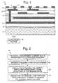
- Fig 1is a cross sectional side view showing fabrication of a flexible high density multilayer interconnect (HDMI structure 10 formed using methods 20 in accordance with the principles of the present invention.
- the flexible HDMI structure 10is fabricated on a relatively large carrier 11, typically having dimensions on the order of two feet by two feet.
- the carrier 11comprises an ultraviolet transparent substrate or wafer, such as quartz, for example.
- the carrier 11has a release layer 12 formed or otherwise deposited thereon.
- a polyimide layeris deposited as the release layer 12.
- the flexible HDMI structure 10is comprised of a plurality of dielectric layers 15 having fine line metallization patterns 13 formed therethrough that terminate at bond pads 17 on one or more surfaces of the fabricated flexible HDMI structure 10 and at cooperative bond pads (not shown) that are connected to electronic components.
- each of the HDMI structures 10may comprise dielectric layers 15 comprising polyimide having aluminum fine line interconnects 13,16 and vias 14 formed therethrough that provide signal paths from the bond pads 17 disposed at the surface of the HDMI structure 10 to other bond pads that are connected to the electronic components.
- the plurality of HDMI structures 10are formed on the carrier 11 and release layer 12 using well-known MCM-D processing techniques. Processing that may be used to fabricate the HDMI structures 10 is described in U.S. Patent No. 5,034,091 , entitled “Method of Forming an Electrical Via Structure", and assigned to the assignee of the present invention.
- the release layer 12is processed to release or remove one or more fabricated HDMI interconnect structures 10 from the carrier 11. More specifically, once the plurality of HDMI structures 10 are formed, a short wavelength ultraviolet radiation source 18, which is programmable and controlled, is used to release individual ones of the HDMI structures 10. A programmable pick and place machine may be used to physically remove the HDMI structures 10 once they are released from the carrier 11.
- a flood beam ultraviolet radiation source 18may be used to release many or all of the HDMI structures 10 from the ultraviolet transparent substrate or carrier 11.
- the ultraviolet radiation source 18is caused to radiate ultraviolet radiation through the ultraviolet transparent carrier 11 and onto the release layer 12.
- an ultraviolet lasermay be used to selectively irradiate one of the HDMI structures 10 to release it from the release layer 12.
- the ultraviolet radiation (photons) from the ultraviolet radiation source 18interacts with the polyimide release layer 12 adjacent to the carrier 11 and ruptures or otherwise breaks the adhesive bond therebetween. This permits the HDMI structures 10 to be lifted off of the carrier 11 using the programmable pick and place machine or other tool, for example. Multiple HDMI structures 10 may be released from the carrier 11 using a wide area ultraviolet radiation source 18 in a similar manner.
- the present inventionachieves or exceeds currently producible fine line density and stability demands for flexible interconnects.
- the present inventionuses improved materials such as polyimide and aluminum to form the HDMI interconnect structures 10 and an improved manufacturing technique for making and releasing the HDMI structures 10 from the carrier 11 either individually or in mass.
- the present inventionallows the formation of all aluminum (radiation hardened) flexible HDMI structures 10 that may be used in space and other military electronic systems.
- the present inventionallows high density unimetallization (aluminum or copper) to be used to form the fine line metallized interconnects 13,16 and vias 14, which is ideal for power devices.
- the present inventionalso provides for a 95% reduction in weight compared to presently available flexible HDMI substrates of the same size that are currently used in electronics designed for military aircraft and space systems developed by the assignee of the present invention.
- the present inventionhas diverse commercial applications where fine pitch interconnects are needed, such as for three-dimensional flexible cables, and membrane IC test boards, and the like, that are to be used at relatively high temperatures, on the order of 165 degrees Celsius.
- FIG. 2shows a flow diagram illustrating method 20 in accordance with the present invention for forming flexible HDMI structures 10 on a carrier 11 and subsequently releasing the HDMI interconnect 35 structures 10 either individually or in total from the carrier 11.
- the present method 20is as follows.
- a method 20comprises the steps of providing 21 a transparent carrier 11 that is transparent to ultraviolet radiation, forming 22 a release layer 12 on the transparent carrier 11, fabricating 23 flexible high density multilayer interconnect (HDMI) structures 10 on the release layer 12, and processing 24 the release layer 12 to release the flexible HDMI structures 10 from the rigid carrier 11, such as by irradiating the release layer 12 through the transparent carrier 11 using an ultraviolet radiation source 18.
- a transparent carrier 11that is transparent to ultraviolet radiation
- a release layer 12on the transparent carrier 11
- HDMIflexible high density multilayer interconnect
Landscapes
- Engineering & Computer Science (AREA)
- Manufacturing & Machinery (AREA)
- Microelectronics & Electronic Packaging (AREA)
- Physics & Mathematics (AREA)
- Condensed Matter Physics & Semiconductors (AREA)
- General Physics & Mathematics (AREA)
- Computer Hardware Design (AREA)
- Power Engineering (AREA)
- Ceramic Engineering (AREA)
- Production Of Multi-Layered Print Wiring Board (AREA)
- Laminated Bodies (AREA)
Description
- The present invention relates generally to processing methods for forming high density multichip interconnect (HDMI) structures, and more particularly, to methods of forming flexible HDMI decals comprising flexible fine line interconnect structures.
- Conventional flexible interconnect manufacturing techniques are limited in terms of the available materials that may be used and the line densities that may be achieved. The latest generation integrated circuits (IC), liquid crystal displays, three dimensional electronic structures, and infrared detectors impose a greater demand for higher density interconnects with improved thermal, environmental stability and lower cost.
- Presently available state of the art flexible interconnect cables are fabricated in a non-integrated circuit fabrication environment that limits their fine line density. Generally, conventional flexible connection cables are formed by applying an adhesive layer between each of the multiple layers to hold them together. This limits the operating temperature and the thermal stability of the fabricated flexible interconnect cables. Interconnect metallization in the conventional flexible interconnection cables is typically formed using copper which is not a radiation, hardened material and is not optimal for using power and radiation-hardened space and military applications.
US 5,262,351 discloses a method of producing a multi-layer polymer-metal system to interconnect integrated circuits which allows two-dimensional electrical and/or optical connections between components, in which a first layer of polymer is deposited on a rigid substrate such that the layer can be separated from the substrate, in which a multi-layer interconnection system is then produced on this first layer using industrial methods and in which the rigid substrate is removed after installation and connection of the integrated circuit.US 5,192,716 discloses a semiconductor structure which is provided by forming a thin film multi-layer wiring decal on a support substrate and aligning and attaching one or more integrated chips to the decall. A support ring is attached to the decal surrounding the aligned and attached integrated substrate, and the support substrate is removed by using etching techniques.- It is an objective of the present invention to provide for methods of forming flexible HDMI decals comprising flexible fine line HDMI interconnect structures.
- To meet the above and other objectives, the present invention provides for methods of forming a plurality of high density multilayer interconnect (HDMI) structures on a relatively large carrier or substrate and subsequently releasing one or more of the HDMI interconnect structures to provide useable flexible interconnects or decals. In general, a carrier is provided and a release layer is formed on the carrier. A flexible high density multilayer interconnect (HDMI) structure is then fabricated on the release layer. Finally, the release layer is processed to release and remove one or more flexible HDMI structures from the carrier.
- The carrier comprises a rigid ultraviolet transparent substrate or wafer. The release layer is formed on the ultraviolet transparent carrier that is subsequently processed to release the HDMI interconnect structures from the carrier. The release layer may comprise a polyimide layer.
- The plurality of HDMI structures are formed on the carrier and release layer using well-known MCM-D processing techniques. Each of the HDMI structures comprise layers of polyimide having aluminum or copper fine line interconnects and vias formed therethrough that provide signal paths from bond pads disposed at a surface of the HDMI structure to other bond pads that are used to connect to electronic components.
- Once the plurality of HDMI structures are formed on the release layer, a short wavelength ultraviolet radiation source, which may be programmable and controllable, is used to release individual ones of the HDMI structures. Alternatively, a flood beam ultraviolet radiation source may be used to release many or all of the HDMI structures from the ultraviolet transparent carrier. The ultraviolet source is caused to radiate ultraviolet radiation through the transparent carrier and onto the release layer disposed between the fabricated HDMI structures and the carrier. For example, a controllable ultraviolet laser may be used to selectively irradiate each of the HDMI structures, in conjunction with a programmable pick and place machine, for example, to release and remove it from the release layer and carrier.
- To achieve the removal of HDMI structures, ultraviolet radiation (photons) from the ultraviolet source interacts with the polyimide layer adjacent to the carrier and ruptures or otherwise breaks the adhesive bond therebetween. This permits the HDMI structures to be lifted off of the carrier using the programmable pick and place machine or other tool. Multiple HDMI structures may be released from the carrier using the wide area ultraviolet source in a similar manner.
- The present invention achieves or exceeds currently producible fine line density and stability demands for flexible interconnects by using improved materials (polyimide and aluminum or copper) and an improved manufacturing technique for making fine line flexible interconnect structures by fabricating them on the ultraviolet transparent carrier and releasing them by irradiating them individually or in mass using ultraviolet radiation. The present invention allows the formation of all aluminum (radiation hardened) flexible high density multilayer interconnect (HDMI) structures that may be used in space and other military electronic systems.
- The present invention allows high density unimetallization (aluminum) to be used to form the fine line metallized conductors, which is ideal for power devices. The present invention also provides for a 95% reduction in weight compared to presently available HDMI substrates used in electronics designed for military aircraft and space systems developed by the assignee of the present invention. The present invention has diverse commercial applications where fine pitch interconnects are needed, such as for three-dimensional flexible cables, and membrane IC test boards, and the like, that are to be used at relatively high temperatures, on the order of 165 degrees Celsius.
- The various features and advantages of the present invention may be more readily understood with reference to the following detailed description taken in conjunction with the accompanying drawings, wherein like reference numerals designate like structural elements, and in which:
Fig 1 is a cross sectional side view showing fabrication of a flexible high density multilayer interconnect structure formed using methods in accordance with the principles of the present invention; andFig. 2 shows a flow diagram illustrating details of the present method.- Referring to the drawing figures,
Fig 1 is a cross sectional side view showing fabrication of a flexible high density multilayer interconnect (HDMI structure 10 formed usingmethods 20 in accordance with the principles of the present invention. Theflexible HDMI structure 10 is fabricated on a relativelylarge carrier 11, typically having dimensions on the order of two feet by two feet. Thecarrier 11 comprises an ultraviolet transparent substrate or wafer, such as quartz, for example. - The
carrier 11 has arelease layer 12 formed or otherwise deposited thereon. A polyimide layer is deposited as therelease layer 12. - The
flexible HDMI structure 10 is comprised of a plurality ofdielectric layers 15 having fineline metallization patterns 13 formed therethrough that terminate atbond pads 17 on one or more surfaces of the fabricatedflexible HDMI structure 10 and at cooperative bond pads (not shown) that are connected to electronic components. For example, each of theHDMI structures 10 may comprisedielectric layers 15 comprising polyimide having aluminumfine line interconnects vias 14 formed therethrough that provide signal paths from thebond pads 17 disposed at the surface of theHDMI structure 10 to other bond pads that are connected to the electronic components. The plurality ofHDMI structures 10 are formed on thecarrier 11 andrelease layer 12 using well-known MCM-D processing techniques. Processing that may be used to fabricate theHDMI structures 10 is described inU.S. Patent No. 5,034,091 , entitled "Method of Forming an Electrical Via Structure", and assigned to the assignee of the present invention. - The
release layer 12 is processed to release or remove one or more fabricatedHDMI interconnect structures 10 from thecarrier 11. More specifically, once the plurality ofHDMI structures 10 are formed, a short wavelengthultraviolet radiation source 18, which is programmable and controlled, is used to release individual ones of theHDMI structures 10. A programmable pick and place machine may be used to physically remove theHDMI structures 10 once they are released from thecarrier 11. - Alternatively, a flood beam
ultraviolet radiation source 18 may be used to release many or all of theHDMI structures 10 from the ultraviolet transparent substrate orcarrier 11. Theultraviolet radiation source 18 is caused to radiate ultraviolet radiation through the ultraviolettransparent carrier 11 and onto therelease layer 12. For example, an ultraviolet laser may be used to selectively irradiate one of theHDMI structures 10 to release it from therelease layer 12. - The ultraviolet radiation (photons) from the
ultraviolet radiation source 18 interacts with thepolyimide release layer 12 adjacent to thecarrier 11 and ruptures or otherwise breaks the adhesive bond therebetween. This permits theHDMI structures 10 to be lifted off of thecarrier 11 using the programmable pick and place machine or other tool, for example.Multiple HDMI structures 10 may be released from thecarrier 11 using a wide areaultraviolet radiation source 18 in a similar manner. - The present invention achieves or exceeds currently producible fine line density and stability demands for flexible interconnects. The present invention uses improved materials such as polyimide and aluminum to form the
HDMI interconnect structures 10 and an improved manufacturing technique for making and releasing theHDMI structures 10 from thecarrier 11 either individually or in mass. The present invention allows the formation of all aluminum (radiation hardened)flexible HDMI structures 10 that may be used in space and other military electronic systems. - The present invention allows high density unimetallization (aluminum or copper) to be used to form the fine line
metallized interconnects vias 14, which is ideal for power devices. The present invention also provides for a 95% reduction in weight compared to presently available flexible HDMI substrates of the same size that are currently used in electronics designed for military aircraft and space systems developed by the assignee of the present invention. The present invention has diverse commercial applications where fine pitch interconnects are needed, such as for three-dimensional flexible cables, and membrane IC test boards, and the like, that are to be used at relatively high temperatures, on the order of 165 degrees Celsius. - For the purposes of completeness,
Fig. 2 shows a flowdiagram illustrating method 20 in accordance with the present invention for formingflexible HDMI structures 10 on acarrier 11 and subsequently releasing the HDMI interconnect 35structures 10 either individually or in total from thecarrier 11. Thepresent method 20 is as follows. - Referring to
Fig. 2 , amethod 20 comprises the steps of providing 21 atransparent carrier 11 that is transparent to ultraviolet radiation, forming 22 arelease layer 12 on thetransparent carrier 11, fabricating 23 flexible high density multilayer interconnect (HDMI)structures 10 on therelease layer 12, and processing 24 therelease layer 12 to release theflexible HDMI structures 10 from therigid carrier 11, such as by irradiating therelease layer 12 through thetransparent carrier 11 using anultraviolet radiation source 18. - Thus, a method for forming flexible HDMI decals comprising flexible fine line interconnect structures has been disclosed. It is to be understood that the described embodiments are merely illustrative of some of the many specific embodiments which represent applications of the principles of the present invention. Clearly, numerous and varied other arrangements may be readily devised by those skilled in the art without departing from the scope of the invention.
Claims (5)
- A method of fabricating flexible high density multilayer interconnect (HDMI) structures (10),characterized by the steps of:- providing (21) a carrier (11) transparent to ultraviolet radiation;- forming (22) a release layer (12) on said carrier (11);- fabricating (23) a flexible HDMI structure (10) on said release layer (12); and- processing (24) said release layer (12) to release and remove said flexible HDMI structure (10) from said carrier (11), comprising irradiating said release layer (12) through said carrier (11) with ultraviolet radiation.
- The method of claim 1,characterized in that said step (21) of providing comprises providing a rigid carrier (11).
- The method of claim 2,characterized in that said carrier (11) is made of quartz.
- The method of any of claims 1 to 3,characterized in that said step (22) of forming includes forming said release layer (12) from polyimide.
- The method of any of claims 1 to 4,characterized by the further step of providing said HDMI structure (10) with dielectric layers (15) having metal fine line interconnects (13, 16) and vias (14) formed therethrough that provide signal paths from bond pads (17) disposed at the surface of said HDMI structure (10) to associated electronic components.
Applications Claiming Priority (2)
| Application Number | Priority Date | Filing Date | Title |
|---|---|---|---|
| US62995696A | 1996-04-08 | 1996-04-08 | |
| US629956 | 1996-04-08 |
Publications (3)
| Publication Number | Publication Date |
|---|---|
| EP0801423A2 EP0801423A2 (en) | 1997-10-15 |
| EP0801423A3 EP0801423A3 (en) | 1998-12-09 |
| EP0801423B1true EP0801423B1 (en) | 2008-09-17 |
Family
ID=24525169
Family Applications (1)
| Application Number | Title | Priority Date | Filing Date |
|---|---|---|---|
| EP19970105477Expired - LifetimeEP0801423B1 (en) | 1996-04-08 | 1997-04-02 | Hdmi decal and fine line flexible interconnect forming methods |
Country Status (3)
| Country | Link |
|---|---|
| EP (1) | EP0801423B1 (en) |
| JP (1) | JP2918863B2 (en) |
| DE (1) | DE69738994D1 (en) |
Families Citing this family (10)
| Publication number | Priority date | Publication date | Assignee | Title |
|---|---|---|---|---|
| US6018463A (en)* | 1997-08-22 | 2000-01-25 | Raytheon Company | Large non-hermetic multichip module package |
| JP2001267747A (en)* | 2000-03-22 | 2001-09-28 | Nitto Denko Corp | Method for manufacturing multilayer circuit board |
| US6670921B2 (en) | 2001-07-13 | 2003-12-30 | Hrl Laboratories, Llc | Low-cost HDMI-D packaging technique for integrating an efficient reconfigurable antenna array with RF MEMS switches and a high impedance surface |
| US20030113947A1 (en)* | 2001-12-19 | 2003-06-19 | Vandentop Gilroy J. | Electrical/optical integration scheme using direct copper bonding |
| JP3811680B2 (en)* | 2003-01-29 | 2006-08-23 | 富士通株式会社 | Wiring board manufacturing method |
| US7951687B2 (en) | 2003-04-02 | 2011-05-31 | Polymer Vision Limited | Method of manufacturing a flexible electronic device and flexible device |
| JP4841806B2 (en)* | 2004-02-02 | 2011-12-21 | 新光電気工業株式会社 | Capacitor device, semiconductor device including the same, and method of manufacturing capacitor device |
| GB0414487D0 (en)* | 2004-06-29 | 2004-07-28 | Xaar Technology Ltd | Manufacture of electronic devices |
| DE202014103821U1 (en) | 2014-07-09 | 2014-09-09 | Carmen Diegel | Flexible electrical conductor structure |
| CN114678163A (en)* | 2021-12-15 | 2022-06-28 | 上海脑虎科技有限公司 | Structure, preparation method and brain electrode device of a flexible connecting cable |
Family Cites Families (4)
| Publication number | Priority date | Publication date | Assignee | Title |
|---|---|---|---|---|
| US4306925A (en)* | 1977-01-11 | 1981-12-22 | Pactel Corporation | Method of manufacturing high density printed circuit |
| US5192716A (en)* | 1989-01-25 | 1993-03-09 | Polylithics, Inc. | Method of making a extended integration semiconductor structure |
| US4980034A (en)* | 1989-04-04 | 1990-12-25 | Massachusetts Institute Of Technology | High-density, multi-level interconnects, flex circuits, and tape for TAB |
| FR2666173A1 (en)* | 1990-08-21 | 1992-02-28 | Thomson Csf | HYBRID INTERCONNECTION STRUCTURE FOR INTEGRATED CIRCUITS AND MANUFACTURING METHOD. |
- 1997
- 1997-04-02DEDE69738994Tpatent/DE69738994D1/ennot_activeExpired - Lifetime
- 1997-04-02EPEP19970105477patent/EP0801423B1/ennot_activeExpired - Lifetime
- 1997-04-08JPJP8956497Apatent/JP2918863B2/ennot_activeExpired - Lifetime
Also Published As
| Publication number | Publication date |
|---|---|
| DE69738994D1 (en) | 2008-10-30 |
| EP0801423A3 (en) | 1998-12-09 |
| JPH1075055A (en) | 1998-03-17 |
| JP2918863B2 (en) | 1999-07-12 |
| EP0801423A2 (en) | 1997-10-15 |
Similar Documents
| Publication | Publication Date | Title |
|---|---|---|
| US5691245A (en) | Methods of forming two-sided HDMI interconnect structures | |
| US5998291A (en) | Attachment method for assembly of high density multiple interconnect structures | |
| US5373627A (en) | Method of forming multi-chip module with high density interconnections | |
| US5817541A (en) | Methods of fabricating an HDMI decal chip scale package | |
| US9691698B2 (en) | Method of transferring and electrically joining a high density multilevel thin film to a circuitized and flexible organic substrate and associated devices | |
| CN102479724B (en) | A method of manufacturing a heat dissipation gain type stacked semiconductor component | |
| US5527741A (en) | Fabrication and structures of circuit modules with flexible interconnect layers | |
| US7348261B2 (en) | Wafer scale thin film package | |
| US5280139A (en) | Selectively releasing conductive runner and substrate assembly | |
| US7408258B2 (en) | Interconnection circuit and electronic module utilizing same | |
| EP0450950B1 (en) | A flexible high density interconnect structure | |
| US5778529A (en) | Method of making a multichip module substrate | |
| JPH06350020A (en) | Multichip integrated circuit module and its manufacture | |
| EP0801423B1 (en) | Hdmi decal and fine line flexible interconnect forming methods | |
| KR20130143536A (en) | Multilayer electronic structure with integral metal core | |
| KR102719490B1 (en) | Packaging structure and manufacturing method thereof | |
| KR20010088866A (en) | Deposited thin build-up layer dimensions as a method of relieving stress in high density interconnect printed wiring board substrates | |
| EP1026929A2 (en) | Elemental piece of flexible printed wiring board and flexible printed wiring board | |
| CN116033645A (en) | Coreless component carrier and method for producing a coreless component carrier | |
| CN111341750B (en) | Component carrier comprising an electrically conductive base structure and method of manufacture | |
| US10897823B2 (en) | Circuit board, package structure and method of manufacturing the same | |
| EP4152388A1 (en) | Electronic package with components mounted at two sides of a layer stack | |
| Blum et al. | Multichip module substrates | |
| WO1992017045A1 (en) | Multi-level/multi-layered hybrid package | |
| JPH05198627A (en) | Hybrid module and manufacture thereof |
Legal Events
| Date | Code | Title | Description |
|---|---|---|---|
| PUAI | Public reference made under article 153(3) epc to a published international application that has entered the european phase | Free format text:ORIGINAL CODE: 0009012 | |
| AK | Designated contracting states | Kind code of ref document:A2 Designated state(s):DE FR GB | |
| RAP1 | Party data changed (applicant data changed or rights of an application transferred) | Owner name:RAYTHEON COMPANY (A DELAWARE CORPORATION) | |
| PUAL | Search report despatched | Free format text:ORIGINAL CODE: 0009013 | |
| RAP1 | Party data changed (applicant data changed or rights of an application transferred) | Owner name:RAYTHEON COMPANY | |
| AK | Designated contracting states | Kind code of ref document:A3 Designated state(s):DE FR GB | |
| 17P | Request for examination filed | Effective date:19990605 | |
| GRAP | Despatch of communication of intention to grant a patent | Free format text:ORIGINAL CODE: EPIDOSNIGR1 | |
| GRAS | Grant fee paid | Free format text:ORIGINAL CODE: EPIDOSNIGR3 | |
| GRAA | (expected) grant | Free format text:ORIGINAL CODE: 0009210 | |
| AK | Designated contracting states | Kind code of ref document:B1 Designated state(s):DE FR GB | |
| REG | Reference to a national code | Ref country code:GB Ref legal event code:FG4D | |
| REF | Corresponds to: | Ref document number:69738994 Country of ref document:DE Date of ref document:20081030 Kind code of ref document:P | |
| PLBE | No opposition filed within time limit | Free format text:ORIGINAL CODE: 0009261 | |
| STAA | Information on the status of an ep patent application or granted ep patent | Free format text:STATUS: NO OPPOSITION FILED WITHIN TIME LIMIT | |
| 26N | No opposition filed | Effective date:20090618 | |
| REG | Reference to a national code | Ref country code:FR Ref legal event code:PLFP Year of fee payment:20 | |
| PGFP | Annual fee paid to national office [announced via postgrant information from national office to epo] | Ref country code:GB Payment date:20160330 Year of fee payment:20 Ref country code:FR Payment date:20160309 Year of fee payment:20 | |
| PGFP | Annual fee paid to national office [announced via postgrant information from national office to epo] | Ref country code:DE Payment date:20160330 Year of fee payment:20 | |
| REG | Reference to a national code | Ref country code:DE Ref legal event code:R071 Ref document number:69738994 Country of ref document:DE | |
| REG | Reference to a national code | Ref country code:GB Ref legal event code:PE20 Expiry date:20170401 | |
| PG25 | Lapsed in a contracting state [announced via postgrant information from national office to epo] | Ref country code:GB Free format text:LAPSE BECAUSE OF EXPIRATION OF PROTECTION Effective date:20170401 |