EP0798744B1 - Timing characterization circuit and method for memory devices - Google Patents
Timing characterization circuit and method for memory devicesDownload PDFInfo
- Publication number
- EP0798744B1 EP0798744B1EP96830176AEP96830176AEP0798744B1EP 0798744 B1EP0798744 B1EP 0798744B1EP 96830176 AEP96830176 AEP 96830176AEP 96830176 AEP96830176 AEP 96830176AEP 0798744 B1EP0798744 B1EP 0798744B1
- Authority
- EP
- European Patent Office
- Prior art keywords
- signal
- reset
- enabling
- receiving
- circuit
- Prior art date
- Legal status (The legal status is an assumption and is not a legal conclusion. Google has not performed a legal analysis and makes no representation as to the accuracy of the status listed.)
- Expired - Lifetime
Links
- 238000012512characterization methodMethods0.000titleclaimsdescription21
- 238000000034methodMethods0.000titleclaimsdescription8
- 230000001934delayEffects0.000claimsdescription2
- 238000011156evaluationMethods0.000claimsdescription2
- 238000010586diagramMethods0.000description3
- 238000011835investigationMethods0.000description2
- 230000007704transitionEffects0.000description2
- 239000003990capacitorSubstances0.000description1
- 238000013461designMethods0.000description1
- 230000006870functionEffects0.000description1
- 230000003071parasitic effectEffects0.000description1
- 230000008569processEffects0.000description1
- 230000004044responseEffects0.000description1
- 238000012360testing methodMethods0.000description1
Images

Classifications
- G—PHYSICS
- G11—INFORMATION STORAGE
- G11C—STATIC STORES
- G11C16/00—Erasable programmable read-only memories
- G11C16/02—Erasable programmable read-only memories electrically programmable
- G11C16/06—Auxiliary circuits, e.g. for writing into memory
- G11C16/26—Sensing or reading circuits; Data output circuits
- G—PHYSICS
- G11—INFORMATION STORAGE
- G11C—STATIC STORES
- G11C16/00—Erasable programmable read-only memories
- G11C16/02—Erasable programmable read-only memories electrically programmable
- G11C16/06—Auxiliary circuits, e.g. for writing into memory
- G11C16/32—Timing circuits
Definitions
- the present inventionrelates to a timing characterization circuit and method for memory devices.
- a memorye.g. a nonvolatile memory such as an EPROM, to which reference is made herein by way of example
- basic time eventssuch as the propagation or precharge intervals of basic lines (e.g. word lines, bit lines, redundancy) and the instant in which the data item in a given memory location is evaluated.
- timing characterization circuita memory device, and a timing characterization method as claimed respectively in Claims 1, 7 and 9.
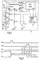
- the memory deviceis indicated as a whole by 1, and comprises a nonvolatile memory, such as an EPROM, of which are shown only the parts pertinent to the present invention.
- a nonvolatile memorysuch as an EPROM
- Memory device 1comprises a timing characterization circuit 2; a memory array 3 including a number of memory cells 4; a logic stage 5 incorporating all the other timing and control components of memory 1; an output buffer stage 6; a third-level circuit 7; and three contact pads 8, 9, 10.
- Characterization circuit 2presents a first input 13 connected to and supplied by third-level circuit 7 with a voltage level TLEV (for enabling the characterization step); a second input 14 supplied with signal OE (for controlling the characterization step); a third, fourth and fifth input 15, 16, 17 connected to and supplied respectively by logic stage 5 with signal ATD (indicating address transition at the start of the read step), signal CE (for enabling circuit 2), and RES (for resetting at the end of the read step); and an output 18 connected to logic stage 5 and supplying a precharge signal PCn.
- TLEVvoltage level
- OEfor controlling the characterization step
- a third, fourth and fifth input 15, 16, 17connected to and supplied respectively by logic stage 5 with signal ATD (indicating address transition at the start of the read step), signal CE (for enabling circuit 2), and RES (for resetting at the end of the read step)
- an output 18connected to logic stage 5 and supplying a precharge signal PCn.
- Third-level circuit 7(of a known type) comprises a number of diode-connected transistors 20 in series between contact pad 8 and a node 21 grounded via an NMOS transistor 22 having a gate terminal connected to supply line 23 at V DD .
- Node 21is also connected to input 13 of characterization circuit 2 via two inverters 24, 25 cascade connected to each other, so that, when a high voltage (e.g. of 8 to 12 V) is applied to pad 8, input 13 presents a third-level voltage (greater than V DD ).
- Pad 9(supplied externally with signal OEn) is connected to the input of an inverter 27, the output of which is connected both to input 14 of characterization circuit 2 and to one input of output buffer stage 6.
- Output buffer stage 6also has an input connected to memory array 3, and an output connected to pad 10, so as to receive the data read by memory array 3 and supply it externally of device 1 to pad 10 when enabled by signal OE, which provides for enabling/disabling output buffer stage 6 independently of the internal timing.
- Figure 1also shows the connection between the output 18 of circuit 2 and memory array 3, for supplying memory array 3 with signal PCn; and the connection between logic stage 5 and memory array 3, for supplying memory array 3 with an equalizing signal EQ used in known manner for reading memory cells 4.
- inputs 15 and 16are connected to respective gate terminals of two NMOS transistors 30, 31; transistor 31 has the source terminal grounded, and the drain terminal connected to the source terminal of transistor 30; and transistor 30 has the drain terminal connected to the input node 32 of a latch 33 presenting an output node 34 connected via an inverter 35 to output 18.
- Latch 33comprises two PMOS transistors 38, 39, and two NMOS transistors 40, 41. More specifically, PMOS transistors 38, 39 have the source terminals connected to supply line 23 at V DD , the gate terminals connected respectively to output node 34 and input node 32, and the drain terminals connected respectively to input node 32 and output node 34; and NMOS transistors 40, 41 have the source terminals grounded, the gate terminals connected respectively to output node 34 and input node 32, and the drain terminals connected respectively to input node 32 and output node 34.
- reset branch 43comprises an NMOS transistor 46 having the drain terminal connected to output node 34 of latch 33, the gate terminal connected to input 16 of circuit 2 via an inverter 47, and the source terminal grounded.
- Reset branch 44comprises two NMOS transistors 48, 49; transistor 48 has the drain terminal connected to output node 34 of latch 33, the gate terminal connected to input 14 of circuit 2, and the source terminal connected to the drain terminal of transistor 49; and transistor 49 has the gate terminal connected to a node 50, and the source terminal grounded.
- Reset branch 45comprises two NMOS transistors 52, 53; transistor 52 has the drain terminal connected to output node 34 of latch 33, the gate terminal connected to input 17 of circuit 2, and the source terminal connected to the drain terminal of transistor 53; and transistor 53 has the gate terminal connected to a node 55, and the source terminal grounded.
- inverters 56, 57, 58are cascade connected between input 13 of circuit 2 and node 55; and the output of inverter 57, between inverters 56 and 58, forms node 50.
- a capacitor 60is connected between output 18 of circuit 2 and ground.
- circuit 2 in Figure 1operates as follows.
- transistor 30Upon signal ATD switching to high, transistor 30 is turned on and grounds input 32 of latch 33; output 34 switches to high ( Figure 3); and, at the same time, logic stage 5, receiving signal PCn, switches signal EQ to high.
- the known circuit generating signal EQis not shown.
- Signal EQmay, for example, be generated quite simply from signal PCn by means of asymmetric inverters, i.e. presenting different switching times depending on the switching edge at the input, so that signal EQ switches to high when PCn switches to low, and switches to low with a predetermined delay in relation to low-to-high switching of PCn).
- stage 5At the end of the precharge step (to commence evaluation of the memorized data item), stage 5 generates a pulse in signal RES in known manner, which turns on transistor 52, enables reset branch 45, grounds output node 34, and switches latch 33, so that input node 32 switches to high, signal PCn switches back to high, and signal EQ also switches (continuous line plots in Figure 3).
- the above succession of eventsmay be modified to characterize the timing circuits of device 1 by means of a third-level signal TLEV (or appropriate code) for disabling reset branch 45 and enabling reset branch 44, which is controllable externally by signal OEn supplied to pad 9 ( Figure 1).
- TLEVor appropriate code
- a high voltage at pad 8switches signal TLEV and node 50 to high, and node 51 to low, so that branch 44 is enabled (even though it remains off, in the absence of signal OE), and branch 45 is disabled (transistor 53 off).
- circuit 2On receiving signal ATD, therefore, circuit 2 initially functions as described above, with latch 33 switching and PCn switching to low. In this case, however, the switching of signal RES is ineffective, and the reset condition and the switching of PCn and EQ are now controlled by OE, supplied externally, so as to shorten or lengthen the active state duration of signals PCn and EQ as shown by the dotted lines in Figure 3.
- the findingsmay then be used to modify and regulate the internal circuits of stage 5 to generate, among other things, the instant at which the RES signal is switched, and the disabling switch delay of signal EQ.
- the characterizations so obtainedmay be used to regulate the timing circuit described in EP-A-O 668 592, for switching the memory elements governing fast or slow read timing conditions.
- the same modemay also be applied for investigation purposes, for determining any discrepancy between process parameters and nominal values (e.g. resistance of propagation lines, increase in parasitic capacitance, characteristics of the device 1 components and stages) or for characterizing the functionality, criticality and limitations of the various components and stages of device 1 to determine its marginality and reliability.
- process parameters and nominal valuese.g. resistance of propagation lines, increase in parasitic capacitance, characteristics of the device 1 components and stages
- circuit and method describedprovide for perfecting the succession of read events of a memory device on the basis of real performance and contingent local situations by providing for flexible timing basically controlled externally; they represent a convenient means of investigation and characterizing propagation in the event of malfunctioning; and, finally, the circuit itself is straightforward, easy to integrate, compact and reliable.
- the characterization stepmay be enabled by means of an appropriate code or signal, instead of a third level, as described.
Landscapes
- Read Only Memory (AREA)
- Dram (AREA)
Description
Claims (11)
- A timing characterization circuit (2) for amemory device (1), comprising an enabling input (15)receiving an enabling signal (ATD); a reset input (17)receiving a reset signal (RES); an output (18); andtiming source means (33) connected to said enabling andreset inputs and to said output, and in turn comprisinga first reset circuit (45) for generating an operatingstep enabling signal (PCn); said operating step enablingsignal presenting a first switching edge on receivingsaid enabling signal (ATD), and a second switching edgeon receiving said reset signal (RES);characterized by acontrol input (14) receiving an external timing controlsignal (OE); and a second reset circuit (44) connectedto said control input (14) and determining a thirdswitching edge of said operating step enabling signal(PCn) on receiving said external timing control signal(OE).
- A circuit as claimed in Claim 1,characterizedby a control input (13) receiving a timing mode signal(TLEV); and disabling means (49, 53, 58) controlled bysaid timing mode signal and connected to said first andsecond reset circuits (45, 44) to selectively andalternately disable said first and second resetcircuits.
- A circuit as claimed in Claim 2,characterizedin that said timing mode signal (TLEV) comprises a third level.
- A circuit as claimed in Claim 3,characterizedin that said timing mode signal (TLEV) comprises a codedsignal.
- A circuit as claimed in any one of theforegoing Claims,characterized in that said timingsource means comprises a memory element (33) connectedbetween a first and a second line at a first (VDD) and asecond reference potential respectively, and having aninput (32) connected to said enabling input, and anoutput (34) connected to said output (18) of saidcharacterization circuit (2), said memory element (33)bringing its own said output (34) to said firstreference potential on receiving said enabling signal(ATD) ; andin that said first and second reset circuits(45, 44) are connected to and bring said output (34) ofsaid memory element (33) to said second referencepotential on receiving said reset signal (RES) and saidexternal timing control signal (OE) respectively.
- A circuit as claimed in Claim 5,characterizedin that said memory element is a latch (33); andin thatsaid first and second reset circuits (45, 44) eachcomprise controlled switching means (52, 48) interposedbetween said output (34) of said memory element (33) andsaid second reference potential line, and respectivelyreceiving said reset signal (RES) and said externaltiming control signal (OE).
- A memory device (1) comprising a data output (10); a memory array (3); timing means (2, 5) forgenerating operating step control signals and connectedto said memory array; and output means (6) connectedbetween said memory array and said data output;characterized by a timing characterization circuit (2)as claimed in any one of the foregoing Claims from 1 to6.
- A memory device as claimed in Claim 7,characterized by a characterization control input (8)receiving an external characterization control signaland connected to said first and second reset circuits(45, 44) for selective enabling thereof; and acharacterization control input (9) receiving saidexternal timing control signal (OE) and connected tosaid second reset circuit (44) and to said output means(6).
- A timing characterization method for a memorydevice, comprising the steps of: generating firstswitching edges of operating step enabling signals (PCn,EQ) of said memory device; generating a reset signal(RES); and enabling first reset circuits determiningsecond switching edges of said operating step enablingsignals on receiving said reset signal;characterized bythe steps of generating external timing control signals(OE) with a predetermined delay in relation to saidfirst switching edges; and enabling second resetcircuits determining third switching edges of saidoperating step enabling signals on receiving said external timing control signals.
- A method as claimed in Claim 9,characterizedin that said step of generating external timing controlsignals (OE) is preceded by the step of disabling saidfirst reset circuits.
- A method as claimed in Claim 10,characterizedby the further steps of: evaluating said memory device;repeating, with different delays, said disabling step,said step of generating external timing control signals,and said step of enabling second reset circuits; anddetermining optimum delay times on the basis of saidevaluation step.
Priority Applications (3)
| Application Number | Priority Date | Filing Date | Title |
|---|---|---|---|
| DE69630943TDE69630943D1 (en) | 1996-03-29 | 1996-03-29 | Time characterization circuit and method for storage systems |
| EP96830176AEP0798744B1 (en) | 1996-03-29 | 1996-03-29 | Timing characterization circuit and method for memory devices |
| US08/825,138US5886945A (en) | 1996-03-29 | 1997-03-28 | Circuit and method to adjust memory timing |
Applications Claiming Priority (1)
| Application Number | Priority Date | Filing Date | Title |
|---|---|---|---|
| EP96830176AEP0798744B1 (en) | 1996-03-29 | 1996-03-29 | Timing characterization circuit and method for memory devices |
Publications (2)
| Publication Number | Publication Date |
|---|---|
| EP0798744A1 EP0798744A1 (en) | 1997-10-01 |
| EP0798744B1true EP0798744B1 (en) | 2003-12-03 |
Family
ID=8225862
Family Applications (1)
| Application Number | Title | Priority Date | Filing Date |
|---|---|---|---|
| EP96830176AExpired - LifetimeEP0798744B1 (en) | 1996-03-29 | 1996-03-29 | Timing characterization circuit and method for memory devices |
Country Status (3)
| Country | Link |
|---|---|
| US (1) | US5886945A (en) |
| EP (1) | EP0798744B1 (en) |
| DE (1) | DE69630943D1 (en) |
Families Citing this family (3)
| Publication number | Priority date | Publication date | Assignee | Title |
|---|---|---|---|---|
| JP5034233B2 (en)* | 2005-12-28 | 2012-09-26 | 富士通株式会社 | Address decoder, storage device, processing device, and address decoding method in storage device |
| KR100735024B1 (en)* | 2005-12-29 | 2007-07-03 | 삼성전자주식회사 | Address Translator and Semiconductor Memory Device of Semiconductor Device |
| US8510598B2 (en)* | 2010-03-29 | 2013-08-13 | Dot Hill Systems Corporation | Buffer management method and apparatus for power reduction during flush operation |
Family Cites Families (7)
| Publication number | Priority date | Publication date | Assignee | Title |
|---|---|---|---|---|
| US4425633A (en)* | 1980-10-06 | 1984-01-10 | Mostek Corporation | Variable delay circuit for emulating word line delay |
| US4575812A (en)* | 1984-05-31 | 1986-03-11 | Motorola, Inc. | X×Y Bit array multiplier/accumulator circuit |
| US4687951A (en)* | 1984-10-29 | 1987-08-18 | Texas Instruments Incorporated | Fuse link for varying chip operating parameters |
| JP2803466B2 (en)* | 1992-04-28 | 1998-09-24 | 日本電気株式会社 | Relief method for semiconductor memory device |
| US5452311A (en)* | 1992-10-30 | 1995-09-19 | Intel Corporation | Method and apparatus to improve read reliability in semiconductor memories |
| DE69424860T2 (en)* | 1994-02-18 | 2000-11-09 | Stmicroelectronics S.R.L., Agrate Brianza | Method and circuit for generating a charging signal for non-volatile memories |
| US5487038A (en)* | 1994-08-15 | 1996-01-23 | Creative Integrated Systems, Inc. | Method for read cycle interrupts in a dynamic read-only memory |
- 1996
- 1996-03-29EPEP96830176Apatent/EP0798744B1/ennot_activeExpired - Lifetime
- 1996-03-29DEDE69630943Tpatent/DE69630943D1/ennot_activeExpired - Lifetime
- 1997
- 1997-03-28USUS08/825,138patent/US5886945A/ennot_activeExpired - Lifetime
Also Published As
| Publication number | Publication date |
|---|---|
| EP0798744A1 (en) | 1997-10-01 |
| US5886945A (en) | 1999-03-23 |
| DE69630943D1 (en) | 2004-01-15 |
Similar Documents
| Publication | Publication Date | Title |
|---|---|---|
| US5841827A (en) | Timer circuit with programmable decode circuitry | |
| US6522193B2 (en) | Internal voltage generator for semiconductor memory device | |
| US5341033A (en) | Input buffer circuit with deglitch method and apparatus | |
| US20060198231A1 (en) | Pulse controlled word line driver | |
| US6269031B1 (en) | Semiconductor memory device | |
| EP1324347B1 (en) | A circuit for controlling a reference node in a sense amplifier | |
| EP0814481B1 (en) | Low-supply-voltage nonvolatile memory device with voltage boosting | |
| US7884647B2 (en) | Output driver | |
| US6324112B1 (en) | Reading device and method for integrated circuit memory | |
| US5907514A (en) | Circuit and method for controlling a redundant memory cell in an integrated memory circuit | |
| US6020775A (en) | Adjustable timer circuit | |
| EP0798744B1 (en) | Timing characterization circuit and method for memory devices | |
| JPH0512898A (en) | Semiconductor integrated circuit device | |
| US6480430B2 (en) | Semiconductor device making reliable initial setting | |
| KR100186277B1 (en) | Semiconductor memory device with a decoding peropheral circuit for improving the operation frequency | |
| US7504864B2 (en) | Method for controlling the evaluation time of a state machine | |
| US6288594B1 (en) | Monolithically integrated selector for electrically programmable memory cell devices | |
| JPH10255472A (en) | Method and circuit for generating synchronous atd signal | |
| US5963077A (en) | Auto mode selector | |
| KR940002272B1 (en) | Semiconductor Memory Device with Redundancy Function | |
| JPH1064270A (en) | Semiconductor memory element with grounding noise separation function | |
| EP0668591A1 (en) | Read timing method and circuit for nonvolatile memories | |
| US6977862B2 (en) | Address decoding circuit and method for addressing a regular memory area and a redundant memory area in a memory circuit | |
| US5905678A (en) | Control circuit of an output buffer | |
| US6169423B1 (en) | Method and circuit for regulating the length of an ATD pulse signal |
Legal Events
| Date | Code | Title | Description |
|---|---|---|---|
| PUAI | Public reference made under article 153(3) epc to a published international application that has entered the european phase | Free format text:ORIGINAL CODE: 0009012 | |
| AK | Designated contracting states | Kind code of ref document:A1 Designated state(s):DE FR GB IT | |
| 17P | Request for examination filed | Effective date:19971210 | |
| RAP3 | Party data changed (applicant data changed or rights of an application transferred) | Owner name:STMICROELECTRONICS S.R.L. | |
| GRAH | Despatch of communication of intention to grant a patent | Free format text:ORIGINAL CODE: EPIDOS IGRA | |
| GRAS | Grant fee paid | Free format text:ORIGINAL CODE: EPIDOSNIGR3 | |
| GRAA | (expected) grant | Free format text:ORIGINAL CODE: 0009210 | |
| AK | Designated contracting states | Kind code of ref document:B1 Designated state(s):DE FR GB IT | |
| PG25 | Lapsed in a contracting state [announced via postgrant information from national office to epo] | Ref country code:FR Free format text:LAPSE BECAUSE OF FAILURE TO SUBMIT A TRANSLATION OF THE DESCRIPTION OR TO PAY THE FEE WITHIN THE PRESCRIBED TIME-LIMIT Effective date:20031203 | |
| REG | Reference to a national code | Ref country code:GB Ref legal event code:FG4D | |
| REF | Corresponds to: | Ref document number:69630943 Country of ref document:DE Date of ref document:20040115 Kind code of ref document:P | |
| PG25 | Lapsed in a contracting state [announced via postgrant information from national office to epo] | Ref country code:DE Free format text:LAPSE BECAUSE OF FAILURE TO SUBMIT A TRANSLATION OF THE DESCRIPTION OR TO PAY THE FEE WITHIN THE PRESCRIBED TIME-LIMIT Effective date:20040304 | |
| PLBE | No opposition filed within time limit | Free format text:ORIGINAL CODE: 0009261 | |
| STAA | Information on the status of an ep patent application or granted ep patent | Free format text:STATUS: NO OPPOSITION FILED WITHIN TIME LIMIT | |
| 26N | No opposition filed | Effective date:20040906 | |
| EN | Fr: translation not filed | ||
| PG25 | Lapsed in a contracting state [announced via postgrant information from national office to epo] | Ref country code:IT Free format text:LAPSE BECAUSE OF NON-PAYMENT OF DUE FEES;WARNING: LAPSES OF ITALIAN PATENTS WITH EFFECTIVE DATE BEFORE 2007 MAY HAVE OCCURRED AT ANY TIME BEFORE 2007. THE CORRECT EFFECTIVE DATE MAY BE DIFFERENT FROM THE ONE RECORDED. Effective date:20050329 | |
| PGFP | Annual fee paid to national office [announced via postgrant information from national office to epo] | Ref country code:GB Payment date:20080225 Year of fee payment:13 | |
| GBPC | Gb: european patent ceased through non-payment of renewal fee | Effective date:20090329 | |
| PG25 | Lapsed in a contracting state [announced via postgrant information from national office to epo] | Ref country code:GB Free format text:LAPSE BECAUSE OF NON-PAYMENT OF DUE FEES Effective date:20090329 |