EP0794567A2 - Process for forming a deep trench-type storage node for a DRAM - Google Patents
Process for forming a deep trench-type storage node for a DRAMDownload PDFInfo
- Publication number
- EP0794567A2 EP0794567A2EP97102901AEP97102901AEP0794567A2EP 0794567 A2EP0794567 A2EP 0794567A2EP 97102901 AEP97102901 AEP 97102901AEP 97102901 AEP97102901 AEP 97102901AEP 0794567 A2EP0794567 A2EP 0794567A2
- Authority
- EP
- European Patent Office
- Prior art keywords
- sidewall
- layer
- trench
- oxide
- resist
- Prior art date
- Legal status (The legal status is an assumption and is not a legal conclusion. Google has not performed a legal analysis and makes no representation as to the accuracy of the status listed.)
- Withdrawn
Links
- 238000000034methodMethods0.000titleclaimsabstractdescription57
- 238000003860storageMethods0.000titleclaimsabstractdescription12
- 230000008569processEffects0.000titleabstractdescription22
- 229910021420polycrystalline siliconInorganic materials0.000claimsabstractdescription25
- 229920005591polysiliconPolymers0.000claimsabstractdescription25
- 239000000758substrateSubstances0.000claimsabstractdescription22
- 238000005530etchingMethods0.000claimsabstractdescription19
- 239000004065semiconductorSubstances0.000claimsabstractdescription4
- 239000003989dielectric materialSubstances0.000claimsdescription9
- XUIMIQQOPSSXEZ-UHFFFAOYSA-NSiliconChemical group[Si]XUIMIQQOPSSXEZ-UHFFFAOYSA-N0.000claimsdescription7
- 239000000463materialSubstances0.000claimsdescription7
- 229910052710siliconInorganic materials0.000claimsdescription7
- 239000010703siliconSubstances0.000claimsdescription7
- 238000000151depositionMethods0.000claimsdescription6
- 238000004518low pressure chemical vapour depositionMethods0.000claimsdescription6
- 239000000126substanceSubstances0.000claimsdescription4
- 238000004519manufacturing processMethods0.000claimsdescription3
- 230000001590oxidative effectEffects0.000claims2
- 229910052581Si3N4Inorganic materials0.000claims1
- 229910052785arsenicInorganic materials0.000claims1
- RQNWIZPPADIBDY-UHFFFAOYSA-Narsenic atomChemical compound[As]RQNWIZPPADIBDY-UHFFFAOYSA-N0.000claims1
- HQVNEWCFYHHQES-UHFFFAOYSA-Nsilicon nitrideChemical compoundN12[Si]34N5[Si]62N3[Si]51N64HQVNEWCFYHHQES-UHFFFAOYSA-N0.000claims1
- 210000004027cellAnatomy0.000description7
- 238000010405reoxidation reactionMethods0.000description7
- 238000001020plasma etchingMethods0.000description6
- BOTDANWDWHJENH-UHFFFAOYSA-NTetraethyl orthosilicateChemical compoundCCO[Si](OCC)(OCC)OCCBOTDANWDWHJENH-UHFFFAOYSA-N0.000description5
- 230000008021depositionEffects0.000description5
- 238000012545processingMethods0.000description5
- 230000007704transitionEffects0.000description5
- 230000015572biosynthetic processEffects0.000description4
- 238000001878scanning electron micrographMethods0.000description4
- IERHLVCPSMICTF-XVFCMESISA-NCMP groupChemical groupP(=O)(O)(O)OC[C@@H]1[C@H]([C@H]([C@@H](O1)N1C(=O)N=C(N)C=C1)O)OIERHLVCPSMICTF-XVFCMESISA-N0.000description3
- 239000013317conjugated microporous polymerSubstances0.000description3
- 210000003643myeloid progenitor cellAnatomy0.000description3
- 230000009467reductionEffects0.000description3
- 238000003917TEM imageMethods0.000description2
- 238000012986modificationMethods0.000description2
- 230000004048modificationEffects0.000description2
- 241000293849CordylanthusSpecies0.000description1
- 230000002411adverseEffects0.000description1
- 238000010420art techniqueMethods0.000description1
- QVGXLLKOCUKJST-UHFFFAOYSA-Natomic oxygenChemical compound[O]QVGXLLKOCUKJST-UHFFFAOYSA-N0.000description1
- 238000011161developmentMethods0.000description1
- 238000009792diffusion processMethods0.000description1
- 230000008030eliminationEffects0.000description1
- 238000003379elimination reactionMethods0.000description1
- 230000003628erosive effectEffects0.000description1
- 239000011521glassSubstances0.000description1
- 230000015654memoryEffects0.000description1
- 229910052751metalInorganic materials0.000description1
- 239000002184metalSubstances0.000description1
- 150000002739metalsChemical class0.000description1
- 238000001000micrographMethods0.000description1
- 229910052760oxygenInorganic materials0.000description1
- 239000001301oxygenSubstances0.000description1
- 238000003672processing methodMethods0.000description1
- 238000012360testing methodMethods0.000description1
- 238000013169thromboelastometryMethods0.000description1
- 238000004627transmission electron microscopyMethods0.000description1
- 238000001039wet etchingMethods0.000description1
- 238000009279wet oxidation reactionMethods0.000description1
Images


Classifications
- H—ELECTRICITY
- H10—SEMICONDUCTOR DEVICES; ELECTRIC SOLID-STATE DEVICES NOT OTHERWISE PROVIDED FOR
- H10B—ELECTRONIC MEMORY DEVICES
- H10B12/00—Dynamic random access memory [DRAM] devices
- H10B12/01—Manufacture or treatment
- H10B12/02—Manufacture or treatment for one transistor one-capacitor [1T-1C] memory cells
- H10B12/03—Making the capacitor or connections thereto
- H10B12/038—Making the capacitor or connections thereto the capacitor being in a trench in the substrate
- H10B12/0387—Making the trench
- H—ELECTRICITY
- H01—ELECTRIC ELEMENTS
- H01L—SEMICONDUCTOR DEVICES NOT COVERED BY CLASS H10
- H01L21/00—Processes or apparatus adapted for the manufacture or treatment of semiconductor or solid state devices or of parts thereof
- H01L21/70—Manufacture or treatment of devices consisting of a plurality of solid state components formed in or on a common substrate or of parts thereof; Manufacture of integrated circuit devices or of parts thereof
- H01L21/71—Manufacture of specific parts of devices defined in group H01L21/70
- H01L21/76—Making of isolation regions between components
- H01L21/762—Dielectric regions, e.g. EPIC dielectric isolation, LOCOS; Trench refilling techniques, SOI technology, use of channel stoppers
- H01L21/76224—Dielectric regions, e.g. EPIC dielectric isolation, LOCOS; Trench refilling techniques, SOI technology, use of channel stoppers using trench refilling with dielectric materials
- H01L21/76232—Dielectric regions, e.g. EPIC dielectric isolation, LOCOS; Trench refilling techniques, SOI technology, use of channel stoppers using trench refilling with dielectric materials of trenches having a shape other than rectangular or V-shape, e.g. rounded corners, oblique or rounded trench walls
- H—ELECTRICITY
- H10—SEMICONDUCTOR DEVICES; ELECTRIC SOLID-STATE DEVICES NOT OTHERWISE PROVIDED FOR
- H10B—ELECTRONIC MEMORY DEVICES
- H10B12/00—Dynamic random access memory [DRAM] devices
- H10B12/30—DRAM devices comprising one-transistor - one-capacitor [1T-1C] memory cells
- H10B12/37—DRAM devices comprising one-transistor - one-capacitor [1T-1C] memory cells the capacitor being at least partially in a trench in the substrate
- H10B12/373—DRAM devices comprising one-transistor - one-capacitor [1T-1C] memory cells the capacitor being at least partially in a trench in the substrate the capacitor extending under or around the transistor
- H—ELECTRICITY
- H10—SEMICONDUCTOR DEVICES; ELECTRIC SOLID-STATE DEVICES NOT OTHERWISE PROVIDED FOR
- H10D—INORGANIC ELECTRIC SEMICONDUCTOR DEVICES
- H10D1/00—Resistors, capacitors or inductors
- H10D1/01—Manufacture or treatment
- H10D1/045—Manufacture or treatment of capacitors having potential barriers, e.g. varactors
- H10D1/047—Manufacture or treatment of capacitors having potential barriers, e.g. varactors of conductor-insulator-semiconductor capacitors, e.g. trench capacitors
- H—ELECTRICITY
- H10—SEMICONDUCTOR DEVICES; ELECTRIC SOLID-STATE DEVICES NOT OTHERWISE PROVIDED FOR
- H10D—INORGANIC ELECTRIC SEMICONDUCTOR DEVICES
- H10D1/00—Resistors, capacitors or inductors
- H10D1/60—Capacitors
- H10D1/68—Capacitors having no potential barriers
- H10D1/692—Electrodes
- H10D1/711—Electrodes having non-planar surfaces, e.g. formed by texturisation
- Y—GENERAL TAGGING OF NEW TECHNOLOGICAL DEVELOPMENTS; GENERAL TAGGING OF CROSS-SECTIONAL TECHNOLOGIES SPANNING OVER SEVERAL SECTIONS OF THE IPC; TECHNICAL SUBJECTS COVERED BY FORMER USPC CROSS-REFERENCE ART COLLECTIONS [XRACs] AND DIGESTS
- Y10—TECHNICAL SUBJECTS COVERED BY FORMER USPC
- Y10S—TECHNICAL SUBJECTS COVERED BY FORMER USPC CROSS-REFERENCE ART COLLECTIONS [XRACs] AND DIGESTS
- Y10S438/00—Semiconductor device manufacturing: process
- Y10S438/973—Substrate orientation
Definitions
- the present inventionrelates generally to dynamic random access memories (DRAMs), and more particularly to a method for forming a storage node which utilizes a reduced number of polyfills and chemical-mechanical polishes that provides a smooth transition between the node dielectric and the collar oxide of the storage node.
- DRAMsdynamic random access memories
- Deep trench-based storage devicesare commonly used in DRAM cells. Such devices are typically etched 4-8 um deep into the silicon substrate. The process used for forming the deep trench differs between 4 Mb, 16 Mb, 64 Mb, 256 Mb, and 1 GB DRAM cells, however, there are a given number of process steps that are common to each generation of DRAM cell.
- the commonly performed deep trench processing stepswhich constitute a large portion of the cost of making each of these trench-based DRAM cells, are as follows: the deposition of a node dielectric by low pressure chemical vapor deposition (LPCVD) of SiN, the reoxidation of the node dielectric, the deposition of a first polysilicon fill using LPCVD, the chemical mechanical polish of the first polysilicon fill, the etching of a first recess in the first polysilicon fill using reactive ion etching (RIE), the deposition of a collar oxide, the etching of the collar oxide using RIE, the deposition of a second polysilicon fill using LPCVD, and the chemical mechanical polish the second polysilicon fill.
- LPCVDlow pressure chemical vapor deposition
- RIEreactive ion etching
- the connection between the storage trench and its associated array transistoris provided by a third polysilicon fill that is etched 50 nm below the silicon surface.
- This processing stepis commonly referred to as the "buried strap formation".
- the buried strap processcomplicates the deep trench process and makes the deep trench process significantly more costly.
- Another problem associated with the 256 Mb DRAM cell processrelates to the vulnerability of the top portion of the SiN node dielectric.
- the node dielectricis etched off the sidewalls of the trench. The depth of the node dielectric etch is determined by the first deep trench recess formed in the first polysilicon fill.
- the top portion of the node dielectricis susceptible to damage by the deep trench recess, the node dielectric etch, and collar oxide etch processes.
- the node dielectric thickness presently usedis 6nm, however, the final targeted thickness is even thinner or approximately 5 nm.
- the shorting that occurs between the trenchesoriginates at exposed areas of the deep trench sidewall which are at the top of the node dielectric. An exposed portion of the deep trench sidewall will eventually leave the substrate in contact with the polysilicon fill thus, causing shorts. As the node dielectric is further scaled down to 5 nm, these "extrinsic" fails will become even more ubiquitous.
- an object of the present inventionto provide a simplified method for forming a storage node in a deep trench process which reduces the number of polysilicon fills and chemical-mechanical polishes and also provides a smooth transition between the node dielectric and the collar oxide.
- the present inventionis a simplified method of fabricating a storage node for a deep trench-based DRAM on a semiconductor substrate.
- the methodcomprises the etching a trench in a surface of the substrate and then forming a layer of dielectric material on a sidewall of the trench.
- a layer of oxideis grown on the sidewall.
- a portion of the layer of oxideis then removed from the sidewall in order to orient the layer of oxide a predetermined distance from the surface of the substrate.
- the trenchis filled with a semiconductive material.
- the present inventiondescribes a method which simplifies the storage node formation portion of the deep trench process by reducing the number of polysilicon fills and chemical-mechanical polishes from three to one and which also provides a smooth transition between the node dielectric and the collar oxide. This is accomplished in the present method by employing a resist fill and a chemical down-steam etching (CDE) technique to etch the node dielectric off the top portion of each of the deep trenches, and a self-defined, thermally-grown collar oxide that is formed during the node reoxidation of the SiN node dielectric.
- CDEchemical down-steam etching
- FIG. 1a cross-sectional view through one of the deep trenches 18 etched in a silicon substrate 10 is shown.
- the method of the present inventionis implemented after a first resist fill for buried plate formation (not shown) and node dielectric 20 of SiN has been deposited in the deep trench 18 using conventional LPCVD techniques.
- the deep trench 18is formed using conventional RIE techniques.
- a pad oxide layer 12, a SiN pad layer 14, and a deep trench mask layer 16 of TEOShave been deposited on the surface of the substrate 10.
- a second resist fill 22 of for example, AZ 7500is deposited (without baking) in the deep trench 18 as shown in FIG. 2.
- a second CDEis used to etch the resist fill 22 to a depth D1 of approximately 1.5 um, this being the depth of a previously defined arsenosilicate glass (ASG)/buried plate (not shown).
- ASGarsenosilicate glass
- additional silicon on the order of approximately 10 nmcan be removed from the upper portion of the deep trench sidewall 19 in order enlarge the deep trench 18 to account for the later growing of an oxide at the upper portion of the deep trench sidewall 19 which could hinder the proper filling of the deep trench 18 with polysilicon.
- the entire deep trench mask layer 16 of TEOS that was used for forming the deep trench 18has been stripped away using a 7:1 BHF etch for 520s. As shown, the etching is performed without undercutting the pad films 14 and 12.
- a node reoxidation processis performed. As shown in FIG. 5, the node reoxidation process oxidizes the node dielectric 20 remaining in the deep trench 18 and grows a collar oxide 24.
- the node reoxidation processuses a thermal wet oxidation performed at approximately 900°C at 10 m wet O 2 , to grow the collar oxide 24 along the deep trench sidewall 19 to a thickness of approximately 50 nm.
- the deep trench 18has been filled once again with a third resist fill 26 and subsequently recessed using a CDE process down to a depth D2 of between 100 and 150 nm below the surface 11 of the silicon substrate 10.
- a short duration wet etch using a 40:1 BHF (approximately 3 - 4 minutes) or alternatively a 7:1 BHF (approximately 30 - 40 seconds),has been used to remove the collar oxide 24 off the deep trench sidewall 19.
- the wet etchis used to form the lower portion of a buried strap 28.
- the resist fill 26is cleaned from the deep trench 18.
- the deep trench 18has been filled with an arsenic-doped polysilicon 30 which covers the pad SiN 14.
- the polysilicon fill 30is subsequently planarized down to the pad SiN 14 using a chemical-mechanical polish as shown in FIG. 9.
- the polysilicon fill and planarization steps described aboveare performed only once in the method of the present invention as compared to the 3 polysilicon fills and chemical-mechanical polishes of prior art techniques.
- a buried strap recess processis performed along with the remaining process steps for a 256 Mb DRAM.
- FIGS. 12 and 13are SEM micrographs of deep trenches that have proceeded through the following processing steps: 1) CDE to form the second recess, 2) 7:1 - 520 s BHF etch (mask TEOS strip), 3) resist clean, 4) node reoxidation (900°C - 10 m wet), and 5) intrinsic polyfill.
- FIGS. 12 and 13show an oxide, approximately 50 nm thick, along the deep trench sidewall.
- the "bird-beak” shaped structureis important as it provides a smooth transition between the reoxidized node dielectric and the collar oxide. Thus, the probability of deep trench-substrate shorts are greatly reduced.
- the voids which can be observed in the polysilicon fill underneath the collar oxidecan be minimized by slightly recessing the deep trench sidewalls as described earlier, by using the CDE after the resist/node dielectric etch, to etch off the top portion of the deep trench.
- a TEOS mask strip of approximately 9 minutes longcan be implemented after performing the second CDE due to the presence of the SiN node dielectric present within the undercut region of the pad oxide.
- This undercut regionis formed during the removal of the ASG which forms the buried plate.
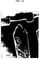
- the undercut regioncan vary in length from the cross-section TEMs of the pad oxide undercut, thus, the undercut region has been observed to vary as much as 70 nm.
- the node dielectricis deposited and "plugs" up the undercut region entirely.
- FIG 14is a cross-section TEM micrograph which shows a 70nm undercut region that is, for the most part, filled entirely with the node dielectric. The presence of this node dielectric protects the pad oxide from being fully undercut and allows for further oxide etches, namely the mask TEOS etch and the collar oxide etch to define the bottom of the buried strap.
- the primary benefits of the method of the present inventionare lower cost and reduced process time. In particular a cost savings of approximately 11% and a process time savings achieved through an approximately 49% reduction in the number of processing steps, are realized over the present DT processing methods.
- the method of the present inventiondoes not require any unique tools or tool development.
- the elimination of the first and second polysilicon fillssubstantially avoids the possibility of oxide residuals from either incomplete collar etching, or interfacial oxide buildup of the first As-doped polysilicon fill (e.g. formed during the waiting period between the first and second polysilicon fills).
- the corresponding reduction from three DT poly CMPs to one DT poly CMPsubstantial overcomes or reduces the problem of pad SiN erosion due to the multiple CMPs.
- the presence of a thermally-grown oxide for the collar oxideavoids the diffusion of oxygen into the collar oxide and generally reduces the formation of the vertical bird's beak of the collar oxide. This, in turn, should reduce the tendency of trench-induced dislocations from forming in the array. Still further DT-substrate shorts are generally eliminated since the present invention produces a smooth transition from the thermally grown collar oxide to the node dielectric. Finally, the metals that are typically present in reactive ion etching (RIE) during polyfill recess processes which could adversely affect the storage capacity of the DT are substantially eliminated.
- RIEreactive ion etching
Landscapes
- Engineering & Computer Science (AREA)
- Manufacturing & Machinery (AREA)
- Physics & Mathematics (AREA)
- Condensed Matter Physics & Semiconductors (AREA)
- General Physics & Mathematics (AREA)
- Computer Hardware Design (AREA)
- Microelectronics & Electronic Packaging (AREA)
- Power Engineering (AREA)
- Semiconductor Memories (AREA)
- Semiconductor Integrated Circuits (AREA)
Abstract
Description
- The present invention relates generally to dynamic random access memories (DRAMs), and more particularly to a method for forming a storage node which utilizes a reduced number of polyfills and chemical-mechanical polishes that provides a smooth transition between the node dielectric and the collar oxide of the storage node.
- Deep trench-based storage devices are commonly used in DRAM cells. Such devices are typically etched 4-8 um deep into the silicon substrate. The process used for forming the deep trench differs between 4 Mb, 16 Mb, 64 Mb, 256 Mb, and 1 GB DRAM cells, however, there are a given number of process steps that are common to each generation of DRAM cell. The commonly performed deep trench processing steps, which constitute a large portion of the cost of making each of these trench-based DRAM cells, are as follows: the deposition of a node dielectric by low pressure chemical vapor deposition (LPCVD) of SiN, the reoxidation of the node dielectric, the deposition of a first polysilicon fill using LPCVD, the chemical mechanical polish of the first polysilicon fill, the etching of a first recess in the first polysilicon fill using reactive ion etching (RIE), the deposition of a collar oxide, the etching of the collar oxide using RIE, the deposition of a second polysilicon fill using LPCVD, and the chemical mechanical polish the second polysilicon fill.
- In the 256 Mb DRAM deep trench process, the connection between the storage trench and its associated array transistor is provided by a third polysilicon fill that is etched 50 nm below the silicon surface. This processing step is commonly referred to as the "buried strap formation". The buried strap process complicates the deep trench process and makes the deep trench process significantly more costly.
- Another problem associated with the 256 Mb DRAM cell process relates to the vulnerability of the top portion of the SiN node dielectric. In current deep trench processing, the node dielectric is etched off the sidewalls of the trench. The depth of the node dielectric etch is determined by the first deep trench recess formed in the first polysilicon fill. The top portion of the node dielectric is susceptible to damage by the deep trench recess, the node dielectric etch, and collar oxide etch processes. The node dielectric thickness presently used is 6nm, however, the final targeted thickness is even thinner or approximately 5 nm. In large deep trench test macros (224 Mb deep trenches), it has been found that shorting between the deep trenches is more prevalent when the first deep trench recess and, the node and collar oxide etch process are used. Conversely, when these processes are not used, the frequency of shorting between the deep trenches is negligible.
- The shorting that occurs between the trenches originates at exposed areas of the deep trench sidewall which are at the top of the node dielectric. An exposed portion of the deep trench sidewall will eventually leave the substrate in contact with the polysilicon fill thus, causing shorts. As the node dielectric is further scaled down to 5 nm, these "extrinsic" fails will become even more ubiquitous.
- It is, therefore, an object of the present invention to provide a simplified method for forming a storage node in a deep trench process which reduces the number of polysilicon fills and chemical-mechanical polishes and also provides a smooth transition between the node dielectric and the collar oxide.
- The present invention is a simplified method of fabricating a storage node for a deep trench-based DRAM on a semiconductor substrate. The method comprises the etching a trench in a surface of the substrate and then forming a layer of dielectric material on a sidewall of the trench. Next, a layer of oxide is grown on the sidewall. A portion of the layer of oxide is then removed from the sidewall in order to orient the layer of oxide a predetermined distance from the surface of the substrate. Finally, the trench is filled with a semiconductive material.
- For a detailed understanding of the present invention, reference should be made to the following detailed description taken in conjunction with the accompanying drawings wherein:
- FIG. 1 is a cross-sectional view through a deep trench DRAM after the deposition of a SiN node dielectric;
- FIG. 2 is a cross-sectional view through the deep trench DRAM of FIG. 1 after filling the trench with resist;
- FIG. 3 is a cross-sectional view through the deep trench DRAM of FIG. 2 after recess etching the resist;
- FIG. 4 is a cross-sectional view through the deep trench DRAM of FIG. 3 after stripping the TEOS mask and a resist clean of the deep trench;
- FIG. 5 is a cross-sectional view through the deep trench DRAM of FIG. 4 after a collar/node reoxidation;
- FIG. 6 is a cross-sectional view through the deep trench DRAM of FIG. 5 after filling the trench with resist;
- FIG. 7 is a cross-sectional view through the deep trench DRAM of FIG. 6 after a collar oxide etch;
- FIG. 8 is a cross-sectional view through the deep trench DRAM of FIG. 7 after filling the trench with polysilicon;
- FIG. 9 is a cross-sectional view through the deep trench DRAM of FIG. 8 after planarization;
- FIGS. 10 and 11 are SEM micrographs after etching the resist down to a previously defined buried plate;
- FIGS. 12 and 13 are SEM micrographs of deep trenches that have been processed according to the present invention; and
- FIG. 14 is a cross-sectional TEM micrograph showing an undercut region associated with the pad oxide of a deep trench DRAM made in accordance with the present invention.
- The present invention describes a method which simplifies the storage node formation portion of the deep trench process by reducing the number of polysilicon fills and chemical-mechanical polishes from three to one and which also provides a smooth transition between the node dielectric and the collar oxide. This is accomplished in the present method by employing a resist fill and a chemical down-steam etching (CDE) technique to etch the node dielectric off the top portion of each of the deep trenches, and a self-defined, thermally-grown collar oxide that is formed during the node reoxidation of the SiN node dielectric.
- Although the method of the present invention will be described in regard to fabricating a 256 Mb DRAM cell, it should be understood that the present method is equally useful for fabricating other generation DRAM cells such as 4, 16 and 64 Mb DRAMs.
- Referring to FIG. 1, a cross-sectional view through one of the
deep trenches 18 etched in asilicon substrate 10 is shown. The method of the present invention is implemented after a first resist fill for buried plate formation (not shown) and node dielectric 20 of SiN has been deposited in thedeep trench 18 using conventional LPCVD techniques. Thedeep trench 18 is formed using conventional RIE techniques. Further, apad oxide layer 12, aSiN pad layer 14, and a deeptrench mask layer 16 of TEOS have been deposited on the surface of thesubstrate 10. - After the node dielectric 20 has been deposited, a second resist fill 22 of for example, AZ 7500, is deposited (without baking) in the
deep trench 18 as shown in FIG. 2. Next, in FIG. 3, a second CDE is used to etch the resist fill 22 to a depth D1 of approximately 1.5 um, this being the depth of a previously defined arsenosilicate glass (ASG)/buried plate (not shown). As can be seen, the node dielectric 20 has been removed entirely from the upper portion of thedeep trench sidewall 19. During the CDE process, additional silicon on the order of approximately 10 nm can be removed from the upper portion of thedeep trench sidewall 19 in order enlarge thedeep trench 18 to account for the later growing of an oxide at the upper portion of thedeep trench sidewall 19 which could hinder the proper filling of thedeep trench 18 with polysilicon. - In FIG. 4, the entire deep
trench mask layer 16 of TEOS that was used for forming thedeep trench 18 has been stripped away using a 7:1 BHF etch for 520s. As shown, the etching is performed without undercutting thepad films - After striping the deep
trench mask layer 16 and performing a resist clean of thedeep trench 18 to remove the resist fill 22, a node reoxidation process is performed. As shown in FIG. 5, the node reoxidation process oxidizes the node dielectric 20 remaining in thedeep trench 18 and grows acollar oxide 24. The node reoxidation process uses a thermal wet oxidation performed at approximately 900°C at 10 m wet O2, to grow thecollar oxide 24 along thedeep trench sidewall 19 to a thickness of approximately 50 nm. - In FIG. 6, the
deep trench 18 has been filled once again with a third resist fill 26 and subsequently recessed using a CDE process down to a depth D2 of between 100 and 150 nm below thesurface 11 of thesilicon substrate 10. - In FIG. 7, a short duration wet etch using a 40:1 BHF (approximately 3 - 4 minutes) or alternatively a 7:1 BHF (approximately 30 - 40 seconds), has been used to remove the
collar oxide 24 off thedeep trench sidewall 19. The wet etch is used to form the lower portion of a buriedstrap 28. After wet etching the resist fill 26 is cleaned from thedeep trench 18. - In FIG. 8, the
deep trench 18 has been filled with an arsenic-dopedpolysilicon 30 which covers the pad SiN 14. Thepolysilicon fill 30 is subsequently planarized down to thepad SiN 14 using a chemical-mechanical polish as shown in FIG. 9. The polysilicon fill and planarization steps described above are performed only once in the method of the present invention as compared to the 3 polysilicon fills and chemical-mechanical polishes of prior art techniques. After the planarization of thepolysilicon fill 30, a buried strap recess process is performed along with the remaining process steps for a 256 Mb DRAM. - The resulting structure created by the method of the present invention can be seen in the SEM micrographs of FIGS. 10 and 11 which show a 256Mb DRAM made in accordance with the present invention after a second CDE recess (i.e. an etch of the resist down to the buried plate depth). As can be seen, there is excellent uniformity between the center and edge chips. FIGS. 12 and 13 are SEM micrographs of deep trenches that have proceeded through the following processing steps: 1) CDE to form the second recess, 2) 7:1 - 520 s BHF etch (mask TEOS strip), 3) resist clean, 4) node reoxidation (900°C - 10 m wet), and 5) intrinsic polyfill. The micrographs of FIGS. 12 and 13 show an oxide, approximately 50 nm thick, along the deep trench sidewall. In addition, at the bottom of the collar oxide, there is a small "bird-beak" shaped structure present at the node/collar intersection. The "bird-beak" shaped structure is important as it provides a smooth transition between the reoxidized node dielectric and the collar oxide. Thus, the probability of deep trench-substrate shorts are greatly reduced. Note that the voids which can be observed in the polysilicon fill underneath the collar oxide (∼ 60 nm in diameter), can be minimized by slightly recessing the deep trench sidewalls as described earlier, by using the CDE after the resist/node dielectric etch, to etch off the top portion of the deep trench.
- A TEOS mask strip of approximately 9 minutes long can be implemented after performing the second CDE due to the presence of the SiN node dielectric present within the undercut region of the pad oxide. This undercut region is formed during the removal of the ASG which forms the buried plate. The undercut region can vary in length from the cross-section TEMs of the pad oxide undercut, thus, the undercut region has been observed to vary as much as 70 nm. However, immediately after the ASG strip, the node dielectric is deposited and "plugs" up the undercut region entirely. FIG 14 is a cross-section TEM micrograph which shows a 70nm undercut region that is, for the most part, filled entirely with the node dielectric. The presence of this node dielectric protects the pad oxide from being fully undercut and allows for further oxide etches, namely the mask TEOS etch and the collar oxide etch to define the bottom of the buried strap.
- The primary benefits of the method of the present invention are lower cost and reduced process time. In particular a cost savings of approximately 11% and a process time savings achieved through an approximately 49% reduction in the number of processing steps, are realized over the present DT processing methods.
- Apart from the cost savings, the method of the present invention does not require any unique tools or tool development. Moreover, in addition to the benefits stemming from the reduction of DT polyfills from three to one as previously described, the elimination of the first and second polysilicon fills substantially avoids the possibility of oxide residuals from either incomplete collar etching, or interfacial oxide buildup of the first As-doped polysilicon fill (e.g. formed during the waiting period between the first and second polysilicon fills). The corresponding reduction from three DT poly CMPs to one DT poly CMP substantial overcomes or reduces the problem of pad SiN erosion due to the multiple CMPs. Further, the presence of a thermally-grown oxide for the collar oxide avoids the diffusion of oxygen into the collar oxide and generally reduces the formation of the vertical bird's beak of the collar oxide. This, in turn, should reduce the tendency of trench-induced dislocations from forming in the array. Still further DT-substrate shorts are generally eliminated since the present invention produces a smooth transition from the thermally grown collar oxide to the node dielectric. Finally, the metals that are typically present in reactive ion etching (RIE) during polyfill recess processes which could adversely affect the storage capacity of the DT are substantially eliminated.
- It should be understood that the embodiments described herein are merely exemplary and that a person skilled in the art may make many variations and modifications to these embodiments utilizing functionally equivalent elements to those described herein. Any and all such variations or modifications as well as others which may become apparent to those skilled in the art, are intended to be included within the scope of the invention as defined by the appended claims.
Claims (20)
- A method of fabricating a storage node for a deep trench-based DRAM on a semiconductor substrate, comprising the steps of:etching a trench in a surface of said substrate;forming a layer of dielectric material on a sidewall of said trench;partially removing said layer of dielectric material in order to expose an underlying region of an upper portion of said sidewall;growing a layer of oxide on said upper portion of said sidewall;removing a portion of said layer of oxide from said sidewall in order to orient said layer of oxide a predetermined distance from said surface of said substrate; andfilling said trench with a semiconductive material.
- The method according to claim 1, wherein said step of forming a layer of dielectric material includes low pressure chemical vapor deposition.
- The method according to claim 2, wherein said layer of dielectric material comprises silicon nitride.
- The method according to claim 1, wherein said step of partially removing said layer of dielectric material includes the steps of:filling said trench with a resist material; andetching said resist a predetermined depth thereby partially removing said layer of dielectric material and exposing said underlying region of said upper portion of said sidewall.
- The method according to claim 1, wherein said step of growing a layer of oxide includes the step of oxidizing both said layer of dielectric material remaining on said sidewall and said exposed region of said sidewall.
- The method according to claim 5, wherein said layer of oxide includes a collar-shaped oxide layer formed on said exposed region of said sidewall.
- The method according to claim 6, wherein said collar-shaped oxide layer is approximately 50 nm in thickness.
- The method according to claim 1, wherein said step of removing a portion of said layer of oxide includes the steps of:filling said trench with a resist material; andetching said resist a predetermined depth thereby removing said portion of said layer of oxide from said sidewall
- The method according to claim 8, wherein said step of etching said resist etches said underlying region of said sidewall exposed by said partial removal said layer of dielectric material.
- The method according to claim 1, further comprising the step of planarizing said substrate after said step of filling.
- The method according to claim 1, wherein said substrate is silicon.
- The method according to claim 1, wherein said semiconductive material is polysilicon.
- The method according to claim 12, wherein said polysilicon is doped with arsenic.
- A method of fabricating a storage node for a deep trench-based DRAM on a silicon substrate, comprising the steps of:etching a trench in a surface of said substrate;depositing a node dielectric on a sidewall of said trench;growing an oxide collar on said sidewall;filling said trench with a resist material;etching said resist a predetermined depth thereby removing a portion of said oxide collar from said sidewall in order to space said oxide collar a predetermined distance from said surface of said substrate; andfilling said trench with polysilicon.
- The method according to claim 14, further including the step of:partially removing said node dielectric prior to said step of growing, in order to expose an underlying region of an upper portion of said sidewall where said oxide collar will be grown, and wherein said step of growing includes:oxidizing both said node dielectric remaining on said sidewall and said exposed region of said sidewall to form said oxide collar.
- The method according to claim 15, wherein said step of partially removing said node dielectric includes the steps of:filling said trench with a resist material; andetching said resist a predetermined depth thereby partially removing said node dielectric and exposing said underlying region of said upper portion of said sidewall.
- The method according to claim 16, wherein said step of etching said resist etches said underlying region of said sidewall exposed by said partial removal said node dielectric.
- The method according to claim 17, wherein said step of etching said resist includes chemical downstream etching.
- The method according to claim 14, further comprising the step of planarizing said substrate after said step of filling.
- The method according to claim 14, wherein said deep trench-based DRAM comprises a 256 Mb DRAM.
Applications Claiming Priority (2)
| Application Number | Priority Date | Filing Date | Title |
|---|---|---|---|
| US610912 | 1990-11-09 | ||
| US08/610,912US5656535A (en) | 1996-03-04 | 1996-03-04 | Storage node process for deep trench-based DRAM |
Publications (2)
| Publication Number | Publication Date |
|---|---|
| EP0794567A2true EP0794567A2 (en) | 1997-09-10 |
| EP0794567A3 EP0794567A3 (en) | 2000-01-12 |
Family
ID=24446904
Family Applications (1)
| Application Number | Title | Priority Date | Filing Date |
|---|---|---|---|
| EP97102901AWithdrawnEP0794567A3 (en) | 1996-03-04 | 1997-02-21 | Process for forming a deep trench-type storage node for a DRAM |
Country Status (5)
| Country | Link |
|---|---|
| US (3) | US5656535A (en) |
| EP (1) | EP0794567A3 (en) |
| JP (1) | JPH09246498A (en) |
| KR (1) | KR970067886A (en) |
| TW (1) | TW375793B (en) |
Cited By (4)
| Publication number | Priority date | Publication date | Assignee | Title |
|---|---|---|---|---|
| DE19852763A1 (en)* | 1998-09-04 | 2000-05-25 | Mosel Vitelic Inc | Trench capacitor, for a DRAM cell, is produced by forming a sacrificial material plug within the trench prior to height reduction etching of an annular dielectric layer on the trench upper side wall region |
| US9443730B2 (en) | 2014-07-18 | 2016-09-13 | Asm Ip Holding B.V. | Process for forming silicon-filled openings with a reduced occurrence of voids |
| US9837271B2 (en) | 2014-07-18 | 2017-12-05 | Asm Ip Holding B.V. | Process for forming silicon-filled openings with a reduced occurrence of voids |
| US10460932B2 (en) | 2017-03-31 | 2019-10-29 | Asm Ip Holding B.V. | Semiconductor device with amorphous silicon filled gaps and methods for forming |
Families Citing this family (56)
| Publication number | Priority date | Publication date | Assignee | Title |
|---|---|---|---|---|
| US5656535A (en)* | 1996-03-04 | 1997-08-12 | Siemens Aktiengesellschaft | Storage node process for deep trench-based DRAM |
| US6013937A (en)* | 1997-09-26 | 2000-01-11 | Siemens Aktiengesellshaft | Buffer layer for improving control of layer thickness |
| US6057216A (en)* | 1997-12-09 | 2000-05-02 | International Business Machines Corporation | Low temperature diffusion process for dopant concentration enhancement |
| US6124206A (en)* | 1997-12-29 | 2000-09-26 | Siemens Aktiengesellschaft | Reduced pad erosion |
| US6190955B1 (en) | 1998-01-27 | 2001-02-20 | International Business Machines Corporation | Fabrication of trench capacitors using disposable hard mask |
| US6066566A (en)* | 1998-01-28 | 2000-05-23 | International Business Machines Corporation | High selectivity collar oxide etch processes |
| US6107135A (en)* | 1998-02-11 | 2000-08-22 | Kabushiki Kaisha Toshiba | Method of making a semiconductor memory device having a buried plate electrode |
| US6310375B1 (en) | 1998-04-06 | 2001-10-30 | Siemens Aktiengesellschaft | Trench capacitor with isolation collar and corresponding manufacturing method |
| US6008104A (en)* | 1998-04-06 | 1999-12-28 | Siemens Aktiengesellschaft | Method of fabricating a trench capacitor with a deposited isolation collar |
| TW471164B (en)* | 1998-06-02 | 2002-01-01 | Ibm | Deep trench-based storage capacitor and method of fabricating |
| WO1999067817A1 (en) | 1998-06-22 | 1999-12-29 | Applied Materials, Inc. | Silicon trench etching using silicon-containing precursors to reduce or avoid mask erosion |
| US6074954A (en)* | 1998-08-31 | 2000-06-13 | Applied Materials, Inc | Process for control of the shape of the etch front in the etching of polysilicon |
| US6194736B1 (en) | 1998-12-17 | 2001-02-27 | International Business Machines Corporation | Quantum conductive recrystallization barrier layers |
| TW415010B (en)* | 1999-04-20 | 2000-12-11 | Mosel Vitelic Inc | Method for fabricating trench capacitor |
| US6236077B1 (en) | 1999-04-20 | 2001-05-22 | International Business Machines Corporation | Trench electrode with intermediate conductive barrier layer |
| US6259129B1 (en) | 1999-04-20 | 2001-07-10 | International Business Machines Corporation | Strap with intrinsically conductive barrier |
| US6387810B2 (en)* | 1999-06-28 | 2002-05-14 | International Business Machines Corporation | Method for homogenizing device parameters through photoresist planarization |
| US6271142B1 (en) | 1999-07-29 | 2001-08-07 | International Business Machines Corporation | Process for manufacture of trench DRAM capacitor buried plates |
| EP1077475A3 (en)* | 1999-08-11 | 2003-04-02 | Applied Materials, Inc. | Method of micromachining a multi-part cavity |
| US6214686B1 (en) | 1999-09-01 | 2001-04-10 | International Business Machines Corporation | Spatially offset deep trenches for high density DRAMS |
| DE19956078B4 (en)* | 1999-11-22 | 2006-12-28 | Infineon Technologies Ag | Method for producing an insulation collar in a trench capacitor |
| US6833079B1 (en) | 2000-02-17 | 2004-12-21 | Applied Materials Inc. | Method of etching a shaped cavity |
| US6415431B1 (en) | 2000-02-18 | 2002-07-02 | International Business Machines Corporation | Repair of phase shift materials to enhance adhesion |
| US6429092B1 (en)* | 2000-06-19 | 2002-08-06 | Infineon Technologies Ag | Collar formation by selective oxide deposition |
| US6417063B1 (en) | 2000-06-22 | 2002-07-09 | Infineon Technologies Richmond, Lp | Folded deep trench capacitor and method |
| US6573137B1 (en)* | 2000-06-23 | 2003-06-03 | International Business Machines Corporation | Single sided buried strap |
| DE10056256B4 (en)* | 2000-11-14 | 2004-11-25 | Promos Technologies, Inc. | New technique to improve the capacity of a deep trench by increasing its surface area |
| US6451702B1 (en)* | 2001-02-16 | 2002-09-17 | International Business Machines Corporation | Methods for forming lateral trench optical detectors |
| US6518118B2 (en) | 2001-03-15 | 2003-02-11 | International Business Machines Corporation | Structure and process for buried bitline and single sided buried conductor formation |
| EP1404481B1 (en)* | 2001-03-22 | 2006-04-19 | Xsil Technology Limited | A laser machining system and method |
| US6670235B1 (en) | 2001-08-28 | 2003-12-30 | Infineon Technologies Ag | Process flow for two-step collar in DRAM preparation |
| DE10162908B4 (en)* | 2001-12-20 | 2006-09-07 | Promos Technologies, Inc. | A method of fabricating a capacitor dielectric structure and capacitor dielectric structure |
| US6867089B2 (en)* | 2002-01-28 | 2005-03-15 | Nanya Technology Corporation | Method of forming a bottle-shaped trench in a semiconductor substrate |
| TWI291735B (en)* | 2002-01-28 | 2007-12-21 | Nanya Technology Corp | Method for forming bottle-shaped trench in semiconductor substrate |
| US6797636B2 (en)* | 2002-05-31 | 2004-09-28 | Infineon Technologies Ag | Process of fabricating DRAM cells with collar isolation layers |
| US6635526B1 (en) | 2002-06-07 | 2003-10-21 | Infineon Technologies Ag | Structure and method for dual work function logic devices in vertical DRAM process |
| US6905944B2 (en)* | 2003-05-08 | 2005-06-14 | International Business Machines Corporation | Sacrificial collar method for improved deep trench processing |
| US6838334B1 (en) | 2003-07-30 | 2005-01-04 | International Business Machines Corporation | Method of fabricating a buried collar |
| KR100529632B1 (en)* | 2003-10-01 | 2005-11-17 | 동부아남반도체 주식회사 | Semiconductor device and fabrication method thereof |
| US6974991B2 (en)* | 2003-10-29 | 2005-12-13 | International Business Machines Corp. | DRAM cell with buried collar and self-aligned buried strap |
| US7276751B2 (en)* | 2005-09-09 | 2007-10-02 | International Business Machines Corporation | Trench metal-insulator-metal (MIM) capacitors integrated with middle-of-line metal contacts, and method of fabricating same |
| KR100707803B1 (en)* | 2005-10-28 | 2007-04-17 | 주식회사 하이닉스반도체 | Method for manufacturing a semiconductor device having a recess gate |
| US7410862B2 (en)* | 2006-04-28 | 2008-08-12 | International Business Machines Corporation | Trench capacitor and method for fabricating the same |
| US7375413B2 (en)* | 2006-05-26 | 2008-05-20 | International Business Machines Corporation | Trench widening without merging |
| WO2008094529A1 (en)* | 2007-01-29 | 2008-08-07 | Jeffrey Jacob Cernohous | Compositions and methods for producing high strength composites |
| US7846791B2 (en)* | 2007-11-08 | 2010-12-07 | International Business Machines Corporation | Structure for a trench capacitor |
| US20100240190A1 (en)* | 2009-03-19 | 2010-09-23 | United Microelectronics Corp. | Method for fabricating deep trench capacitor |
| US8021945B2 (en)* | 2009-04-14 | 2011-09-20 | International Business Machines Corporation | Bottle-shaped trench capacitor with enhanced capacitance |
| US8227311B2 (en) | 2010-10-07 | 2012-07-24 | International Business Machines Corporation | Method of forming enhanced capacitance trench capacitor |
| US9837254B2 (en) | 2014-08-12 | 2017-12-05 | Lam Research Corporation | Differentially pumped reactive gas injector |
| US10825652B2 (en) | 2014-08-29 | 2020-11-03 | Lam Research Corporation | Ion beam etch without need for wafer tilt or rotation |
| US9406535B2 (en) | 2014-08-29 | 2016-08-02 | Lam Research Corporation | Ion injector and lens system for ion beam milling |
| US9536748B2 (en) | 2014-10-21 | 2017-01-03 | Lam Research Corporation | Use of ion beam etching to generate gate-all-around structure |
| US9779955B2 (en) | 2016-02-25 | 2017-10-03 | Lam Research Corporation | Ion beam etching utilizing cryogenic wafer temperatures |
| KR20250011246A (en) | 2019-02-28 | 2025-01-21 | 램 리써치 코포레이션 | Ion beam etching with sidewall cleaning |
| US12334345B2 (en)* | 2021-05-27 | 2025-06-17 | Fujian Jinhua Integrated Circuit Co., Ltd. | Dynamic random access memory device with active regions of different profile roughness and method for forming the same |
Family Cites Families (29)
| Publication number | Priority date | Publication date | Assignee | Title |
|---|---|---|---|---|
| US3943047A (en)* | 1974-05-10 | 1976-03-09 | Bell Telephone Laboratories, Incorporated | Selective removal of material by sputter etching |
| US4016062A (en)* | 1975-09-11 | 1977-04-05 | International Business Machines Corporation | Method of forming a serrated surface topography |
| US4128765A (en)* | 1976-10-29 | 1978-12-05 | Joseph Franks | Ion beam machining techniques and apparatus |
| CA1053627A (en)* | 1976-12-09 | 1979-05-01 | Lowell A. Wilson | Automatic wicketted bag loader |
| US4214966A (en)* | 1979-03-20 | 1980-07-29 | Bell Telephone Laboratories, Incorporated | Process useful in the fabrication of articles with metallized surfaces |
| US4309267A (en)* | 1980-07-21 | 1982-01-05 | Bell Telephone Laboratories, Incorporated | Reactive sputter etching apparatus |
| US4502913A (en)* | 1982-06-30 | 1985-03-05 | International Business Machines Corporation | Total dielectric isolation for integrated circuits |
| JPS59208749A (en)* | 1983-05-12 | 1984-11-27 | Nec Corp | Manufacture of semiconductor device |
| US5225697A (en)* | 1984-09-27 | 1993-07-06 | Texas Instruments, Incorporated | dRAM cell and method |
| JPS62125680A (en)* | 1985-11-26 | 1987-06-06 | Nec Corp | Manufacture of semiconductor device |
| US4801988A (en)* | 1986-10-31 | 1989-01-31 | International Business Machines Corporation | Semiconductor trench capacitor cell with merged isolation and node trench construction |
| EP0283964B1 (en)* | 1987-03-20 | 1994-09-28 | Nec Corporation | Dynamic random access memory device having a plurality of improved one-transistor type memory cells |
| JPH01149572A (en)* | 1987-12-05 | 1989-06-12 | Toshiba Corp | Image reader |
| JPH01149957A (en)* | 1987-12-07 | 1989-06-13 | Hitachi Ltd | Thin film forming apparatus and thin film forming method |
| US5205902A (en)* | 1989-08-18 | 1993-04-27 | Galileo Electro-Optics Corporation | Method of manufacturing microchannel electron multipliers |
| JP2932650B2 (en)* | 1990-09-17 | 1999-08-09 | 松下電器産業株式会社 | Manufacturing method of microstructure |
| US5096849A (en)* | 1991-04-29 | 1992-03-17 | International Business Machines Corporation | Process for positioning a mask within a concave semiconductor structure |
| JPH06163851A (en)* | 1991-06-07 | 1994-06-10 | Texas Instr Japan Ltd | Semiconductor device and manufacturing method thereof |
| US5422294A (en)* | 1993-05-03 | 1995-06-06 | Noble, Jr.; Wendell P. | Method of making a trench capacitor field shield with sidewall contact |
| JP3480745B2 (en)* | 1993-09-16 | 2003-12-22 | 株式会社東芝 | Method for manufacturing semiconductor device |
| US5360758A (en)* | 1993-12-03 | 1994-11-01 | International Business Machines Corporation | Self-aligned buried strap for trench type DRAM cells |
| US5395786A (en)* | 1994-06-30 | 1995-03-07 | International Business Machines Corporation | Method of making a DRAM cell with trench capacitor |
| US5658816A (en)* | 1995-02-27 | 1997-08-19 | International Business Machines Corporation | Method of making DRAM cell with trench under device for 256 Mb DRAM and beyond |
| US5525531A (en)* | 1995-06-05 | 1996-06-11 | International Business Machines Corporation | SOI DRAM with field-shield isolation |
| US5692281A (en)* | 1995-10-19 | 1997-12-02 | International Business Machines Corporation | Method for making a dual trench capacitor structure |
| US5827765A (en)* | 1996-02-22 | 1998-10-27 | Siemens Aktiengesellschaft | Buried-strap formation in a dram trench capacitor |
| US5656535A (en)* | 1996-03-04 | 1997-08-12 | Siemens Aktiengesellschaft | Storage node process for deep trench-based DRAM |
| US5717628A (en)* | 1996-03-04 | 1998-02-10 | Siemens Aktiengesellschaft | Nitride cap formation in a DRAM trench capacitor |
| US5937296A (en)* | 1996-12-20 | 1999-08-10 | Siemens Aktiengesellschaft | Memory cell that includes a vertical transistor and a trench capacitor |
- 1996
- 1996-03-04USUS08/610,912patent/US5656535A/ennot_activeExpired - Fee Related
- 1997
- 1997-01-21USUS08/784,558patent/US5849638A/ennot_activeExpired - Fee Related
- 1997-02-21EPEP97102901Apatent/EP0794567A3/ennot_activeWithdrawn
- 1997-02-27TWTW086102394Apatent/TW375793B/ennot_activeIP Right Cessation
- 1997-03-03KRKR1019970006875Apatent/KR970067886A/ennot_activeWithdrawn
- 1997-03-04JPJP9063929Apatent/JPH09246498A/enactivePending
- 1998
- 1998-07-01USUS09/108,619patent/US6153474A/ennot_activeExpired - Lifetime
Cited By (5)
| Publication number | Priority date | Publication date | Assignee | Title |
|---|---|---|---|---|
| DE19852763A1 (en)* | 1998-09-04 | 2000-05-25 | Mosel Vitelic Inc | Trench capacitor, for a DRAM cell, is produced by forming a sacrificial material plug within the trench prior to height reduction etching of an annular dielectric layer on the trench upper side wall region |
| DE19852763B4 (en)* | 1998-09-04 | 2004-04-29 | Mosel Vitelic Inc. | Method of making a trench capacitor |
| US9443730B2 (en) | 2014-07-18 | 2016-09-13 | Asm Ip Holding B.V. | Process for forming silicon-filled openings with a reduced occurrence of voids |
| US9837271B2 (en) | 2014-07-18 | 2017-12-05 | Asm Ip Holding B.V. | Process for forming silicon-filled openings with a reduced occurrence of voids |
| US10460932B2 (en) | 2017-03-31 | 2019-10-29 | Asm Ip Holding B.V. | Semiconductor device with amorphous silicon filled gaps and methods for forming |
Also Published As
| Publication number | Publication date |
|---|---|
| EP0794567A3 (en) | 2000-01-12 |
| TW375793B (en) | 1999-12-01 |
| US5849638A (en) | 1998-12-15 |
| US5656535A (en) | 1997-08-12 |
| KR970067886A (en) | 1997-10-13 |
| US6153474A (en) | 2000-11-28 |
| JPH09246498A (en) | 1997-09-19 |
Similar Documents
| Publication | Publication Date | Title |
|---|---|---|
| US5656535A (en) | Storage node process for deep trench-based DRAM | |
| US5933748A (en) | Shallow trench isolation process | |
| KR100343353B1 (en) | Low-resistance salicide fill for trench capacitors | |
| US6177698B1 (en) | Formation of controlled trench top isolation layers for vertical transistors | |
| EP0656655B1 (en) | A self-aligned buried strap for trench type DRAM cells | |
| US6359299B1 (en) | Apparatus and method for forming controlled deep trench top isolation layers | |
| EP1198832B1 (en) | Method of making a buried strap for a trench capacitor | |
| US6703273B2 (en) | Aggressive capacitor array cell layout for narrow diameter DRAM trench capacitor structures via SOI technology | |
| US6069058A (en) | Shallow trench isolation for semiconductor devices | |
| US6967136B2 (en) | Method and structure for improved trench processing | |
| JPS62269335A (en) | Manufacture of semiconductor device | |
| JPH11145275A (en) | Shallow trench isolation structure and method of forming the same | |
| US6509226B1 (en) | Process for protecting array top oxide | |
| US6040213A (en) | Polysilicon mini spacer for trench buried strap formation | |
| US6420750B1 (en) | Structure and method for buried-strap with reduced outdiffusion | |
| US6358785B1 (en) | Method for forming shallow trench isolation structures | |
| US20030124805A1 (en) | High aspect ratio PBL SiN barrier formation | |
| JP2004523918A (en) | Semiconductor memory cell and method of manufacturing the same | |
| US6964898B1 (en) | Method for fabricating deep trench capacitor | |
| US6403492B1 (en) | Method of manufacturing semiconductor devices with trench isolation | |
| KR100204023B1 (en) | Method of forming device isolation film in semiconductor device | |
| EP0949674A2 (en) | Method of forming buried strap for trench capacitor | |
| US6204127B1 (en) | Method of manufacturing bit lines in memory | |
| KR910002012B1 (en) | Method for production of dram | |
| KR20020003018A (en) | Shallow trench isolation method using silicon liner |
Legal Events
| Date | Code | Title | Description |
|---|---|---|---|
| PUAI | Public reference made under article 153(3) epc to a published international application that has entered the european phase | Free format text:ORIGINAL CODE: 0009012 | |
| AK | Designated contracting states | Kind code of ref document:A2 Designated state(s):DE FR GB IT | |
| PUAL | Search report despatched | Free format text:ORIGINAL CODE: 0009013 | |
| AK | Designated contracting states | Kind code of ref document:A3 Designated state(s):DE FR GB IT | |
| RIC1 | Information provided on ipc code assigned before grant | Free format text:7H 01L 21/8242 A, 7H 01L 27/108 B, 7H 01L 21/70 B | |
| 17P | Request for examination filed | Effective date:20000619 | |
| RAP1 | Party data changed (applicant data changed or rights of an application transferred) | Owner name:INTERNATIONAL BUSINESS MACHINES CORPORATION Owner name:INFINEON TECHNOLOGIES AG | |
| 17Q | First examination report despatched | Effective date:20070323 | |
| STAA | Information on the status of an ep patent application or granted ep patent | Free format text:STATUS: THE APPLICATION IS DEEMED TO BE WITHDRAWN | |
| 18D | Application deemed to be withdrawn | Effective date:20090901 |