EP0788048B1 - Display apparatus interface - Google Patents
Display apparatus interfaceDownload PDFInfo
- Publication number
- EP0788048B1 EP0788048B1EP97300289AEP97300289AEP0788048B1EP 0788048 B1EP0788048 B1EP 0788048B1EP 97300289 AEP97300289 AEP 97300289AEP 97300289 AEP97300289 AEP 97300289AEP 0788048 B1EP0788048 B1EP 0788048B1
- Authority
- EP
- European Patent Office
- Prior art keywords
- pixel
- logic
- clock signal
- video
- word
- Prior art date
- Legal status (The legal status is an assumption and is not a legal conclusion. Google has not performed a legal analysis and makes no representation as to the accuracy of the status listed.)
- Expired - Lifetime
Links
- 230000004044responseEffects0.000claimsdescription5
- 238000004891communicationMethods0.000description9
- 230000005540biological transmissionEffects0.000description7
- 238000010586diagramMethods0.000description5
- 239000003086colorantSubstances0.000description4
- 239000004973liquid crystal related substanceSubstances0.000description4
- 239000002131composite materialSubstances0.000description3
- 239000013307optical fiberSubstances0.000description3
- 238000012545processingMethods0.000description3
- 238000006243chemical reactionMethods0.000description2
- 238000005516engineering processMethods0.000description2
- 238000012546transferMethods0.000description2
- 208000032365Electromagnetic interferenceDiseases0.000description1
- 230000002411adverseEffects0.000description1
- 230000015556catabolic processEffects0.000description1
- 238000004590computer programMethods0.000description1
- 238000012937correctionMethods0.000description1
- 238000013500data storageMethods0.000description1
- 238000006731degradation reactionMethods0.000description1
- 230000001419dependent effectEffects0.000description1
- 238000001514detection methodMethods0.000description1
- 239000000835fiberSubstances0.000description1
- 230000006870functionEffects0.000description1
- 238000007726management methodMethods0.000description1
- 238000000034methodMethods0.000description1
- 238000012986modificationMethods0.000description1
- 230000004048modificationEffects0.000description1
- 239000005304optical glassSubstances0.000description1
- 239000013308plastic optical fiberSubstances0.000description1
- 238000011084recoveryMethods0.000description1
- 230000000717retained effectEffects0.000description1
- 238000000926separation methodMethods0.000description1
- 230000001360synchronised effectEffects0.000description1
- 230000000007visual effectEffects0.000description1
Images


Classifications
- G—PHYSICS
- G09—EDUCATION; CRYPTOGRAPHY; DISPLAY; ADVERTISING; SEALS
- G09G—ARRANGEMENTS OR CIRCUITS FOR CONTROL OF INDICATING DEVICES USING STATIC MEANS TO PRESENT VARIABLE INFORMATION
- G09G5/00—Control arrangements or circuits for visual indicators common to cathode-ray tube indicators and other visual indicators
- G09G5/003—Details of a display terminal, the details relating to the control arrangement of the display terminal and to the interfaces thereto
- G09G5/006—Details of the interface to the display terminal
- G—PHYSICS
- G09—EDUCATION; CRYPTOGRAPHY; DISPLAY; ADVERTISING; SEALS
- G09G—ARRANGEMENTS OR CIRCUITS FOR CONTROL OF INDICATING DEVICES USING STATIC MEANS TO PRESENT VARIABLE INFORMATION
- G09G2340/00—Aspects of display data processing
- G09G2340/04—Changes in size, position or resolution of an image
- G—PHYSICS
- G09—EDUCATION; CRYPTOGRAPHY; DISPLAY; ADVERTISING; SEALS
- G09G—ARRANGEMENTS OR CIRCUITS FOR CONTROL OF INDICATING DEVICES USING STATIC MEANS TO PRESENT VARIABLE INFORMATION
- G09G2360/00—Aspects of the architecture of display systems
- G09G2360/02—Graphics controller able to handle multiple formats, e.g. input or output formats
- G—PHYSICS
- G09—EDUCATION; CRYPTOGRAPHY; DISPLAY; ADVERTISING; SEALS
- G09G—ARRANGEMENTS OR CIRCUITS FOR CONTROL OF INDICATING DEVICES USING STATIC MEANS TO PRESENT VARIABLE INFORMATION
- G09G2370/00—Aspects of data communication
- G09G2370/04—Exchange of auxiliary data, i.e. other than image data, between monitor and graphics controller
- G09G2370/042—Exchange of auxiliary data, i.e. other than image data, between monitor and graphics controller for monitor identification
Definitions
- the present inventionrelates to apparatus for generating serial video bit streams, display apparatus for receiving such serial video bit streams, and display systems comprising such apparatus.
- a typical display systemcomprises a display device such as a cathode ray tube (CRT) display and a host computer system connected to the display device.
- the computer systemIn operation, the computer system generates image data for producing a picture on the screen of the display device.
- the computer systeminitially generates the image data in the digital domain.
- a digital to analog convertor in the computer systemthen converts the image data into analog video signals for transfer to the display device.
- Such display systemsprovide acceptable performance provided the display device is responsive to analog video signals.
- some display devicesfor example liquid crystal display screens, require a digital video signal.
- some display devicesinclude digital signal processing systems for processing input video signals in the interests of performance enhancement.
- each pixel of an imageis represented by a fixed number of bits. Therefore each pixel has a correspondingly finite colour depth.
- Current liquid crystal displaysallocate between 4 and 6 bits per colour.
- the colour depthis 8 bits per colour.
- some digital video output devices or "Palettes"can now provide 10 bits per colour.
- the number of bits per colourcan vary in such Palettes from one colour to the next.
- greenis allocated more bits than red and blue, for example.
- EP-A-0,460,961discloses a signal communication system for serially transmitting display data between a CPU and a display device, which is intended to increase the communication rate and to reduce the transmission error rate.
- a display systemcomprising a digital video source coupled to a digital display device via a digital interface having a timing channel for carrying a pixel clock signal from the video source to the display device and a digital video channel for carrying a digital video bit stream from the video source to the display device
- the video sourcecomprises a pixel clock generator for generating the pixel clock signal, palette logic for outputting a pixel data word on each pulse of the pixel clock signal, first shift clock generator logic for multiplying the pixel clock signal by the number of bits in the pixel word to produce a shift clock signal, and serialiser logic for serially outputting the pixel data word in the serial bit stream at the shift clock signal rate
- the display devicecomprises a display screen for producing a pixel of an image at least partially in response to the pixel data word; a timing receiver for receiving a pixel clock signal CLK' from the video source; second shift clock generator logic for multiplying the pixel clock signal by the number of bits in the pixel word, and des
- the interfacecomprises a control channel for communicating the number of bits in the pixel word from the video source to the display device.
- the present inventionextends to a computer system comprising a processor, a memory, and such a display system.
- apparatus for generating a serial video bit streamcomprising: a pixel clock generator for generating a pixel clock signal; palette logic for generating a pixel data word on each pulse of the pixel clock signal; shift clock generator logic for multiplying the pixel clock signal by the number of bits in the pixel data word to produce a shift clock signal; and, serialiser logic for serially outputting the pixel data word in a serial bit stream at the shift clock signal rate.
- control logicis connected to the shift clock generator logic for reading the number of bits in the pixel data word from an external source.
- cross-point switch logicfor transferring the pixel data word generated by the palette logic to the serialiser logic.
- error logicfor generating an error code corresponding to the pixel data word and for adding the error code to the serial bit stream.
- a display apparatuscomprising: a display screen for producing a pixel of an image at least partially in response to a pixel data word; a timing receiver for receiving a pixel clock signal from an external video source; shift clock generator logic for multiplying the pixel clock signal by the number of bits in the pixel word to generate a shift clock signal; and, deserialiser logic for receiving an input video bit stream at the shift clock signal rate to generate the pixel word.
- the display apparatuscomprises control logic connected to the shift clock generator logic for reading the number of bits in the pixel data word from an external source.
- error logicfor detecting an error in the pixel word and from an error code in the serial bit stream.
- the pixel worddefines a pixel of a monochrome video image.
- the pixel worddefines a colour component of a pixel of a colour video image.
- the present inventionadvantageously provides a display interface which is capable of linking a video source such as a computer system unit or work-station to any one of a range of digital display devices irrespective of refresh rate, colour depth, and resolution. Such compatibility is achieved by providing the interface with variable colour depth, a timing channel, and a simple configuration method.
- an example of a display system of the present inventioncomprises a digital display device 10 such as a liquid crystal display, projection display, cathode ray tube display, or the like.
- a computer system unit 20such as a personal computer, work-station. or the like, has an internal video output sub-system connected to display device 10 via an interface 50.
- Input devicesincluding a keyboard 30 and pointing device 40 are connected to data input ports of system unit 20.
- Pointing devicemay be in the form of a mouse, tracker ball, joystick, touch-screen, or the like.
- System unit 20comprises a central processing unit (CPU) such as a microprocessor, memory, and mass data storage means such as a hard disk drive all interconnected by a bus architecture.
- CPUcentral processing unit
- Bus architecturefurther extends to the video sub-system, the data input ports, and additional data output ports for connection to, for example, a printer.
- CPUexecutes computer program code stored in the memory or retrieved from the mass storage means to produce, via the video sub-system, digital video signals for driving display device 10 to generate a visual output.
- a usercan control execution of the program code by the CPU via keyboard 30 and pointing device 40.
- interface 50comprises: Red, Green, and Blue digital video channels R, G , and B; a timing channel TC; and, a control channel I.
- the video sub-system of system unit 20comprises a colour digital output palette 200 having an N bit video data output, a pixel clock output CLK, a data valid output DV, and line and frame sync outputs Hsync and Vsync.
- the N bit video data outputis connected to an N X N cross-point switch 210.
- Sync outputs Hsync and Vsync and pixel clock output CLKprovide inputs to a summing logic block 240.
- the output of summing block 240provides timing channel TC of interface 50.
- the output of cross-point 210is connected to each of three parallel input serial output shift registers 260-262.
- Each of registers 260-262has phase locked loop and counter logic 270-271.
- the data valid output of palette 200is connected to an enable input of each of registers 260-262.
- the serial output of each register 260-262is connected, via a buffer amplifier 250-252, to a different one of video channels R, G, and B of interface 50.
- Each channel R, G, and Bcorresponds to a different one of the three primary colours Red, Green and Blue.
- Control channel I of interface cable 50is connected to a communications logic block 230.
- a control logic block 220is coupled to logic block 230 and palette 200.
- Control logic block 220has three control outputs BPP Cntl each 4 bits wide and each connected to a different one of phase locked loop and counter logic blocks 270-272.
- the pixel clock output CLK from Palette 200is also connected to each of logic blocks 270-272.
- data to be displayed on display device 10is written by the CPU of system unit 20 to a video memory (not shown) of the video sub-system.
- the data stored in the video memoryis converted by palette 200 into a colour data set for each pixel of the image to be displayed on display device 10.
- the pixel data set corresponding to each pixelis presented in parallel at the output of palette 200 as an N bit wide word.
- Data valid signal DVis generated by palette 200 shortly thereafter to indicate that the N bit word has stabilised.
- Each of the primary colours for a pixelis represented by a different sub-set of bits of the corresponding N bit word. Thus all three colours are presented simultaneously.
- the N bit wordmay be 16 bits wide and the Red, Green and Blue colour data may be 5, 6, and 5 bits wide respectively.
- Palette 200also generates a pixel clock signal CLK synchronised to presentation of each N bit word.
- Each N bit wordis routed, via cross point switch 210, to registers 260-262.
- the operation of cross point switch 210will be described in detail shortly.
- the red colour datais routed to register 260; the green colour data is routed to register 261; and the blue colour data is routed to register 262.
- Each colour data subsetis loaded into the corresponding register in parallel in response to data valid signal DV.
- Each register 260-262acts as a serialiser. Specifically, each register sequentially sends bits of colour data along the corresponding video channel to display device 10. The rate of transmission of bits from each register 260-262 to display device 10 is higher than the pixel clock by a factor equal to the number of bits constituting the corresponding colour data.
- the rate of transmission from the shift registeris controlled by a shift register clock.
- the shift register clockis generated by the corresponding phase locked loop and counter logic 270-272.
- the corresponding phase locked loop and counter logicmultiplies pixel clock signal CLK by the number of bits constituting the corresponding colour data to generate the shift register clock.
- Each colour datais thus transmitted at the shift register clock frequency of the corresponding register 260-262.
- error logicfor producing a parity bit, CRC checksum, or other error code for permitting error detection.
- the error codeis sent with the pixel data and decoded in display device 10. It will be appreciated that display device 10 may, in turn comprise error correction logic for correcting received data based on the decoded error code.
- Summing logic 240sums sync signals Hsync and Vsync and pixel clock signal CLK (or at least a sub-multiple thereof) to generate a composite timing signal on timing channel TC of interface 50.
- pixel clock signal CLKis filtered to reduce high frequency content and reduced in amplitude prior to summation to minimise potential for electro-magnetic interference.
- display device 10comprises a communications logic block 100 connected to control channel I of interface 50.
- Communications logic block 100is connected to a display processor 120 of display device 10 and a control logic block 110.
- the red, green and blue video channels R, G, and B of interface 50are each connected, via a buffer amplifier 140-142, to a different one of a group of three serial input parallel output shift registers 150-152.
- Each of registers 150-152comprises phase locked loop and counter logic 160-162.
- Control logic block 110has three control outputs each 4 bits wide and each connected to different one of phase locked loop and control logic 160-162.
- Each register 150-152has a data valid output DV' in addition to a parallel colour data output R', G' and B'.
- Timing channel TC of interface 50is connected to a timing separation logic block 130 having a pixel clock output CLK' and line and frame sync outputs Hsync' and Vsync'.
- Pixel clock output CLK'is connected to the each of logic blocks 160-162.
- buffer amplifiers 140-142receive serial colour data bits for each pixel from the corresponding video channels R, G, and B. The received data bits are delivered by buffer amplifiers 140-142 to the serial inputs of the corresponding registers 150-152.
- Sync separator logic 130separates line and frame sync signals Hsync and Vsync from the composite signal on timing channel TC of interface 50. Separator logic 130 also includes clock recovery logic for recovering pixel clock signal CLK' from the composite timing signal.
- the bits per pixel value for each video channelis recovered by communications logic 100 from control channel I of interface 50. Communication logic 100 supplies the bits per pixel values to control logic 110. Control logic 110 programmes phase locked loop and counter logic 160-162 of registers 150-152 as a function of the received bits per pixel values.
- Each register 150-152sequentially loads bits of colour data from the corresponding video channel R, G, and B.
- the rate of reception of bits by each register 150-152is higher than recovered pixel clock CLK' by a factor equal to the number of bits constituting the corresponding colour data.
- the rate of reception by the register 150-152is controlled by a shift register clock.
- the shift register clockis generated by the corresponding phase locked loop and counter logic 160-162.
- the corresponding phase locked loop and counter logic 160-162multiplies recovered pixel clock signal CLK' by the number of bits constituting the corresponding colour data to generate the shift register clock. Each colour data is thus received at the shift register clock frequency of the corresponding register 150-152.
- each register 150-152is programmed with a corresponding bits per pixel value by control logic block 110.
- the colour data P', G', and B'is presented at the parallel output of the corresponding registers 160-162' simultaneously thereby reconstructing the N bit pixel data word.
- Each register 150-152generates a data valid signal DV' to indicate that the corresponding colour data at the parallel output of the register 150-152 has stabilised. It will be appreciated that each register 150-152 acts as a deserialiser.
- a preferred initialisation sequence for the examples of the present invention hereinbefore describedcommences in system unit 20 by the video sub-system disabling timing channel TC.
- the sequencecommences with display processor 120 resetting the display drive circuitry and then waiting for a command from system unit 10. with the timing channel disabled, the video sub-system then sends a token to the display device 10 via control channel I of interface 50 and waits for display device to return the token, again via control channel I. If, after a predetermined period of time the video sub-system has yet to receive the token from display device 10, the video sub-system send another token. On receipt of the token from the display device 10, the video sub-system sends a RESET instruction to display device 10.
- Display Device 10responds to the RESET instruction by resetting the display drive circuitry and by sending video sub-system performance data, indicative of the operating parameters of display device 10, via control channel I.
- the performance datacomprises pixel addressability (or resolution) ADDR; maximum REFRESH rate; and maximum BPP (bits per pixel) for each video channel R, G, and B.
- Display device 10then waits for the next command from the video sub-system.
- the video sub-systemreads the performance data sent by display device 10. If the addressability value received from display device 10, DISPLAY ADDR is less than the addressability value currently retained by the video sub-system, PC ADDR, then the video sub-system sets PC ADDR to DISPLAY ADDR. Otherwise, the video sub-system sets PC ADDR to maximum.
- the video sub-systemsets PC REFRESH to less than or equal to DISPLAY REFRESH. Furthermore, for each video channel R, G, and B, if the corresponding bits per pixel value received from display device 10, DISPLAY BPP is less than the corresponding bits per pixel value stored by the video sub-system, PC BPP, then the video sub-system sets PC BPP to DISPLAY BPP. Otherwise, the video sub-system sets PC BPP to maximum.
- the video sub-systemthen sends the bits per pixel value, PC BPP, for each video channel R, G, and B, to display device 10 via control channel r.
- display device 10programs the phase locked loop and counter logic 160-162 of each register 150-152 in preparation to receive video data streams from the video sub-system.
- Display processor 120sets a STATUS code to indicate that display device 10 is ready for operation.
- Display device 10then waits for the next command from the video sub-system.
- the video sub-systemturns on timing channel TC and reads the STATUS code from display device 10.
- the above described sequence of eventsis the same in system unit 20 for power on, re-boot, and display resolution mode changes. In display device 10, the above sequence of events is the same for power on and return from a stand-by (eg: power management) state.
- the above initialisation sequenceallows the video sub-system and display device 10 to have different abilities.
- the sequenceselects the highest mode of operation common to both display device 10 and the video sub-system. It will be appreciated that any other common mode may also be selected by appropriate programming of the video sub-system.
- each of channels I, R, G, B and TC of interface 50may be formed from any of twisted pair cable, coaxial cable, plastic optical fibre, or glass optical fibre. However, the former three are generally only suitable for use over relatively short distances (eg: less than 10 m). Beyond such distances, signal degradation tends to adversely affect performance of the display system.
- each of video channels R, G, and Bmay be implemented in interface 50 by a separate path (eg: wire or fibre).
- a single pathmay be employed by all of video channels R, G and B with each channel occupying a different portion of the bandwidth of the transmission media and transducers forming the path.
- the speed of transfer of video data via interface 50may be 15 times greater than the pixel clock speed.
- the transmission media employed in video channels R, G, and Bmay differ from that employed in timing channel TC.
- video channels R, G and Bmay be implemented by optical fibre and timing channel TC may be implemented by coax.
- a problem with such arrangementsis that the different transmission media have different propagation velocities. The difference in propagation velocity leads to a phase error at display device 10. There is maximum permissible phase error beyond which the original digital video data cannot be recovered by display device 10. The maximum phase error is divided by the relative frequencies of the digital video data and the timing data.
- the maximum phase erroris reduced from 90 degrees to 10 degrees.
- the same transmission mediumis employed for transport of both video and timing data in the interests of preventing skewing between the two.
- the video and timing dataare transmitted over a single optical fibre.
- palette 200may vary the logical width of the N bit word to provide a different number of bits per pixel as required.
- Cross point switch 210permit reorganisation of signal routing between palette 200 and registers 260-262 to accommodate different numbers of bits per pixel and, in particular, to ensure colour data is routed to the appropriate registers 260-262. It will be appreciated that such re-organisation may involve presentation of data corresponding to more than 1 pixel to registers 260-262 simultaneously.
- Cross-point 210also permits reordering of pixel data to swap the order in which data is sent to display device 10 from, for example, least significant bit first to most significant bit first, or vice versa.
- cross-point 210permits routing of colour data to only one or two video channels instead of all three channels to allow for example communications over a single path, or to maintain communications in the event of failure of one or more channels. It will be appreciated that, in some embodiments of the present invention, cross-point switch 210 may be omitted.
- the data stored in the video memoryis converted by palette 200 into a colour data set for each pixel of the image to be displayed on display device 10.
- palette 200may be operable in a direct colour mode in which colour data stored in the video memory is transferred directly to the N bit output of palette 200.
Landscapes
- Engineering & Computer Science (AREA)
- Physics & Mathematics (AREA)
- Computer Hardware Design (AREA)
- General Physics & Mathematics (AREA)
- Theoretical Computer Science (AREA)
- Controls And Circuits For Display Device (AREA)
- Electric Connection Of Electric Components To Printed Circuits (AREA)
- Electroplating Methods And Accessories (AREA)
Description
- The present invention relates to apparatus for generating serialvideo bit streams, display apparatus for receiving such serial video bitstreams, and display systems comprising such apparatus.
- A typical display system comprises a display device such as acathode ray tube (CRT) display and a host computer system connected tothe display device. In operation, the computer system generates imagedata for producing a picture on the screen of the display device.Conventionally, the computer system initially generates the image data inthe digital domain. A digital to analog convertor in the computer systemthen converts the image data into analog video signals for transfer tothe display device. Such display systems provide acceptable performanceprovided the display device is responsive to analog video signals.However, some display devices, for example liquid crystal displayscreens, require a digital video signal. Furthermore, some displaydevices include digital signal processing systems for processing inputvideo signals in the interests of performance enhancement. The operationof such display devices, hereinafter referred to as digital displaydevices, is dependent on the conversion of the analog video signalgenerated by the computer system back into the digital domain. However,such conversion introduces noise and instability to the display system.In conventional systems, each pixel of an image is represented by a fixednumber of bits. Therefore each pixel has a correspondingly finite colourdepth. Current liquid crystal displays allocate between 4 and 6 bits percolour. However, in more recent digital display technologies, the colourdepth is 8 bits per colour. some digital video output devices or"Palettes" can now provide 10 bits per colour. Furthermore, the number ofbits per colour can vary in such Palettes from one colour to the next.Typically, green is allocated more bits than red and blue, for example.As the cost of integrated electronic display devices such as liquidcrystal display panels reduces, a corresponding market trend is emergingtowards digital display devices in preference to conventional analogdisplay technologies. It will be appreciated that such digital displaysmay be categorised in the market-place by screen-size, refresh rate,resolution, and colour depth.
- EP-A-0,460,961 discloses a signal communicationsystem for serially transmitting display databetween a CPU and a display device, which is intended to increase the communication rateand to reduce the transmission error rate.
- In accordance with the present invention there is now provided adisplay system comprising a digital video source coupled to a digitaldisplay device via a digital interface having a timing channel for carrying a pixel clock signal from the video source to the display deviceand a digital video channel for carrying a digital video bit stream fromthe video source to the display device, wherein the video sourcecomprises a pixel clock generator for generating the pixel clock signal,palette logic for outputting a pixel data word on each pulse of the pixelclock signal, first shift clock generator logic for multiplying the pixel clocksignal by the number of bits in the pixel word to produce a shift clocksignal, and serialiser logic for serially outputting the pixel data word inthe serial bit stream at the shift clock signal rate, and wherein thedisplay device comprises a display screen for producing a pixel of animage at least partially in response to the pixel data word; a timing receiver for receiving a pixel clock signal CLK' from the video source; second shift clock generator logic formultiplying the pixel clock signal by the number of bits in the pixelword, and deserialiser logic for receiving the input video bit stream atthe shift clock signal rate to re-generate the pixel word from the videobit stream.
- Preferably, the interface comprises a control channel forcommunicating the number of bits in the pixel word from the video sourceto the display device.
- It will be appreciated that the present invention extends to acomputer system comprising a processor, a memory, and such a displaysystem.
- Viewing the present invention from another aspect, there is nowprovided apparatus for generating a serial video bit stream, theapparatus comprising: a pixel clock generator for generating a pixelclock signal; palette logic for generating a pixel data word on eachpulse of the pixel clock signal; shift clock generator logic formultiplying the pixel clock signal by the number of bits in the pixeldata word to produce a shift clock signal; and, serialiser logic for seriallyoutputting the pixel data word in a serial bit stream at the shift clocksignal rate.
- Preferably, control logic is connected to the shift clock generatorlogic for reading the number of bits in the pixel data word from anexternal source.
- In a preferred embodiment of the present invention, there isprovided cross-point switch logic for transferring the pixel data wordgenerated by the palette logic to the serialiser logic.
- In a particularly preferred embodiment of the present invention,there is provided error logic for generating an error code correspondingto the pixel data word and for adding the error code to the serial bitstream.
- Viewing the present invention from yet another aspect, there is nowprovided a display apparatus comprising: a display screen for producing apixel of an image at least partially in response to a pixel data word; atiming receiver for receiving a pixel clock signal from an external videosource; shift clock generator logic for multiplying the pixel clocksignal by the number of bits in the pixel word to generate a shift clocksignal; and, deserialiser logic for receiving an input video bit streamat the shift clock signal rate to generate the pixel word.
- Preferably, the display apparatus comprises control logic connectedto the shift clock generator logic for reading the number of bits in thepixel data word from an external source.
- In a preferred example of display apparatus of the presentinvention there is provided error logic for detecting an error in thepixel word and from an error code in the serial bit stream.
- In some embodiments of the present invention, the pixel worddefines a pixel of a monochrome video image. However, in otherembodiments of the present invention, the pixel word defines a colourcomponent of a pixel of a colour video image.
- The present invention advantageously provides a display interfacewhich is capable of linking a video source such as a computer system unitor work-station to any one of a range of digital display devicesirrespective of refresh rate, colour depth, and resolution. Suchcompatibility is achieved by providing the interface with variable colourdepth, a timing channel, and a simple configuration method.
- Preferred embodiments of the present invention will now bedescribed, by way of example only, with reference to the accompanyingdrawings, in which:
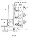
- Figure 1 is a block diagram of an example of a display system ofpresent invention;
- Figure 2 is a simplified diagram of an interface of the displaysystem of Figure 1;
- Figure 3 is a block diagram of a video source of the display systemof Figure 1;
- Figure 4 is a block diagram of a display device of the displaysystem of Figure 1; and,
- Figure 5 is a flow diagram corresponding to the display system ofFigure 1.
- Referring first to Figure 1, an example of a display system of thepresent invention comprises a
digital display device 10 such as a liquidcrystal display, projection display, cathode ray tube display, or thelike. Acomputer system unit 20 such as a personal computer, work-station.or the like, has an internal video output sub-system connectedto displaydevice 10 via aninterface 50. Input devices, including akeyboard 30 andpointing device 40 are connected to data input ports ofsystem unit 20. Pointing device may be in the form of a mouse, trackerball, joystick, touch-screen, or the like.System unit 20 comprises acentral processing unit (CPU) such as a microprocessor, memory, and massdata storage means such as a hard disk drive all interconnected by a busarchitecture. Bus architecture further extends to the video sub-system,the data input ports, and additional data output ports for connection to,for example, a printer. In operation, CPU executes computer program codestored in the memory or retrieved from the mass storage means to produce,via the video sub-system, digital video signals fordriving displaydevice 10 to generate a visual output. A user can control execution ofthe program code by the CPU viakeyboard 30 and pointingdevice 40. - Referring to Figure 2,
interface 50 comprises: Red, Green, and Bluedigital video channels R, G , and B; a timing channel TC; and, a controlchannel I. - Referring now to Figure 3, the video sub-system of
system unit 20comprises a colourdigital output palette 200 having an N bit video dataoutput, a pixel clock output CLK, a data valid output DV, and line andframe sync outputs Hsync and Vsync. The N bit video data output is connectedto an N X Ncross-point switch 210. Sync outputs Hsync and Vsync and pixelclock output CLK provide inputs to asumming logic block 240. The output ofsumming block 240 provides timing channel TC ofinterface 50. Theoutput ofcross-point 210 is connected to each of three parallel inputserial output shift registers 260-262. Each of registers 260-262 hasphase locked loop and counter logic 270-271. The data valid output ofpalette 200 is connected to an enable input of each of registers 260-262.The serial output of each register 260-262 is connected, via a bufferamplifier 250-252, to a different one of video channels R, G, and B ofinterface 50. Each channel R, G, and B corresponds to a different one ofthe three primary colours Red, Green and Blue. Control channel I ofinterface cable 50 is connected to acommunications logic block 230. Acontrol logic block 220 is coupled tologic block 230 andpalette 200.Control logic block 220 has three control outputs BPP Cntl each 4 bitswide and each connected to a different one of phase locked loop andcounter logic blocks 270-272. The pixel clock output CLK fromPalette 200is also connected to each of logic blocks 270-272. - In operation, data to be displayed on
display device 10 is writtenby the CPU ofsystem unit 20 to a video memory (not shown) of the videosub-system. The data stored in the video memory is converted bypalette 200 into a colour data set for each pixel of the image to be displayed ondisplay device 10. The pixel data set corresponding to each pixel ispresented in parallel at the output ofpalette 200 as an N bit wide word.Data valid signal DV is generated bypalette 200 shortly thereafter toindicate that the N bit word has stabilised. Each of the primary coloursfor a pixel is represented by a different sub-set of bits of thecorresponding N bit word. Thus all three colours are presentedsimultaneously. For example, the N bit word may be 16 bits wide and theRed, Green and Blue colour data may be 5, 6, and 5 bits widerespectively.Palette 200 also generates a pixel clock signal CLKsynchronised to presentation of each N bit word. - Each N bit word is routed, via
cross point switch 210, to registers260-262. The operation ofcross point switch 210 will be described indetail shortly. Specifically, the red colour data is routed to register260; the green colour data is routed to register 261; and the blue colourdata is routed to register 262. Each colour data subset is loaded intothe corresponding register in parallel in response to data valid signalDV. Each register 260-262 acts as a serialiser. Specifically, eachregister sequentially sends bits of colour data along the correspondingvideo channel to displaydevice 10. The rate of transmission of bits fromeach register 260-262 to displaydevice 10 is higher than the pixel clock by a factor equal to the number of bits constituting the correspondingcolour data. The rate of transmission from the shift register iscontrolled by a shift register clock. The shift register clock isgenerated by the corresponding phase locked loop and counter logic 270-272.The corresponding phase locked loop and counter logic multipliespixel clock signal CLK by the number of bits constituting thecorresponding colour data to generate the shift register clock. Eachcolour data is thus transmitted at the shift register clock frequency ofthe corresponding register 260-262. The phase locked loop and counterlogic 270-272 of each register 260-262 is programmed with a correspondingbits per pixel value BPP Cntl bycontrol logic block 220. in the Figure 3arrangement, each BPP Cntl value is allocated 4 bits. This allows amaximum of 16 states or 15 bits per pixel (where a value 0 effectivelydisables the corresponding channel). 15 bits per pixel permits 32768shades of a single primary colour or a maximum of 245 = 3.5 x 10¹³ coloursfor an individual pixel. Such level of variation is greater than thatresolvable by the human eye. - In modification to the Figure 3 arrangement, there is providederror logic for producing a parity bit, CRC checksum, or other error codefor permitting error detection. The error code is sent with the pixeldata and decoded in
display device 10. It will be appreciated thatdisplay device 10 may, in turn comprise error correction logic forcorrecting received data based on the decoded error code. - Summing
logic 240 sums sync signals Hsync and Vsync and pixel clocksignal CLK (or at least a sub-multiple thereof) to generate a compositetiming signal on timing channel TC ofinterface 50. In preferredembodiments of the present invention, pixel clock signal CLK is filteredto reduce high frequency content and reduced in amplitude prior tosummation to minimise potential for electro-magnetic interference. - Referring now to Figure 4,
display device 10 comprises acommunications logic block 100 connected to control channel I ofinterface 50.Communications logic block 100 is connected to adisplayprocessor 120 ofdisplay device 10 and acontrol logic block 110. Thered, green and blue video channels R, G, and B ofinterface 50 are eachconnected, via a buffer amplifier 140-142, to a different one of a groupof three serial input parallel output shift registers 150-152. Each ofregisters 150-152 comprises phase locked loop and counter logic 160-162.Control logic block 110 has three control outputs each 4 bits wide and each connected to different one of phase locked loop and control logic160-162. Each register 150-152 has a data valid output DV' in addition toa parallel colour data output R', G' and B'. Timing channel TC ofinterface 50 is connected to a timingseparation logic block 130 having apixel clock output CLK' and line and frame sync outputs Hsync' andVsync'. Pixel clock output CLK' is connected to the each of logic blocks160-162. - In operation, buffer amplifiers 140-142 receive serial colour databits for each pixel from the corresponding video channels R, G, and B.The received data bits are delivered by buffer amplifiers 140-142 to theserial inputs of the corresponding registers 150-152.
Sync separatorlogic 130 separates line and frame sync signals Hsync and Vsync from thecomposite signal on timing channel TC ofinterface 50.Separator logic 130 also includes clock recovery logic for recovering pixel clock signalCLK' from the composite timing signal. The bits per pixel value for eachvideo channel is recovered bycommunications logic 100 from controlchannel I ofinterface 50.Communication logic 100 supplies the bits perpixel values to controllogic 110.Control logic 110 programmes phaselocked loop and counter logic 160-162 of registers 150-152 as a functionof the received bits per pixel values. Each register 150-152 sequentiallyloads bits of colour data from the corresponding video channel R, G, andB. The rate of reception of bits by each register 150-152 is higher thanrecovered pixel clock CLK' by a factor equal to the number of bitsconstituting the corresponding colour data. The rate of reception by theregister 150-152 is controlled by a shift register clock. The shiftregister clock is generated by the corresponding phase locked loop andcounter logic 160-162. The corresponding phase locked loop and counterlogic 160-162 multiplies recovered pixel clock signal CLK' by the numberof bits constituting the corresponding colour data to generate the shiftregister clock. Each colour data is thus received at the shift registerclock frequency of the corresponding register 150-152. As mentionedabove, the phase locked loop and counter logic 160-162 of each register150-152 is programmed with a corresponding bits per pixel value bycontrol logic block 110. Thus the colour data P', G', and B' is presentedat the parallel output of the corresponding registers 160-162'simultaneously thereby reconstructing the N bit pixel data word. Eachregister 150-152 generates a data valid signal DV' to indicate that thecorresponding colour data at the parallel output of the register 150-152has stabilised. It will be appreciated that each register 150-152 acts asa deserialiser. - Referring now to Figure 5, a preferred initialisation sequence forthe examples of the present invention hereinbefore described commences in
system unit 20 by the video sub-system disabling timing channel TC. Indisplay device 10, the sequence commences withdisplay processor 120resetting the display drive circuitry and then waiting for a command fromsystem unit 10. with the timing channel disabled, the video sub-systemthen sends a token to thedisplay device 10 via control channel I ofinterface 50 and waits for display device to return the token, again viacontrol channel I. If, after a predetermined period of time the videosub-system has yet to receive the token fromdisplay device 10, the videosub-system send another token. On receipt of the token from thedisplaydevice 10, the video sub-system sends a RESET instruction to displaydevice 10.Display Device 10 responds to the RESET instruction byresetting the display drive circuitry and by sending video sub-systemperformance data, indicative of the operating parameters ofdisplaydevice 10, via control channel I. Specifically the performance datacomprises pixel addressability (or resolution) ADDR; maximum REFRESHrate; and maximum BPP (bits per pixel) for each video channel R, G, andB. Display device 10 then waits for the next command from the video sub-system.The video sub-system reads the performance data sent bydisplaydevice 10. If the addressability value received fromdisplay device 10,DISPLAY ADDR is less than the addressability value currently retained bythe video sub-system, PC ADDR, then the video sub-system sets PC ADDR toDISPLAY ADDR. Otherwise, the video sub-system sets PC ADDR to maximum. Ifthe refresh rate, PC REFRESH, stored in the video sub-system is greaterthan the refresh rate, DISPLAY REFRESH, received fromdisplay device 10,then the video sub-system sets PC REFRESH to less than or equal toDISPLAY REFRESH. Furthermore, for each video channel R, G, and B, if thecorresponding bits per pixel value received fromdisplay device 10,DISPLAY BPP is less than the corresponding bits per pixel value stored bythe video sub-system, PC BPP, then the video sub-system sets PC BPP toDISPLAY BPP. Otherwise, the video sub-system sets PC BPP to maximum. Thevideo sub-system then sends the bits per pixel value, PC BPP, for eachvideo channel R, G, and B, to displaydevice 10 via control channel r. Ashereinbefore described, on receipt of the bits per pixel valuescorresponding to video channels R, G, and B,display device 10 programsthe phase locked loop and counter logic 160-162 of each register 150-152in preparation to receive video data streams from the video sub-system.Display processor 120 then sets a STATUS code to indicate thatdisplaydevice 10 is ready for operation.Display device 10 then waits for thenext command from the video sub-system. After sending the bits per pixel values to displaydevice 10, the video sub-system turns on timing channelTC and reads the STATUS code fromdisplay device 10. The above describedsequence of events is the same insystem unit 20 for power on, re-boot,and display resolution mode changes. Indisplay device 10, the abovesequence of events is the same for power on and return from a stand-by(eg: power management) state. - Note that the above initialisation sequence allows the video sub-systemand
display device 10 to have different abilities. The sequenceselects the highest mode of operation common to bothdisplay device 10and the video sub-system. It will be appreciated that any other commonmode may also be selected by appropriate programming of the video sub-system. - It will be appreciated that embodiments of the present inventionhereinbefore described with reference to Figure 5 are essentiallymaster/slave systems in which
system unit 20 is always the master. Thesame initialisation sequence is always followed when a new mode ofoperation is required, thereby simplifying programming ofsystem unit 20.It will be appreciated that the above initialisation sequence permitsautomatic configuration of the display system independently of whetherany operating system or graphic drivers are loaded intosystem unit 20. - Returning now to Figure 2, each of channels I, R, G, B and TC of
interface 50 may be formed from any of twisted pair cable, coaxial cable,plastic optical fibre, or glass optical fibre. However, the former threeare generally only suitable for use over relatively short distances (eg:less than 10 m). Beyond such distances, signal degradation tends toadversely affect performance of the display system. In some embodimentsof the present invention, each of video channels R, G, and B may beimplemented ininterface 50 by a separate path (eg: wire or fibre).However, in other embodiments of the present invention, a single path maybe employed by all of video channels R, G and B with each channeloccupying a different portion of the bandwidth of the transmission mediaand transducers forming the path. In the embodiments of the presentinvention hereinbefore described, the speed of transfer of video data viainterface 50 may be 15 times greater than the pixel clock speed. In someembodiments of the present invention, the transmission media employed invideo channels R, G, and B may differ from that employed in timingchannel TC. for example, video channels R, G and B may be implemented byoptical fibre and timing channel TC may be implemented by coax. A problem with such arrangements is that the different transmission media havedifferent propagation velocities. The difference in propagation velocityleads to a phase error atdisplay device 10. There is maximum permissiblephase error beyond which the original digital video data cannot berecovered bydisplay device 10. The maximum phase error is divided by therelative frequencies of the digital video data and the timing data. Thus,by way of example, for digital video pixel data transmitted with 8 bitsof colour information and 1 parity bit, the maximum phase error isreduced from 90 degrees to 10 degrees. It will be appreciated therefore,that in a preferred embodiment of the present invention, the sametransmission medium is employed for transport of both video and timingdata in the interests of preventing skewing between the two. In aparticularly preferred embodiment of the present invention, the video andtiming data are transmitted over a single optical fibre. - Referring back to Figure 3, as mentioned earlier, in someapplications,
palette 200 may vary the logical width of the N bit word toprovide a different number of bits per pixel as required.Cross pointswitch 210 permit reorganisation of signal routing betweenpalette 200and registers 260-262 to accommodate different numbers of bits per pixeland, in particular, to ensure colour data is routed to the appropriateregisters 260-262. It will be appreciated that such re-organisation mayinvolve presentation of data corresponding to more than 1 pixel toregisters 260-262 simultaneously. Cross-point 210 also permits reorderingof pixel data to swap the order in which data is sent to displaydevice 10 from, for example, least significant bit first to mostsignificant bit first, or vice versa. Furthermore, cross-point 210permits routing of colour data to only one or two video channels insteadof all three channels to allow for example communications over a singlepath, or to maintain communications in the event of failure of one ormore channels. It will be appreciated that, in some embodiments of thepresent invention,cross-point switch 210 may be omitted. - Examples of the present invention have been hereinbefore describedwith reference to a colour digital display device. It will however beappreciated that the present invention is equally applicable to displaysystems including monochrome digital display devices.
- in the embodiments of the present invention, hereinbeforedescribed, the data stored in the video memory is converted by
palette 200 into a colour data set for each pixel of the image to be displayed ondisplay device 10. However, it will be appreciated that other embodimentsmay be operable in a direct colour mode in which colour data stored inthe video memory is transferred directly to the N bit output ofpalette 200.
Claims (12)
- Apparatus for generating a serial video bit stream, the apparatus (20)comprising: a pixel clock generator (200) for generating a pixel clock signal CLK;palette logic (200) for generating a pixel data word N on each pulse of the pixelclock signal; shift clock generator logic (270, 271, 272) for multiplying the pixel clocksignal by the number of bits N in the pixel data word to produce a shiftclock signal; and, serialiser logic (260, 261, 262) for serially outputting the pixel data word ina serial bit stream at the shift clock signal rate.
- Apparatus as claimed in claim 1, comprising control logic connectedto the shift clock generator logic for reading the number of bits in thepixel data word from an external source.
- Apparatus as claimed in claim 1 or claim 2, comprising cross-pointswitch logic for transferring the pixel data word generated by thepalette logic to the serialiser logic.
- Apparatus as claimed in any preceding claim, comprising error logicfor generating an error code corresponding to the pixel data word and foradding the error code to the serial bit stream.
- Display apparatus comprising: a display screen (10) for producing apixel of an image at least partially in response to a pixel data word; a timing recever (130) forreceiving a pixel clock signal CLK' from an external video source (20) shift clockgenerator logic (160, 161, 162) for multiplying the pixel clock signal by the number ofbits N in the pixel word to produce a shift clock signal; and, deserialiserlogic (150, 151, 152) for receiving an input video bit stream at the shift clock signalrate to generate the pixel word.
- Apparatus as claimed in claim 5, comprising control logic connectedto the shift clock generator logic for reading the number of bits in thepixel data word from an external source.
- Apparatus as claimed in claim 5 or claim 6, comprising error logicfor detecting an error in the pixel word and from an error code in theserial bit stream.
- Apparatus as claimed in any of claims 5 to 7, wherein the pixelword defines a pixel of a monochrome video image.
- Apparatus as claimed in any of claims 5 to 7, wherein the pixelword defines a colour component of a pixel of a colour video image.
- A display system comprising a digital video source (20) coupled to adigital display device (10) via a digital interface (50) having a timing channel TCfor carrying a pixel clock signal CLK from the video source to the displaydevice and a digital video channel RGB for carrying a digital video bitstream from the video source to the display device, wherein the videosource (20) comprises a pixel clock generator (200) for generating the pixel clocksignal CLK, palette logic (200) for outputting a pixel data word N on each pulse of thepixel clock signal, first shift clock generator logic (270, 271, 272) for mutiplying the pixelclock signal by the number of bits N in the pixel word to produce a shiftclock signal, and serialiser logic (260, 261, 262) for serially outputting the pixel data wordin the serial bit stream at the shift clock signal rate, and wherein thedisplay device (10) comprises a display screen (10) for producing a pixel of animage at least partially in response to the pixel data word; a timing receiver (130) for receiving a pixel clock signal CLK' from the video source (20); second shift clock generator logic (160, 161, 162) formultiplying the pixel clock signal by the number of bis N in the pixelword, and deserialiser logic (150, 151, 152) for receiving the input video bit stream atthe shift clock signal rate to re-generate the pixel word from the videobit stream.
- A display system as claimed in claim 10, wherein the interfacecomprises a control channel for communicating the number of bits in thepixel word from the video source to the display device.
- A computer system comprising a processor, a memory, and a displaysystem as claimed in claim 10 or claim 11.
Applications Claiming Priority (2)
| Application Number | Priority Date | Filing Date | Title |
|---|---|---|---|
| GB9602293 | 1996-02-05 | ||
| GB9602293AGB2309872A (en) | 1996-02-05 | 1996-02-05 | Digital display apparatus |
Publications (2)
| Publication Number | Publication Date |
|---|---|
| EP0788048A1 EP0788048A1 (en) | 1997-08-06 |
| EP0788048B1true EP0788048B1 (en) | 2003-06-04 |
Family
ID=10788135
Family Applications (1)
| Application Number | Title | Priority Date | Filing Date |
|---|---|---|---|
| EP97300289AExpired - LifetimeEP0788048B1 (en) | 1996-02-05 | 1997-01-17 | Display apparatus interface |
Country Status (5)
| Country | Link |
|---|---|
| US (1) | US5963193A (en) |
| EP (1) | EP0788048B1 (en) |
| JP (1) | JP3352600B2 (en) |
| DE (1) | DE69722476T2 (en) |
| GB (1) | GB2309872A (en) |
Cited By (17)
| Publication number | Priority date | Publication date | Assignee | Title |
|---|---|---|---|---|
| US7567592B2 (en) | 2003-05-01 | 2009-07-28 | Genesis Microchip Inc. | Packet based video display interface enumeration method |
| US7613300B2 (en) | 2003-09-26 | 2009-11-03 | Genesis Microchip Inc. | Content-protected digital link over a single signal line |
| US7620062B2 (en) | 2003-05-01 | 2009-11-17 | Genesis Microchips Inc. | Method of real time optimizing multimedia packet transmission rate |
| US7634090B2 (en) | 2003-09-26 | 2009-12-15 | Genesis Microchip Inc. | Packet based high definition high-bandwidth digital content protection |
| US7733915B2 (en) | 2003-05-01 | 2010-06-08 | Genesis Microchip Inc. | Minimizing buffer requirements in a digital video system |
| US7839860B2 (en) | 2003-05-01 | 2010-11-23 | Genesis Microchip Inc. | Packet based video display interface |
| US8068485B2 (en) | 2003-05-01 | 2011-11-29 | Genesis Microchip Inc. | Multimedia interface |
| US8156238B2 (en) | 2009-05-13 | 2012-04-10 | Stmicroelectronics, Inc. | Wireless multimedia transport method and apparatus |
| US8204076B2 (en) | 2003-05-01 | 2012-06-19 | Genesis Microchip Inc. | Compact packet based multimedia interface |
| US8291207B2 (en) | 2009-05-18 | 2012-10-16 | Stmicroelectronics, Inc. | Frequency and symbol locking using signal generated clock frequency and symbol identification |
| US8370554B2 (en) | 2009-05-18 | 2013-02-05 | Stmicroelectronics, Inc. | Operation of video source and sink with hot plug detection not asserted |
| US8429440B2 (en) | 2009-05-13 | 2013-04-23 | Stmicroelectronics, Inc. | Flat panel display driver method and system |
| US8468285B2 (en) | 2009-05-18 | 2013-06-18 | Stmicroelectronics, Inc. | Operation of video source and sink with toggled hot plug detection |
| US8582452B2 (en) | 2009-05-18 | 2013-11-12 | Stmicroelectronics, Inc. | Data link configuration by a receiver in the absence of link training data |
| US8671234B2 (en) | 2010-05-27 | 2014-03-11 | Stmicroelectronics, Inc. | Level shifting cable adaptor and chip system for use with dual-mode multi-media device |
| US8760461B2 (en) | 2009-05-13 | 2014-06-24 | Stmicroelectronics, Inc. | Device, system, and method for wide gamut color space support |
| US8860888B2 (en) | 2009-05-13 | 2014-10-14 | Stmicroelectronics, Inc. | Method and apparatus for power saving during video blanking periods |
Families Citing this family (24)
| Publication number | Priority date | Publication date | Assignee | Title |
|---|---|---|---|---|
| US20030030618A1 (en)* | 1999-02-26 | 2003-02-13 | Morris Jones | Method and apparatus for sensing changes in digital video data |
| US7023442B2 (en)* | 2000-06-28 | 2006-04-04 | Sun Microsystems, Inc. | Transferring a digital video stream through a series of hardware modules |
| KR100365497B1 (en)* | 2000-12-15 | 2002-12-18 | 엘지.필립스 엘시디 주식회사 | Liquid Crystal Display and Driving Method Thereof |
| SE522004C2 (en)* | 2001-05-09 | 2004-01-07 | Comex Electronics Ab | Method and apparatus for reducing the presence of clearing signals from a keyboard |
| KR100402409B1 (en)* | 2001-05-26 | 2003-10-30 | (주)오피트정보통신 | Digital Vidio Signal Interface Module For Transmitting Long Distance |
| WO2003019318A2 (en)* | 2001-08-27 | 2003-03-06 | Koninklijke Philips Electronics N.V. | Processing module for a computer system device |
| US7327355B2 (en)* | 2001-12-08 | 2008-02-05 | Samsung Electronics Co., Ltd. | LCD monitor with dual interface and control method thereof |
| US7653315B2 (en)* | 2003-01-21 | 2010-01-26 | Gateway, Inc. | Bi-directional optical monitor interconnect |
| US7405719B2 (en) | 2003-05-01 | 2008-07-29 | Genesis Microchip Inc. | Using packet transfer for driving LCD panel driver electronics |
| US20040218599A1 (en)* | 2003-05-01 | 2004-11-04 | Genesis Microchip Inc. | Packet based video display interface and methods of use thereof |
| US7424558B2 (en) | 2003-05-01 | 2008-09-09 | Genesis Microchip Inc. | Method of adaptively connecting a video source and a video display |
| US8059673B2 (en) | 2003-05-01 | 2011-11-15 | Genesis Microchip Inc. | Dynamic resource re-allocation in a packet based video display interface |
| US7487273B2 (en) | 2003-09-18 | 2009-02-03 | Genesis Microchip Inc. | Data packet based stream transport scheduler wherein transport data link does not include a clock line |
| US7800623B2 (en) | 2003-09-18 | 2010-09-21 | Genesis Microchip Inc. | Bypassing pixel clock generation and CRTC circuits in a graphics controller chip |
| KR20050096701A (en)* | 2004-03-31 | 2005-10-06 | (주)오피트정보통신 | Digital visual transmmiter |
| JP2005316146A (en)* | 2004-04-28 | 2005-11-10 | Fujitsu Display Technologies Corp | Liquid crystal display device and processing method thereof |
| US7705842B2 (en)* | 2006-01-11 | 2010-04-27 | Microsoft Corporation | Fast display initialization and light up |
| US7903047B2 (en)* | 2006-04-17 | 2011-03-08 | Qualcomm Mems Technologies, Inc. | Mode indicator for interferometric modulator displays |
| US7917442B2 (en)* | 2006-09-21 | 2011-03-29 | Sony Corporation | System and method for relaxing media access restrictions over time |
| US9036081B2 (en) | 2007-11-30 | 2015-05-19 | Thine Electronics, Inc. | Video signal transmission device, video signal reception device, and video signal transmission system |
| JP4805900B2 (en)* | 2007-11-30 | 2011-11-02 | ザインエレクトロニクス株式会社 | Video signal transmitting apparatus, video signal receiving apparatus, and video signal transmission system |
| US20110048488A1 (en)* | 2009-09-01 | 2011-03-03 | Gabriel Karim M | Combined thermoelectric/photovoltaic device and method of making the same |
| US20110048489A1 (en)* | 2009-09-01 | 2011-03-03 | Gabriel Karim M | Combined thermoelectric/photovoltaic device for high heat flux applications and method of making the same |
| US8788890B2 (en) | 2011-08-05 | 2014-07-22 | Apple Inc. | Devices and methods for bit error rate monitoring of intra-panel data link |
Family Cites Families (10)
| Publication number | Priority date | Publication date | Assignee | Title |
|---|---|---|---|---|
| US4827255A (en)* | 1985-05-31 | 1989-05-02 | Ascii Corporation | Display control system which produces varying patterns to reduce flickering |
| US5384912A (en)* | 1987-10-30 | 1995-01-24 | New Microtime Inc. | Real time video image processing system |
| US5543819A (en)* | 1988-07-21 | 1996-08-06 | Proxima Corporation | High resolution display system and method of using same |
| JP2865676B2 (en)* | 1988-10-05 | 1999-03-08 | 株式会社日立製作所 | Image display device |
| US5296851A (en)* | 1990-06-08 | 1994-03-22 | Mita Industrial Co., Ltd. | Signal communication system |
| US5293468A (en)* | 1990-06-27 | 1994-03-08 | Texas Instruments Incorporated | Controlled delay devices, systems and methods |
| FR2664765B1 (en)* | 1990-07-11 | 2003-05-16 | Bull Sa | DEVICE FOR SERIALIZATION AND DESERIALIZATION OF DATA AND SYSTEM FOR DIGITAL TRANSMISSION OF SERIAL DATA THEREOF. |
| US5107264A (en)* | 1990-09-26 | 1992-04-21 | International Business Machines Corporation | Digital frequency multiplication and data serialization circuits |
| US5621425A (en)* | 1992-12-24 | 1997-04-15 | Seiko Instruments Inc. | Liquid crystal display device |
| JP3259428B2 (en)* | 1993-03-24 | 2002-02-25 | ソニー株式会社 | Apparatus and method for concealing digital image signal |
- 1996
- 1996-02-05GBGB9602293Apatent/GB2309872A/ennot_activeWithdrawn
- 1996-10-15USUS08/732,804patent/US5963193A/ennot_activeExpired - Lifetime
- 1997
- 1997-01-17EPEP97300289Apatent/EP0788048B1/ennot_activeExpired - Lifetime
- 1997-01-17DEDE69722476Tpatent/DE69722476T2/ennot_activeExpired - Lifetime
- 1997-01-21JPJP00819097Apatent/JP3352600B2/ennot_activeExpired - Lifetime
Cited By (19)
| Publication number | Priority date | Publication date | Assignee | Title |
|---|---|---|---|---|
| US8204076B2 (en) | 2003-05-01 | 2012-06-19 | Genesis Microchip Inc. | Compact packet based multimedia interface |
| US8068485B2 (en) | 2003-05-01 | 2011-11-29 | Genesis Microchip Inc. | Multimedia interface |
| US7620062B2 (en) | 2003-05-01 | 2009-11-17 | Genesis Microchips Inc. | Method of real time optimizing multimedia packet transmission rate |
| US7567592B2 (en) | 2003-05-01 | 2009-07-28 | Genesis Microchip Inc. | Packet based video display interface enumeration method |
| US7733915B2 (en) | 2003-05-01 | 2010-06-08 | Genesis Microchip Inc. | Minimizing buffer requirements in a digital video system |
| US7839860B2 (en) | 2003-05-01 | 2010-11-23 | Genesis Microchip Inc. | Packet based video display interface |
| US7634090B2 (en) | 2003-09-26 | 2009-12-15 | Genesis Microchip Inc. | Packet based high definition high-bandwidth digital content protection |
| US7613300B2 (en) | 2003-09-26 | 2009-11-03 | Genesis Microchip Inc. | Content-protected digital link over a single signal line |
| US8385544B2 (en) | 2003-09-26 | 2013-02-26 | Genesis Microchip, Inc. | Packet based high definition high-bandwidth digital content protection |
| US8156238B2 (en) | 2009-05-13 | 2012-04-10 | Stmicroelectronics, Inc. | Wireless multimedia transport method and apparatus |
| US8860888B2 (en) | 2009-05-13 | 2014-10-14 | Stmicroelectronics, Inc. | Method and apparatus for power saving during video blanking periods |
| US8760461B2 (en) | 2009-05-13 | 2014-06-24 | Stmicroelectronics, Inc. | Device, system, and method for wide gamut color space support |
| US8429440B2 (en) | 2009-05-13 | 2013-04-23 | Stmicroelectronics, Inc. | Flat panel display driver method and system |
| US8788716B2 (en) | 2009-05-13 | 2014-07-22 | Stmicroelectronics, Inc. | Wireless multimedia transport method and apparatus |
| US8370554B2 (en) | 2009-05-18 | 2013-02-05 | Stmicroelectronics, Inc. | Operation of video source and sink with hot plug detection not asserted |
| US8582452B2 (en) | 2009-05-18 | 2013-11-12 | Stmicroelectronics, Inc. | Data link configuration by a receiver in the absence of link training data |
| US8468285B2 (en) | 2009-05-18 | 2013-06-18 | Stmicroelectronics, Inc. | Operation of video source and sink with toggled hot plug detection |
| US8291207B2 (en) | 2009-05-18 | 2012-10-16 | Stmicroelectronics, Inc. | Frequency and symbol locking using signal generated clock frequency and symbol identification |
| US8671234B2 (en) | 2010-05-27 | 2014-03-11 | Stmicroelectronics, Inc. | Level shifting cable adaptor and chip system for use with dual-mode multi-media device |
Also Published As
| Publication number | Publication date |
|---|---|
| DE69722476D1 (en) | 2003-07-10 |
| GB2309872A (en) | 1997-08-06 |
| US5963193A (en) | 1999-10-05 |
| JPH09218676A (en) | 1997-08-19 |
| GB9602293D0 (en) | 1996-04-03 |
| EP0788048A1 (en) | 1997-08-06 |
| DE69722476T2 (en) | 2004-04-15 |
| JP3352600B2 (en) | 2002-12-03 |
Similar Documents
| Publication | Publication Date | Title |
|---|---|---|
| EP0788048B1 (en) | Display apparatus interface | |
| US6646645B2 (en) | System and method for synchronization of video display outputs from multiple PC graphics subsystems | |
| EP0665527B1 (en) | Flat panel display interface for a high resolution computer graphics system | |
| KR100737000B1 (en) | Data transfer control device and electronic instrument | |
| JP3786120B2 (en) | Data transfer control device and electronic device | |
| US6877106B2 (en) | Image display method, image display system, host device, image display device and display interface | |
| US7307644B2 (en) | Method and system for efficient interfacing to frame sequential display devices | |
| US20070260802A1 (en) | Data transfer control device and electronic instrument generating interface signal of signal type according to interface information set in internal register | |
| US20010030649A1 (en) | Method for displaying image, image display system, host system, image display apparatus, and interface for display | |
| EP1519349A2 (en) | Bypassing pixel clock generation and CRTC circuits in a graphics controller chip | |
| US6816131B2 (en) | Single horizontal scan range CRT monitor | |
| JPH0827705B2 (en) | adapter | |
| US11936927B2 (en) | Transmission control system of multi-media signal, transmitter control circuit and receiver control circuit | |
| US20050165994A1 (en) | Signal transmission over a wire pair | |
| CA2372109C (en) | Apparatus and method for merging pixels | |
| US5859635A (en) | Polarity synchronization method and apparatus for video signals in a computer system | |
| JP3481868B2 (en) | Data transmission circuit and liquid crystal display device | |
| JP3786121B2 (en) | Data transfer control device and electronic device | |
| US6822637B2 (en) | Apparatus, method and program for generating image signal having pointer signal | |
| JPH09274475A (en) | A plurality of display devices capable of connecting to one computer | |
| JP2004347739A (en) | Daisy chain circuit, display device, and multi-display system | |
| KR20010100617A (en) | Computer display apparatus | |
| JPH0981081A (en) | Liquid crystal display system | |
| TW202343221A (en) | Docking display | |
| JPH1195713A (en) | Connection circuit between external image equipment and liquid crystal panel part |
Legal Events
| Date | Code | Title | Description |
|---|---|---|---|
| PUAI | Public reference made under article 153(3) epc to a published international application that has entered the european phase | Free format text:ORIGINAL CODE: 0009012 | |
| AK | Designated contracting states | Kind code of ref document:A1 Designated state(s):DE FR GB | |
| 17P | Request for examination filed | Effective date:19980113 | |
| GRAH | Despatch of communication of intention to grant a patent | Free format text:ORIGINAL CODE: EPIDOS IGRA | |
| GRAH | Despatch of communication of intention to grant a patent | Free format text:ORIGINAL CODE: EPIDOS IGRA | |
| GRAA | (expected) grant | Free format text:ORIGINAL CODE: 0009210 | |
| AK | Designated contracting states | Designated state(s):DE FR GB | |
| REG | Reference to a national code | Ref country code:GB Ref legal event code:FG4D | |
| REF | Corresponds to: | Ref document number:69722476 Country of ref document:DE Date of ref document:20030710 Kind code of ref document:P | |
| ET | Fr: translation filed | ||
| PLBE | No opposition filed within time limit | Free format text:ORIGINAL CODE: 0009261 | |
| STAA | Information on the status of an ep patent application or granted ep patent | Free format text:STATUS: NO OPPOSITION FILED WITHIN TIME LIMIT | |
| 26N | No opposition filed | Effective date:20040305 | |
| REG | Reference to a national code | Ref country code:GB Ref legal event code:746 Effective date:20081215 | |
| REG | Reference to a national code | Ref country code:FR Ref legal event code:TP Owner name:GOOGLE INC., US Effective date:20120314 | |
| REG | Reference to a national code | Ref country code:GB Ref legal event code:732E Free format text:REGISTERED BETWEEN 20120503 AND 20120509 | |
| REG | Reference to a national code | Ref country code:DE Ref legal event code:R085 Ref document number:69722476 Country of ref document:DE Effective date:20120316 | |
| REG | Reference to a national code | Ref country code:GB Ref legal event code:S47 Free format text:CANCELLATION OF ENTRY; APPLICATION BY FILING PATENTS FORM 15 WITHIN 4 WEEKS FROM THE DATE OF PUBLICATION OF THIS JOURNAL GOOGLE, INC DISPLAY APPARATUS INTERFACE APPLICATION BY PROPRIETOR TO CANCEL LICENCE OF RIGHT UNDER SECTION 47(1) FILED ON 9 MARCH 2012. | |
| REG | Reference to a national code | Ref country code:DE Ref legal event code:R082 Ref document number:69722476 Country of ref document:DE Representative=s name:PFENNING MEINIG & PARTNER GBR, DE | |
| REG | Reference to a national code | Ref country code:DE Ref legal event code:R082 Ref document number:69722476 Country of ref document:DE Representative=s name:WUESTHOFF & WUESTHOFF, PATENTANWAELTE PARTG MB, DE Effective date:20120717 Ref country code:DE Ref legal event code:R082 Ref document number:69722476 Country of ref document:DE Representative=s name:PFENNING MEINIG & PARTNER GBR, DE Effective date:20120717 Ref country code:DE Ref legal event code:R081 Ref document number:69722476 Country of ref document:DE Owner name:GOOGLE INC., US Free format text:FORMER OWNER: INTERNATIONAL BUSINESS MACHINES CORP., ARMONK, US Effective date:20120717 Ref country code:DE Ref legal event code:R081 Ref document number:69722476 Country of ref document:DE Owner name:GOOGLE INC., MOUNTAIN VIEW, US Free format text:FORMER OWNER: INTERNATIONAL BUSINESS MACHINES CORPORATION, ARMONK, N.Y., US Effective date:20120717 | |
| REG | Reference to a national code | Ref country code:GB Ref legal event code:S47 Free format text:ENTRY CANCELLED; NOTICE IS HEREBY GIVEN THAT THE ENTRY ON THE REGISTER 'LICENCES OF RIGHT' UPON THE UNDERMENTIONED PATENT WAS CANCELLED ON 12 OCTOBER 2012 GOOGLE INC DISPLAY APPARATUS INTERFACE | |
| REG | Reference to a national code | Ref country code:DE Ref legal event code:R082 Ref document number:69722476 Country of ref document:DE Representative=s name:WUESTHOFF & WUESTHOFF, PATENTANWAELTE PARTG MB, DE | |
| REG | Reference to a national code | Ref country code:FR Ref legal event code:PLFP Year of fee payment:20 | |
| PGFP | Annual fee paid to national office [announced via postgrant information from national office to epo] | Ref country code:DE Payment date:20160127 Year of fee payment:20 | |
| PGFP | Annual fee paid to national office [announced via postgrant information from national office to epo] | Ref country code:GB Payment date:20160127 Year of fee payment:20 Ref country code:FR Payment date:20160126 Year of fee payment:20 | |
| REG | Reference to a national code | Ref country code:DE Ref legal event code:R071 Ref document number:69722476 Country of ref document:DE | |
| REG | Reference to a national code | Ref country code:GB Ref legal event code:PE20 Expiry date:20170116 | |
| PG25 | Lapsed in a contracting state [announced via postgrant information from national office to epo] | Ref country code:GB Free format text:LAPSE BECAUSE OF EXPIRATION OF PROTECTION Effective date:20170116 | |
| REG | Reference to a national code | Ref country code:FR Ref legal event code:CJ Effective date:20180213 Ref country code:FR Ref legal event code:CD Owner name:GOOGLE INC., US Effective date:20180213 | |
| P01 | Opt-out of the competence of the unified patent court (upc) registered | Effective date:20230525 |