EP0786921B1 - Digital demodulator - Google Patents
Digital demodulatorDownload PDFInfo
- Publication number
- EP0786921B1 EP0786921B1EP96101105AEP96101105AEP0786921B1EP 0786921 B1EP0786921 B1EP 0786921B1EP 96101105 AEP96101105 AEP 96101105AEP 96101105 AEP96101105 AEP 96101105AEP 0786921 B1EP0786921 B1EP 0786921B1
- Authority
- EP
- European Patent Office
- Prior art keywords
- signal
- phase
- quadrature
- phase signal
- demodulator
- Prior art date
- Legal status (The legal status is an assumption and is not a legal conclusion. Google has not performed a legal analysis and makes no representation as to the accuracy of the status listed.)
- Expired - Lifetime
Links
- 238000012986modificationMethods0.000claimsdescription7
- 230000004048modificationEffects0.000claimsdescription7
- 230000005540biological transmissionEffects0.000description7
- 238000012937correctionMethods0.000description4
- 239000000654additiveSubstances0.000description2
- 230000000996additive effectEffects0.000description2
- 230000000295complement effectEffects0.000description2
- 239000011159matrix materialSubstances0.000description2
- 238000000034methodMethods0.000description2
- 238000012935AveragingMethods0.000description1
- 230000015572biosynthetic processEffects0.000description1
- 238000006243chemical reactionMethods0.000description1
- 230000008878couplingEffects0.000description1
- 238000010168coupling processMethods0.000description1
- 238000005859coupling reactionMethods0.000description1
- 230000007423decreaseEffects0.000description1
- 238000001514detection methodMethods0.000description1
- 238000010586diagramMethods0.000description1
- 230000000694effectsEffects0.000description1
- 238000012545processingMethods0.000description1
- 230000000630rising effectEffects0.000description1
- 230000002123temporal effectEffects0.000description1
- 230000001131transforming effectEffects0.000description1
Images
Classifications
- H—ELECTRICITY
- H04—ELECTRIC COMMUNICATION TECHNIQUE
- H04S—STEREOPHONIC SYSTEMS
- H04S1/00—Two-channel systems
- H04S1/007—Two-channel systems in which the audio signals are in digital form
Definitions
- the inventionrelates to a digital demodulator for a quadrature-modulated signal, which transmits a combination signal by means of amplitude and phase modulation.
- Quadrature modulated signalsare often used when in one Signals belonging to the transmission channel, but which are independent of one another are to be transferred.
- One such applicationis the transmission of Stereo signals according to the C-QUAM standard, in which a sum signal over the Amplitude modulation and a difference signal as well as a pilot tone over the Phase modulation of the respective carrier is transmitted.
- An example of one associated digital demodulatoris published in DE 43 40 012 A1 described.
- a quadrature signal sourceforms from the received one quadrature-modulated signal using a quadrature mixer, an in-phase signal and a Quadrature phase signal. Digitization can take place before or after Quadrature mixer done.
- a coordinate converterBy means of a coordinate converter, in particular according to The Cordic algorithm works from the digitized in-phase signal and the digitized quadrature phase signal, a magnitude signal and a phase signal are formed.
- a control loop controlled by the phase signalcontrols the oscillator frequency of the Quadrature mixer exactly to the value of the carrier frequency, so that the in-phase signal and the quadrature phase signal are transformed into the baseband.
- a remaining average phase deviationis corrected by the control loop also intervenes in the phase signal and adds or subtracts a correction signal there, that pulls the temporal average of the phase signal to the zero phase value.
- Decoderwhich essentially contains a known stereo matrix, forms from the Amount signal and the phase signal, the left and right signal as well as the Pilot signal at 25 Hz.
- the object of the inventionis to provide an improved digital demodulator for such Quadrature modulated signals indicate the better of digital signal processing is adapted and places less demands on the quadrature signal source.
- the main advantage of this arrangementis that the output signals of the Quadrature signal source, the digitized in-phase signal and the digitized Quadrature phase signal do not have to have the exact baseband position, but only must be in a relatively low frequency range.
- the range of this deep Frequency rangedepends on the digitization frequency and should be as possible not be greater than a tenth of the digitization frequency.
- This cheap Boundary conditionsallow that a digital quadrature mixer in the simplest way can be realized by digital switchers because the quadrature modulated digital signal only to be multiplied by the values +1, -1 and 0.
- the first control loopis advantageously controlled via the slope of the first Phase signal resulting from the difference between at least two in time neighboring samples.
- control loopshave one Integrator included. Accumulator loops are particularly suitable for this sufficient job capacity so that there is no overflow in normal operation.
- control signal of the first and / or second control loopis of this type is designed that it as an additive or subtractive correction signal via a Adding circuit can be combined with the respective phase signal.
- the two control signalscan be added combine so that only a single adder for correction in the phase signal path is required.
- the integrator for the first and second Control loopcan be formed together by the two control signals in the adder Accumulator circuit are supplied. Its output then provides the common one Actuating signal.
- the modification devicecorresponds to a predetermined signal characteristic, the inverse to the signal characteristic on the transmitter side.
- the modification devicecan be a have nonlinear characteristics, e.g. is on the C-QUAM standard as a characteristic a tangent curve is prescribed for the receiver side.
- the tangent coursecan be defined by a memory table or by a polynomial approximation as in the DE 43 40 012 already mentioned.
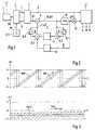
- an input stage 1receives quadrature modulated signal sq from an antenna, cable or other Facility.
- a quadrature signal source 2 with connected oscillator 2.1which as Mixing signal sx emits a digital signal with a predetermined frequency fx an in-phase signal I and a from the quadrature-modulated signal sq Quadrature phase signal Q, both signals I and Q being digitized.
- the Digitizationcan be in the quadrature signal source 2 or already in the Entry level 1 take place.
- C-QUAMCompact - Quadrature Amplitude Modulation
- the amount of this pointershould always assume the value 1 + S, the value 1 representing the carrier with a constant size.
- the size of the difference signal Daffects only the phase position of the pointer M (t).
- a pilot tone P with a frequency of 25 Hzis also applied to the difference signal D.
- 5% modulation modulatedthe stereo detection and thus an automatic Stereo switching enabled.
- the quadrature signal source 2is followed by a coordinate converter 3 which from the in-phase signal I and the quadrature phase signal Q a magnitude signal b and a forms first phase signal p1.
- the coordinate converter 3carries out a conversion from Cartesian coordinates in polar coordinates. Is suitable for this implementation in particular the well-known Cordic algorithm, which uses a iterative approximation determined with arbitrary precision.
- the quadrature mixingit is not necessary for the quadrature mixing to take place directly in the baseband. If the in-phase signal I and the quadrature phase signal Q are sampled at a frequency of 19 kHz, then it is sufficient for the demodulation according to the invention if the remaining rotational frequency ⁇ r of the complex pointer M (t) remains less than 2 kHz.
- the difference between the mixing frequency fx and the carrier frequency fresults in a residual frequency fr and thus a remaining rotational frequency ⁇ r of the complex pointer M (t).
- the first phase signal p1is not constant but increases or decreases constantly over time, cf. also Fig. 2.
- Thiscorresponds to a constant offset frequency ⁇ r which is brought to the value zero by means of a first control circuit 4, in that the mean slope mt of the first phase signal p1 is compensated by a first actuating signal c1 with an equally large negative slope.
- the actuating signal c1is added to the first phase signal p1 by means of a first adder 5 and thus forms a second phase signal p2, cf. also FIG. 3.
- FIG. 3In FIG.
- the slopeis formed by a difference former 6 from two successive sample values, which are then weighted and / or averaged by means of a first filter device 7.
- the output of the first filter device 7is integrated by means of an integrator 8, the output of which supplies the first actuating signal c1 to the first adder 5.
- the difference generator 6consists of a first retarder 6.1 and a subtractor 6.2.
- the integrator 8consists of an accumulator loop with a second adder 8.1 and a second delay 8.2.
- the output signals of the two control loops 4, 9are fed to the second adder 8.1 as inverted signals, so that the control direction in the first adder 5 is correct.
- the compensation of the mean slope mpdoes not cause the second Phase signal p2 comes to lie exactly on the phase reference value on average over time.
- the time average tm of the second phase signal p2is easy in FIG. 3 rising straight line shown below the zero phase reference axis.
- a second control loop 9becomes the time average tm of the second phase signal p2 brought exactly to the zero phase reference axis. This is done by means of a second Filter device 10 and the integrator 8 achieved by the output signal of the first Adders 5 directly or via a modification device 11 to the input of the second Filter device 10 is supplied, at the output of a further input of the Integrators 8 lies.
- the second control circuit 9forms a second control signal c2, that by means of the first adder 5 additive / subtractive to the first Phase signal p1 and a first control signal c1 is added and thus forms a third phase signal p3 that is correct in terms of its slope and phase on average over time.
- phase signal p2supplies the input signal of the second Control loop.
- the current deviations of the third phase signal p3 from the Zero phase reference positionthus only correspond to the searched differential signal D and the pilot signal P.
- the magnitude signals b and the third phase signal p3the sought components L, R, P of the stereo combination signal educated.
- the The third phase signal p3is previously modified using the modification device 11, for example, by determining the associated tangent value. Because in the amount signal b the carrier amplitude is included, that is for the stereo matrix in the decoder 12 third phase signal p3 or the modified phase signal p3 'on the carrier amplitude normalized. This is done by means of a multiplier 13, the first input of which with the Magnitude signal b and its second input with the third phase signal p3 or p3 ' is fed.
- the remaining rotation frequency ⁇ r of the complex pointer M (t)corresponds to a steady increase mp in the middle phase mp1, which is represented by a sawtooth-shaped, solid line.
- the first phase signal p1is preferably represented as a two's complement number whose lower or upper value limit corresponds to the phase angle - ⁇ or + ⁇ .
- the steadily increasing phase mp1thus jumps back from the phase value + ⁇ to the phase value - ⁇ .
- the coupling of the respective phase value to the two's complement number representationhas the great advantage that phase difference values are reproduced correctly, even if the phase has meanwhile overflowed.
- the dashed area around the middle phase mp1indicates the area in which the first phase signal p1 can be due to the modulation with the difference signal D and the pilot signal P.
- phase 3schematically shows the time profile of the second phase signal p2, which is obtained by a phase correction by means of the first control loop 4.
- the middle phase mp2has at most a very slight slope tm however, middle phase mp2 is not on the zero phase reference axis as required - at random, at best.
- the second phasecorrects the zero phase position Control circuit 9, which also suppresses the slight remaining slope tm.
- the instantaneous phase of the second phase signal p2is dashed phase range shown around the middle phase mp2.
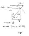
- the modulation vector M (t) rotating with the frequency ⁇is shown in a complex pointer representation.
- the modulation components 1 + S and Ddefine the instantaneous amplitude and phase ⁇ of the pointer compared to a reference pointer rotating with a constant amplitude and a constant frequency.
- the revolving reference pointerspecifies the reference phase via the in-phase signal I.
- the quadrature phase signal Qis perpendicular to this. From these two signals I, Q, the coordinate converter 3 determines the current length 1 + S and the current phase ⁇ of the pointer M (t).
- the pointer representationis independent of the rotation frequency ⁇ . This representation applies both to the high-frequency quadrature signal sq and to the quadrature components I, Q, the associated reference pointer of which rotates at the low rotation frequency ⁇ r .
- the implementation of the demodulator according to the inventioncan be done as a program in a processor, particularly in a monolithically integrated circuit, or as Circuit or in mixed form. It is irrelevant how the individual Functional units are realized in detail and whether the functional units are also different Serve purposes.
Landscapes
- Engineering & Computer Science (AREA)
- Multimedia (AREA)
- Physics & Mathematics (AREA)
- Acoustics & Sound (AREA)
- Signal Processing (AREA)
- Digital Transmission Methods That Use Modulated Carrier Waves (AREA)
- Stereo-Broadcasting Methods (AREA)
Description
Translated fromGermanDie Erfindung betrifft einen digitalen Demodulator für ein quadraturmoduliertes Signal,das mittels einer Amplituden- und Phasenmodulation ein Kombinationssignal überträgt.The invention relates to a digital demodulator for a quadrature-modulated signal,which transmits a combination signal by means of amplitude and phase modulation.
Quadraturmodulierte Signale werden gerne angewendet, wenn in einemÜbertragungskanal zusammengehörige Signale, die aber unabhängig voneinander seinsollen, zu übertragen sind. Eine derartige Anwendung ist die Übertragung vonStereosignalen nach dem C-QUAM-Standard, bei der ein Summensignal über dieAmplitudenmodulation und ein Differenzsignal sowie ein Pilotton über diePhasenmodulation des jeweiligen Trägers übertragen wird. Ein Beispiel für einenzugehörigen digitalen Demodulator ist in der Offenlegungschrift DE 43 40 012 A1beschrieben. Eine Quadratursignalquelle bildet aus dem empfangenenquadraturmodulierten Signal mittels eines Quadraturmischers ein Inphasensignal und einQuadraturphasensignal. Die Digitalisierung kann dabei vor oder nach demQuadraturmischer erfolgen. Mittels eines Koordinatenumsetzers, der insbesondere nachdem Cordic-Algorithmus arbeitet, wird aus dem digitalisierten Inphasensignal und demdigitalisierten Quadraturphasensignal ein Betragssignal und ein Phasensignal gebildet.Ein vom Phasensignal gesteuerter Regelkreis steuert die Oszillatorfrequenz desQuadraturmischers exakt auf den Wert der Trägerfrequenz, so daß das Inphasensignalund das Quadraturphasensignal in das Basisband transformiert werden. Eineverbleibende mittlere Phasenabweichung wird dadurch korrigiert, daß der Regelkreisauch in das Phasensignal eingreift und dort ein Korrektursignal addiert oder subtrahiert,das den zeitlichen Mittelwert des Phasensignals auf den Nullphasenwert zieht. EinDekodierer, der im wesentlichen eine bekannte Stereomatrix enthält, bildet aus demBetragssignal und dem Phasensignal das gesuchte Links- und Rechtssignal sowie dasPilotsignal bei 25 Hz.Quadrature modulated signals are often used when in oneSignals belonging to the transmission channel, but which are independent of one anotherare to be transferred. One such application is the transmission ofStereo signals according to the C-QUAM standard, in which a sum signal over theAmplitude modulation and a difference signal as well as a pilot tone over thePhase modulation of the respective carrier is transmitted. An example of oneassociated digital demodulator is published in DE 43 40 012 A1described. A quadrature signal source forms from the received onequadrature-modulated signal using a quadrature mixer, an in-phase signal and aQuadrature phase signal. Digitization can take place before or afterQuadrature mixer done. By means of a coordinate converter, in particular according toThe Cordic algorithm works from the digitized in-phase signal and thedigitized quadrature phase signal, a magnitude signal and a phase signal are formed.A control loop controlled by the phase signal controls the oscillator frequency of theQuadrature mixer exactly to the value of the carrier frequency, so that the in-phase signaland the quadrature phase signal are transformed into the baseband. Aremaining average phase deviation is corrected by the control loopalso intervenes in the phase signal and adds or subtracts a correction signal there,that pulls the temporal average of the phase signal to the zero phase value. OnDecoder, which essentially contains a known stereo matrix, forms from theAmount signal and the phase signal, the left and right signal as well as thePilot signal at 25 Hz.
Aufgabe der Erfindung ist es, einen verbesserten digitalen Demodulator für derartigequadraturmodulierte Signale anzugeben, der besser an die digitale Signalverarbeitung angepaßt ist und geringere Anforderungen an die Quadratursignalquelle stellt.The object of the invention is to provide an improved digital demodulator for suchQuadrature modulated signals indicate the better of digital signal processingis adapted and places less demands on the quadrature signal source.
Die Aufgabe wird durch die Erfindung entsprechend den Merkmalen des Anspruchs 1wie folgt gelöst:
- eine Quadratursignalquelle, die abhängig vom empfangenen quadraturmoduliertenSignal ein digitalisiertes Inphasensignal und ein digitalisiertesQuadraturphasensignal in tiefer Frequenzlage liefert,wobei die Bandbreite des tiefen Frequenzbereiches nicht größerist als ein Zehntel der Digitalisierungsfrequenz,
- ein Koordinatenumsetzer, der aus dem digitalisierten Inphasensignal und demdigitalisierten Quadraturphasensignal ein Betragssignal und ein erstes Phasensignalbildet,
- ein dem Koordinatenumsetzer nachgeschalteter erster Regelkreis, der die Steigungdes ersten Phasensignals im zeitlichen Mittel auf den Wert Null oder einen Restwertregelt und damit ein zweites Phasensignal bildet,
- ein dem Koordinatenumsetzer nachgeschalteter zweiter Regelkreis, der denzeitlichen Mittelwert des zweiten Phasensignals auf einen Phasenbezugswert,insbesondere eine Nullphasenlage, regelt und damit ein drittes Phasensignal bildet,und
- ein Dekodierer, der aus dem Betragssignal und dem dritten Phasensignal mindestenseine digitalisierte Komponente des Kombinationssignals bildet.
- a quadrature signal source which, depending on the received quadrature-modulated signal, supplies a digitized in-phase signal and a digitized quadrature-phase signal in the low frequency range, the bandwidth of the low frequency range being no greater than a tenth of the digitization frequency,
- a coordinate converter which forms a magnitude signal and a first phase signal from the digitized in-phase signal and the digitized quadrature phase signal,
- a first control circuit downstream of the coordinate converter, which regulates the slope of the first phase signal to the value zero or a residual value on average over time and thus forms a second phase signal,
- a second control circuit connected downstream of the coordinate converter, which regulates the time average of the second phase signal to a phase reference value, in particular a zero phase position, and thus forms a third phase signal, and
- a decoder which forms at least one digitized component of the combination signal from the magnitude signal and the third phase signal.
Der wesentliche Vorteil dieser Anordnung besteht darin, daß die Ausgangssignale derQuadratursignalquelle, das digitalsierte Inphasensignal und das digitalisierteQuadraturphasensignal nicht die exakte Basisbandlage aufweisen müssen, sondern nurin einem relativ tiefen Frequenzbereich liegen müssen. Die Bandbreite dieses tiefenFrequenzbereiches hängt von der Digitalisierungsfrequenz ab und soll dabei möglichstnicht größer sein als ein Zehntel der Digitalisierungsfrequenz. Diese günstigenRandbedingungen erlauben, daß ein digitaler Quadraturmischer auf einfachste Weisedurch digitale Umschalter zu realisieren ist, weil das quadraturmodulierte Digitalsignal lediglich mit den Werten +1, -1 und 0 zu multiplizieren ist. Bei einer exaktenTransformation des quadraturmodulierten Digitalsignals in das Basisband wäre eineexakte Frequenzanpassung des digitalen Mischungssignals erforderlich, was nur übereine sehr aufwendige Sinus- und/oder Cosinus-Tabelle mit zwei aufwendigen digitalenMultiplizierern zu realisieren wäre. Eine analoge Ausführung des Quadraturmischers mitnachfolgender Digitalisierung des Inphasen- und Quadraturphasensignals ist natürlichebenfalls möglich, wobei nach der Erfindung die Oszillatorfrequenz nicht nachgeregeltwerden muß und daher unkritisch gegenüber der Frequenzlage und Driftänderungen ist.Die Erfindung vermeidet somit eine phasenstarre Nachführung des Quadraturmischers,aufwendige Sinus- und/oder Cosinus-Tabellen und aufwendige Multiplizierer bei derQuadraturmischung.The main advantage of this arrangement is that the output signals of theQuadrature signal source, the digitized in-phase signal and the digitizedQuadrature phase signal do not have to have the exact baseband position, but onlymust be in a relatively low frequency range. The range of this deepFrequency range depends on the digitization frequency and should be as possiblenot be greater than a tenth of the digitization frequency. This cheapBoundary conditions allow that a digital quadrature mixer in the simplest waycan be realized by digital switchers because the quadrature modulated digital signalonly to be multiplied by the values +1, -1 and 0. With an exactTransforming the quadrature modulated digital signal into the baseband would be oneexact frequency adjustment of the digital mix signal required, which is only abouta very complex sine and / or cosine table with two complex digitalMultipliers would be realized. An analog version of the quadrature mixer withsubsequent digitization of the in-phase and quadrature-phase signal is naturallikewise possible, the oscillator frequency not being readjusted according to the inventionmust be and is therefore not critical to the frequency situation and drift changes.The invention thus avoids a phase-rigid tracking of the quadrature mixer,complex sine and / or cosine tables and complex multipliers in theQuadrature mixing.
Eine vorteilhafte Ansteuerung des ersten Regelkreises erfolgt über die Steigung des erstenPhasensignals, die sich aus der Differenzbildung zwischen mindestens zwei zeitlichbenachbarten Abtastwerten ergibt. Dies schließt selbstverständlich mit ein, daß weitereAbtastwerte zur Differenzbildung erfaßt werden können, wobei eine bessereMittelwertbildung erreicht wird und Störgrößen besser unterdrückt werden können.The first control loop is advantageously controlled via the slope of the firstPhase signal resulting from the difference between at least two in timeneighboring samples. Of course, this includes that othersSamples for difference formation can be acquired, with a better oneAveraging is achieved and disturbances can be suppressed better.
Für die Genauigkeit der Regelung ist es ferner zweckmäßig, wenn die Regelkreise einenIntegrator enthalten. Hierfür eignen sich insbesondere Akkumulatorschleifen mitgenügender Stellenkapazität, damit im Normalbetrieb kein Überlauf stattfindet.For the accuracy of the control, it is also expedient if the control loops have oneIntegrator included. Accumulator loops are particularly suitable for thissufficient job capacity so that there is no overflow in normal operation.
Von Vorteil ist, wenn das Stellsignal des ersten und/oder zweiten Regelkreises derartausgebildet ist, daß es als additives oder subtraktives Korrektursignal über eineAddierschaltung mit dem jeweiligen Phasensignal kombiniert werden kann. Beigeeigneter Ausführung der beiden Regelkreise lassen sich die beiden Stellsignale additivkombinieren, so daß nur ein einziger Addierer zur Korrektur im Phasensignalpfaderforderlich ist. In gleicher Weise kann der Integrator für den ersten und zweitenRegelkreis gemeinsam ausgebildet sein, indem die beiden Stellsignale dem Addierer imAkkumulatorkreis zugeführt sind. Dessen Ausgang liefert dann das gemeinsameStellsignal.It is advantageous if the control signal of the first and / or second control loop is of this typeis designed that it as an additive or subtractive correction signal via aAdding circuit can be combined with the respective phase signal. atIf the two control loops are designed appropriately, the two control signals can be addedcombine so that only a single adder for correction in the phase signal pathis required. In the same way, the integrator for the first and secondControl loop can be formed together by the two control signals in the adderAccumulator circuit are supplied. Its output then provides the common oneActuating signal.
Für die jeweilige Übertragungsnorm kann es erforderlich sein, daß das dritte Phasensignal vor dem Dekodierer mittels einer Modifizierungseinrichtung zu modifizierenist. Die Modifizierungseinrichtung entspricht einer vorgegebenen Signalkennlinie, die inverszur Signalkennlinie auf der Senderseite ist. Die Modifizierungseinrichtung kann dabei einenichtlineare Kennlinie aufweisen, z.B. ist bei dem C-QUAM-Standard als Kennlinie aufder Empfängerseite ein Tangensverlauf vorgeschrieben. Der Tangensverlauf kann dabeidurch eine Speichertabelle definiert sein oder durch eine Polynomannäherung wie in derbereits genannten DE 43 40 012.It may be necessary for the respective transmission standard that the thirdModify phase signal before the decoder by means of a modification deviceis. The modification device corresponds to a predetermined signal characteristic, the inverseto the signal characteristic on the transmitter side. The modification device can be ahave nonlinear characteristics, e.g. is on the C-QUAM standard as a characteristica tangent curve is prescribed for the receiver side. The tangent course canbe defined by a memory table or by a polynomial approximation as in theDE 43 40 012 already mentioned.
Die Erfindung und vorteilhafte Ausgestaltungen werden nun anhand der Zeichnung mitmehreren Figuren näher erläutert:
In der schematischen Darstellung von Fig. 1 empfängt eine Eingangsstufe 1 einqudraturmoduliertes Signal sq von einer Antenne, einem Kabel oder einer sonstigenEinrichtung. Eine Quadratursignalquelle 2 mit angeschlossenem Oszillator 2.1, der alsMischungssignal sx ein digitales Signal mit einer vorgegebenen Frequenz fx abgibt, bildetaus dem quadraturmodulierten Signal sq ein Inphasensignal I und einQuadraturphasensignal Q, wobei beide Signale I und Q digitalisiert sind. DieDigitalisierung kann dabei in der Quadratursignalquelle 2 oder bereits in derEingangssstufe 1 erfolgen.In the schematic representation of FIG. 1, an
Zum Verständnis für das C-QUAM-Stereo-Übertragungsverfahren werden im folgenden,einige kurze Erläuterungen eingeschoben, vgl. hierzu Fig. 4. Die Abkürzung C-QUAMsteht für "Compatibel - Quadratur Amplitude Modulation", einem AM-Stereoübertragungsverfahren,das von Motorola entwickelt wurde und zur Zeitinsbesondere in USA und Australien verwendet wird. Für die Stereoübertragung wird aus der Links- und Rechtsinformation L bzw. R, wie bei nahezu allen Stereo-Standards,zuächst in ein Summen- und ein Differenzsignal S bzw. D gebildet:
Das modulierte Signal erhält man aus dem Realteil (=Re) und Imaginärteil eineskomplexen Zeigers M(t), der sich entsprechend der Trägerfrequenz f mit derRotationsfrequenz ω dreht. Der Betrag dieses Zeigers soll dabei immer den Wert 1+Sannehmen, wobei der Wert 1 den Träger mit konstant angenommener Größerepräsentiert. Die Größe des Differenzsignals D wirkt sich ausschließlich auf diePhasenlage des Zeigers M(t) aus. Der Phasenwinkel ϕ des Modulationsvektors M(t)ergibt sich zu:
Das auf die Trägeramplitude normierte C-QUAM-Signal kann somit durch folgendenAusdruck beschrieben werden:
Auf das Differenzsignal D wird ferner ein Pilotton P mit einer Frequenz von 25 Hz bei5 % Aussteuerung moduliert, der eine Stereoerkennung und damit eine automatischeStereoumschaltung ermöglicht.A pilot tone P with a frequency of 25 Hz is also applied to the difference signal D.5% modulation modulated, the stereo detection and thus an automaticStereo switching enabled.
In Fig. 1 schließt sich an die Quadratursignalquelle 2 ein Koordinatenumsetzer 3 an, deraus dem Inphasensignal I und dem Quadraturphasensignal Q ein Betragssginal b und einerstes Phasensignal p1 bildet. Der Koordinatenumsetzer 3 führt eine Umsetzung vonkarthesischen Koordinaten in Polarkoordinaten aus. Für diese Umsetzung eignet sichinsbesondere der bekannte Cordic-Algorithmus, der die gesuchten Werte über eineiterative Näherung mit beliebiger Genauigkeit bestimmt.In Fig. 1, the
Wie eingangs erwähnt, ist es nicht erforderlich, daß die Quadraturmischung direkt in dasBasisband erfolgt. Wenn das Inphasensignal I und das Quadraturphasensignal Q mit einer Frequenz von 19 kHz abgetastet werden, dann reicht es für die Demodulation nachder Erfindung aus, wenn die restliche Rotationsfrequenz ωr des komplexen Zeigers M(t)kleiner als 2 kHz bleibt.As mentioned at the beginning, it is not necessary for the quadrature mixing to take place directly in the baseband. If the in-phase signal I and the quadrature phase signal Q are sampled at a frequency of 19 kHz, then it is sufficient for the demodulation according to the invention if the remaining rotational frequency ωr of the complex pointer M (t) remains less than 2 kHz.
Die Differenz aus der Mischungsfrequenz fx und der Trägerfrequenz f ergibt eineRestfrequenz fr und damit eine verbleibende Rotationsfrequenz ωr des komplexen ZeigersM(t). Sie bewirkt, daß das erste Phasensignal p1 nicht konstant ist sondern im zeitlichenMittel konstant zu- oder abnimmt, vgl. auch Fig. 2. Dies entspricht einer konstantenVersatzfrequenz ωr die mittels eines ersten Regelkreises 4 auf den Wert Null gebrachtwird, indem die mittlere Steigung mt des ersten Phasensignals p1 durch ein erstesStellsignal c1 mit einer gleichgroßen negativen Steigung kompensiert wird. DasStellsignal c1 wird mittels eines ersten Addierers 5 dem ersten Phasensignal p1hinzugefügt und bildet damit ein zweites Phasensignal p2, vgl. auch Fig. 3. In Fig. 1 wirddie Steigung durch einen Differenzbildner 6 aus zwei aufeinanderfolgenden Abtastwertengebildet, die dann mittels einer ersten Filtereinrichtung 7 gewichtet und/oder gemitteltwerden. Der Ausgang der ersten Filtereinrichtung 7 wird mittels eines Integrators 8integriert, dessen Ausgang das erste Stellsignal c1 an den ersten Addierer 5 liefert. DerDifferenzbildner 6 besteht aus einem ersten Verzögerer 6.1 und einem Subtrahierer 6.2.Der Integrator 8 besteht aus einer Akkumulatorschleife mit einem zweiten Addierer 8.1und einem zweiten Verzögerer 8.2. Die Ausgangssignale der beiden Regelschleifen 4, 9werden dem zweiten Addierer 8.1 als invertierte Signale zugeführt, damit dieRegelrichtung beim ersten Addierer 5 stimmt.The difference between the mixing frequency fx and the carrier frequency f results in a residual frequency fr and thus a remaining rotational frequency ωr of the complex pointer M (t). It has the effect that the first phase signal p1 is not constant but increases or decreases constantly over time, cf. also Fig. 2. This corresponds to a constant offset frequency ωr which is brought to the value zero by means of a
Die Kompensation der mittleren Steigung mp bewirkt aber noch nicht, daß das zweitePhasensignal p2 im zeitlichen Mittel exakt auf den Phasenbezugswert zu liegen kommt.Der zeitliche Mittelwert tm des zweiten Phasensignals p2 ist in Fig. 3 als leichtansteigende Gerade unterhalb der Nullphasenbezugsachse dargestellt. Mittels eineszweiten Regelkreises 9 wird der zeitliche Mittelwert tm des zweiten Phasensignals p2exakt auf die Nullphasenbezugsachse gebracht. Dies wird mittels einer zweitenFiltereinrichtung 10 und dem Integrator 8 erreicht, indem das Ausgangssignal des erstenAddierers 5 direkt oder über eine Modifizierungseinrichtung 11 dem Eingang der zweitenFiltereinrichtung 10 zugeführt wird, an deren Ausgang ein weiterer Eingang desIntegrators 8 liegt. Als Ergebnis bildet der zweite Regelkreis 9 ein zweites Stellsignal c2, das mittels des ersten Addierers 5 additiv/subtraktiv dem erstenPhasensignal p1 und einem ersten Stellsignal c1 hinzugefügt wird und damit ein drittes Phasensignal p3 bildet, dasbezüglich seiner Steigung und Phase im zeitlichen Mittel richtig liegt. Das zweitePhasensignal p2 liefert mit seinem Mittelwert mp2 das Eingangssignal des zweitenRegelkreises. Die momentanen Abweichungen des dritten Phasensignals p3 von derNullphasenbezugslage entsprechen somit nur noch dem gesuchten Differenzsignal D unddem Pilotsignal P. Mittels eines Dekodierers 12 werden aus dem Betragssignal b unddem dritten Phasensignal p3 die gesuchten Komponenten L, R, P des Stereo-Kombinationssignalsgebildet. Entsprechend dem Übertragungsstandard wird in derRegel zuvor das dritte Phasensignal p3 mittels der Modifizierungseinrichtung 11 modifiziert,indem beispielsweise der zugehörige Tangenswert bestimmt wird. Da im Betragssignalb die Trägeramplitude enthalten ist, wird für die Stereo-Matrix im Dekodierer 12 dasdritte Phasensignal p3 bzw. das modifizierte Phasensignal p3' auf die Trägeramplitudenormiert. Dies erfolgt mittels eines Multiplizierers 13, dessen erster Eingang mit demBetragssignal b und dessen zweiter Eingang mit dem dritten Phasensignal p3 bzw. p3'gespeist ist.However, the compensation of the mean slope mp does not cause the secondPhase signal p2 comes to lie exactly on the phase reference value on average over time.The time average tm of the second phase signal p2 is easy in FIG. 3rising straight line shown below the zero phase reference axis. By means of a
Es wird darauf hingewiesen, daß in Fig. 1 das zweite und dritte Phasensignal p2, p3identisch sind, weil der Ausgang des ersten und zweiten Regelkreises 4, 9 durch dengemeinsamen Addierer 5 gebildet wird. Die Funktionsweise des Demodulators wirddurch die getrennte Betrachtung von p2, p3 verständlicher.It is pointed out that in FIG. 1 the second and third phase signals p2, p3are identical because the output of the first and
In Fig. 2 ist schematisch der zeitliche Verlauf des ersten Phasensignals p1 dargestellt. Derrestlichen Rotationsfrequenz ωr des komplexen Zeigers M(t) entspricht eine stetigeZunahme mp der mittleren Phase mp1, die durch eine sägezahnförmige, durchgezogeneLinie dargestellt ist. Das erste Phasensignal p1 wird vorzugsweise alsZweierkomplement-Zahlenwert dargestellt, dessen untere bzw. obere Wertegrenze demPhasenwinkel -π bzw. +π entspricht. Die stetig zunehmende Phase mp1 springt somitgleichsam von dem Phasenwert +π auf den Phasenwert -π zurück. Die Ankopplung desjeweiligen Phasenwertes an die Zweierkomplement-Zahlendarstellung hat den großenVorteil, daß Phasendifferenzwerte richtig wiedergegeben werden, auch wenn die Phasezwischenzeitlich übergelaufen ist. Der gestrichelte Bereich um die mittlere Phase mp1gibt den Bereich an, in dem sich das erste Phasensignal p1 durch die Modulation mit dem Differenzsignal D und dem Pilotsignal P aufhalten kann.2 schematically shows the time profile of the first phase signal p1. The remaining rotation frequency ωr of the complex pointer M (t) corresponds to a steady increase mp in the middle phase mp1, which is represented by a sawtooth-shaped, solid line. The first phase signal p1 is preferably represented as a two's complement number whose lower or upper value limit corresponds to the phase angle -π or + π. The steadily increasing phase mp1 thus jumps back from the phase value + π to the phase value -π. The coupling of the respective phase value to the two's complement number representation has the great advantage that phase difference values are reproduced correctly, even if the phase has meanwhile overflowed. The dashed area around the middle phase mp1 indicates the area in which the first phase signal p1 can be due to the modulation with the difference signal D and the pilot signal P.
In Fig. 3 ist schematisch der zeitliche Verlauf des zweiten Phasensignals p2 dargestellt,das durch eine Phasenkorrektur mittels des ersten Regelkreises 4 erhalten wird. Diemittlere Phase mp2 hat hierbei allenfalls noch eine ganz geringfügige Steigung tm. Diemittlere Phase mp2 liegt jedoch nicht wie erforderlich auf der Nullphasen-Bezugsachse- allenfalls zufällig. Die Korrektur der Nullphasenlage erfolgt durch den zweitenRegelkreis 9, der auch die geringfügige restliche Steigung tm unterdrückt. Diemomentane Phase des zweiten Phasensignals p2 liegt dabei in dem gestricheltdargestellten Phasenbereich um die mittlere Phase mp2.3 schematically shows the time profile of the second phase signal p2,which is obtained by a phase correction by means of the
In Fig. 4 wird wie bereits erläuert in einer komplexen Zeigerdarstellung der mit derFrequenz ω rotierende Modulationsvektor M(t) dargestellt. Die Modulationskomponenten1+S und D definieren dabei die momentane Amplitude und Phase ϕ des Zeigersgegenüber einem mit konstanter Amplitude und mit konstanter Frequenz umlaufendenBezugszeiger. Beim hochfrequent übertragenen Quadratursignal sq ist dies derzugehörige Träger. Der umlaufende Bezugszeiger gibt über das Inphasensignal I dieBezugsphase vor. Senkrecht dazu steht das Quadraturphasensignal Q. Aus diesen beidenSignalen I,Q bestimmt der Koordinatenumsetzer 3 die momentane Länge 1+S undmomentane Phase ϕ des Zeigers M(t). Die Zeigerdarstellung ist unabhängig von derRotationsfrequenz ω. So gilt diese Darstellung sowohl für das hochfrequent übertrageneQuadratursignal sq als auch für die Quadraturkomponenten I,Q, deren zugehörigerBezugszeiger mit der niedrigen Rotationsfrequenz ωr umläuft.As already explained in FIG. 4, the modulation vector M (t) rotating with the frequency ω is shown in a complex pointer representation. The
Die Realisierung des Demodulators nach der Erfindung kann als Programmablauf ineinem Prozessor, insbesondere in einer monolithisch integrierten Schaltung, oder alsSchaltung oder in gemischter Form erfolgen. Es ist dabei unerheblich, wie die einzelnenFuntionseinheiten im Detail realisiert sind und ob die Funktionseinheiten auch anderenZwecken dienen.The implementation of the demodulator according to the invention can be done as a program ina processor, particularly in a monolithically integrated circuit, or asCircuit or in mixed form. It is irrelevant how the individualFunctional units are realized in detail and whether the functional units are also differentServe purposes.
Claims (7)
- A digital demodulator for a quadrature-modulatedsignal (sq) which transmits a combination signal byamplitude and phase modulation, said digital demodulatorcomprising:a quadrature-signal source (2) which, in response tothe received quadrature-modulated signal (sq),provides a digitized in-phase component (I) and adigitized quadrature component (Q) at a low frequency,the width of the low-frequency range being not greaterthan one tenth of the digitization frequency;a resolver (3) which converts the digitized in-phasecomponent (I) and the digitized quadrature component(Q) into a magnitude signal (b) and a first phasesignal (p1);a first feedback control loop (4) following theresolver (3), which, on a time average, maintains theslope of the first phase signal (p1) at the zero valueor a residual value, thus forming a second phasesignal (p2);a second feedback control loop (9) following theresolver (3), which maintains the time average of thesecond phase signal (p2) at a phase reference value,particularly at a zero phase value, thus forming athird phase signal (p3); anda decoder (12) which produces at least one digitizedcomponent (R, L, P) of the combination signal from themagnitude signal (b) and the third phase signal (p3).
- A demodulator as set forth in claim 1,characterizedin that the slope (mp) of the first phase signal (p1) isformed from the difference between at least twotemporally adjacent sample values.
- A demodulator as set forth in claim 1 or 2,characterized in that the first feedback control loop (4)and/or the second feedback control loop (9) comprise anintegrator (8).
- A demodulator as set forth in any one of claims 1 to3,characterized in that the first feedback control loop(4) and the second feedback control loop (9) form a firstcorrective signal (c1) and a second corrective signal(c2), respectively, with which the first phase signal(p1) and the second phase;signal (p2), respectively, areadditively/subtractively changed in value.
- A demodulator as set forth in claim 3,characterizedin that the integrator (8) is common to the first andsecond feedback control loops (4, 9).
- A demodulator as set forth in any one of claims 1 to5,characterized in that the third phase signal (p3) isapplied to the decoder (12) and/or to the second feedbackcontrol loop (9) through a modification device (11).
- A demodulator as set forth in claim 6,characterizedin that the modification device (11) comprises a tangent-formingdevice.
Priority Applications (3)
| Application Number | Priority Date | Filing Date | Title |
|---|---|---|---|
| EP96101105AEP0786921B1 (en) | 1996-01-26 | 1996-01-26 | Digital demodulator |
| DE59609450TDE59609450D1 (en) | 1996-01-26 | 1996-01-26 | Digital demodulator |
| US08/792,924US5767739A (en) | 1996-01-26 | 1997-01-21 | Digital demodulator for quadrature amplitude and phase modulated signals |
Applications Claiming Priority (1)
| Application Number | Priority Date | Filing Date | Title |
|---|---|---|---|
| EP96101105AEP0786921B1 (en) | 1996-01-26 | 1996-01-26 | Digital demodulator |
Publications (2)
| Publication Number | Publication Date |
|---|---|
| EP0786921A1 EP0786921A1 (en) | 1997-07-30 |
| EP0786921B1true EP0786921B1 (en) | 2002-07-17 |
Family
ID=8222441
Family Applications (1)
| Application Number | Title | Priority Date | Filing Date |
|---|---|---|---|
| EP96101105AExpired - LifetimeEP0786921B1 (en) | 1996-01-26 | 1996-01-26 | Digital demodulator |
Country Status (3)
| Country | Link |
|---|---|
| US (1) | US5767739A (en) |
| EP (1) | EP0786921B1 (en) |
| DE (1) | DE59609450D1 (en) |
Families Citing this family (7)
| Publication number | Priority date | Publication date | Assignee | Title |
|---|---|---|---|---|
| DE4434451A1 (en)* | 1994-09-27 | 1996-03-28 | Blaupunkt Werke Gmbh | Amplitude demodulator |
| KR100441196B1 (en)* | 2002-01-14 | 2004-07-21 | 기가텔레콤 (주) | Apparatus for continuous phase quadrature amplitude modulation and demodulation |
| BR0304231A (en) | 2002-04-10 | 2004-07-27 | Koninkl Philips Electronics Nv | Methods for encoding a multi-channel signal, method and arrangement for decoding multi-channel signal information, data signal including multi-channel signal information, computer readable medium, and device for communicating a multi-channel signal. |
| DE102004020300B3 (en)* | 2004-04-26 | 2005-09-22 | Micronas Gmbh | Pulsed signal method for determining a pulsed signal's scan-time point operates with a circuit structure for determining symbols from a digitized signal |
| US10509295B2 (en)* | 2017-03-15 | 2019-12-17 | Elenion Technologies, Llc | Bias control of optical modulators |
| US10942377B2 (en)* | 2018-10-08 | 2021-03-09 | Cisco Technology, Inc. | High swing AC-coupled Mach-Zehnder interferometer (MZI) driver |
| CN111510406B (en)* | 2020-06-03 | 2024-05-17 | 上海创远仪器技术股份有限公司 | Circuit and method for implementing real-time predistortion calibration of broadband IQ modulation |
Family Cites Families (5)
| Publication number | Priority date | Publication date | Assignee | Title |
|---|---|---|---|---|
| JPS6047513A (en)* | 1983-08-26 | 1985-03-14 | Nec Corp | Frequency shift absorbing circuit |
| DE3889326D1 (en)* | 1988-05-27 | 1994-06-01 | Itt Ind Gmbh Deutsche | Correction circuit for a digital quadrature signal pair. |
| US5249204A (en)* | 1991-08-12 | 1993-09-28 | Motorola, Inc. | Circuit and method for phase error correction in a digital receiver |
| DE4340012B4 (en) | 1993-11-24 | 2004-04-22 | Blaupunkt-Werke Gmbh | demodulator |
| US5497400A (en)* | 1993-12-06 | 1996-03-05 | Motorola, Inc. | Decision feedback demodulator with phase and frequency estimation |
- 1996
- 1996-01-26EPEP96101105Apatent/EP0786921B1/ennot_activeExpired - Lifetime
- 1996-01-26DEDE59609450Tpatent/DE59609450D1/ennot_activeExpired - Fee Related
- 1997
- 1997-01-21USUS08/792,924patent/US5767739A/ennot_activeExpired - Lifetime
Also Published As
| Publication number | Publication date |
|---|---|
| DE59609450D1 (en) | 2002-08-22 |
| EP0786921A1 (en) | 1997-07-30 |
| US5767739A (en) | 1998-06-16 |
Similar Documents
| Publication | Publication Date | Title |
|---|---|---|
| DE68926583T2 (en) | Interference suppression circuit | |
| DE69318818T2 (en) | DEVICE FOR COMPENSATING THE PHASE ROTATION IN A POWER AMPLIFIER | |
| DE2309167C2 (en) | Method and circuit arrangement for correcting an electrical transmission signal corrupted by phase tremors | |
| EP0895386B1 (en) | Carrier control circuit for a receiver of digital transmitted signals | |
| DE69629855T2 (en) | amplifier device | |
| DE2646255A1 (en) | DIGITAL DETECTOR SYSTEM FOR DIFFERENTIAL PHASE SHIFT TOGGLE SIGNALS | |
| EP0084876A2 (en) | Demodulator arrangement for signals which are frequency-modulated on a carrier wave | |
| DE2902952A1 (en) | DIRECTLY MIXING RECEIVING SYSTEM | |
| DE2257275C3 (en) | Circuit arrangement for automatic equalization | |
| DE69332216T2 (en) | Carrier wave recovery processor for a QAM television signal | |
| DE964250C (en) | Receiver for vestigial sideband signals | |
| DE2656924C3 (en) | Phase discriminator in a receiver of a data transmission system | |
| EP0786921B1 (en) | Digital demodulator | |
| DE69729329T2 (en) | APPARATUS AND METHOD FOR ESTIMATING THE PHASE | |
| WO2005125143A1 (en) | Method and device for the simultaneous compensation of signal errors in iq-modulators | |
| EP0579100A1 (en) | Method and apparatus for baseband phase correction in a PSK receiver | |
| DE102007028066B3 (en) | Method and apparatus for generating a transmission signal | |
| DE69818075T2 (en) | SIGNAL PROCESSING SYSTEM | |
| DE2842111A1 (en) | AM STEREO RECEIVER | |
| DE1591408C2 (en) | Device for receiving several input signals of the same frequency | |
| DE69927957T2 (en) | Demodulator with rotation means for frequency offset correction | |
| DE4340012B4 (en) | demodulator | |
| EP0602394B1 (en) | Method and device for the correction of phase and amplitude errors for direct conversion receiving devices | |
| DE2715741A1 (en) | STEREO TRANSMISSION DEVICE | |
| DE2654276A1 (en) | PHASE-SYNCHRONIZING CIRCUIT ARRANGEMENT |
Legal Events
| Date | Code | Title | Description |
|---|---|---|---|
| PUAI | Public reference made under article 153(3) epc to a published international application that has entered the european phase | Free format text:ORIGINAL CODE: 0009012 | |
| AK | Designated contracting states | Kind code of ref document:A1 Designated state(s):DE FR GB IT NL | |
| RAP1 | Party data changed (applicant data changed or rights of an application transferred) | Owner name:MICRONAS INTERMETALL GMBH | |
| 17P | Request for examination filed | Effective date:19980130 | |
| RAP1 | Party data changed (applicant data changed or rights of an application transferred) | Owner name:MICRONAS GMBH | |
| GRAG | Despatch of communication of intention to grant | Free format text:ORIGINAL CODE: EPIDOS AGRA | |
| 17Q | First examination report despatched | Effective date:20010912 | |
| GRAG | Despatch of communication of intention to grant | Free format text:ORIGINAL CODE: EPIDOS AGRA | |
| GRAG | Despatch of communication of intention to grant | Free format text:ORIGINAL CODE: EPIDOS AGRA | |
| GRAH | Despatch of communication of intention to grant a patent | Free format text:ORIGINAL CODE: EPIDOS IGRA | |
| GRAH | Despatch of communication of intention to grant a patent | Free format text:ORIGINAL CODE: EPIDOS IGRA | |
| GRAA | (expected) grant | Free format text:ORIGINAL CODE: 0009210 | |
| AK | Designated contracting states | Kind code of ref document:B1 Designated state(s):DE FR GB IT NL | |
| REG | Reference to a national code | Ref country code:GB Ref legal event code:FG4D Free format text:NOT ENGLISH | |
| GBT | Gb: translation of ep patent filed (gb section 77(6)(a)/1977) | Effective date:20020718 | |
| REF | Corresponds to: | Ref document number:59609450 Country of ref document:DE Date of ref document:20020822 | |
| ET | Fr: translation filed | ||
| PLBE | No opposition filed within time limit | Free format text:ORIGINAL CODE: 0009261 | |
| STAA | Information on the status of an ep patent application or granted ep patent | Free format text:STATUS: NO OPPOSITION FILED WITHIN TIME LIMIT | |
| 26N | No opposition filed | Effective date:20030422 | |
| PGFP | Annual fee paid to national office [announced via postgrant information from national office to epo] | Ref country code:NL Payment date:20070124 Year of fee payment:12 | |
| PGFP | Annual fee paid to national office [announced via postgrant information from national office to epo] | Ref country code:GB Payment date:20070125 Year of fee payment:12 | |
| PGFP | Annual fee paid to national office [announced via postgrant information from national office to epo] | Ref country code:DE Payment date:20070228 Year of fee payment:12 | |
| PGFP | Annual fee paid to national office [announced via postgrant information from national office to epo] | Ref country code:IT Payment date:20070521 Year of fee payment:12 | |
| PGFP | Annual fee paid to national office [announced via postgrant information from national office to epo] | Ref country code:FR Payment date:20070117 Year of fee payment:12 | |
| GBPC | Gb: european patent ceased through non-payment of renewal fee | Effective date:20080126 | |
| NLV4 | Nl: lapsed or anulled due to non-payment of the annual fee | Effective date:20080801 | |
| PG25 | Lapsed in a contracting state [announced via postgrant information from national office to epo] | Ref country code:NL Free format text:LAPSE BECAUSE OF NON-PAYMENT OF DUE FEES Effective date:20080801 Ref country code:DE Free format text:LAPSE BECAUSE OF NON-PAYMENT OF DUE FEES Effective date:20080801 | |
| REG | Reference to a national code | Ref country code:FR Ref legal event code:ST Effective date:20081029 | |
| PG25 | Lapsed in a contracting state [announced via postgrant information from national office to epo] | Ref country code:GB Free format text:LAPSE BECAUSE OF NON-PAYMENT OF DUE FEES Effective date:20080126 | |
| PG25 | Lapsed in a contracting state [announced via postgrant information from national office to epo] | Ref country code:FR Free format text:LAPSE BECAUSE OF NON-PAYMENT OF DUE FEES Effective date:20080131 | |
| PG25 | Lapsed in a contracting state [announced via postgrant information from national office to epo] | Ref country code:IT Free format text:LAPSE BECAUSE OF NON-PAYMENT OF DUE FEES Effective date:20080126 |