EP0786871B1 - Programmable logic array integrated circuits - Google Patents
Programmable logic array integrated circuitsDownload PDFInfo
- Publication number
- EP0786871B1 EP0786871B1EP97106242AEP97106242AEP0786871B1EP 0786871 B1EP0786871 B1EP 0786871B1EP 97106242 AEP97106242 AEP 97106242AEP 97106242 AEP97106242 AEP 97106242AEP 0786871 B1EP0786871 B1EP 0786871B1
- Authority
- EP
- European Patent Office
- Prior art keywords
- conductors
- programmable logic
- multiplexer
- programmable
- elements
- Prior art date
- Legal status (The legal status is an assumption and is not a legal conclusion. Google has not performed a legal analysis and makes no representation as to the accuracy of the status listed.)
- Expired - Lifetime
Links
Images


Classifications
- H—ELECTRICITY
- H03—ELECTRONIC CIRCUITRY
- H03K—PULSE TECHNIQUE
- H03K19/00—Logic circuits, i.e. having at least two inputs acting on one output; Inverting circuits
- H03K19/02—Logic circuits, i.e. having at least two inputs acting on one output; Inverting circuits using specified components
- H03K19/173—Logic circuits, i.e. having at least two inputs acting on one output; Inverting circuits using specified components using elementary logic circuits as components
- H03K19/1733—Controllable logic circuits
- H03K19/1737—Controllable logic circuits using multiplexers
- H—ELECTRICITY
- H03—ELECTRONIC CIRCUITRY
- H03K—PULSE TECHNIQUE
- H03K19/00—Logic circuits, i.e. having at least two inputs acting on one output; Inverting circuits
- H03K19/02—Logic circuits, i.e. having at least two inputs acting on one output; Inverting circuits using specified components
- H03K19/173—Logic circuits, i.e. having at least two inputs acting on one output; Inverting circuits using specified components using elementary logic circuits as components
- H03K19/177—Logic circuits, i.e. having at least two inputs acting on one output; Inverting circuits using specified components using elementary logic circuits as components arranged in matrix form
- H03K19/17704—Logic circuits, i.e. having at least two inputs acting on one output; Inverting circuits using specified components using elementary logic circuits as components arranged in matrix form the logic functions being realised by the interconnection of rows and columns
- H—ELECTRICITY
- H03—ELECTRONIC CIRCUITRY
- H03K—PULSE TECHNIQUE
- H03K19/00—Logic circuits, i.e. having at least two inputs acting on one output; Inverting circuits
- H03K19/02—Logic circuits, i.e. having at least two inputs acting on one output; Inverting circuits using specified components
- H03K19/173—Logic circuits, i.e. having at least two inputs acting on one output; Inverting circuits using specified components using elementary logic circuits as components
- H03K19/177—Logic circuits, i.e. having at least two inputs acting on one output; Inverting circuits using specified components using elementary logic circuits as components arranged in matrix form
- H03K19/17724—Structural details of logic blocks
- H03K19/17728—Reconfigurable logic blocks, e.g. lookup tables
- H—ELECTRICITY
- H03—ELECTRONIC CIRCUITRY
- H03K—PULSE TECHNIQUE
- H03K19/00—Logic circuits, i.e. having at least two inputs acting on one output; Inverting circuits
- H03K19/02—Logic circuits, i.e. having at least two inputs acting on one output; Inverting circuits using specified components
- H03K19/173—Logic circuits, i.e. having at least two inputs acting on one output; Inverting circuits using specified components using elementary logic circuits as components
- H03K19/177—Logic circuits, i.e. having at least two inputs acting on one output; Inverting circuits using specified components using elementary logic circuits as components arranged in matrix form
- H03K19/17736—Structural details of routing resources
Definitions
- This inventionrelates to programmable logic array integrated circuits, and more particularly to programmable logic array integrated circuits with improved arrangements of the programmable logic elements and improved interconnections between those elements.
- Programmable logic arraysare known in which substantial numbers of relatively elementary individual programmable logic elements are provided in a two-dimensional array.
- the arrayalso includes a grid of intersecting signal conductors for conducting logic signals to, from, and between the programmable logic elements.
- Such programmable logic arraysare shown, for example, in U.S. patents 4,642,487, 4,706,216, 4,758,985, and 4,870,302, and in EP-A-0 426 283.
- Described hereinare programmable logic array integrated circuits in which signal conductors are interconnected not by relatively large and complex programmable interconnections, but by relatively small and simple fixed interconnections to multiplexers which can then be programmable to effect the desired interconnections.
- a simple non-programmable transverse connectionis made to each of those other conductors, and the transverse connections are applied in parallel to a multiplexer.
- the multiplexercan then be. programmed to select one of its inputs as its output.
- the output of the multiplexercan be an input to a programmable logic element, an output from the integrated circuit, or a lead which is programmably connectable to one or more of several other conductors in the device.
- Another interconnection technique described hereinis the grouping of the programmable logic elements into a plurality of mutually exclusive groups, each group having associated with it one or more conductors which can only be used to interconnect the elements in that group.
- Grouping the programmable logic elements in mutually exclusive (i.e., non-overlapping) groupshelps to simplify the task of programming the device by breaking the device down into several discrete parts, each of which is smaller and more easily managed than the whole device.
- Providing signal conductors which serve only to interconnect the programmable logic elements in each groupavoids tying up much longer conductors just to make short interconnections between adjacent programmable logic elements. This helps to reduce the required number of long conductors.
- each programmable logic elementmay be augmented with a programmable output stage which can be used either to feed the output of that programmable logic element to conductors which go beyond the associated group or to the interconnect conductors of the associated group.
- Multiplexerscan also be used in combination with programmable signal conductor interconnections to allow certain of the conductors to be laid down more densely, to reduce the size of the interconnection array, and to reduce the capacitive loading on each output conductor of the array.
- programmable signal conductor interconnectionsinstead of one output conductor crossing a large number of parallel input conductors with a programmable interconnection at each intersection of the output conductor with the input conductors (which tends to force relatively wide spacing of the input conductors because of the relatively large size of the programmable interconnections), two substantially parallel output conductors feeding a programmably controlled output multiplexer are used.
- Each of these output conductorshas a programmable interconnection only with every other one of the input conductors, and the input conductors which are thus connectable to one of the output conductors are interdigitated with the input conductors which are connectable to the other one of the output conductors.
- a single programmable elementcan be used to control two interconnections, one of which is on one output conductor, and the other of which is on the other output conductor.
- the output multiplexerthen makes the final selection of the desired output signal. Reducing the number of programmable elements in this way may be especially beneficial when the programmable elements are relatively large (e.g., as compared to the signal conductor interconnection elements they control). Indeed, it may be desirable to use more than two output signal conductors feeding the programmably controlled output multiplexer and to have each programmable element control one interconnection element on each of the more than two output conductors to still further reduce the required number of programmable elements.
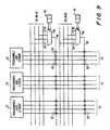
- FIG. 1is a simplified block diagram of a programmable logic array integrated circuit.
- FIG. 2is a more detailed block diagram of a representative portion of the circuit of FIG. 1.
- FIG. 3is a still more detailed schematic block diagram of a representative portion of FIG. 2.
- FIG. 4is a schematic block diagram showing a portion of FIG. 3 in still more detail.
- FIGS. 5-9are schematic diagrams showing alternative ways of making certain interconnections in circuits of the type shown in other drawings.
- an illustrative programmable logic array integrated circuit 10includes a two-dimensional array of groups 12 of programmable logic elements.
- the representative portion of FIG. 1 which is surrounded by broken line 14 and which includes a typical group 12is shown in more detail in FIG. 2.
- the structure shown in FIG. 2is sometimes referred to herein as a logic array block or LAB.
- integrated circuit 10(FIG. 1) is an eight by eight two-dimensional array of 64 LABs 14.
- each LAB 14includes 16 programmable logic elements or macrocells 20, a representative one of which is shown in more detail in FIG. 3.
- each programmable logic element 20includes a D-type flip-flop and four-input look-up table element 22 (shown in more detail in FIG. 4) and tri-state driver logic 24.
- each element 22includes a four-input look-up table 30 which is programmable to produce a desired binary output signal value for each of the 16 possible combinations of its four binary input signals. The output signal of look-up table 30 is applied to multiplexer 34 both directly and via D-type flip-flop 32.
- Flip-flop 32can be clocked by either of the signals applied to multiplexer 36, i.e., by either a global clock signal or by one of the inputs to look-up table 30.
- Multiplexers 34 and 36are controlled by conventional programmable elements 35 and 37 (e.g., RAM, EPROM, EEPROM, fuse, or antifuse elements).
- each LAB 14has a plurality of signal conductors 40 (e.g., one for each of the programmable logic elements 20 in that LAB) which can be used to convey signals only between the programmable logic elements in that LAB (see also FIG. 2). Accordingly, the conductors 40 associated with each LAB are uniquely associated with that LAB and do not extend beyond that LAB.
- a plurality of signal conductors 42is associated with each horizontal row of LABs 14. These signal conductors can be used to convey signals between LABs in the associated horizontal row of LABs. For example, 80 such conductors 42 may be provided for each horizontal row of LABs. This is less than the number of programmable logic elements in each horizontal row, so some of conductors 42 are connected to the outputs of two programmable logic elements.
- each programmable logic element 20there are two types of vertical signal conductors other than those which have already been discussed. The first of these provide the four inputs to the look-up table 30 in each programmable logic element 20. These conductors are not shown in FIG. 1, but are identified by the reference number 50 in the other FIGS. These conductors do not go outside the LAB of the associated programmable logic element. They allow the associated programmable logic element to receive input signals from the conductors 40 in the associated LAB and/or from the conductors 42 which pass through the associated LAB. Each conductor 50 may be programmably interconnectable to some or all of the horizontal conductors 40 and 42 that it crosses. Only one of the possible interconnections will generally be made at any one time.
- Conductors 50can be configured in any of several ways. As shown in FIG. 5, for example, each conductor 50 can be a single line with programmable interconnections 52 to some or all of the horizontal conductors that it crosses. Alternatively as shown in FIG. 6, each conductor 50 can be the output signal of a multiplexer 54 which is fed by two (or more) conductors 50a and 50b. Each of conductors 50a and 50b has programmable interconnections 52 to a mutually exclusive subset of the input conductors crossed by 50a and 50b. These subsets are chosen so that no two adjacent input conductors 40 and 42 have programmable interconnections 52 to the same output conductors 50a and 50b.
- each input conductor 40 and 42which can be connected to output conductor 50 has a transverse branch conductor 50t through 50x connected to it by a fixed connection 56.
- branch conductorsare the inputs to a multiplexer 58 which can connect any one of its inputs to its output.
- Multiplexer 58is controlled to make this connection by programmable elements 59.
- Fixed connections 56can be made smaller than programmable interconnections, and they also reduce the load on input conductors 40 and 42 as compared to programmable interconnections such as 52 in FIGS. 5 and 6.
- one programmable element 53e.g., a conventional RAM cell
- one interconnection element 52is used to control one interconnection element 52 associated with each of the two or more output conductors 50a and 50b feeding multiplexer 54.
- multiplexer 54is shown in more detail as including pass transistors 54a and 54b respectively controlled by the "true” and “complement” output signals of programmable element 55.
- any programmable element 53is programmed to make an input conductor to output conductor connection, two such connections are made. The final selection of the desired connection is made by multiplexer 54.
- each interconnection elementis controlled by a separate programmable element
- the required number of programmable elementsis dramatically reduced (i.e., by nearly one-half) by employing the technique shown in FIG. 8. This can be especially important in the event that the programmable elements are relatively large (e.g., as compared to the interconnection elements) because significantly smaller interconnection arrays can be produced by reducing the number of programmable elements required in the array.
- each programmable element 53can control one interconnection element 52 associated with each conductor feeding a multiplexer. This allows an even greater reduction in the required number of programmable elements.
- each input conductorhas a transverse branch 43 fixedly connected to it.
- Several of these transverse branchesare grouped as inputs to multiplexers 45.
- Each of multiplexers 45is controlled by associated programmable elements 47 to select one of its inputs as its output 49.
- Each multiplexer output conductor 49is extended (as an additional input conductor) across output conductors 50 and has programmable interconnections 52 to some or all of those output conductors.
- the technique shown in FIG. 9reduces the size of the grid of intersecting conductors 40, 42, and 50 by reducing the number of programmable interconnections 52 that are employed. It also reduces the loading on input conductors 40 and 42.
- the other type of vertical conductorsare identified by the reference number 60 in the FIGS. These are the only vertical conductors that extend between the horizontal rows of LABs 14. As can be seen in FIG. 2 there are two conductors 60 associated with each programmable logic element position across the circuit. In other words, the left-most pair of conductors shown in FIG. 2 extend along the entire vertical dimension of circuit 10 and have the same relationship to the left-most programmable logic element in each horizontal row that they are shown to have in the representative LAB shown in FIG. 2.
- Conductor 60ais connected only to one input of multiplexer 62 in the tri-state driver 24 of representative programmable logic element 20. (In at least some other elements 20 in this vertical column, conductor 60a is instead connected in the manner shown for conductor 60b in FIG. 3.) Conductor 60b is connected both to an input of multiplexer 62 and the output of tri-state driver element 64. (In at least some other elements 20 in this vertical column, conductor 60b is instead connected in the manner shown for conductor 60a in FIG. 3.) Note that the remaining input to multiplexer 62 and the input to element 64 is the output of logic module 22.
- the output of multiplexer 62is applied to tri-state driver element 66.
- the output of tri-state driver element 66is connected to one of long horizontal conductors 42.
- the connection made by multiplexer 62 and whether each of elements 64 and 66 is on or offare controlled by programmable elements 63, 65, and 67.
- conductors 60can be used to convey signals from one horizontal row of LABs 14 to another horizontal row.
- a programmable logic element output signal applied to conductor 60b via element 64 in FIG. 3can be output from the multiplexer 62 in any other vertically aligned programmable logic element (or elements) and thereby put on the horizontal conductor 42 to which that multiplexer output is connected. From that horizontal conductor 42 the signal can be picked up by any conductor 50 to which that horizontal conductor is connectable.
- elements 62 and 66can alternatively be used to apply the output signal of the associated logic module 22 to the associated long horizontal conductor 42 so that in addition to being available as an input to other programmable logic elements in the associated LAB (via the associated short horizontal line 40), that logic module output can also be made available for input to programmable logic elements in other LABs in the associated horizontal row.
- Tri-state driver module 24allows the logic module output signal which is being used in this way to be simultaneously applied to one of conductors 60 via element 64.
- any tri-state driver module 24 which is not being used to apply the output signal of the associated logic module 22 to a long horizontal conductor 42is free for use in connecting a vertical conductor 60a or 60b to that long horizontal conductor.
- Inputs and outputs (not shown) to integrated circuit 10can be connected in any desired manner (e.g., by connecting selected conductors 42 or 60 to input and/or output pads via suitable input and/or output drivers).
- the number of look-up table 22 inputsis arbitrary and can be made more or less than four if desired.
- the number of programmable logic elements 20 per LABis arbitrary and can be made more or less than 16 if desired.
- the number of LABs 14 on the chipis also arbitrary and can be made more or less than 64 if desired.
- the number of conductors 40, 42, and 60can also be varied if desired.
Landscapes
- Physics & Mathematics (AREA)
- Mathematical Physics (AREA)
- Engineering & Computer Science (AREA)
- Computer Hardware Design (AREA)
- Computing Systems (AREA)
- General Engineering & Computer Science (AREA)
- Computer Networks & Wireless Communication (AREA)
- Logic Circuits (AREA)
- Design And Manufacture Of Integrated Circuits (AREA)
Description
- This invention relates to programmable logicarray integrated circuits, and more particularly toprogrammable logic array integrated circuits withimproved arrangements of the programmable logicelements and improved interconnections between thoseelements.
- Programmable logic arrays are known in whichsubstantial numbers of relatively elementary individualprogrammable logic elements are provided in a two-dimensionalarray. The array also includes a grid ofintersecting signal conductors for conducting logicsignals to, from, and between the programmable logicelements. Such programmable logic arrays are shown,for example, in U.S. patents 4,642,487,4,706,216, 4,758,985, and4,870,302, and in EP-A-0 426 283.
- As integrated circuit fabrication techniquesprogress, it becomes possible to put more and moreprogrammable logic elements on a chip. As the numberof elements increases, it becomes important to improvethe techniques used to interconnect them. For example,it is important to provide enough interconnectionpathways between the programmable logic elements sothat the capabilities of those elements can be fully utilized and so that complex logic functions (requiring concatenation of programmablelogic elements) can be performed, without providing so many such pathways there is awasteful excess of this type of resource. Similarly, as the number of programmableelements increases, the complexity of the logic which can be performed also increases. Butthis in turn tends to increase the complexity of the task of programming the circuit unlessadditional logical structures is included in the circuit to help correspondingly structure theprogramming task.
- In view of the foregoing, it is an object of this invention to provide improvedtechniques for organizing and interconnecting the programmable logic elements inprogrammable logic array integrated circuits.
- It is another object of this invention to provide improved programmable logic arrayintegrated circuits.
- The invention is defined in the accompanying claims, to which reference shouldnow be made.
- Described herein are programmable logic array integrated circuits in which signalconductors are interconnected not by relatively large and complex programmableinterconnections, but by relatively small and simple fixed interconnections to multiplexerswhich can then be programmable to effect the desired interconnections. Instead of having asignal conductor which crosses several other signal conductors programmably connectableto each of those other conductors by programmable elements at or near the intersection, asimple non-programmable transverse connection is made to each of those other conductors, and the transverse connections are applied in parallelto a multiplexer. The multiplexer can then be.programmed to select one of its inputs as its output.The output of the multiplexer can be an input to aprogrammable logic element, an output from theintegrated circuit, or a lead which is programmablyconnectable to one or more of several other conductorsin the device.
- Another interconnection technique described herein is the grouping of theprogrammable logic elements into a plurality ofmutually exclusive groups, each group having associatedwith it one or more conductors which can only be usedto interconnect the elements in that group. Inaddition, there are other conductors which can be usedto convey signals between the groups. Grouping theprogrammable logic elements in mutually exclusive(i.e., non-overlapping) groups helps to simplify thetask of programming the device by breaking the devicedown into several discrete parts, each of which issmaller and more easily managed than the whole device.Providing signal conductors which serve only tointerconnect the programmable logic elements in eachgroup avoids tying up much longer conductors just tomake short interconnections between adjacentprogrammable logic elements. This helps to reduce therequired number of long conductors.
- In the above-described arrangement in whichthe programmable logic elements are grouped and eachgroup is uniquely associated with certaininterconnection signal conductors, each programmablelogic element may be augmented with a programmableoutput stage which can be used either to feed theoutput of that programmable logic element to conductors which go beyond the associated group or to theinterconnect conductors of the associated group.
- Multiplexers can also be used in combinationwith programmable signal conductor interconnections toallow certain of the conductors to be laid down moredensely, to reduce the size of the interconnectionarray, and to reduce the capacitive loading on eachoutput conductor of the array. Instead of one outputconductor crossing a large number of parallel inputconductors with a programmable interconnection at eachintersection of the output conductor with the inputconductors (which tends to force relatively widespacing of the input conductors because of therelatively large size of the programmableinterconnections), two substantially parallel outputconductors feeding a programmably controlled outputmultiplexer are used. Each of these output conductorshas a programmable interconnection only with everyother one of the input conductors, and the inputconductors which are thus connectable to one of theoutput conductors are interdigitated with the inputconductors which are connectable to the other one ofthe output conductors. By thus spreading theprogrammable interconnections somewhat parallel to thelongitudinal axes of the input conductors, the inputconductors can be placed more closely together, whichmay save valuable space on the integrated circuit.This technique can also be used and further enhanced toreduce the number of programmable elements required tocontrol the programmable interconnections between theinput and output conductors if desired. In particular,a single programmable element can be used to controltwo interconnections, one of which is on one outputconductor, and the other of which is on the otheroutput conductor. The output multiplexer then makes the final selection of the desired output signal.Reducing the number of programmable elements in thisway may be especially beneficial when the programmableelements are relatively large (e.g., as compared to thesignal conductor interconnection elements theycontrol). Indeed, it may be desirable to use more thantwo output signal conductors feeding the programmablycontrolled output multiplexer and to have eachprogrammable element control one interconnectionelement on each of the more than two output conductorsto still further reduce the required number ofprogrammable elements.
- Further features of the invention, its natureand various advantages will be more apparent from theaccompanying drawings and the following detaileddescription of the preferred embodiments.
- FIG. 1 is a simplified block diagram of aprogrammable logic array integrated circuit.
- FIG. 2 is a more detailed block diagram of arepresentative portion of the circuit of FIG. 1.
- FIG. 3 is a still more detailed schematicblock diagram of a representative portion of FIG. 2.
- FIG. 4 is a schematic block diagram showing aportion of FIG. 3 in still more detail.
- FIGS. 5-9 are schematic diagrams showingalternative ways of making certain interconnections incircuits of the type shown in other drawings.
- As shown in FIG. 1, an illustrativeprogrammable logic array integrated
circuit 10 includes a two-dimensional array ofgroups 12 of programmablelogic elements. The representative portion of FIG. 1which is surrounded bybroken line 14 and whichincludes atypical group 12 is shown in more detail inFIG. 2. The structure shown in FIG. 2 is sometimesreferred to herein as a logic array block or LAB.Accordingly, integrated circuit 10 (FIG. 1) is an eightby eight two-dimensional array of 64LABs 14. - As can be seen in FIG. 2, each
LAB 14includes 16 programmable logic elements ormacrocells 20, a representative one of which is shown in moredetail in FIG. 3. In particular, although other typesof logic elements could be used instead, in theillustrative circuit shown in FIG. 3 eachprogrammable logic element 20 includes a D-type flip-flopand four-input look-up table element 22 (shown inmore detail in FIG. 4) and tri-statedriver logic 24.As shown in FIG. 4, eachelement 22 includes a four-inputlook-up table 30 which is programmable to producea desired binary output signal value for each of the 16possible combinations of its four binary input signals.The output signal of look-up table 30 is applied tomultiplexer 34 both directly and via D-type flip-flop 32. Flip-flop 32 can be clocked by either of thesignals applied tomultiplexer 36, i.e., by either aglobal clock signal or by one of the inputs to look-uptable 30.Multiplexers programmable elements 35 and 37 (e.g.,RAM, EPROM, EEPROM, fuse, or antifuse elements). - Returning to FIG. 1, each
LAB 14 has aplurality of signal conductors 40 (e.g., one for eachof theprogrammable logic elements 20 in that LAB)which can be used to convey signals only between theprogrammable logic elements in that LAB (see alsoFIG. 2). Accordingly, theconductors 40 associated with each LAB are uniquely associated with that LAB anddo not extend beyond that LAB. In addition, aplurality ofsignal conductors 42 is associated witheach horizontal row ofLABs 14. These signalconductors can be used to convey signals between LABsin the associated horizontal row of LABs. For example,80such conductors 42 may be provided for eachhorizontal row of LABs. This is less than the numberof programmable logic elements in each horizontal row,so some ofconductors 42 are connected to the outputsof two programmable logic elements. - In addition to the above-described horizontalsignal conductors, there are two types of verticalsignal conductors other than those which have alreadybeen discussed. The first of these provide the fourinputs to the look-up table 30 in each
programmablelogic element 20. These conductors are not shown inFIG. 1, but are identified by thereference number 50in the other FIGS. These conductors do not go outsidethe LAB of the associated programmable logic element.They allow the associated programmable logic element toreceive input signals from theconductors 40 in theassociated LAB and/or from theconductors 42 which passthrough the associated LAB. Eachconductor 50 may beprogrammably interconnectable to some or all of thehorizontal conductors Conductors 50 can be configured in any ofseveral ways. As shown in FIG. 5, for example, eachconductor 50 can be a single line withprogrammableinterconnections 52 to some or all of the horizontalconductors that it crosses. Alternatively as shown inFIG. 6, eachconductor 50 can be the output signal of amultiplexer 54 which is fed by two (or more)conductors conductors programmable interconnections 52 to a mutuallyexclusive subset of the input conductors crossed by 50aand 50b. These subsets are chosen so that no twoadjacent input conductors programmableinterconnections 52 to thesame output conductors input conductors circuit 10. The capacitive loading oneach ofconductors Multiplexer 54 is controlledto connect one of itsinputs output 50 byprogrammable device 55. As anotherpossible alternative shown in FIG. 7, eachinputconductor outputconductor 50 has atransverse branch conductor 50tthrough 50x connected to it by a fixedconnection 56.These branch conductors are the inputs to amultiplexer 58 which can connect any one of its inputs to itsoutput.Multiplexer 58 is controlled to make thisconnection byprogrammable elements 59.Fixedconnections 56 can be made smaller than programmableinterconnections, and they also reduce the load oninput conductors - When the technique shown in FIG. 6 is used,the number of programmable elements required to controlthe interconnection elements can be dramaticallyreduced if desired by employing the enhancement shownin FIG. 8. In particular, one programmable element 53 (e.g., a conventional RAM cell) is used to control one
interconnection element 52 associated with each of thetwo ormore output conductors 50b feedingmultiplexer 54. (In FIG. 8multiplexer 54 is shown inmore detail as includingpass transistors 54a and 54brespectively controlled by the "true" and "complement"output signals ofprogrammable element 55.) Thus whenanyprogrammable element 53 is programmed to make aninput conductor to output conductor connection, twosuch connections are made. The final selection of thedesired connection is made bymultiplexer 54. Ascompared to circuits in which each interconnectionelement is controlled by a separate programmableelement, the required number of programmable elementsis dramatically reduced (i.e., by nearly one-half) byemploying the technique shown in FIG. 8. This can beespecially important in the event that the programmableelements are relatively large (e.g., as compared to theinterconnection elements) because significantly smallerinterconnection arrays can be produced by reducing thenumber of programmable elements required in the array. - Although only two
conductors programmable element 53 can controloneinterconnection element 52 associated with eachconductor feeding a multiplexer. This allows an evengreater reduction in the required number ofprogrammable elements. - Another technique which can be used inaccordance with this invention to provide interconnections between input conductors such as 40and 42 and output conductors such as 50 is shown inFIG. 9. Instead of providing large numbers ofprogrammable interconnections where
input conductors output conductors 50, each inputconductor has atransverse branch 43 fixedly connectedto it. Several of these transverse branches aregrouped as inputs to multiplexers 45. Each ofmultiplexers 45 is controlled by associatedprogrammable elements 47 to select one of its inputs asitsoutput 49. Eachmultiplexer output conductor 49 isextended (as an additional input conductor) acrossoutput conductors 50 and hasprogrammableinterconnections 52 to some or all of those outputconductors. The technique shown in FIG. 9 reduces thesize of the grid of intersectingconductors programmableinterconnections 52 that are employed. It also reducesthe loading oninput conductors - Although the techniques described above inconnection with FIGS. 6-9 are illustrated in thecontext of the signal conductors connected to
logicelements 20, it will be understood that thesetechniques are equally applicable anywhere a crosspoint switch type interconnection is required betweenfirst and second groups of conductors on an integratedcircuit. - Returning to the description of the verticalconductors in FIGS. 1-3, the other type of verticalconductors are identified by the
reference number 60 inthe FIGS. These are the only vertical conductors thatextend between the horizontal rows ofLABs 14. As canbe seen in FIG. 2 there are twoconductors 60associated with each programmable logic elementposition across the circuit. In other words, the left-most pair of conductors shown in FIG. 2 extend alongthe entire vertical dimension ofcircuit 10 and havethe same relationship to the left-most programmablelogic element in each horizontal row that they areshown to have in the representative LAB shown inFIG. 2. - The manner in which the two
conductors 60associated with each vertical column ofprogrammablelogic elements 20 are utilized is more apparent inFIG. 3. Conductor 60a is connected only to one inputofmultiplexer 62 in thetri-state driver 24 ofrepresentativeprogrammable logic element 20. (In atleast someother elements 20 in this vertical column,conductor 60a is instead connected in the manner shownforconductor 60b in FIG. 3.)Conductor 60b isconnected both to an input ofmultiplexer 62 and theoutput oftri-state driver element 64. (In at leastsomeother elements 20 in this vertical column,conductor 60b is instead connected in the manner shownfor conductor 60a in FIG. 3.) Note that the remaininginput tomultiplexer 62 and the input toelement 64 isthe output oflogic module 22. The output ofmultiplexer 62 is applied totri-state driverelement 66. The output oftri-state driver element 66is connected to one of longhorizontal conductors 42.The connection made bymultiplexer 62 and whether eachofelements programmable elements - From the foregoing it will be apparent that
conductors 60 can be used to convey signals from onehorizontal row ofLABs 14 to another horizontal row.For example, a programmable logic element output signalapplied toconductor 60b viaelement 64 in FIG. 3 canbe output from themultiplexer 62 in any othervertically aligned programmable logic element (or elements) and thereby put on thehorizontalconductor 42 to which that multiplexer output isconnected. From thathorizontal conductor 42 thesignal can be picked up by anyconductor 50 to whichthat horizontal conductor is connectable. Note thatelements logic module 22 tothe associated longhorizontal conductor 42 so that inaddition to being available as an input to otherprogrammable logic elements in the associated LAB (viathe associated short horizontal line 40), that logicmodule output can also be made available for input toprogrammable logic elements in other LABs in theassociated horizontal row.Tri-state driver module 24allows the logic module output signal which is beingused in this way to be simultaneously applied to one ofconductors 60 viaelement 64. On the other hand, anytri-state driver module 24 which is not being used toapply the output signal of the associatedlogicmodule 22 to a longhorizontal conductor 42 is free foruse in connecting avertical conductor 60a or 60b tothat long horizontal conductor. - Inputs and outputs (not shown) to integrated
circuit 10 can be connected in any desired manner(e.g., by connecting selectedconductors - Grouping
programmable logic elements 20 intomutually exclusive LAB groups, each with associatedshorthorizontal conductors 40 for transferring dataamong the programmable logic elements in that group,not only helps to improve the organization of thecircuit (thereby simplifying programming), but alsogreatly reduces the number of long conductors (e.g., 42) that are needed. This in turn saves valuable spaceon the circuit chip. - It will be understood that the foregoing ismerely illustrative of the principles of thisinvention, and that various modifications can be madeby those skilled in the art without departing from thescope of the invention. For example, the number oflook-up table 22 inputs is arbitrary and can be mademore or less than four if desired. Similarly, thenumber of
programmable logic elements 20 per LAB isarbitrary and can be made more or less than 16 ifdesired. The number ofLABs 14 on the chip is alsoarbitrary and can be made more or less than 64 ifdesired. The number ofconductors
Claims (6)
- A programmable logic array (10) having a plurality of programmable logic elements(20), said elements being arranged in a two dimensional array of groups (12) of saidelements, each of said elements having an output lead and an input lead (50) at theleast, and said programmable logic array further comprising inter connection circuitryfor selectively connecting any one of said output leads to at least one of said input leads(50), said interconnection circuitry comprising:wherein said means for connecting a plurality of programmable logic element outputleads to respective multiplexer input leads comprises:a multiplexer (54; 58; 45) having a plurality of multiplexer input leads and amultiplexer output lead for selectively connecting any one of its multiplexer input leadsto its multiplexer output lead;means for connecting a plurality of said programmable logic element output leads torespective multiplexer input leads; andmeans for connecting said multiplexer output lead to one of the programmable logicelement input leads (50);a. first conductors (40) associated with a particular one of said groups (12) that canonly be used to connect said programmable logic elements within that particulargroup (12);b. second conductors (42) associated with a plurality of said groups (12) that can beused to convey signals between said plurality of groups (12);c. means for connecting said plurality of programmable logic element output leads tosaid first and second conductors;d. branch conductors (50a, 50b; 50t-50x; 43) connected between said multiplexerinput leads and said first and second conductors (40, 42), said branch conductorsconnecting to a selected number of said first and second conductors (40, 42).
- The apparatus defined in claim 1 further comprising: programmable means (55; 59;57) for controlling the connection made by said multiplexer.
- The apparatus defined in claim 1 wherein said first and second conductors (40,42) arehorizontal signal conductors.
- The apparatus defined in claim 1 wherein said branch conductors are vertical signalconductors.
- The apparatus defined in claim 1 wherein said programmable logic elements includefour input look-up tables (30).
- The apparatus defined in claim 1 wherein said programmable logic elements includeflip-flops (32).
Priority Applications (1)
| Application Number | Priority Date | Filing Date | Title |
|---|---|---|---|
| EP01112375AEP1134896A2 (en) | 1991-09-03 | 1992-08-06 | Programmable logic array integrated circuits |
Applications Claiming Priority (3)
| Application Number | Priority Date | Filing Date | Title |
|---|---|---|---|
| US754017 | 1991-09-03 | ||
| US07/754,017US5260610A (en) | 1991-09-03 | 1991-09-03 | Programmable logic element interconnections for programmable logic array integrated circuits |
| EP92307217AEP0530985B1 (en) | 1991-09-03 | 1992-08-06 | Programmable logic array integrated circuits |
Related Parent Applications (2)
| Application Number | Title | Priority Date | Filing Date |
|---|---|---|---|
| EP92307217.7Division | 1992-08-06 | ||
| EP92307217ADivisionEP0530985B1 (en) | 1991-09-03 | 1992-08-06 | Programmable logic array integrated circuits |
Related Child Applications (1)
| Application Number | Title | Priority Date | Filing Date |
|---|---|---|---|
| EP01112375ADivisionEP1134896A2 (en) | 1991-09-03 | 1992-08-06 | Programmable logic array integrated circuits |
Publications (3)
| Publication Number | Publication Date |
|---|---|
| EP0786871A2 EP0786871A2 (en) | 1997-07-30 |
| EP0786871A3 EP0786871A3 (en) | 1998-02-04 |
| EP0786871B1true EP0786871B1 (en) | 2001-12-19 |
Family
ID=25033127
Family Applications (3)
| Application Number | Title | Priority Date | Filing Date |
|---|---|---|---|
| EP92307217AExpired - LifetimeEP0530985B1 (en) | 1991-09-03 | 1992-08-06 | Programmable logic array integrated circuits |
| EP01112375AWithdrawnEP1134896A2 (en) | 1991-09-03 | 1992-08-06 | Programmable logic array integrated circuits |
| EP97106242AExpired - LifetimeEP0786871B1 (en) | 1991-09-03 | 1992-08-06 | Programmable logic array integrated circuits |
Family Applications Before (2)
| Application Number | Title | Priority Date | Filing Date |
|---|---|---|---|
| EP92307217AExpired - LifetimeEP0530985B1 (en) | 1991-09-03 | 1992-08-06 | Programmable logic array integrated circuits |
| EP01112375AWithdrawnEP1134896A2 (en) | 1991-09-03 | 1992-08-06 | Programmable logic array integrated circuits |
Country Status (4)
| Country | Link |
|---|---|
| US (3) | US5260610A (en) |
| EP (3) | EP0530985B1 (en) |
| JP (1) | JP3488258B2 (en) |
| DE (1) | DE69223010D1 (en) |
Cited By (1)
| Publication number | Priority date | Publication date | Assignee | Title |
|---|---|---|---|---|
| US6362649B1 (en) | 1997-01-31 | 2002-03-26 | Actel Corporation | Field programmable gate array with mask programmed input and output buffers |
Families Citing this family (326)
| Publication number | Priority date | Publication date | Assignee | Title |
|---|---|---|---|---|
| US6825698B2 (en) | 2001-08-29 | 2004-11-30 | Altera Corporation | Programmable high speed I/O interface |
| US5367208A (en) | 1986-09-19 | 1994-11-22 | Actel Corporation | Reconfigurable programmable interconnect architecture |
| US5451887A (en)* | 1986-09-19 | 1995-09-19 | Actel Corporation | Programmable logic module and architecture for field programmable gate array device |
| US5489857A (en)* | 1992-08-03 | 1996-02-06 | Advanced Micro Devices, Inc. | Flexible synchronous/asynchronous cell structure for a high density programmable logic device |
| US5644496A (en)* | 1989-08-15 | 1997-07-01 | Advanced Micro Devices, Inc. | Programmable logic device with internal time-constant multiplexing of signals from external interconnect buses |
| US5457409A (en)* | 1992-08-03 | 1995-10-10 | Advanced Micro Devices, Inc. | Architecture of a multiple array high density programmable logic device with a plurality of programmable switch matrices |
| US5621650A (en)* | 1989-10-30 | 1997-04-15 | Advanced Micro Devices, Inc. | Programmable logic device with internal time-constant multiplexing of signals from external interconnect buses |
| US5384499A (en)* | 1991-04-25 | 1995-01-24 | Altera Corporation | High-density erasable programmable logic device architecture using multiplexer interconnections |
| US5861760A (en)* | 1991-04-25 | 1999-01-19 | Altera Corporation | Programmable logic device macrocell with improved capability |
| US20020130681A1 (en) | 1991-09-03 | 2002-09-19 | Cliff Richard G. | Programmable logic array integrated circuits |
| US6759870B2 (en) | 1991-09-03 | 2004-07-06 | Altera Corporation | Programmable logic array integrated circuits |
| US5883850A (en)* | 1991-09-03 | 1999-03-16 | Altera Corporation | Programmable logic array integrated circuits |
| US5260611A (en)* | 1991-09-03 | 1993-11-09 | Altera Corporation | Programmable logic array having local and long distance conductors |
| US5260610A (en)* | 1991-09-03 | 1993-11-09 | Altera Corporation | Programmable logic element interconnections for programmable logic array integrated circuits |
| US5633830A (en)* | 1995-11-08 | 1997-05-27 | Altera Corporation | Random access memory block circuitry for programmable logic array integrated circuit devices |
| US5550782A (en)* | 1991-09-03 | 1996-08-27 | Altera Corporation | Programmable logic array integrated circuits |
| US5274581A (en) | 1992-05-08 | 1993-12-28 | Altera Corporation | Look up table implementation of fast carry for adders and counters |
| EP0584910B1 (en)* | 1992-08-03 | 1996-09-04 | Advanced Micro Devices, Inc. | Programmable logic device |
| GB9223226D0 (en)* | 1992-11-05 | 1992-12-16 | Algotronix Ltd | Improved configurable cellular array (cal ii) |
| US5434514A (en)* | 1992-11-19 | 1995-07-18 | Altera Corporation | Programmable logic devices with spare circuits for replacement of defects |
| US5483178A (en)* | 1993-03-29 | 1996-01-09 | Altera Corporation | Programmable logic device with logic block outputs coupled to adjacent logic block output multiplexers |
| US5809281A (en)* | 1993-03-30 | 1998-09-15 | Altera Corporation | Field programmable gate array with high speed SRAM based configurable function block configurable as high performance logic or block of SRAM |
| US5596742A (en)* | 1993-04-02 | 1997-01-21 | Massachusetts Institute Of Technology | Virtual interconnections for reconfigurable logic systems |
| US5352940A (en)* | 1993-05-27 | 1994-10-04 | Altera Corporation | Ram convertible look-up table based macrocell for PLDs |
| US5399922A (en)* | 1993-07-02 | 1995-03-21 | Altera Corporation | Macrocell comprised of two look-up tables and two flip-flops |
| US5444394A (en)* | 1993-07-08 | 1995-08-22 | Altera Corporation | PLD with selective inputs from local and global conductors |
| US6462578B2 (en) | 1993-08-03 | 2002-10-08 | Btr, Inc. | Architecture and interconnect scheme for programmable logic circuits |
| US5457410A (en) | 1993-08-03 | 1995-10-10 | Btr, Inc. | Architecture and interconnect scheme for programmable logic circuits |
| US6051991A (en)* | 1993-08-03 | 2000-04-18 | Btr, Inc. | Architecture and interconnect scheme for programmable logic circuits |
| US5386156A (en)* | 1993-08-27 | 1995-01-31 | At&T Corp. | Programmable function unit with programmable fast ripple logic |
| US5563592A (en)* | 1993-11-22 | 1996-10-08 | Altera Corporation | Programmable logic device having a compressed configuration file and associated decompression |
| US5455525A (en)* | 1993-12-06 | 1995-10-03 | Intelligent Logic Systems, Inc. | Hierarchically-structured programmable logic array and system for interconnecting logic elements in the logic array |
| JP3547446B2 (en)* | 1994-02-15 | 2004-07-28 | ジリンクス,インコーポレーテッド | Tile type structure of field programmable gate array |
| US5682107A (en)* | 1994-04-01 | 1997-10-28 | Xilinx, Inc. | FPGA architecture with repeatable tiles including routing matrices and logic matrices |
| US5761484A (en)* | 1994-04-01 | 1998-06-02 | Massachusetts Institute Of Technology | Virtual interconnections for reconfigurable logic systems |
| US5550843A (en)* | 1994-04-01 | 1996-08-27 | Xilinx, Inc. | Programmable scan chain testing structure and method |
| US6181162B1 (en) | 1994-04-10 | 2001-01-30 | Altera Corporation | Programmable logic device with highly routable interconnect |
| US6294928B1 (en) | 1996-04-05 | 2001-09-25 | Altera Corporation | Programmable logic device with highly routable interconnect |
| WO1995030952A1 (en)* | 1994-05-04 | 1995-11-16 | Atmel Corporation | Programmable logic device with regional and universal signal routing |
| USRE38651E1 (en)* | 1994-05-18 | 2004-11-09 | Altera Corporation | Variable depth and width memory device |
| US5689195A (en)* | 1995-05-17 | 1997-11-18 | Altera Corporation | Programmable logic array integrated circuit devices |
| US5802540A (en)* | 1995-11-08 | 1998-09-01 | Altera Corporation | Programming and verification address generation for random access memory blocks in programmable logic array integrated circuit devices |
| US5689686A (en)* | 1994-07-29 | 1997-11-18 | Cypress Semiconductor Corp. | Methods for maximizing routability in a programmable interconnect matrix having less than full connectability |
| US5615126A (en)* | 1994-08-24 | 1997-03-25 | Lsi Logic Corporation | High-speed internal interconnection technique for integrated circuits that reduces the number of signal lines through multiplexing |
| US5442306A (en)* | 1994-09-09 | 1995-08-15 | At&T Corp. | Field programmable gate array using look-up tables, multiplexers and decoders |
| WO1996010295A1 (en)* | 1994-09-26 | 1996-04-04 | Philips Electronics N.V. | Combined programmable logic array and array logic |
| JP2946189B2 (en)* | 1994-10-17 | 1999-09-06 | キヤノン株式会社 | Electron source, image forming apparatus, and activation method thereof |
| US5815726A (en)* | 1994-11-04 | 1998-09-29 | Altera Corporation | Coarse-grained look-up table architecture |
| US5761099A (en)* | 1994-11-04 | 1998-06-02 | Altera Corporation | Programmable logic array integrated circuits with enhanced carry routing |
| US5659716A (en)* | 1994-11-23 | 1997-08-19 | Virtual Machine Works, Inc. | Pipe-lined static router and scheduler for configurable logic system performing simultaneous communications and computation |
| US5850365A (en)* | 1994-12-16 | 1998-12-15 | Altera Corporation | Sense amplifier with individually optimized high and low power modes |
| US5525917A (en)* | 1994-12-16 | 1996-06-11 | Altera Corporation | Sense amplifier with feedback and stabilization |
| US5537057A (en)* | 1995-02-14 | 1996-07-16 | Altera Corporation | Programmable logic array device with grouped logic regions and three types of conductors |
| US5757207A (en)* | 1995-03-22 | 1998-05-26 | Altera Corporation | Programmable logic array integrated circuit incorporating a first-in first-out memory |
| US5572148A (en)* | 1995-03-22 | 1996-11-05 | Altera Corporation | Programmable logic array integrated circuit with general-purpose memory configurable as a random access or FIFO memory |
| US6049223A (en)* | 1995-03-22 | 2000-04-11 | Altera Corporation | Programmable logic array integrated circuit with general-purpose memory configurable as a random access or FIFO memory |
| US5570040A (en)* | 1995-03-22 | 1996-10-29 | Altera Corporation | Programmable logic array integrated circuit incorporating a first-in first-out memory |
| US5530378A (en)* | 1995-04-26 | 1996-06-25 | Xilinx, Inc. | Cross point interconnect structure with reduced area |
| WO1996035261A1 (en) | 1995-05-03 | 1996-11-07 | Btr, Inc. | Scalable multiple level interconnect architecture |
| US5850564A (en)* | 1995-05-03 | 1998-12-15 | Btr, Inc, | Scalable multiple level tab oriented interconnect architecture |
| GB2300946B (en)* | 1995-05-17 | 1999-10-20 | Altera Corp | Tri-statable input/output circuitry for programmable logic |
| US5963049A (en) | 1995-05-17 | 1999-10-05 | Altera Corporation | Programmable logic array integrated circuit architectures |
| US5900743A (en) | 1995-05-17 | 1999-05-04 | Altera Corporation | Programmable logic array devices with interconnect lines of various lengths |
| US5592106A (en)* | 1995-05-17 | 1997-01-07 | Altera Corporation | Programmable logic array integrated circuits with interconnection conductors of overlapping extent |
| US5543730A (en)* | 1995-05-17 | 1996-08-06 | Altera Corporation | Techniques for programming programmable logic array devices |
| US5614840A (en)* | 1995-05-17 | 1997-03-25 | Altera Corporation | Programmable logic array integrated circuits with segmented, selectively connectable, long interconnection conductors |
| US5909126A (en)* | 1995-05-17 | 1999-06-01 | Altera Corporation | Programmable logic array integrated circuit devices with interleaved logic array blocks |
| US5543732A (en)* | 1995-05-17 | 1996-08-06 | Altera Corporation | Programmable logic array devices with interconnect lines of various lengths |
| US5541530A (en)* | 1995-05-17 | 1996-07-30 | Altera Corporation | Programmable logic array integrated circuits with blocks of logic regions grouped into super-blocks |
| US5818254A (en)* | 1995-06-02 | 1998-10-06 | Advanced Micro Devices, Inc. | Multi-tiered hierarchical high speed switch matrix structure for very high-density complex programmable logic devices |
| US5521529A (en)* | 1995-06-02 | 1996-05-28 | Advanced Micro Devices, Inc. | Very high-density complex programmable logic devices with a multi-tiered hierarchical switch matrix and optimized flexible logic allocation |
| US6028446A (en)* | 1995-06-06 | 2000-02-22 | Advanced Micro Devices, Inc. | Flexible synchronous and asynchronous circuits for a very high density programmable logic device |
| US5723984A (en)* | 1996-06-07 | 1998-03-03 | Advanced Micro Devices, Inc. | Field programmable gate array (FPGA) with interconnect encoding |
| US5659717A (en)* | 1995-07-31 | 1997-08-19 | Altera Corporation | Methods for partitioning circuits in order to allocate elements among multiple circuit groups |
| US5581501A (en)* | 1995-08-17 | 1996-12-03 | Altera Corporation | Nonvolatile SRAM cells and cell arrays |
| US5565793A (en)* | 1995-08-22 | 1996-10-15 | Altera Corporation | Programmable logic array integrated circuit devices with regions of enhanced interconnectivity |
| US5764080A (en)* | 1995-08-24 | 1998-06-09 | Altera Corporation | Input/output interface circuitry for programmable logic array integrated circuit devices |
| US5631576A (en)* | 1995-09-01 | 1997-05-20 | Altera Corporation | Programmable logic array integrated circuit devices with flexible carry chains |
| US5821773A (en)* | 1995-09-06 | 1998-10-13 | Altera Corporation | Look-up table based logic element with complete permutability of the inputs to the secondary signals |
| US5729495A (en)* | 1995-09-29 | 1998-03-17 | Altera Corporation | Dynamic nonvolatile memory cell |
| US5744991A (en)* | 1995-10-16 | 1998-04-28 | Altera Corporation | System for distributing clocks using a delay lock loop in a programmable logic circuit |
| US5970255A (en) | 1995-10-16 | 1999-10-19 | Altera Corporation | System for coupling programmable logic device to external circuitry which selects a logic standard and uses buffers to modify output and input signals accordingly |
| US5670895A (en)* | 1995-10-19 | 1997-09-23 | Altera Corporation | Routing connections for programmable logic array integrated circuits |
| US5592102A (en)* | 1995-10-19 | 1997-01-07 | Altera Corporation | Means and apparatus to minimize the effects of silicon processing defects in programmable logic devices |
| US5793246A (en)* | 1995-11-08 | 1998-08-11 | Altera Corporation | High voltage pump scheme incorporating an overlapping clock |
| US5943242A (en) | 1995-11-17 | 1999-08-24 | Pact Gmbh | Dynamically reconfigurable data processing system |
| US5672985A (en)* | 1995-12-18 | 1997-09-30 | Altera Corporation | Programmable logic array integrated circuits with carry and/or cascade rings |
| US5767734A (en)* | 1995-12-21 | 1998-06-16 | Altera Corporation | High-voltage pump with initiation scheme |
| US7266725B2 (en)* | 2001-09-03 | 2007-09-04 | Pact Xpp Technologies Ag | Method for debugging reconfigurable architectures |
| US6882177B1 (en) | 1996-01-10 | 2005-04-19 | Altera Corporation | Tristate structures for programmable logic devices |
| US5894228A (en)* | 1996-01-10 | 1999-04-13 | Altera Corporation | Tristate structures for programmable logic devices |
| US5691653A (en)* | 1996-01-16 | 1997-11-25 | Altera Corporation | Product term based programmable logic array devices with reduced control memory requirements |
| US5677638A (en)* | 1996-02-02 | 1997-10-14 | Xilinx, Inc. | High speed tristate bus with multiplexers for selecting bus driver |
| US5936424A (en)* | 1996-02-02 | 1999-08-10 | Xilinx, Inc. | High speed bus with tree structure for selecting bus driver |
| US5787009A (en)* | 1996-02-20 | 1998-07-28 | Altera Corporation | Methods for allocating circuit design portions among physical circuit portions |
| US5768372A (en)* | 1996-03-13 | 1998-06-16 | Altera Corporation | Method and apparatus for securing programming data of a programmable logic device |
| US6005806A (en) | 1996-03-14 | 1999-12-21 | Altera Corporation | Nonvolatile configuration cells and cell arrays |
| US5694058A (en)* | 1996-03-20 | 1997-12-02 | Altera Corporation | Programmable logic array integrated circuits with improved interconnection conductor utilization |
| US6570404B1 (en) | 1996-03-29 | 2003-05-27 | Altera Corporation | High-performance programmable logic architecture |
| US5872463A (en)* | 1996-04-04 | 1999-02-16 | Altera Corporation | Routing in programmable logic devices using shared distributed programmable logic connectors |
| US5835998A (en)* | 1996-04-04 | 1998-11-10 | Altera Corporation | Logic cell for programmable logic devices |
| US5869979A (en) | 1996-04-05 | 1999-02-09 | Altera Corporation | Technique for preconditioning I/Os during reconfiguration |
| US6034540A (en) | 1997-04-08 | 2000-03-07 | Altera Corporation | Programmable logic integrated circuit architecture incorporating a lonely register |
| US5939790A (en)* | 1996-04-09 | 1999-08-17 | Altera Corporation | Integrated circuit pad structures |
| US5986465A (en) | 1996-04-09 | 1999-11-16 | Altera Corporation | Programmable logic integrated circuit architecture incorporating a global shareable expander |
| US6107822A (en) | 1996-04-09 | 2000-08-22 | Altera Corporation | Logic element for a programmable logic integrated circuit |
| US5949710A (en)* | 1996-04-10 | 1999-09-07 | Altera Corporation | Programmable interconnect junction |
| US5998295A (en)* | 1996-04-10 | 1999-12-07 | Altera Corporation | Method of forming a rough region on a substrate |
| US5977791A (en) | 1996-04-15 | 1999-11-02 | Altera Corporation | Embedded memory block with FIFO mode for programmable logic device |
| US5744995A (en)* | 1996-04-17 | 1998-04-28 | Xilinx, Inc. | Six-input multiplexer wtih two gate levels and three memory cells |
| US5894565A (en)* | 1996-05-20 | 1999-04-13 | Atmel Corporation | Field programmable gate array with distributed RAM and increased cell utilization |
| US6025737A (en)* | 1996-11-27 | 2000-02-15 | Altera Corporation | Circuitry for a low internal voltage integrated circuit |
| US6147511A (en) | 1996-05-28 | 2000-11-14 | Altera Corporation | Overvoltage-tolerant interface for integrated circuits |
| US5742181A (en)* | 1996-06-04 | 1998-04-21 | Hewlett-Packard Co. | FPGA with hierarchical interconnect structure and hyperlinks |
| US6384630B2 (en) | 1996-06-05 | 2002-05-07 | Altera Corporation | Techniques for programming programmable logic array devices |
| US5715197A (en) | 1996-07-29 | 1998-02-03 | Xilinx, Inc. | Multiport RAM with programmable data port configuration |
| US6094066A (en)* | 1996-08-03 | 2000-07-25 | Mission Research Corporation | Tiered routing architecture for field programmable gate arrays |
| US5959891A (en) | 1996-08-16 | 1999-09-28 | Altera Corporation | Evaluation of memory cell characteristics |
| US5771264A (en)* | 1996-08-29 | 1998-06-23 | Altera Corporation | Digital delay lock loop for clock signal frequency multiplication |
| US6034547A (en)* | 1996-09-04 | 2000-03-07 | Advantage Logic, Inc. | Method and apparatus for universal program controlled bus |
| US6624658B2 (en)* | 1999-02-04 | 2003-09-23 | Advantage Logic, Inc. | Method and apparatus for universal program controlled bus architecture |
| US6236597B1 (en) | 1996-09-16 | 2001-05-22 | Altera Corporation | Nonvolatile memory cell with multiple gate oxide thicknesses |
| US6018476A (en)* | 1996-09-16 | 2000-01-25 | Altera Corporation | Nonvolatile configuration cells and cell arrays |
| US5844854A (en)* | 1996-09-18 | 1998-12-01 | Altera Corporation | Programmable logic device with two dimensional memory addressing |
| US5880597A (en)* | 1996-09-18 | 1999-03-09 | Altera Corporation | Interleaved interconnect for programmable logic array devices |
| US6301694B1 (en) | 1996-09-25 | 2001-10-09 | Altera Corporation | Hierarchical circuit partitioning using sliding windows |
| US5914904A (en)* | 1996-10-01 | 1999-06-22 | Altera Corporation | Compact electrically erasable memory cells and arrays |
| US5796268A (en)* | 1996-10-02 | 1998-08-18 | Kaplinsky; Cecil H. | Programmable logic device with partial switch matrix and bypass mechanism |
| US5977793A (en)* | 1996-10-10 | 1999-11-02 | Altera Corporation | Programmable logic device with hierarchical interconnection resources |
| US6300794B1 (en) | 1996-10-10 | 2001-10-09 | Altera Corporation | Programmable logic device with hierarchical interconnection resources |
| US5999016A (en)* | 1996-10-10 | 1999-12-07 | Altera Corporation | Architectures for programmable logic devices |
| US5883526A (en)* | 1997-04-17 | 1999-03-16 | Altera Corporation | Hierarchical interconnect for programmable logic devices |
| US5942914A (en)* | 1996-10-25 | 1999-08-24 | Altera Corporation | PLD with split multiplexed inputs from global conductors |
| US6005410A (en)* | 1996-12-05 | 1999-12-21 | International Business Machines Corporation | Interconnect structure between heterogeneous core regions in a programmable array |
| DE19651075A1 (en)* | 1996-12-09 | 1998-06-10 | Pact Inf Tech Gmbh | Unit for processing numerical and logical operations, for use in processors (CPU's), multi-computer systems, data flow processors (DFP's), digital signal processors (DSP's) or the like |
| US6286093B1 (en)* | 1996-12-10 | 2001-09-04 | Logic Express Systems, Inc. | Multi-bus programmable interconnect architecture |
| DE19654595A1 (en)* | 1996-12-20 | 1998-07-02 | Pact Inf Tech Gmbh | I0 and memory bus system for DFPs as well as building blocks with two- or multi-dimensional programmable cell structures |
| DE19654593A1 (en) | 1996-12-20 | 1998-07-02 | Pact Inf Tech Gmbh | Reconfiguration procedure for programmable blocks at runtime |
| US6338106B1 (en) | 1996-12-20 | 2002-01-08 | Pact Gmbh | I/O and memory bus system for DFPS and units with two or multi-dimensional programmable cell architectures |
| ATE243390T1 (en)* | 1996-12-27 | 2003-07-15 | Pact Inf Tech Gmbh | METHOD FOR INDEPENDENT DYNAMIC LOADING OF DATA FLOW PROCESSORS (DFPS) AND COMPONENTS WITH TWO- OR MULTI-DIMENSIONAL PROGRAMMABLE CELL STRUCTURES (FPGAS, DPGAS, O.L.) |
| DE19654846A1 (en)* | 1996-12-27 | 1998-07-09 | Pact Inf Tech Gmbh | Process for the independent dynamic reloading of data flow processors (DFPs) as well as modules with two- or multi-dimensional programmable cell structures (FPGAs, DPGAs, etc.) |
| US6029236A (en)* | 1997-01-28 | 2000-02-22 | Altera Corporation | Field programmable gate array with high speed SRAM based configurable function block configurable as high performance logic or block of SRAM |
| US5821776A (en)* | 1997-01-31 | 1998-10-13 | Actel Corporation | Field programmable gate array with mask programmed analog function circuits |
| DE19704044A1 (en)* | 1997-02-04 | 1998-08-13 | Pact Inf Tech Gmbh | Address generation with systems having programmable modules |
| US6034536A (en)* | 1997-02-05 | 2000-03-07 | Altera Corporation | Redundancy circuitry for logic circuits |
| US6091258A (en)* | 1997-02-05 | 2000-07-18 | Altera Corporation | Redundancy circuitry for logic circuits |
| DE19704728A1 (en) | 1997-02-08 | 1998-08-13 | Pact Inf Tech Gmbh | Method for self-synchronization of configurable elements of a programmable module |
| US6542998B1 (en) | 1997-02-08 | 2003-04-01 | Pact Gmbh | Method of self-synchronization of configurable elements of a programmable module |
| DE19704742A1 (en)* | 1997-02-11 | 1998-09-24 | Pact Inf Tech Gmbh | Internal bus system for DFPs, as well as modules with two- or multi-dimensional programmable cell structures, for coping with large amounts of data with high networking effort |
| US5999015A (en)* | 1997-02-20 | 1999-12-07 | Altera Corporation | Logic region resources for programmable logic devices |
| US6127844A (en)* | 1997-02-20 | 2000-10-03 | Altera Corporation | PCI-compatible programmable logic devices |
| US5982195A (en)* | 1997-02-20 | 1999-11-09 | Altera Corporation | Programmable logic device architectures |
| US7148722B1 (en) | 1997-02-20 | 2006-12-12 | Altera Corporation | PCI-compatible programmable logic devices |
| US5920202A (en)* | 1997-02-26 | 1999-07-06 | Xilinx, Inc. | Configurable logic element with ability to evaluate five and six input functions |
| US5942913A (en)* | 1997-03-20 | 1999-08-24 | Xilinx, Inc. | FPGA repeatable interconnect structure with bidirectional and unidirectional interconnect lines |
| US5914616A (en)* | 1997-02-26 | 1999-06-22 | Xilinx, Inc. | FPGA repeatable interconnect structure with hierarchical interconnect lines |
| US5963050A (en)* | 1997-02-26 | 1999-10-05 | Xilinx, Inc. | Configurable logic element with fast feedback paths |
| US6201410B1 (en) | 1997-02-26 | 2001-03-13 | Xilinx, Inc. | Wide logic gate implemented in an FPGA configurable logic element |
| US5889411A (en)* | 1997-02-26 | 1999-03-30 | Xilinx, Inc. | FPGA having logic element carry chains capable of generating wide XOR functions |
| US6204689B1 (en) | 1997-02-26 | 2001-03-20 | Xilinx, Inc. | Input/output interconnect circuit for FPGAs |
| US6150837A (en) | 1997-02-28 | 2000-11-21 | Actel Corporation | Enhanced field programmable gate array |
| US6184710B1 (en) | 1997-03-20 | 2001-02-06 | Altera Corporation | Programmable logic array devices with enhanced interconnectivity between adjacent logic regions |
| EP0983549B1 (en) | 1997-05-23 | 2001-12-12 | Altera Corporation (a Delaware Corporation) | Redundancy circuitry for programmable logic devices with interleaved input circuits |
| US6020760A (en)* | 1997-07-16 | 2000-02-01 | Altera Corporation | I/O buffer circuit with pin multiplexing |
| US6034857A (en) | 1997-07-16 | 2000-03-07 | Altera Corporation | Input/output buffer with overcurrent protection circuit |
| US6011744A (en) | 1997-07-16 | 2000-01-04 | Altera Corporation | Programmable logic device with multi-port memory |
| US6128215A (en)* | 1997-08-19 | 2000-10-03 | Altera Corporation | Static random access memory circuits |
| US6239612B1 (en) | 1997-08-20 | 2001-05-29 | Altera Corporation | Programmable I/O cells with multiple drivers |
| US6020755A (en)* | 1997-09-26 | 2000-02-01 | Lucent Technologies Inc. | Hybrid programmable gate arrays |
| US6545505B1 (en)* | 1997-09-30 | 2003-04-08 | Cypress Semiconductor Corporation | Hybrid routing architecture for high density complex programmable logic devices |
| US8686549B2 (en) | 2001-09-03 | 2014-04-01 | Martin Vorbach | Reconfigurable elements |
| US6130551A (en)* | 1998-01-19 | 2000-10-10 | Vantis Corporation | Synthesis-friendly FPGA architecture with variable length and variable timing interconnect |
| US6292930B1 (en)* | 1997-10-09 | 2001-09-18 | Vantis Corporation | Methods for configuring FPGA's having variable grain blocks and shared logic for providing time-shared access to interconnect resources |
| US6097212A (en)* | 1997-10-09 | 2000-08-01 | Lattice Semiconductor Corporation | Variable grain architecture for FPGA integrated circuits |
| US6130555A (en)* | 1997-10-13 | 2000-10-10 | Altera Corporation | Driver circuitry for programmable logic devices |
| US6072332A (en)* | 1997-10-14 | 2000-06-06 | Altera Corporation | Variable depth memories for programmable logic devices |
| US6052327A (en)* | 1997-10-14 | 2000-04-18 | Altera Corporation | Dual-port programmable logic device variable depth and width memory array |
| US6121790A (en)* | 1997-10-16 | 2000-09-19 | Altera Corporation | Programmable logic device with enhanced multiplexing capabilities in interconnect resources |
| US6084427A (en) | 1998-05-19 | 2000-07-04 | Altera Corporation | Programmable logic devices with enhanced multiplexing capabilities |
| US6107825A (en)* | 1997-10-16 | 2000-08-22 | Altera Corporation | Input/output circuitry for programmable logic devices |
| US6107824A (en)* | 1997-10-16 | 2000-08-22 | Altera Corporation | Circuitry and methods for internal interconnection of programmable logic devices |
| US6288970B1 (en) | 1997-10-16 | 2001-09-11 | Altera Corporation | Programmable logic device memory array circuit having combinable single-port memory arrays |
| US6191998B1 (en) | 1997-10-16 | 2001-02-20 | Altera Corporation | Programmable logic device memory array circuit having combinable single-port memory arrays |
| US6255850B1 (en) | 1997-10-28 | 2001-07-03 | Altera Corporation | Integrated circuit with both clamp protection and high impedance protection from input overshoot |
| US6289494B1 (en)* | 1997-11-12 | 2001-09-11 | Quickturn Design Systems, Inc. | Optimized emulation and prototyping architecture |
| US6185724B1 (en) | 1997-12-02 | 2001-02-06 | Xilinx, Inc. | Template-based simulated annealing move-set that improves FPGA architectural feature utilization |
| US6069490A (en)* | 1997-12-02 | 2000-05-30 | Xilinx, Inc. | Routing architecture using a direct connect routing mesh |
| US6127843A (en)* | 1997-12-22 | 2000-10-03 | Vantis Corporation | Dual port SRAM memory for run time use in FPGA integrated circuits |
| DE19861088A1 (en)* | 1997-12-22 | 2000-02-10 | Pact Inf Tech Gmbh | Repairing integrated circuits by replacing subassemblies with substitutes |
| DE19807872A1 (en) | 1998-02-25 | 1999-08-26 | Pact Inf Tech Gmbh | Method of managing configuration data in data flow processors |
| US6265926B1 (en) | 1998-05-27 | 2001-07-24 | Altera Corporation | Programmable PCI overvoltage input clamp |
| US6467017B1 (en) | 1998-06-23 | 2002-10-15 | Altera Corporation | Programmable logic device having embedded dual-port random access memory configurable as single-port memory |
| US6201404B1 (en) | 1998-07-14 | 2001-03-13 | Altera Corporation | Programmable logic device with redundant circuitry |
| US6184707B1 (en) | 1998-10-07 | 2001-02-06 | Altera Corporation | Look-up table based logic element with complete permutability of the inputs to the secondary signals |
| US6243664B1 (en) | 1998-10-27 | 2001-06-05 | Cypress Semiconductor Corporation | Methods for maximizing routability in a programmable interconnect matrix having less than full connectability |
| US6507216B1 (en) | 1998-11-18 | 2003-01-14 | Altera Corporation | Efficient arrangement of interconnection resources on programmable logic devices |
| US6215326B1 (en) | 1998-11-18 | 2001-04-10 | Altera Corporation | Programmable logic device architecture with super-regions having logic regions and a memory region |
| US6262933B1 (en) | 1999-01-29 | 2001-07-17 | Altera Corporation | High speed programmable address decoder |
| US6407576B1 (en) | 1999-03-04 | 2002-06-18 | Altera Corporation | Interconnection and input/output resources for programmable logic integrated circuit devices |
| US6271679B1 (en) | 1999-03-24 | 2001-08-07 | Altera Corporation | I/O cell configuration for multiple I/O standards |
| WO2000077652A2 (en)* | 1999-06-10 | 2000-12-21 | Pact Informationstechnologie Gmbh | Sequence partitioning in cell structures |
| US6486702B1 (en) | 1999-07-02 | 2002-11-26 | Altera Corporation | Embedded memory blocks for programmable logic |
| US6424567B1 (en) | 1999-07-07 | 2002-07-23 | Philips Electronics North America Corporation | Fast reconfigurable programmable device |
| US6320412B1 (en) | 1999-12-20 | 2001-11-20 | Btr, Inc. C/O Corporate Trust Co. | Architecture and interconnect for programmable logic circuits |
| US6633181B1 (en) | 1999-12-30 | 2003-10-14 | Stretch, Inc. | Multi-scale programmable array |
| US6657457B1 (en) | 2000-03-15 | 2003-12-02 | Intel Corporation | Data transfer on reconfigurable chip |
| US7340596B1 (en) | 2000-06-12 | 2008-03-04 | Altera Corporation | Embedded processor with watchdog timer for programmable logic |
| US6961884B1 (en) | 2000-06-12 | 2005-11-01 | Altera Corporation | JTAG mirroring circuitry and methods |
| US6803785B1 (en) | 2000-06-12 | 2004-10-12 | Altera Corporation | I/O circuitry shared between processor and programmable logic portions of an integrated circuit |
| EP2226732A3 (en)* | 2000-06-13 | 2016-04-06 | PACT XPP Technologies AG | Cache hierarchy for a multicore processor |
| US6476636B1 (en) | 2000-09-02 | 2002-11-05 | Actel Corporation | Tileable field-programmable gate array architecture |
| US7426665B1 (en) | 2000-09-02 | 2008-09-16 | Actel Corporation | Tileable field-programmable gate array architecture |
| US7015719B1 (en)* | 2000-09-02 | 2006-03-21 | Actel Corporation | Tileable field-programmable gate array architecture |
| US6870396B2 (en)* | 2000-09-02 | 2005-03-22 | Actel Corporation | Tileable field-programmable gate array architecture |
| US6937063B1 (en) | 2000-09-02 | 2005-08-30 | Actel Corporation | Method and apparatus of memory clearing with monitoring RAM memory cells in a field programmable gated array |
| AU2060002A (en) | 2000-10-06 | 2002-04-22 | Pact Inf Tech Gmbh | Method and device |
| US8058899B2 (en) | 2000-10-06 | 2011-11-15 | Martin Vorbach | Logic cell array and bus system |
| US20040015899A1 (en)* | 2000-10-06 | 2004-01-22 | Frank May | Method for processing data |
| US7484081B1 (en) | 2000-10-10 | 2009-01-27 | Altera Corporation | Method and apparatus for protecting designs in SRAM-based programmable logic devices |
| US6990555B2 (en)* | 2001-01-09 | 2006-01-24 | Pact Xpp Technologies Ag | Method of hierarchical caching of configuration data having dataflow processors and modules having two- or multidimensional programmable cell structure (FPGAs, DPGAs, etc.) |
| US20090300262A1 (en)* | 2001-03-05 | 2009-12-03 | Martin Vorbach | Methods and devices for treating and/or processing data |
| US7444531B2 (en) | 2001-03-05 | 2008-10-28 | Pact Xpp Technologies Ag | Methods and devices for treating and processing data |
| US9037807B2 (en)* | 2001-03-05 | 2015-05-19 | Pact Xpp Technologies Ag | Processor arrangement on a chip including data processing, memory, and interface elements |
| US7581076B2 (en) | 2001-03-05 | 2009-08-25 | Pact Xpp Technologies Ag | Methods and devices for treating and/or processing data |
| US7844796B2 (en)* | 2001-03-05 | 2010-11-30 | Martin Vorbach | Data processing device and method |
| US20090210653A1 (en)* | 2001-03-05 | 2009-08-20 | Pact Xpp Technologies Ag | Method and device for treating and processing data |
| US7210129B2 (en) | 2001-08-16 | 2007-04-24 | Pact Xpp Technologies Ag | Method for translating programs for reconfigurable architectures |
| US6970014B1 (en) | 2001-05-06 | 2005-11-29 | Altera Corporation | Routing architecture for a programmable logic device |
| US6895570B2 (en) | 2001-05-06 | 2005-05-17 | Altera Corporation | System and method for optimizing routing lines in a programmable logic device |
| US6653862B2 (en)* | 2001-05-06 | 2003-11-25 | Altera Corporation | Use of dangling partial lines for interfacing in a PLD |
| US6720796B1 (en) | 2001-05-06 | 2004-04-13 | Altera Corporation | Multiple size memories in a programmable logic device |
| US6605962B2 (en)* | 2001-05-06 | 2003-08-12 | Altera Corporation | PLD architecture for flexible placement of IP function blocks |
| US6630842B1 (en) | 2001-05-06 | 2003-10-07 | Altera Corporation | Routing architecture for a programmable logic device |
| US6577161B2 (en) | 2001-06-01 | 2003-06-10 | Macronix International Co., Ltd. | One cell programmable switch using non-volatile cell with unidirectional and bidirectional states |
| US6545504B2 (en) | 2001-06-01 | 2003-04-08 | Macronix International Co., Ltd. | Four state programmable interconnect device for bus line and I/O pad |
| US6531887B2 (en) | 2001-06-01 | 2003-03-11 | Macronix International Co., Ltd. | One cell programmable switch using non-volatile cell |
| AU2002347560A1 (en)* | 2001-06-20 | 2003-01-02 | Pact Xpp Technologies Ag | Data processing method |
| US7996827B2 (en) | 2001-08-16 | 2011-08-09 | Martin Vorbach | Method for the translation of programs for reconfigurable architectures |
| US7139292B1 (en)* | 2001-08-31 | 2006-11-21 | Cypress Semiconductor Corp. | Configurable matrix architecture |
| US7434191B2 (en)* | 2001-09-03 | 2008-10-07 | Pact Xpp Technologies Ag | Router |
| US8686475B2 (en) | 2001-09-19 | 2014-04-01 | Pact Xpp Technologies Ag | Reconfigurable elements |
| US6594810B1 (en) | 2001-10-04 | 2003-07-15 | M2000 | Reconfigurable integrated circuit with a scalable architecture |
| US7577822B2 (en)* | 2001-12-14 | 2009-08-18 | Pact Xpp Technologies Ag | Parallel task operation in processor and reconfigurable coprocessor configured based on information in link list including termination information for synchronization |
| US6874136B2 (en) | 2002-01-10 | 2005-03-29 | M2000 | Crossbar device with reduced parasitic capacitive loading and usage of crossbar devices in reconfigurable circuits |
| AU2003214046A1 (en)* | 2002-01-18 | 2003-09-09 | Pact Xpp Technologies Ag | Method and device for partitioning large computer programs |
| DE10392560D2 (en)* | 2002-01-19 | 2005-05-12 | Pact Xpp Technologies Ag | Reconfigurable processor |
| US8127061B2 (en) | 2002-02-18 | 2012-02-28 | Martin Vorbach | Bus systems and reconfiguration methods |
| US8914590B2 (en)* | 2002-08-07 | 2014-12-16 | Pact Xpp Technologies Ag | Data processing method and device |
| EP1518186A2 (en)* | 2002-03-21 | 2005-03-30 | PACT XPP Technologies AG | Method and device for data processing |
| US6774667B1 (en) | 2002-05-09 | 2004-08-10 | Actel Corporation | Method and apparatus for a flexible chargepump scheme for field-programmable gate arrays |
| US7378867B1 (en) | 2002-06-04 | 2008-05-27 | Actel Corporation | Field-programmable gate array low voltage differential signaling driver utilizing two complimentary output buffers |
| US6891394B1 (en) | 2002-06-04 | 2005-05-10 | Actel Corporation | Field-programmable gate array low voltage differential signaling driver utilizing two complimentary output buffers |
| US7424658B1 (en) | 2002-07-01 | 2008-09-09 | Altera Corporation | Method and apparatus for testing integrated circuits |
| US7657861B2 (en)* | 2002-08-07 | 2010-02-02 | Pact Xpp Technologies Ag | Method and device for processing data |
| US20110238948A1 (en)* | 2002-08-07 | 2011-09-29 | Martin Vorbach | Method and device for coupling a data processing unit and a data processing array |
| AU2003286131A1 (en)* | 2002-08-07 | 2004-03-19 | Pact Xpp Technologies Ag | Method and device for processing data |
| US6765427B1 (en) | 2002-08-08 | 2004-07-20 | Actel Corporation | Method and apparatus for bootstrapping a programmable antifuse circuit |
| US7434080B1 (en) | 2002-09-03 | 2008-10-07 | Actel Corporation | Apparatus for interfacing and testing a phase locked loop in a field programmable gate array |
| US7394284B2 (en) | 2002-09-06 | 2008-07-01 | Pact Xpp Technologies Ag | Reconfigurable sequencer structure |
| US6750674B1 (en) | 2002-10-02 | 2004-06-15 | Actel Corporation | Carry chain for use between logic modules in a field programmable gate array |
| US6885218B1 (en) | 2002-10-08 | 2005-04-26 | Actel Corporation | Parallel programmable antifuse field programmable gate array device (FPGA) and a method for programming and testing an antifuse FPGA |
| US7269814B1 (en) | 2002-10-08 | 2007-09-11 | Actel Corporation | Parallel programmable antifuse field programmable gate array device (FPGA) and a method for programming and testing an antifuse FPGA |
| US6937064B1 (en)* | 2002-10-24 | 2005-08-30 | Altera Corporation | Versatile logic element and logic array block |
| US6727726B1 (en) | 2002-11-12 | 2004-04-27 | Actel Corporation | Field programmable gate array architecture including a buffer module and a method of distributing buffer modules in a field programmable gate array |
| US7111110B1 (en) | 2002-12-10 | 2006-09-19 | Altera Corporation | Versatile RAM for programmable logic device |
| US6946871B1 (en) | 2002-12-18 | 2005-09-20 | Actel Corporation | Multi-level routing architecture in a field programmable gate array having transmitters and receivers |
| US6891396B1 (en) | 2002-12-27 | 2005-05-10 | Actel Corporation | Repeatable block producing a non-uniform routing architecture in a field programmable gate array having segmented tracks |
| US7385420B1 (en) | 2002-12-27 | 2008-06-10 | Actel Corporation | Repeatable block producing a non-uniform routing architecture in a field programmable gate array having segmented tracks |
| US6798240B1 (en)* | 2003-01-24 | 2004-09-28 | Altera Corporation | Logic circuitry with shared lookup table |
| US6943580B2 (en)* | 2003-02-10 | 2005-09-13 | Altera Corporation | Fracturable lookup table and logic element |
| US7800401B1 (en) | 2003-02-10 | 2010-09-21 | Altera Corporation | Fracturable lookup table and logic element |
| US6888373B2 (en) | 2003-02-11 | 2005-05-03 | Altera Corporation | Fracturable incomplete look up table for area efficient logic elements |
| US8001266B1 (en) | 2003-03-31 | 2011-08-16 | Stretch, Inc. | Configuring a multi-processor system |
| US7590829B2 (en)* | 2003-03-31 | 2009-09-15 | Stretch, Inc. | Extension adapter |
| US7581081B2 (en) | 2003-03-31 | 2009-08-25 | Stretch, Inc. | Systems and methods for software extensible multi-processing |
| US7613900B2 (en)* | 2003-03-31 | 2009-11-03 | Stretch, Inc. | Systems and methods for selecting input/output configuration in an integrated circuit |
| US7000211B2 (en)* | 2003-03-31 | 2006-02-14 | Stretch, Inc. | System and method for efficiently mapping heterogeneous objects onto an array of heterogeneous programmable logic resources |
| DE112004000026D2 (en)* | 2003-04-04 | 2006-06-14 | Pact Xpp Technologies Ag | Method and device for data processing |
| US7255437B2 (en)* | 2003-10-09 | 2007-08-14 | Howell Thomas A | Eyeglasses with activity monitoring |
| US6838902B1 (en)* | 2003-05-28 | 2005-01-04 | Actel Corporation | Synchronous first-in/first-out block memory for a field programmable gate array |
| US6825690B1 (en) | 2003-05-28 | 2004-11-30 | Actel Corporation | Clock tree network in a field programmable gate array |
| US7375553B1 (en) | 2003-05-28 | 2008-05-20 | Actel Corporation | Clock tree network in a field programmable gate array |
| US7385419B1 (en) | 2003-05-30 | 2008-06-10 | Actel Corporation | Dedicated input/output first in/first out module for a field programmable gate array |
| US6867615B1 (en) | 2003-05-30 | 2005-03-15 | Actel Corporation | Dedicated input/output first in/first out module for a field programmable gate array |
| US7373642B2 (en)* | 2003-07-29 | 2008-05-13 | Stretch, Inc. | Defining instruction extensions in a standard programming language |
| US7418575B2 (en)* | 2003-07-29 | 2008-08-26 | Stretch, Inc. | Long instruction word processing with instruction extensions |
| EP1676208A2 (en)* | 2003-08-28 | 2006-07-05 | PACT XPP Technologies AG | Data processing device and method |
| US7096437B2 (en)* | 2003-10-07 | 2006-08-22 | University Of Florida Research Foundation, Inc. | Method and apparatus for a chaotic computing module using threshold reference signal implementation |
| US8250055B2 (en)* | 2003-10-07 | 2012-08-21 | University Of Florida Research Foundation, Inc. | Non-linear dynamical search engine |
| US7863937B2 (en)* | 2003-10-07 | 2011-01-04 | University Of Florida Research Foundation, Inc. | Logic based on the evolution of nonlinear dynamical systems |
| US7185035B1 (en) | 2003-10-23 | 2007-02-27 | Altera Corporation | Arithmetic structures for programmable logic devices |
| US7565388B1 (en) | 2003-11-21 | 2009-07-21 | Altera Corporation | Logic cell supporting addition of three binary words |
| US7167022B1 (en) | 2004-03-25 | 2007-01-23 | Altera Corporation | Omnibus logic element including look up table based logic elements |
| US6975139B2 (en)* | 2004-03-30 | 2005-12-13 | Advantage Logic, Inc. | Scalable non-blocking switching network for programmable logic |
| US7030652B1 (en) | 2004-04-23 | 2006-04-18 | Altera Corporation | LUT-based logic element with support for Shannon decomposition and associated method |
| US7460529B2 (en)* | 2004-07-29 | 2008-12-02 | Advantage Logic, Inc. | Interconnection fabric using switching networks in hierarchy |
| US8612772B1 (en) | 2004-09-10 | 2013-12-17 | Altera Corporation | Security core using soft key |
| US8566616B1 (en) | 2004-09-10 | 2013-10-22 | Altera Corporation | Method and apparatus for protecting designs in SRAM-based programmable logic devices and the like |
| US7176718B1 (en) | 2005-01-21 | 2007-02-13 | Altera Corporation | Organizations of logic modules in programmable logic devices |
| JP2008530642A (en)* | 2005-02-07 | 2008-08-07 | ペーアーツェーテー イクスペーペー テクノロジーズ アクチエンゲゼルシャフト | Low latency mass parallel data processor |
| US8010826B2 (en)* | 2005-09-13 | 2011-08-30 | Meta Systems | Reconfigurable circuit with redundant reconfigurable cluster(s) |
| US7478261B2 (en)* | 2005-09-13 | 2009-01-13 | M2000 | Reconfigurable circuit with redundant reconfigurable cluster(s) |
| JP4626490B2 (en)* | 2005-11-07 | 2011-02-09 | ソニー株式会社 | Circuit equipment |
| WO2007062327A2 (en)* | 2005-11-18 | 2007-05-31 | Ideal Industries, Inc. | Releasable wire connector |
| US7275196B2 (en) | 2005-11-23 | 2007-09-25 | M2000 S.A. | Runtime reconfiguration of reconfigurable circuits |
| US7679401B1 (en)* | 2005-12-01 | 2010-03-16 | Tabula, Inc. | User registers implemented with routing circuits in a configurable IC |
| JP2009524134A (en) | 2006-01-18 | 2009-06-25 | ペーアーツェーテー イクスペーペー テクノロジーズ アクチエンゲゼルシャフト | Hardware definition method |
| US7423453B1 (en) | 2006-01-20 | 2008-09-09 | Advantage Logic, Inc. | Efficient integrated circuit layout scheme to implement a scalable switching network used in interconnection fabric |
| US7453285B2 (en)* | 2006-12-22 | 2008-11-18 | Chaologix, Inc. | Dynamically configurable logic gate using a non-linear element |
| US7456653B2 (en)* | 2007-03-09 | 2008-11-25 | Altera Corporation | Programmable logic device having logic array block interconnect lines that can interconnect logic elements in different logic blocks |
| US7508231B2 (en) | 2007-03-09 | 2009-03-24 | Altera Corporation | Programmable logic device having redundancy with logic element granularity |
| US7701248B2 (en)* | 2008-04-10 | 2010-04-20 | Silicon Storage Technology, Inc. | Storage element for controlling a logic circuit, and a logic device having an array of such storage elements |
| US7714611B1 (en) | 2008-12-03 | 2010-05-11 | Advantage Logic, Inc. | Permutable switching network with enhanced multicasting signals routing for interconnection fabric |
| US7705629B1 (en)* | 2008-12-03 | 2010-04-27 | Advantage Logic, Inc. | Permutable switching network with enhanced interconnectivity for multicasting signals |
| US7924059B2 (en)* | 2009-02-27 | 2011-04-12 | University Of Florida Research Foundation, Inc. | Reconfigurable and reliable logic circuit elements that exploit nonlinearity and noise |
| US7999570B2 (en)* | 2009-06-24 | 2011-08-16 | Advantage Logic, Inc. | Enhanced permutable switching network with multicasting signals for interconnection fabric |
| CN102742159B (en) | 2009-10-14 | 2016-04-27 | 科欧罗基克斯有限公司 | High-utilization general-purpose logic arrays with variable circuit topologies and logic-mapping circuits utilizing constant-power characteristics to implement various logic gates |
| US8890567B1 (en) | 2010-09-30 | 2014-11-18 | Altera Corporation | High speed testing of integrated circuits including resistive elements |
| US8719957B2 (en) | 2011-04-29 | 2014-05-06 | Altera Corporation | Systems and methods for detecting and mitigating programmable logic device tampering |
| US8461863B2 (en) | 2011-04-29 | 2013-06-11 | Altera Corporation | Method and apparatus for securing a programmable device using a kill switch |
| US8627105B2 (en) | 2011-04-29 | 2014-01-07 | Altera Corporation | Method and apparatus for securing programming data of a programmable device |
| US8736299B1 (en) | 2011-04-29 | 2014-05-27 | Altera Corporation | Setting security features of programmable logic devices |
| US9166598B1 (en) | 2012-05-08 | 2015-10-20 | Altera Corporation | Routing and programming for resistive switch arrays |
| US9884435B2 (en) | 2013-02-08 | 2018-02-06 | Johnson & Johnson Vision Care, Inc. | Casting cup assembly for forming an ophthalmic device |
| US9026873B2 (en) | 2013-07-23 | 2015-05-05 | Altera Coporation | Method and apparatus for securing configuration scan chains of a programmable device |
| US9954533B2 (en)* | 2014-12-16 | 2018-04-24 | Samsung Electronics Co., Ltd. | DRAM-based reconfigurable logic |
Citations (1)
| Publication number | Priority date | Publication date | Assignee | Title |
|---|---|---|---|---|
| US4818902A (en)* | 1985-12-09 | 1989-04-04 | Nixdorf Computer Ag | Integrated circuit component |
Family Cites Families (39)
| Publication number | Priority date | Publication date | Assignee | Title |
|---|---|---|---|---|
| US3473160A (en)* | 1966-10-10 | 1969-10-14 | Stanford Research Inst | Electronically controlled microelectronic cellular logic array |
| GB1444084A (en)* | 1972-06-21 | 1976-07-28 | Honeywell Inf Systems | Generalized logic device |
| US4020469A (en)* | 1975-04-09 | 1977-04-26 | Frank Manning | Programmable arrays |
| US4124899A (en)* | 1977-05-23 | 1978-11-07 | Monolithic Memories, Inc. | Programmable array logic circuit |
| JPS6037620B2 (en)* | 1979-12-11 | 1985-08-27 | 株式会社東芝 | semiconductor storage device |
| US4409683A (en)* | 1981-11-18 | 1983-10-11 | Burroughs Corporation | Programmable multiplexer |
| US4870302A (en)* | 1984-03-12 | 1989-09-26 | Xilinx, Inc. | Configurable electrical circuit having configurable logic elements and configurable interconnects |
| US4774421A (en)* | 1984-05-03 | 1988-09-27 | Altera Corporation | Programmable logic array device using EPROM technology |
| US4713792A (en)* | 1985-06-06 | 1987-12-15 | Altera Corporation | Programmable macrocell using eprom or eeprom transistors for architecture control in programmable logic circuits |
| US4617479B1 (en)* | 1984-05-03 | 1993-09-21 | Altera Semiconductor Corp. | Programmable logic array device using eprom technology |
| US4609986A (en)* | 1984-06-14 | 1986-09-02 | Altera Corporation | Programmable logic array device using EPROM technology |
| US4642487A (en)* | 1984-09-26 | 1987-02-10 | Xilinx, Inc. | Special interconnect for configurable logic array |
| US4706216A (en)* | 1985-02-27 | 1987-11-10 | Xilinx, Inc. | Configurable logic element |
| US4963768A (en)* | 1985-03-29 | 1990-10-16 | Advanced Micro Devices, Inc. | Flexible, programmable cell array interconnected by a programmable switch matrix |
| US4677318A (en)* | 1985-04-12 | 1987-06-30 | Altera Corporation | Programmable logic storage element for programmable logic devices |
| WO1987004879A1 (en)* | 1986-02-07 | 1987-08-13 | Silicon Communications Corporation | Electrically erasable programmable logic array (eepla) |
| US4758745B1 (en)* | 1986-09-19 | 1994-11-15 | Actel Corp | User programmable integrated circuit interconnect architecture and test method |
| US4786904A (en)* | 1986-12-15 | 1988-11-22 | Zoran Corporation | Electronically programmable gate array having programmable interconnect lines |
| US4855619A (en)* | 1987-11-17 | 1989-08-08 | Xilinx, Inc. | Buffered routing element for a user programmable logic device |
| EP0317287B1 (en)* | 1987-11-20 | 1992-11-11 | Kawasaki Steel Corporation | Programmable logic device |
| US4818988A (en)* | 1988-01-04 | 1989-04-04 | Gte Laboratories Incorporated | Crosspoint switching array |
| US4871930A (en)* | 1988-05-05 | 1989-10-03 | Altera Corporation | Programmable logic device with array blocks connected via programmable interconnect |
| US4912342A (en)* | 1988-05-05 | 1990-03-27 | Altera Corporation | Programmable logic device with array blocks with programmable clocking |
| US4903223A (en)* | 1988-05-05 | 1990-02-20 | Altera Corporation | Programmable logic device with programmable word line connections |
| US4899067A (en)* | 1988-07-22 | 1990-02-06 | Altera Corporation | Programmable logic devices with spare circuits for use in replacing defective circuits |
| US4879481A (en)* | 1988-09-02 | 1989-11-07 | Cypress Semiconductor Corporation | Dual I/O macrocell for high speed synchronous state machine |
| US4937475B1 (en)* | 1988-09-19 | 1994-03-29 | Massachusetts Inst Technology | Laser programmable integrated circuit |
| US5212652A (en)* | 1989-08-15 | 1993-05-18 | Advanced Micro Devices, Inc. | Programmable gate array with improved interconnect structure |
| US5027011A (en)* | 1989-10-31 | 1991-06-25 | Sgs-Thomson Microelectronics, Inc. | Input row drivers for programmable logic devices |
| US5144166A (en)* | 1990-11-02 | 1992-09-01 | Concurrent Logic, Inc. | Programmable logic cell and array |
| US5122685A (en)* | 1991-03-06 | 1992-06-16 | Quicklogic Corporation | Programmable application specific integrated circuit and logic cell therefor |
| US5121006A (en)* | 1991-04-22 | 1992-06-09 | Altera Corporation | Registered logic macrocell with product term allocation and adjacent product term stealing |
| US5220214A (en)* | 1991-04-22 | 1993-06-15 | Altera Corporation | Registered logic macrocell with product term allocation and adjacent product term stealing |
| US5241224A (en)* | 1991-04-25 | 1993-08-31 | Altera Corporation | High-density erasable programmable logic device architecture using multiplexer interconnections |
| US5204556A (en)* | 1991-05-06 | 1993-04-20 | Lattice Semiconductor Corporation | Programmable interconnect structure for logic blocks |
| US5371422A (en)* | 1991-09-03 | 1994-12-06 | Altera Corporation | Programmable logic device having multiplexers and demultiplexers randomly connected to global conductors for interconnections between logic elements |
| US5260611A (en)* | 1991-09-03 | 1993-11-09 | Altera Corporation | Programmable logic array having local and long distance conductors |
| US5260610A (en)* | 1991-09-03 | 1993-11-09 | Altera Corporation | Programmable logic element interconnections for programmable logic array integrated circuits |
| US5350954A (en)* | 1993-03-29 | 1994-09-27 | Altera Corporation | Macrocell with flexible product term allocation |
- 1991
- 1991-09-03USUS07/754,017patent/US5260610A/ennot_activeExpired - Lifetime
- 1992
- 1992-08-06EPEP92307217Apatent/EP0530985B1/ennot_activeExpired - Lifetime
- 1992-08-06EPEP01112375Apatent/EP1134896A2/ennot_activeWithdrawn
- 1992-08-06DEDE69223010Tpatent/DE69223010D1/ennot_activeExpired - Lifetime
- 1992-08-06EPEP97106242Apatent/EP0786871B1/ennot_activeExpired - Lifetime
- 1992-09-02JPJP23486892Apatent/JP3488258B2/ennot_activeExpired - Lifetime
- 1993
- 1993-03-29USUS08/039,944patent/US5376844A/ennot_activeExpired - Lifetime
- 1994
- 1994-12-15USUS08/356,516patent/US5485103A/ennot_activeExpired - Lifetime
Patent Citations (1)
| Publication number | Priority date | Publication date | Assignee | Title |
|---|---|---|---|---|
| US4818902A (en)* | 1985-12-09 | 1989-04-04 | Nixdorf Computer Ag | Integrated circuit component |
Cited By (1)
| Publication number | Priority date | Publication date | Assignee | Title |
|---|---|---|---|---|
| US6362649B1 (en) | 1997-01-31 | 2002-03-26 | Actel Corporation | Field programmable gate array with mask programmed input and output buffers |
Also Published As
| Publication number | Publication date |
|---|---|
| EP0530985A2 (en) | 1993-03-10 |
| US5260610A (en) | 1993-11-09 |
| JP3488258B2 (en) | 2004-01-19 |
| EP0530985A3 (en) | 1993-12-08 |
| DE69223010D1 (en) | 1997-12-11 |
| US5376844A (en) | 1994-12-27 |
| EP0530985B1 (en) | 1997-11-05 |
| EP0786871A2 (en) | 1997-07-30 |
| US5485103A (en) | 1996-01-16 |
| EP0786871A3 (en) | 1998-02-04 |
| EP1134896A2 (en) | 2001-09-19 |
| JPH06318638A (en) | 1994-11-15 |
Similar Documents
| Publication | Publication Date | Title |
|---|---|---|
| EP0786871B1 (en) | Programmable logic array integrated circuits | |
| US6181160B1 (en) | Programmable logic device with hierarchical interconnection resources | |
| US5436575A (en) | Programmable logic array integrated circuits | |
| US6335634B1 (en) | Circuitry and methods for internal interconnection of programmable logic devices | |
| US6810513B1 (en) | Method and apparatus of programmable interconnect array with configurable multiplexer | |
| US6480025B1 (en) | Driver circuitry for programmable logic devices with hierarchical interconnection resources | |
| US6414514B1 (en) | Logic device architecture and method of operation | |
| US5504440A (en) | High speed programmable logic architecture | |
| US6137308A (en) | Programmable interconnect matrix architecture for complex programmable logic device | |
| US5742179A (en) | High speed programmable logic architecture | |
| US5644496A (en) | Programmable logic device with internal time-constant multiplexing of signals from external interconnect buses | |
| US5764080A (en) | Input/output interface circuitry for programmable logic array integrated circuit devices | |
| US5204556A (en) | Programmable interconnect structure for logic blocks | |
| US6526461B1 (en) | Interconnect chip for programmable logic devices | |
| US6417694B1 (en) | Programmable logic device with hierarchical interconnection resources | |
| EP0317287B1 (en) | Programmable logic device | |
| US5999016A (en) | Architectures for programmable logic devices | |
| US5614840A (en) | Programmable logic array integrated circuits with segmented, selectively connectable, long interconnection conductors | |
| GB2287114A (en) | Flexible programmable logic device interconnections | |
| US6366120B1 (en) | Interconnection resources for programmable logic integrated circuit devices | |
| US6107825A (en) | Input/output circuitry for programmable logic devices | |
| US6370140B1 (en) | Programmable interconnect matrix architecture for complex programmable logic device | |
| US6759870B2 (en) | Programmable logic array integrated circuits | |
| US5694058A (en) | Programmable logic array integrated circuits with improved interconnection conductor utilization | |
| US6121790A (en) | Programmable logic device with enhanced multiplexing capabilities in interconnect resources |
Legal Events
| Date | Code | Title | Description |
|---|---|---|---|
| PUAI | Public reference made under article 153(3) epc to a published international application that has entered the european phase | Free format text:ORIGINAL CODE: 0009012 | |
| 17P | Request for examination filed | Effective date:19970502 | |
| AC | Divisional application: reference to earlier application | Ref document number:530985 Country of ref document:EP | |
| AK | Designated contracting states | Kind code of ref document:A2 Designated state(s):GB | |
| RIN1 | Information on inventor provided before grant (corrected) | Inventor name:VEENSTRA, KERRY SCOTT Inventor name:HEILE, FRANCIS B. Inventor name:LYTLE, CRAIG SCHILLING Inventor name:AHANIN, BAHRAM Inventor name:CLIFF, RICHARD G. Inventor name:PEDERSON, BRUCE B. | |
| PUAL | Search report despatched | Free format text:ORIGINAL CODE: 0009013 | |
| AK | Designated contracting states | Kind code of ref document:A3 Designated state(s):GB | |
| RAP1 | Party data changed (applicant data changed or rights of an application transferred) | Owner name:ALTERA CORPORATION (A DELAWARE CORPORATION) | |
| 17Q | First examination report despatched | Effective date:19990303 | |
| GRAG | Despatch of communication of intention to grant | Free format text:ORIGINAL CODE: EPIDOS AGRA | |
| RTI1 | Title (correction) | Free format text:PROGRAMMABLE LOGIC ARRAY INTEGRATED CIRCUITS | |
| GRAG | Despatch of communication of intention to grant | Free format text:ORIGINAL CODE: EPIDOS AGRA | |
| GRAH | Despatch of communication of intention to grant a patent | Free format text:ORIGINAL CODE: EPIDOS IGRA | |
| GRAH | Despatch of communication of intention to grant a patent | Free format text:ORIGINAL CODE: EPIDOS IGRA | |
| GRAA | (expected) grant | Free format text:ORIGINAL CODE: 0009210 | |
| AC | Divisional application: reference to earlier application | Ref document number:530985 Country of ref document:EP | |
| AK | Designated contracting states | Kind code of ref document:B1 Designated state(s):GB | |
| REG | Reference to a national code | Ref country code:GB Ref legal event code:IF02 | |
| PLBE | No opposition filed within time limit | Free format text:ORIGINAL CODE: 0009261 | |
| STAA | Information on the status of an ep patent application or granted ep patent | Free format text:STATUS: NO OPPOSITION FILED WITHIN TIME LIMIT | |
| 26N | No opposition filed | ||
| GBPC | Gb: european patent ceased through non-payment of renewal fee | Effective date:20020806 | |
| REG | Reference to a national code | Ref country code:GB Ref legal event code:728V | |
| REG | Reference to a national code | Ref country code:GB Ref legal event code:728Y | |
| PGFP | Annual fee paid to national office [announced via postgrant information from national office to epo] | Ref country code:GB Payment date:20110722 Year of fee payment:20 | |
| REG | Reference to a national code | Ref country code:GB Ref legal event code:PE20 Expiry date:20120805 | |
| PG25 | Lapsed in a contracting state [announced via postgrant information from national office to epo] | Ref country code:GB Free format text:LAPSE BECAUSE OF EXPIRATION OF PROTECTION Effective date:20120805 |