EP0782088B1 - Active connector for chip card - Google Patents
Active connector for chip cardDownload PDFInfo
- Publication number
- EP0782088B1 EP0782088B1EP96402598AEP96402598AEP0782088B1EP 0782088 B1EP0782088 B1EP 0782088B1EP 96402598 AEP96402598 AEP 96402598AEP 96402598 AEP96402598 AEP 96402598AEP 0782088 B1EP0782088 B1EP 0782088B1
- Authority
- EP
- European Patent Office
- Prior art keywords
- contact
- smart card
- type
- control component
- terminations
- Prior art date
- Legal status (The legal status is an assumption and is not a legal conclusion. Google has not performed a legal analysis and makes no representation as to the accuracy of the status listed.)
- Expired - Lifetime
Links
Images

Classifications
- H—ELECTRICITY
- H01—ELECTRIC ELEMENTS
- H01R—ELECTRICALLY-CONDUCTIVE CONNECTIONS; STRUCTURAL ASSOCIATIONS OF A PLURALITY OF MUTUALLY-INSULATED ELECTRICAL CONNECTING ELEMENTS; COUPLING DEVICES; CURRENT COLLECTORS
- H01R12/00—Structural associations of a plurality of mutually-insulated electrical connecting elements, specially adapted for printed circuits, e.g. printed circuit boards [PCB], flat or ribbon cables, or like generally planar structures, e.g. terminal strips, terminal blocks; Coupling devices specially adapted for printed circuits, flat or ribbon cables, or like generally planar structures; Terminals specially adapted for contact with, or insertion into, printed circuits, flat or ribbon cables, or like generally planar structures
- H01R12/70—Coupling devices
- H01R12/71—Coupling devices for rigid printing circuits or like structures
- H01R12/712—Coupling devices for rigid printing circuits or like structures co-operating with the surface of the printed circuit or with a coupling device exclusively provided on the surface of the printed circuit
- H01R12/714—Coupling devices for rigid printing circuits or like structures co-operating with the surface of the printed circuit or with a coupling device exclusively provided on the surface of the printed circuit with contacts abutting directly the printed circuit; Button contacts therefore provided on the printed circuit
- G—PHYSICS
- G06—COMPUTING OR CALCULATING; COUNTING
- G06K—GRAPHICAL DATA READING; PRESENTATION OF DATA; RECORD CARRIERS; HANDLING RECORD CARRIERS
- G06K7/00—Methods or arrangements for sensing record carriers, e.g. for reading patterns
- G06K7/0013—Methods or arrangements for sensing record carriers, e.g. for reading patterns by galvanic contacts, e.g. card connectors for ISO-7816 compliant smart cards or memory cards, e.g. SD card readers
- G06K7/0021—Methods or arrangements for sensing record carriers, e.g. for reading patterns by galvanic contacts, e.g. card connectors for ISO-7816 compliant smart cards or memory cards, e.g. SD card readers for reading/sensing record carriers having surface contacts
- H—ELECTRICITY
- H01—ELECTRIC ELEMENTS
- H01R—ELECTRICALLY-CONDUCTIVE CONNECTIONS; STRUCTURAL ASSOCIATIONS OF A PLURALITY OF MUTUALLY-INSULATED ELECTRICAL CONNECTING ELEMENTS; COUPLING DEVICES; CURRENT COLLECTORS
- H01R12/00—Structural associations of a plurality of mutually-insulated electrical connecting elements, specially adapted for printed circuits, e.g. printed circuit boards [PCB], flat or ribbon cables, or like generally planar structures, e.g. terminal strips, terminal blocks; Coupling devices specially adapted for printed circuits, flat or ribbon cables, or like generally planar structures; Terminals specially adapted for contact with, or insertion into, printed circuits, flat or ribbon cables, or like generally planar structures
- H01R12/50—Fixed connections
- H01R12/51—Fixed connections for rigid printed circuits or like structures
- H01R12/52—Fixed connections for rigid printed circuits or like structures connecting to other rigid printed circuits or like structures
Definitions
- the inventionrelates to an active connector for microcircuit card (or smart card), i.e. a smart card connector with a component control of card read / write operations associated with a reading frame comprising a support and contact terminations with the smart card.
- microcircuit cardor smart card
- a smart card connectorwith a component control of card read / write operations associated with a reading frame comprising a support and contact terminations with the smart card.
- Reading frames for smart card type knownhave commonly used contact terminations called brush contacts intended to connect the pads card contact, e.g. memory card used in banking applications, phones public, cell phones or other, at a electronic data processing in the map.
- pads card contacte.g. memory card used in banking applications, phones public, cell phones or other
- the object of the present inventionis to provide a new active integration connector design thrust with the advantage of minimizing lengths unfavorable electrical connections for signals fast.
- the inventionproposes to integrate directly a control component under a framework of reading .. and plans to make a connector for this for smart card mainly consisting of read / write operations control component of the smart card and a reading frame for a smart card puce, the reading frame comprising a support insulating material receiving contact terminations of a first type projecting from an upper plane of the support in insulating material to be in contact electric with the contact areas of the card, for which the insulating support has a lower plane, from which protrude, on the one hand, endings of contact of a second type to be in contact electrical with contact pads of the component control of card read / write operations and, on the other hand, connecting legs on a circuit print whose height h defines a space between the insulating support and the printed circuit such as control component is housed between the lower plane of the insulating support and the printed circuit.
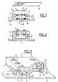
- a reading frameis consisting of support 2 and contact terminations of first type or brush contacts 3 located on the face upper 4 of the support, forming part of a so-called plan upper plane of the frame, and intended to achieve a electrical connection with contact pads 5 of a smart card 20.
- the supporthas a lower face 6, forming part of a plane called the lower plane of the frame, raised relative to a printed circuit 15 and thus delimiting a housing for a component of control 1, the support 2 being secured to the circuit printed 15 by connecting legs 9. From the front lower of the support come out of the contacts 7 realizing direct connection between contact terminations brush 3 and contact pads 8 of component 1.
- FIG. 3a first example of embodiment of an active connector is described in exploded view.
- the insulating support 2comprises cells 22 from which open the brush contacts 3.
- the brush contacts 3are extended by branches 10, 10 'allowing either a direct connection by a connection tab 11 to a corresponding track of the printed circuit, this in the case uncontrolled electrical signals, i.e. a connection to control component 1 via a contact 7 based on a contact pad 8 for signals to pass through this component.
- the contact pads of the control component 1are generally U-shaped and thus achieve a higher contact area and a lower contact pad 18 for connection to the circuit printed.
- Control component 1can include contact pads 18 'not connected to brush contacts 3 and connected only to the circuit printed by 19 'tracks so as to convey the specific signals from the control component such as its power supply or signals to the application.
- the branches 10are optionally mounted floating vertically in the cells 22 and that the latter may include a vertical stop element 21.
- the contact element consisting of the brush contact 3, branch 10 and contact element 8form a spring contact whose efforts are distributed between range 5 of the card and range 8 of the component.
- the 10 'branchescan come out laterally before cutting the lower plane defined by the lower face of the frame in order to be sufficiently spaced laterally from connection areas of the control component.
- the 10 'branchescan also have a part molded into the frame to define their maintenance.
- the supportmay include, in addition to the complementary legs 9 support on the printed circuit possibly extended by a harpoon-type retention device (see item 23 on the example described in Figure 4), support elements 24 and holding component 1.
- Figure 4a second example of embodiment is described for which the brush contacts 3, protruding of the upper plane of the frame, are part of an element of three-pronged contact comprising in its part lower than the lower plane of the frame, on the one hand, a connecting branch 10 'for connection to the printed circuit by a tab 11 and, on the other hand, a lateral branch 12 terminated by the termination of contact 8.
- the lateral branches 12form component 1 support spring on the printed circuit
- the contact elementscan either include a zone support molded into the insulating support 2, or be trapped in the insulating support which, in this case, will be carried out in two parts.
- the connecting legs 9are provided with a retention 23 on the printed circuit and the support insulator has walls 24 for centering the support relative to the component.
- Componentcan be soldered on the printed circuit before mounting the frame of reading, or the whole support / reading frame can be mounted in one operation, the cells 22 being of sufficient size for visual inspection of soldering of the areas 18 on the printed circuit either possible.
- the signalsare accessible at the level of the printed circuit by butts 13.
- the componentmay have no contact patch on its underside. Versions for which one of the three branches of certain contact elements can being omitted optimizes the links and does not render accessible at the PCB level that the signals useful while remaining within the scope of the invention.
- the welds of the different legs or ranges of connection to the printed circuitcan be made according to the usual flat transfer techniques of electronic components.
Landscapes
- Engineering & Computer Science (AREA)
- Artificial Intelligence (AREA)
- Computer Vision & Pattern Recognition (AREA)
- Physics & Mathematics (AREA)
- General Physics & Mathematics (AREA)
- Theoretical Computer Science (AREA)
- Coupling Device And Connection With Printed Circuit (AREA)
Description
Translated fromFrenchL'invention concerne un connecteur actif pourcarte à microcircuit (ou carte à puce) c'est-à-dire unconnecteur pour carte à puce comportant un composant decontrôle d'opérations de lecture / écriture de la carteassocié à un cadre de lecture comportant un support etdes terminaisons de contact avec la carte à puce.The invention relates to an active connector formicrocircuit card (or smart card), i.e. asmart card connector with a componentcontrol of card read / write operationsassociated with a reading frame comprising a support andcontact terminations with the smart card.
Les cadres de lecture pour carte à puce de typeconnu comportent des terminaisons de contact communémentappelées contacts balais destinées à relier les plagesde contact de la carte, par exemple carte à mémoireutilisée dans les applications bancaires, téléphonespublics, téléphones cellulaires ou autres, à uneélectronique de traitement des informations contenuesdans la carte.Reading frames for smart card typeknown have commonly used contact terminationscalled brush contacts intended to connect the padscard contact, e.g. memory cardused in banking applications, phonespublic, cell phones or other, at aelectronic data processingin the map.
Dans les systèmes connus, le concepteurd'applications utilisant des cartes à puce doit prévoird'une part les circuits électroniques de son applicationmais aussi les dispositifs de gestion directe de lalecture / écriture de la carte d'où accroissement descontraintes en terme d'encombrement de son appareil etun coût supplémentaire en temps de développement, testet composants utilisés. En outre, cette conceptioncomporte le risque d'accroítre les longueurs deconnexion, ce qui est défavorable en terme de hautefréquence et de susceptibilité aux perturbationsélectromagnétiques et en terme de rayonnement propre.In known systems, the designerof applications using smart cards should provideon the one hand the electronic circuits of its applicationbut also the devices for direct management of theread / write of the card hence increasedconstraints in terms of the size of its device andadditional cost in development time, testingand components used. Furthermore, this designcarries the risk of increasing the lengths ofconnection, which is unfavorable in terms of highfrequency and susceptibility to disturbanceelectromagnetic and in terms of clean radiation.
La complexité croissante des protocoles degestion de lecture / écriture de la carte et lanécessité d'accroítre la sécurité des opérationseffectuées avec la carte conduit par ailleurs lesconstructeurs de circuits intégrés à réaliser descomposants déchargeant le concepteur d'applicationsélectroniques utilisant des cartes à puce de la gestion des séquences ou protocoles de lecture / écriture desinformations sur la carte.The increasing complexity ofcard read / write management andneed to increase operational securitycarried out with the card also leads theintegrated circuit manufacturers to realizecomponents offloading the application designermanagement using smart cardssequences or protocols for reading / writingcard information.
Dans la demande de brevetinternationale WO 96/24111, qui fait partie de l'état de la technique dans le sens del'article 54(3) CBE,lademanderesse décrit la réalisation d'un connecteur pourcarte à puce incorporant un composant de contrôle dontdes plages d'entrées-sorties sont interposées entrecertaines des terminaisons de raccordement au circuitimprimé de l'application électronique et certains descontacts balais par l'intermédiaire d'un réseau deconnexions.In the patent applicationWO 96/24111, which is part of the state of the art in the sense ofArticle 54 (3) EPC,theApplicant describes the production of a connector forsmart card incorporating a control component includinginput-output ranges are interposed betweensome of the circuit connection terminationsprinted from the electronic application and some of thebrush contacts through a network ofconnections.
La présente invention a pour but de proposer unenouvelle conception de connecteur actif d'intégrationpoussée présentant l'avantage de minimiser les longueursdes liaisons électriques défavorables pour des signauxrapides.The object of the present invention is to provide anew active integration connector designthrust with the advantage of minimizing lengthsunfavorable electrical connections for signalsfast.
Dans ce but, l'invention propose d'intégrerdirectement un composant de contrôle sous un cadre delecture.. et prévoit pour cela de réaliser un connecteurpour carte à puce principalement constitué d'uncomposant de contrôle d'opérations de lecture / écriturede la carte à puce et d'un cadre de lecture pour carte àpuce, le cadre de lecture comportant un support enmatériau isolant recevant des terminaisons de contactd'un premier type faisant saillie d'un plan supérieur dusupport en matériau isolant pour être en contactélectrique avec les plages de contact de la carte, pourlequel le support isolant comporte un plan inférieur,duquel font saillie, d'une part, des terminaisons decontact d'un deuxième type pour être en contactélectrique avec des plages de contact du composant decontrôle d'opérations de lecture / écriture de la carteet, d'autre part, des jambes de liaison sur un circuitimprimé dont la hauteur h définit un espace entre lesupport isolant et le circuit imprimé tel que lecomposant de contrôle soit logé entre le plan inférieurdu support isolant et le circuit imprimé.To this end, the invention proposes to integratedirectly a control component under a framework ofreading .. and plans to make a connector for thisfor smart card mainly consisting ofread / write operations control componentof the smart card and a reading frame for a smart cardpuce, the reading frame comprising a supportinsulating material receiving contact terminationsof a first type projecting from an upper plane of thesupport in insulating material to be in contactelectric with the contact areas of the card, forwhich the insulating support has a lower plane,from which protrude, on the one hand, endings ofcontact of a second type to be in contactelectrical with contact pads of the componentcontrol of card read / write operationsand, on the other hand, connecting legs on a circuitprint whose height h defines a space between theinsulating support and the printed circuit such ascontrol component is housed between the lower planeof the insulating support and the printed circuit.
Selon d'autres caractéristiques et modes deréalisation de l'invention :
- une ou plusieurs des terminaisons de contactdu premier type sont prolongées par des branches lesreliant à des terminaisons de contact du deuxième typecorrespondantes pour réaliser une liaison directe entredes plages de contact de la carte à puce et des plagesde contact du composant de contrôle ;
- les jambes de liaisons sont constituées despattes de connexion électrique d'une ou plusieurs desterminaisons de contact du premier type avec le circuitimprimé ;
- une ou plusieurs pattes de connexion peuventposséder une branche latérale de liaison avec desterminaisons de contact du deuxième type ;
- la hauteur des jambes de liaison est telle queles branches latérales soient mises en pression sur lesplages de contact respectives du composant de contrôleassurant ainsi la liaison électrique et le maintienmécanique du composant de contrôle entre le connecteuret le circuit imprimé ;
- une ou plusieurs des terminaisons de contactdu deuxième type peuvent comporter une portion ressortd'accrochage et de maintien du composant de contrôlecontre la face inférieure du support isolant, la portionressort assurant la mise en pression des deuxièmesterminaisons de contact avec les plages de contact ducomposant de contrôle ;
- - le support isolant comporte des butéesd'insertion du composant de contrôle sous le supportisolant ;
- les terminaisons de contact du premier type etles terminaisons de contact du deuxième type sontconstituées par les parties terminales, respectivementsupérieure et inférieure, de forme générale courbe, delames de contact électrique débouchant respectivement en partie supérieure et en partie inférieure du supportisolant, la face externe de la partie terminalesupérieure étant en contact élastique avec une plagecorrespondante de la carte à puce, la face interne de lapartie terminale inférieure étant en contact élastiqueavec une plage correspondante du composant de contrôleet la face externe de la partie terminale inférieureétant en contact avec une piste correspondante ducircuit imprimé.
- one or more of the contact endings of the first type are extended by branches connecting them to contact endings of the second type corresponding to make a direct connection between contact pads of the smart card and contact pads of the control component ;
- the connecting legs consist of the electrical connection lugs of one or more of the contact terminations of the first type with the printed circuit;
- one or more connection lugs may have a lateral branch for connection with contact terminations of the second type;
- the height of the connecting legs is such that the lateral branches are pressurized on the respective contact pads of the control component, thus ensuring the electrical connection and the mechanical maintenance of the control component between the connector and the printed circuit;
- one or more of the contact ends of the second type may include a spring portion for hooking and holding the control component against the underside of the insulating support, the spring portion ensuring the pressurization of the second contact ends with the pads contact of the control component;
- - The insulating support includes stops for inserting the control component under the insulating support;
- the contact terminations of the first type and the contact terminations of the second type consist of the terminal parts, respectively upper and lower, of generally curved shape, of electrical contact blades opening out respectively in the upper part and in the lower part of the insulating support, the external face of the upper end part being in elastic contact with a corresponding area of the smart card, the internal face of the lower end part being in elastic contact with a corresponding area of the control component and the external face of the end part lower being in contact with a corresponding track of the printed circuit.
D'autres caractéristiques et avantages del'invention apparaítront à la lecture de la descriptionqui va suivre en référence avec les dessins annexés quireprésentent ;
- en figure 1 une vue latérale d'un connecteuractif selon le principe de l'invention ;
- en figures 2, 4, 5 des vues latérales en couped'un connecteur actif selon plusieurs modes deréalisation de l'invention ;
- en figure 3 une vue du dessus en perspectivepartiellement éclatée d'une variante de réalisation del'invention ;
- en figure 6 une vue du dessous partiellementéclatée d'un mode de réalisation particulier del'invention.
- in Figure 1 a side view of an active connector according to the principle of the invention;
- in Figures 2, 4, 5 side sectional views of an active connector according to several embodiments of the invention;
- in Figure 3 a partially exploded perspective view from above of an alternative embodiment of the invention;
- in Figure 6 a partially exploded view from below of a particular embodiment of the invention.
Le principe du connecteur selon l'invention estschématisé en figure 1. Un cadre de lecture estconstitué du support 2 et des terminaisons de contact dupremier type ou contacts balais 3 situés sur la facesupérieure 4 du support, s'inscrivant dans un plan ditplan supérieur du cadre, et destinés à réaliser uneconnexion électrique avec des plages de contact 5 d'unecarte à puce 20. Le support comporte une face inférieure6, s'inscrivant dans un plan dit plan inférieur ducadre, surélevée par rapport à un circuit imprimé 15 etdélimitant ainsi un logement pour un composant decontrôle 1, le support 2 étant solidarisé au circuit imprimé 15 par des jambes de liaison 9. De la faceinférieure du support sortent des contacts 7 réalisantune connexion directe entre des terminaisons de contactbalai 3 et des plages de contact 8 du composant 1.The principle of the connector according to the invention isshown schematically in Figure 1. A reading frame isconsisting of
En figure 3 un premier exemple de réalisationd'un connecteur actif est décrit en vue éclatée. Lesupport isolant 2 comporte des alvéoles 22 d'oùdébouchent les contacts balais 3. Les contacts balais 3sont prolongés par des branches 10, 10' permettant soitune liaison directe par une patte de connexion 11 à unepiste correspondante du circuit imprimé, ce dans le casde signaux électriques non contrôlés, soit une connexionau composant de contrôle 1 par l'intermédiaire d'uncontact 7 reposant sur une plage de contact 8 pour lessignaux devant transiter par ce composant. Selon le modede réalisation de la figure 3, les plages de contact ducomposant de contrôle 1 sont de forme générale en U etréalisent ainsi une plage de contact supérieure et uneplage de contact inférieure 18 de connexion au circuitimprimé. Cette forme en U donne l'avantage de simplifierla réalisation du composant de contrôle par rapport àune réalisation pour laquelle le composant de contrôleest muni de plages supérieures et inférieures commedécrit en figure 1. Cette configuration permet uneéventuelle lecture des signaux de contrôle au niveau ducircuit imprimé. Le composant de contrôle 1 peutcomporter des plages de contact 18' non reliées auxcontacts balais 3 et reliées uniquement au circuitimprimé par des pistes 19' de manière à véhiculer lessignaux spécifiques du composant de contrôle tels queson alimentation ou les signaux à destination del'application. Sur la figure 3 on peut voir que lesbranches 10 sont éventuellement montées flottantesverticalement dans les alvéoles 22 et que ces dernièrespeuvent comporter un élément de butée verticale 21. Dansce cas, l'élément de contact constitué du contact balai 3, de la branche 10 et de l'élément de contact 8 formeun contact ressort dont les efforts sont répartis entrela plage 5 de la carte et la plage 8 du composant. Pource qui concerne les contacts balais reliés directementau circuit imprimé par des pattes des connexions 11, lesbranches 10' peuvent sortir latéralement avant de couperle plan inférieur défini par la face inférieure du cadreafin d'être suffisamment espacées latéralement desplages de connexion du composant de contrôle. Lesbranches 10' peuvent de plus comporter une partiesurmoulée dans le cadre pour définir leur maintien. Lesupport peut comporter, outre les jambes complémentaires9 d'appui sur le circuit imprimé éventuellementprolongées par un dispositif de rétention de type harpon(voir repère 23 sur l'exemple décrit en figure 4), deséléments d'appui 24 et de maintien du composant 1.In Figure 3 a first example of embodimentof an active connector is described in exploded view. The
En figure 4 un deuxième exemple de réalisationest décrit pour lequel les contacts balais 3, dépassantdu plan supérieur du cadre, font partie d'un élément decontact à trois branches comportant dans sa partieinférieure au plan inférieur du cadre, d'une part, unebranche de liaison 10' de connexion au circuit imprimépar une patte 11 et, d'autre part, une branche latérale12 terminée par la terminaison de contact 8. Dans cemode de réalisation, les branches latérales 12 formentressort d'appui du composant 1 sur le circuit imprimé,les éléments de contact pouvant soit comporter une zonede maintien surmoulée dans le support isolant 2, soitêtre emprisonnés dans le support isolant qui, dans cecas, sera réalisé en deux parties. Avantageusement, lesjambes de liaison 9 sont pourvues d'un élément derétention 23 sur le circuit imprimé et le supportisolant comporte des parois 24 de centrage du supportpar rapport au composant. Le composant peut être soudésur le circuit imprimé préalablement au montage du cadrede lecture, ou l'ensemble support / cadre de lecture peut être monté en une opération, les alvéoles 22 étantde taille suffisante pour qu'un contrôle visuel dessoudures des plages 18 sur le circuit imprimé soitpossible.In Figure 4 a second example of embodimentis described for which the
En figures 5 et 6 est décrit une exemple deréalisation alternatif pour lequel le composant 1 estretenu sous le support isolant. Les éléments de contact7 sont alors soit la terminaison d'un contact ressort encrosse assurant la rétention du composant et réalisantla connexion par sa face externe 13 au circuit imprimécomme vu en figure 6, soit prolongés par une patte deconnexion 11 comme vu en figure 5. L'insertion et lemaintien en position du composant 1 sont permis par desbutées 14, par exemple munies d'un plan incliné pourpermettre l'insertion du composant et d'une butéefranche dans le sens extraction du composant.In Figures 5 and 6 is described an example ofalternative production for which
Dans l'exemple des figures 5 et 6, les signauxsont accessibles au niveau du circuit imprimé par lescrosses 13. Dans l'exemple décrit en figure 4, lecomposant peut ne comporter aucune plage de contact sursa face inférieure. Des versions pour lesquelles l'unedes trois branches de certains éléments de contacts peutêtre omise permet d'optimiser les liaisons et ne rendreaccessibles au niveau du circuit imprimé que les signauxutiles tout en restant dans le cadre de l'invention.In the example of Figures 5 and 6, the signalsare accessible at the level of the printed circuit by
Les soudures des différentes pattes ou plages deconnexion sur le circuit imprimé pourront être réaliséesselon les techniques habituelles de report à plat decomposants électroniques.The welds of the different legs or ranges ofconnection to the printed circuit can be madeaccording to the usual flat transfer techniques ofelectronic components.
Claims (8)
- Active connector for a smart card consisting of acomponent (1) for controlling read/write operations forthe smart card (20) and a reading frame for a smartcard comprising a support (2) made of an insulatoraccommodating contact terminations of a first type (3)projecting from an upper plane (4) of the support madeof an insulator in order to be in electrical contactwith contact pads (5) on the smart card, the saidinsulating support comprising a lower face (6) comingwithin a lower plane, from which project, on the onehand, contact terminations of a second type (7) inorder to be in electrical contact with the contact pads(8) on the component controlling read/write operationsof the smart card and, on the other hand, legs (9, 11)for connection to a printed circuit whose height (h)defines a space between the insulating support and theprinted circuit (15) such that the control component ishoused between the lower plane of the insulatingsupport and the printed circuit.
- Active connector for a smart card according toClaim 1,characterized in that one or more of thecontact terminations of the first type (3) are extendedby arms (10) connecting them to corresponding contactterminations of the second type (7) in order to make adirect connection between contact pads (5) on the smartcard and contact pads on the control component.
- Active connector for a smart card according toeither of Claims 1 and 27characterized in that some ofthe connection legs consist of arms (10') terminated bylugs (11) for electrically connecting one or more ofthe contact terminations of the first type with tracksof the printed circuit (15).
- Active connector for a smart card according toClaim 3,characterized in that one or more connectionlugs have a side arm (12) for connection with contactterminations of the second type.
- Active connector for a smart card according toClaim 4,characterized in that the height of theconnection legs is such that the side arms (12) arepressed against the respective contact pads (8) on thecontrol component thus providing the electricalconnection and the mechanical holding of the controlcomponent between the connector and the printedcircuit.
- Active connector for a smart card according to anyone of Claims 1 to 3,characterized in that one or moreof the contact terminations of the second type comprisea spring portion (13) for fastening and holding thecontrol component against the lower face (6) of theinsulating support, the spring portion ensuring thatthe second contact terminations are pressed against thecontact pads on the control component.
- Active connector for a smart card according toClaim 6,characterized in that the contact terminationsof the first type and the contact terminations of thesecond type consist of upper and lower terminal partsrespectively, of overall curved shape, havingelectrical contact strips emerging respectively fromthe upper part and from the lower part of theinsulating support, the outer face of the upper terminal part being in elastic contact with acorresponding pad on the smart cards the inner face ofthe lower terminal part being in elastic contact with acorresponding pad on the control component and theouter face of the lower terminal part being in contactwith a corresponding track on the printed circuit.
- Active connector for a smart card according to anyone of the preceding claims,characterized in that theinsulating support comprises stops (14) for insertingthe control component under the insulating support.
Applications Claiming Priority (2)
| Application Number | Priority Date | Filing Date | Title |
|---|---|---|---|
| FR9515666AFR2743170B1 (en) | 1995-12-28 | 1995-12-28 | ACTIVE CONNECTOR FOR CHIP CARD |
| FR9515666 | 1995-12-28 |
Publications (2)
| Publication Number | Publication Date |
|---|---|
| EP0782088A1 EP0782088A1 (en) | 1997-07-02 |
| EP0782088B1true EP0782088B1 (en) | 2003-03-26 |
Family
ID=9486088
Family Applications (1)
| Application Number | Title | Priority Date | Filing Date |
|---|---|---|---|
| EP96402598AExpired - LifetimeEP0782088B1 (en) | 1995-12-28 | 1996-11-29 | Active connector for chip card |
Country Status (5)
| Country | Link |
|---|---|
| US (1) | US5902152A (en) |
| EP (1) | EP0782088B1 (en) |
| JP (1) | JPH09199243A (en) |
| DE (1) | DE69626945T2 (en) |
| FR (1) | FR2743170B1 (en) |
Families Citing this family (12)
| Publication number | Priority date | Publication date | Assignee | Title |
|---|---|---|---|---|
| EP0726620B1 (en)* | 1995-02-07 | 2003-06-18 | Johnstech International Corporation | Apparatus for providing controlled impedance in an electrical contact |
| JP2001015194A (en)* | 1999-05-05 | 2001-01-19 | Thomas & Betts Corp <T&B> | Improved smart card reader used at dispositions elevated from printed circuit board |
| FR2800923A1 (en) | 1999-11-08 | 2001-05-11 | Framatome Connectors Int | MICRO-CIRCUIT CARD READER |
| DE10006445C2 (en)* | 2000-02-14 | 2002-03-28 | Infineon Technologies Ag | Intermediate frame for a housing frame of semiconductor chips |
| FR2805671B1 (en)* | 2000-02-25 | 2002-07-26 | Sagem | CONNECTOR FOR CHIP CARDS |
| US6508673B2 (en) | 2000-04-05 | 2003-01-21 | Mcdowell Jennifer Lyn | Low cost smart card reader, extension style, with wiping contacts |
| ATE354135T1 (en)* | 2002-09-25 | 2007-03-15 | Koninkl Philips Electronics Nv | CHIP CARD CONNECTOR |
| US7110237B2 (en)* | 2003-05-01 | 2006-09-19 | Eastman Kodak Company | Apparatus and method to reduce static charge on removable media |
| JP4744791B2 (en)* | 2003-06-23 | 2011-08-10 | パナソニック株式会社 | Surface mount type electronic component and electronic circuit device using the same |
| GB2422253A (en)* | 2005-01-18 | 2006-07-19 | Nokia Corp | Electronic component pin connector with aperture for filter |
| US20070278467A1 (en)* | 2006-05-30 | 2007-12-06 | Ash Corey D | Fencing system capable of adjusting to a sloping ground |
| JP4735999B2 (en)* | 2009-04-03 | 2011-07-27 | 株式会社デンソー | Connector fixing structure for in-vehicle control device |
Family Cites Families (12)
| Publication number | Priority date | Publication date | Assignee | Title |
|---|---|---|---|---|
| US4089575A (en)* | 1976-09-27 | 1978-05-16 | Amp Incorporated | Connector for connecting a circuit element to the surface of a substrate |
| US4447716A (en)* | 1982-03-01 | 1984-05-08 | Seiichiro Aigo | Information card |
| FR2587549B1 (en)* | 1985-09-13 | 1988-03-04 | Radiotechnique | INTERCONNECTION SYSTEM |
| US4871316A (en)* | 1988-10-17 | 1989-10-03 | Microelectronics And Computer Technology Corporation | Printed wire connector |
| US4993956A (en)* | 1989-11-01 | 1991-02-19 | Amp Incorporated | Active electrical connector |
| US5258411A (en)* | 1990-10-15 | 1993-11-02 | Exxon Research And Engineering Co. | Activation conditions to maximize the HCS activity of supported cobalt catalysts (OP-3706) |
| US5118300A (en)* | 1991-05-23 | 1992-06-02 | Amp Incorporated | Active electrical connector |
| EP0520080B2 (en)* | 1991-06-28 | 2005-03-30 | Molex Incorporated | IC card connector |
| US5309324A (en)* | 1991-11-26 | 1994-05-03 | Herandez Jorge M | Device for interconnecting integrated circuit packages to circuit boards |
| US5378160A (en)* | 1993-10-01 | 1995-01-03 | Bourns, Inc. | Compliant stacking connector for printed circuit boards |
| FR2720869B1 (en)* | 1994-06-01 | 1996-07-12 | Itt Composants Instr | Advanced electrical connector for connecting an electronic memory card. |
| FR2730328B1 (en)* | 1995-02-03 | 1997-04-04 | Connectors Pontarlier | CONNECTOR FOR MICROCIRCUIT CARD READING APPARATUS AND MICROCIRCUIT CARD READING APPARATUS INCLUDING SAME |
- 1995
- 1995-12-28FRFR9515666Apatent/FR2743170B1/ennot_activeExpired - Fee Related
- 1996
- 1996-11-29EPEP96402598Apatent/EP0782088B1/ennot_activeExpired - Lifetime
- 1996-11-29DEDE69626945Tpatent/DE69626945T2/ennot_activeExpired - Fee Related
- 1996-12-20USUS08/772,151patent/US5902152A/ennot_activeExpired - Fee Related
- 1996-12-26JPJP8348967Apatent/JPH09199243A/enactivePending
Also Published As
| Publication number | Publication date |
|---|---|
| DE69626945D1 (en) | 2003-04-30 |
| FR2743170B1 (en) | 1998-02-06 |
| DE69626945T2 (en) | 2003-12-11 |
| JPH09199243A (en) | 1997-07-31 |
| US5902152A (en) | 1999-05-11 |
| FR2743170A1 (en) | 1997-07-04 |
| EP0782088A1 (en) | 1997-07-02 |
Similar Documents
| Publication | Publication Date | Title |
|---|---|---|
| EP0782088B1 (en) | Active connector for chip card | |
| KR100835264B1 (en) | Connector for a Module | |
| FR2809871A1 (en) | ELECTRICAL CONNECTOR WITH IMPROVED CONTACT BLADES FOR CONNECTION OF AN INTEGRATED CIRCUIT (S) CARD | |
| FR2494505A1 (en) | ELECTRICAL CONNECTOR CONTACTS FOR WIRELESS CIRCUIT BOARDS | |
| EP0274288B1 (en) | Connection unit for electronic memory cards, and reading/writing device using the same | |
| EP0424263B1 (en) | Chip card system with offset, portable electronic unit | |
| KR19990013511A (en) | Electrical switch assembly | |
| EP1231560B1 (en) | Positioning and holding device for a IC card | |
| FR2587549A1 (en) | Interconnection system | |
| FR2773244A1 (en) | SWITCH FOR DETECTING THE PRESENCE OF AN ELECTRONIC MEMORY CARD IN A READ-WRITE DEVICE | |
| FR2771834A1 (en) | ELECTRICAL CONNECTION DEVICE FOR COOPERATING WITH A MOBILE ELECTRONIC MEDIUM | |
| EP0711438B1 (en) | Electric connector for connecting an electronic smart card including a built-in switch for detecting the presence of a card | |
| WO2012076396A1 (en) | Contact for a microcircuit card connector and use of such contacts | |
| FR2533337A1 (en) | RECORDER-PLAYER AND COMPUTER, IN PARTICULAR MICROCOMPUTER, COMPRISING SUCH A RECORDER-READER | |
| EP1079324A1 (en) | Electronic apparatus comprising a group of smart cards | |
| EP0704092A1 (en) | Electronic memory device | |
| EP0711440B1 (en) | Electric connector for connecting an electronic smart card | |
| US6957965B2 (en) | Electrical connector assembly with a transfer member | |
| US20040209519A1 (en) | Electric connector | |
| EP1019864A1 (en) | Card reader connector, with elastic brush contacts, and reader comprising same | |
| FR2796203A1 (en) | CONTACTLESS ELECTRONIC MODULE AND METHOD FOR OBTAINING THE SAME | |
| FR2824426A1 (en) | COAXIAL ELECTRICAL CONNECTOR ELEMENT | |
| FR2843654A1 (en) | Electrical connector for mounting on circuit board, has laterally spaced columns of contacts, and termination ends of contacts in two columns lie in single longitudinally-extending row | |
| EP2202677B1 (en) | Chip card and mobile terminal comprising such a card | |
| FR2904151A1 (en) | ELECTRONIC MODULE WITH CONNECTOR WITH CONTACT ELASTICAL LEGS, CONNECTOR AND CORRESPONDING CARDS |
Legal Events
| Date | Code | Title | Description |
|---|---|---|---|
| PUAI | Public reference made under article 153(3) epc to a published international application that has entered the european phase | Free format text:ORIGINAL CODE: 0009012 | |
| AK | Designated contracting states | Kind code of ref document:A1 Designated state(s):BE DE GB IT NL SE | |
| 17P | Request for examination filed | Effective date:19971204 | |
| GRAH | Despatch of communication of intention to grant a patent | Free format text:ORIGINAL CODE: EPIDOS IGRA | |
| GRAH | Despatch of communication of intention to grant a patent | Free format text:ORIGINAL CODE: EPIDOS IGRA | |
| RAP1 | Party data changed (applicant data changed or rights of an application transferred) | Owner name:FCI | |
| RBV | Designated contracting states (corrected) | Designated state(s):DE GB IT | |
| GRAA | (expected) grant | Free format text:ORIGINAL CODE: 0009210 | |
| RIC1 | Information provided on ipc code assigned before grant | Ipc:7H 01R 12/22 B Ipc:7G 06K 7/06 A | |
| AK | Designated contracting states | Designated state(s):DE GB IT | |
| REG | Reference to a national code | Ref country code:GB Ref legal event code:FG4D Free format text:NOT ENGLISH | |
| REF | Corresponds to: | Ref document number:69626945 Country of ref document:DE Date of ref document:20030430 Kind code of ref document:P | |
| GBT | Gb: translation of ep patent filed (gb section 77(6)(a)/1977) | ||
| PLBE | No opposition filed within time limit | Free format text:ORIGINAL CODE: 0009261 | |
| STAA | Information on the status of an ep patent application or granted ep patent | Free format text:STATUS: NO OPPOSITION FILED WITHIN TIME LIMIT | |
| 26N | No opposition filed | Effective date:20031230 | |
| PGFP | Annual fee paid to national office [announced via postgrant information from national office to epo] | Ref country code:GB Payment date:20051004 Year of fee payment:10 | |
| PG25 | Lapsed in a contracting state [announced via postgrant information from national office to epo] | Ref country code:IT Free format text:LAPSE BECAUSE OF NON-PAYMENT OF DUE FEES Effective date:20051129 | |
| PGFP | Annual fee paid to national office [announced via postgrant information from national office to epo] | Ref country code:DE Payment date:20051130 Year of fee payment:10 | |
| PG25 | Lapsed in a contracting state [announced via postgrant information from national office to epo] | Ref country code:DE Free format text:LAPSE BECAUSE OF NON-PAYMENT OF DUE FEES Effective date:20070601 | |
| GBPC | Gb: european patent ceased through non-payment of renewal fee | Effective date:20061129 | |
| PG25 | Lapsed in a contracting state [announced via postgrant information from national office to epo] | Ref country code:GB Free format text:LAPSE BECAUSE OF NON-PAYMENT OF DUE FEES Effective date:20061129 |