EP0780014B1 - Security device - Google Patents
Security deviceDownload PDFInfo
- Publication number
- EP0780014B1 EP0780014B1EP95930608AEP95930608AEP0780014B1EP 0780014 B1EP0780014 B1EP 0780014B1EP 95930608 AEP95930608 AEP 95930608AEP 95930608 AEP95930608 AEP 95930608AEP 0780014 B1EP0780014 B1EP 0780014B1
- Authority
- EP
- European Patent Office
- Prior art keywords
- security device
- circuit means
- substrate
- fixing portion
- adhesive layer
- Prior art date
- Legal status (The legal status is an assumption and is not a legal conclusion. Google has not performed a legal analysis and makes no representation as to the accuracy of the status listed.)
- Expired - Lifetime
Links
- 239000010410layerSubstances0.000claimsdescription26
- 239000012790adhesive layerSubstances0.000claimsdescription21
- 239000000758substrateSubstances0.000claimsdescription13
- OKTJSMMVPCPJKN-UHFFFAOYSA-NCarbonChemical compound[C]OKTJSMMVPCPJKN-UHFFFAOYSA-N0.000claimsdescription5
- 239000000853adhesiveSubstances0.000claimsdescription5
- 230000001070adhesive effectEffects0.000claimsdescription5
- 229910052799carbonInorganic materials0.000claimsdescription5
- 230000001419dependent effectEffects0.000claimsdescription2
- 239000000976inkSubstances0.000description10
- BQCADISMDOOEFD-UHFFFAOYSA-NSilverChemical compound[Ag]BQCADISMDOOEFD-UHFFFAOYSA-N0.000description4
- 229910052709silverInorganic materials0.000description4
- 239000004332silverSubstances0.000description4
- 238000003892spreadingMethods0.000description3
- 238000012544monitoring processMethods0.000description2
- 229920000728polyesterPolymers0.000description2
- 230000035945sensitivityEffects0.000description2
- 230000001960triggered effectEffects0.000description2
- 239000004593EpoxySubstances0.000description1
- 239000003522acrylic cementSubstances0.000description1
- 238000009826distributionMethods0.000description1
- 230000000694effectsEffects0.000description1
- 239000011810insulating materialSubstances0.000description1
- 238000004519manufacturing processMethods0.000description1
- 239000000463materialSubstances0.000description1
- 239000004033plasticSubstances0.000description1
- 229920003023plasticPolymers0.000description1
- 229920000515polycarbonatePolymers0.000description1
- 239000004417polycarbonateSubstances0.000description1
- 238000003825pressingMethods0.000description1
- 239000000126substanceSubstances0.000description1
Images


Classifications
- G—PHYSICS
- G08—SIGNALLING
- G08B—SIGNALLING OR CALLING SYSTEMS; ORDER TELEGRAPHS; ALARM SYSTEMS
- G08B13/00—Burglar, theft or intruder alarms
- G08B13/02—Mechanical actuation
- G08B13/14—Mechanical actuation by lifting or attempted removal of hand-portable articles
- G08B13/1445—Mechanical actuation by lifting or attempted removal of hand-portable articles with detection of interference with a cable tethering an article, e.g. alarm activated by detecting detachment of article, breaking or stretching of cable
Definitions
- the present inventionrelates to a security device for fixing to a surface to allow relative movement of the device and the surface to be detected, and a connector for such a device.
- a known device used for this purposecomprises a flexible body having a head and a tail.
- One side of the headbears an adhesive layer for fixing the device to a surface (which is suitably the surface of a displayed items.
- An electrically conductive stripwhich may have some resistance, passes from one contact at the distal end of the tail, across the head (where it lies between the body and the adhesive layer) and back to another contact at the distal end of the tail.
- the adhesive layeris in two separate inner and outer regions. The conductive strip overlying the outer region is adhered firmly to the body and to the adhesive layer.
- the conductive strip overlying the inner regionis adhered to the adhesive but a non-adhesive layer lies between the inner region and the body.
- alarm apparatusis connected to the contacts to monitor the resistance between them. If an attempt is made to lift the head of the device off the surface the inner region and the portion of the conductive strip overlying it remain adhered to the surface whilst the outer region and the remainder of the conductive strip are lifted. This breaks the circuit and triggers the alarm.
- This devicehas several problems, for example:
- WO 94/14142discloses a similar device, which is, however, not easily manufactured.
- US-A-4000488discloses a similar device, which is, however, not very reliable.
- a security deviceis provided with the features claimed in claim 1.
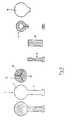
- the device shown in Figures 1 to 3has a flexible laminar upper member 1 having a head portion 2 and an elongate tail 3.
- a frangible, electrically conductive track 4passes from a contact 5 at the distal end of the tail, down the tail, around the head near its periphery and back to a contact 6.
- Between the track and the headlie three regions 7 of a release layer which bonds relatively weakly to the upper member.
- An adhesive layer 8for fixing the head to a surface, underlies the release layer and the track. The bond directly between the adhesive layer and the track is weaker than that directly between the track and the upper member but stronger than that directly between the release layer and the upper member.
- the upper memberis made of a thin, flexible sheet which can be printed on and which provides a substrate to bear the other layers.
- the upper membercould be made of polyester (particularly heat-stabilised polyester), PVC, polycarbonate or paper.
- On the upper surface of the upper memberare printed opaque, hard wearing, scuff-resistant inks to suitably decorate the surface and hide the lower layers from view when the device is fixed to a surface.
- the release layeris a layer of a delaminating substance, for example a peelable ink (such as Coates Lorilleux COSOL 19-75 black) or a combination of inks, printed on the lower surface of the upper member.
- the release layerbonds relatively weakly to the upper member and the conductive track.
- the release layeris preferably relatively brittle and/or sensitive to stress so that if any part of the head is deformed, for example as an attempt is made to pull its edge from a surface, or if the substrate is pulled away from the adhesive layer the release layer (or at least part of it) will shatter and/or delaminate and/or release from the upper member or the track and disrupt the conductive track (suitably by breaking the track completely at at least one point).
- the release layeris divided radially into three regions so that there are several locations where adjacent portions of the track are bonded directly to the upper member and directly to the release layer. The track is most likely to be disrupted at these locations. Three radially disposed regions of release layer have been found to give a suitable sensitivity to the device.
- the conductive trackis formed of a conductive ink, for example a carbon-bearing ink, and has a resistance.
- the conductive trackhas a very low resistance and is made, for example of a silver-loaded ink.
- the silver-loaded inkis coated on its lower surface with carbon to prevent the silver from corroding and provide the contacts to which monitoring apparatus may be connected when the device is in use.
- An alarmcan be made to sound if the circuit is disrupted and there is a change in the resistance: either an increase if the track is broken or damaged or a decrease if the resistive portion of the carbon track is short-circuited (by a conductive implement, such as a blade, being used to remove the device).
- the conductive trackextends substantially all around the head, and near the periphery of the head, to increase the sensitivity of the device to lifting of any part of the periphery of the head from the surface.
- An insulating dielectric layer 11 made of insulating inkcovers the lower surface of the conductive track along the tail to protect the track from accidental shorting and to prevent the device from being shorted by a thief connecting the correct resistance across the tracks in the tail (this might otherwise allow the device to be removed from the surface without the alarm being triggered).
- the adhesive layerhas a tissue carrier (not shown in the figures) and is suitably chosen to have instant, strong adhesion to a surface and to be capable of conforming and/or adhering well to textured surface surfaces.
- the adhesivemay be an epoxy or acrylic adhesive.
- the adhesive usedmust be compatible with the other layers. Suitable adhesives are, for example, Technibond 370 or T555.
- the headis suitably generally disc-shaped with a diameter of around 28mm.
- the conductive trackis suitably around 2mm wide and the gaps between adjacent regions of the release layer are suitably around 1mm wide.
- the gap between the track and the outer edge of the release layeris suitably around 2mm.
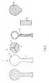
- the device shown in Figure 4is generally similar to that of Figures 1 to 3 and like parts are numbered in Figure 4 as for Figures 1 to 3.
- the conductive trackis formed throughout of a conductive silver-loaded ink (having a very low resistance). Contrasted with the devices of Figures 1 to 3 this device has the disadvantage that short-circuiting of it cannot be detected as a significant drop in resistance. However, it has the advantages that it is cheaper to manufacture (because there is no need for the carbon-bearing ink to be printed on the device) and that simpler apparatus can be used to monitor the device when in use (because there is only a need to detect open or closed circuits).
- the device shown in Figure 5has like parts numbered as for Figures 1 to 4.
- the head position 2is in the shape of an elongate strip (this allows the device to be fixed to narrow objects such as the surrounds of video camera lenses) and the tail 3 is shorter than those of the other devices (this reduces the risk of the tail of the device being tampered with to bypass the head).
- the conductive track 4runs around the periphery of the head and the regions 7 of release layer lie in strips laterally across the head, with two partial strips 7a at the top of the head. This configuration has been found to be particularly sensitive.
- the partial stripsare provided to give a closer distribution of the regions of release layer at the top of the head where the device is most easily peelable from a substrate.
- FIG. 6shows a connector suitable for holding the devices shown in the other Figures in contact with wires that lead to monitoring apparatus.
- the connectoris made of insulating material (for example plastics material) and has a base block 12, a contact cover 13 joined to the base block by a hinge 14, and a wiring cover (not shown).
- the base blockhas a generally planar floor from which rise wiring walls 15,16 between which the wires run into the interior of the connector.
- the wiring wallsinclude projections 17 to hold the wires in place. At their interior ends the wiring walls are separated by a spreading wall 18. The two wires pass on either side of the spreading wall and the interior ends of the wires beyond roughly the position of the spreading wall are bared to allow them to make contact with the contacts 5,6 of the devices.
- the wiring cover 15has wings which snap between outer walls 19 of the base block to hold the wires in the connector.
- the bared wire ends(illustrated by chain dotted lines at 20) pass over a first lateral wall 21 raised from the floor of a contact region 22 of the base block.
- the deviceWhen a connection to a device is to be made the device is placed on the base block with its contacts touching the bared wires as they pass over the first lateral wall.
- the shoulders 23 of the deviceabut against the interior edges of retaining walls 24 of the base block so that the device is held captive in the connector when the contact cover 13 is closed.
- the contact coverhas a wing 25 which snaps over a projection 26 on the base block to hold it closed, second lateral walls 27 and a pin 28 which mates with a recess 29 in an annular wall on the base block.
- the second lateral wallsare formed to cooperate with the first lateral wall to press the contacts against the bared wires when the contact cover is closed.
- the pinserves to help hold the device in the connector by pressing against the tail of the device or by passing through a hole 30 in the tail when one is provided. If such a hole is provided it is preferably dimensioned so that the pin is a tight frictional fit in the hole. This has the effect of frictionally adhering the device to the contact cover so that if the contact cover is opened (for instance by someone tampering with the connector) the contacts of the device are lifted from the bared wires and the alarm is triggered. This makes it difficult to gain access to the contacts without triggering the alarm. As a further security feature the connector encloses part of the tail of the device to reduce the risk of the tail being tampered with.
Landscapes
- Physics & Mathematics (AREA)
- General Physics & Mathematics (AREA)
- Burglar Alarm Systems (AREA)
- Alarm Systems (AREA)
- Bidet-Like Cleaning Device And Other Flush Toilet Accessories (AREA)
- Electrical Discharge Machining, Electrochemical Machining, And Combined Machining (AREA)
- Details Of Connecting Devices For Male And Female Coupling (AREA)
- Clamps And Clips (AREA)
Abstract
Description
- it is possible for skilful thieves to prise thewhole device from the surface without triggering thealarm by first lifting the edge of the device and theninserting a tool between the adhesive layer and thesurface, for example from the edge of the head furthestfrom the tail, where the conductive strip does not pass;
- the portions of the conductive strip in the tailare exposed and a thief can therefore bypass the strip inthe head by creating a short circuit of the correctresistance across these portions.
Claims (19)
- A security device for fixing to a surface to allowrelative movement of the device and the surface to bedetected, the device comprising:a substrate (1) having a fixing portion by which thedevice may be fixed to the surface;an adhesive layer (18) for fixing the fixing portion tothe surface; andcircuit means defining an ohmic circuit between twolocations on the device, at least part of the circuitmeans being located between the substrate (1) and theadhesive layer (8) and having in a first region a greateradhesion with the substrate (1) than with the adhesive layer (8)and in a second region a greater adhesion with theadhesive layer (8) than with the substrate (1) to allow relativemovement of the substrate (1) and the surface, and, when thedevice had been fixed to the surface by the adhesive, to thendisrupt the circuit means (4), the device comprising arelease layer (7) adjacent the circuit means (4) for reducing theadhesion of the circuit means (4) with the adhesive layer (8) orthe fixing portion.
- A security device as claimed in claim 1, wherein therelease layer is located between the second region of thecircuit means and the substrate.
- A security device as claimed in claim 1 or 2,wherein the release layer comprises peelable ink.
- A security device as claimed in any preceding claim,wherein the release layer is sensitive to stress so thatit fractures in response to deformation of the fixingportion.
- A security device as claimed in any preceding claim,wherein at least part of the circuit means is locatednear the periphery of the fixing portion.
- A security device as claimed in any preceding claim,wherein the circuit means passes around substantially thewhole periphery of the fixing portion.
- A security device as claimed in any preceding claim,wherein the first region is divided into a plurality ofspaced apart first regions at each of which the circuitmeans has greater adhesion with the substrate than withthe adhesive layer.
- A security device as claimed in claim 7 as dependenton claim 6, wherein the first regions are spaced apartaround the periphery of the fixing portion.
- A security device as claimed in claim 7 or 8, havingat least three spaced-apart first regions.
- A security device as claimed in any preceding claim,wherein the second region is divided into a plurality ofspaced apart second regions in each of which the circuitmeans has greater adhesion with the adhesive layer thanwith the substrate.
- A security device as claimed in any preceding claim,wherein the adhesive layer covers the whole area of thefixing portion.
- A security device as claimed in any preceding claim,wherein the substrate is opaque in the area of the fixingportion.
- A security device as claimed in any preceding claim,wherein the circuit means comprises a carbon track.
- A security device as claimed in any preceding claim,wherein the circuit means presents electrical resistance.
- A security device as claimed in any of claims 1 to13, wherein the circuit means is electrically conductive.
- A security device as claimed in any preceding claim,wherein the substrate has an elongate limb extending fromthe fixing portion, the circuit means extending along thelimb.
- A security device as claimed in any preceding claim,comprising an insulating layer extending along the limb,at least part of the circuit means being sandwichedbetween the limb and the insulating layer.
- A security device as claimed in any preceding claim,wherein the circuit means defines a circuit between twolocations at the distal end of the limb.
- A security device as claimed in any preceding claim,comprising a contact at each of the said locations forallowing continuity or disruption of the circuit to bedetected.
Applications Claiming Priority (5)
| Application Number | Priority Date | Filing Date | Title |
|---|---|---|---|
| GB9417822AGB9417822D0 (en) | 1994-09-05 | 1994-09-05 | Security device |
| GB9417822 | 1994-09-05 | ||
| GB9425648 | 1994-12-20 | ||
| GBGB9425648.4AGB9425648D0 (en) | 1994-09-05 | 1994-12-20 | Security device |
| PCT/GB1995/002063WO1996007996A2 (en) | 1994-09-05 | 1995-09-01 | Security device |
Publications (2)
| Publication Number | Publication Date |
|---|---|
| EP0780014A2 EP0780014A2 (en) | 1997-06-25 |
| EP0780014B1true EP0780014B1 (en) | 1999-03-17 |
Family
ID=26305566
Family Applications (1)
| Application Number | Title | Priority Date | Filing Date |
|---|---|---|---|
| EP95930608AExpired - LifetimeEP0780014B1 (en) | 1994-09-05 | 1995-09-01 | Security device |
Country Status (10)
| Country | Link |
|---|---|
| US (1) | US5644295A (en) |
| EP (1) | EP0780014B1 (en) |
| AT (1) | ATE177864T1 (en) |
| AU (1) | AU3392995A (en) |
| DE (2) | DE69508411T2 (en) |
| DK (1) | DK0780014T3 (en) |
| ES (1) | ES2130642T3 (en) |
| GB (1) | GB2291733B (en) |
| GR (1) | GR3030079T3 (en) |
| WO (1) | WO1996007996A2 (en) |
Families Citing this family (25)
| Publication number | Priority date | Publication date | Assignee | Title |
|---|---|---|---|---|
| US5910768A (en)* | 1995-04-04 | 1999-06-08 | Ott; Reinhold | Anti-theft device |
| IL121250A (en)* | 1997-07-07 | 2000-01-31 | Hi G Tek Ltd | Tag system |
| US5936525A (en)* | 1997-07-24 | 1999-08-10 | Se-Kure Controls, Inc. | Sensor for monitoring an article |
| AU9179098A (en)* | 1997-09-29 | 1999-04-23 | Advanced Technology Communications Limited | Security devices |
| DE19908172A1 (en)* | 1999-02-25 | 2000-08-31 | Joergen Brosow | Stick-on seal has flat carrier coated on one side with adhesive, flat electronic transponder circuit mounted on carrier with electrically conducting antenna pattern and circuit chip |
| GB2347773B (en)* | 1999-03-12 | 2003-09-17 | Myriad Technologies Ltd | Security device |
| GB2356958B (en)* | 1999-12-01 | 2003-07-09 | Christopher John Ryan | Anti tamper indicator |
| CA2387612C (en) | 2000-03-21 | 2010-01-12 | Mikoh Corporation | A tamper indicating radio frequency identification label |
| US7049962B2 (en)* | 2000-07-28 | 2006-05-23 | Micoh Corporation | Materials and construction for a tamper indicating radio frequency identification label |
| WO2002077939A1 (en)* | 2000-11-16 | 2002-10-03 | Mikoh Corporation | A tamper indicating radio frequency identification label with tracking capability |
| DE20110222U1 (en) | 2001-06-20 | 2001-08-23 | Schreiner GmbH & Co KG, 80995 München | Label with an electronic circuit |
| US20040066296A1 (en)* | 2001-11-15 | 2004-04-08 | Atherton Peter S. | Tamper indicating radio frequency identification label with tracking capability |
| US6911911B2 (en)* | 2002-08-22 | 2005-06-28 | Schreiner Gmbh & Co., Kg | Label having an electronic circuit |
| GB0229124D0 (en)* | 2002-12-13 | 2003-01-15 | Hills Numberplates Ltd | Signs |
| US7042357B2 (en)* | 2003-03-26 | 2006-05-09 | Proximities, Inc. | Non-reusable identification device |
| US7098792B1 (en)* | 2003-05-14 | 2006-08-29 | Rf Technologies, Inc. | Tamper proof system and method |
| US7595727B2 (en)* | 2003-05-16 | 2009-09-29 | Information Systems Laboratories, Inc. | Frangible electronic sealing security system |
| EP1735879A2 (en) | 2004-03-30 | 2006-12-27 | Hi-G-Tek Ltd | Monitorable locking assemblies |
| USD517440S1 (en)* | 2004-10-04 | 2006-03-21 | Rsa Security Inc. | Security device |
| WO2006042212A2 (en)* | 2004-10-08 | 2006-04-20 | Proximities, Inc. | Method for authorizing an auxiliary account using identification wristbands |
| US7562445B2 (en)* | 2005-07-18 | 2009-07-21 | Bartronics America, Inc. | Method of manufacture of an identification wristband construction |
| EP2083412A1 (en)* | 2008-01-25 | 2009-07-29 | SmTAG international AG | Monitoring device |
| DE102013005486B4 (en) | 2013-04-02 | 2019-02-14 | Heraeus Deutschland GmbH & Co. KG | Layer structure with conductive polymer for tamper detection as well as method for its production |
| WO2015066107A1 (en) | 2013-10-30 | 2015-05-07 | Invue Security Products Inc. | Flexible sensor for a portable electronic device |
| DE102019205646A1 (en)* | 2019-04-18 | 2020-10-22 | Leoni Bordnetz-Systeme Gmbh | Device, connector set, indicator element and method for recognizing an initial disconnection of a connector |
Family Cites Families (13)
| Publication number | Priority date | Publication date | Assignee | Title |
|---|---|---|---|---|
| US4000488A (en)* | 1974-04-19 | 1976-12-28 | Bernard Ephraim | Label alarm system |
| US4006336A (en)* | 1975-06-02 | 1977-02-01 | Fred N. Schwend | Normally closed wafer thin switch |
| FR2405526A1 (en)* | 1977-10-07 | 1979-05-04 | Etelac | Displayed articles antitheft device - uses flexible adhesive strip enclosing open-loop printed circuit connect to alarm system by cable |
| EP0260330A1 (en)* | 1986-09-13 | 1988-03-23 | Tele-Security-Foto Überwachungsanlagen GmbH | Theft protection for objects |
| US4772878A (en)* | 1987-05-06 | 1988-09-20 | Kane Roger A | Merchandise theft deterrent sensor |
| DE8905481U1 (en)* | 1989-04-29 | 1989-06-15 | Brenner, Rainer, 7830 Emmendingen | Device for securing objects against unauthorized removal or eviction |
| US5012225A (en)* | 1989-12-15 | 1991-04-30 | Checkpoint Systems, Inc. | System for deactivating a field-sensitive tag or label |
| US5092788A (en)* | 1990-12-03 | 1992-03-03 | Motorola, Inc. | Self-contained universal accessory connector and seal |
| US5237307A (en)* | 1991-11-27 | 1993-08-17 | The United States Of America As Represented By The United States Department Of Energy | Non-contact tamper sensing by electronic means |
| GB9225654D0 (en)* | 1992-12-08 | 1993-01-27 | Lussey David | Tamper detection sensor |
| DE4310809A1 (en)* | 1993-04-02 | 1994-10-06 | Sel Alcatel Ag | Alarm device for a merchandise securing (safeguarding) device |
| DE4401325C1 (en)* | 1994-01-18 | 1995-06-08 | Reinhold Ott | Monitoring sensor |
| GB2287339A (en)* | 1994-03-08 | 1995-09-13 | Ies Integrated Electronic Syst | Security sensors |
- 1995
- 1995-09-01EPEP95930608Apatent/EP0780014B1/ennot_activeExpired - Lifetime
- 1995-09-01DEDE69508411Tpatent/DE69508411T2/ennot_activeExpired - Lifetime
- 1995-09-01AUAU33929/95Apatent/AU3392995A/ennot_activeAbandoned
- 1995-09-01WOPCT/GB1995/002063patent/WO1996007996A2/enactiveIP Right Grant
- 1995-09-01ATAT95930608Tpatent/ATE177864T1/ennot_activeIP Right Cessation
- 1995-09-01ESES95930608Tpatent/ES2130642T3/ennot_activeExpired - Lifetime
- 1995-09-01GBGB9517863Apatent/GB2291733B/ennot_activeExpired - Lifetime
- 1995-09-01DKDK95930608Tpatent/DK0780014T3/enactive
- 1995-09-05USUS08/523,473patent/US5644295A/ennot_activeExpired - Lifetime
- 1995-09-05DEDE19532765Apatent/DE19532765A1/ennot_activeWithdrawn
- 1999
- 1999-04-29GRGR990401161Tpatent/GR3030079T3/enunknown
Also Published As
| Publication number | Publication date |
|---|---|
| US5644295A (en) | 1997-07-01 |
| WO1996007996A3 (en) | 1996-05-30 |
| DK0780014T3 (en) | 1999-10-11 |
| AU3392995A (en) | 1996-03-27 |
| WO1996007996A2 (en) | 1996-03-14 |
| GR3030079T3 (en) | 1999-07-30 |
| DE19532765A1 (en) | 1996-03-07 |
| ATE177864T1 (en) | 1999-04-15 |
| DE69508411T2 (en) | 1999-09-23 |
| EP0780014A2 (en) | 1997-06-25 |
| ES2130642T3 (en) | 1999-07-01 |
| GB2291733B (en) | 1999-06-02 |
| DE69508411D1 (en) | 1999-04-22 |
| GB2291733A (en) | 1996-01-31 |
| GB9517863D0 (en) | 1995-11-01 |
Similar Documents
| Publication | Publication Date | Title |
|---|---|---|
| EP0780014B1 (en) | Security device | |
| CN104105335B (en) | Safety guard with tearable substrate | |
| US5936525A (en) | Sensor for monitoring an article | |
| US7242299B2 (en) | Sensors and methods for detecting attachment to a surface | |
| US20060208921A1 (en) | Sensor element for a monitoring device | |
| US8274391B2 (en) | EAS tag using tape with conductive element | |
| US4000488A (en) | Label alarm system | |
| EP0673536B1 (en) | Tamper detection sensor | |
| CA2503345C (en) | Theft prevention retaining element | |
| US4587517A (en) | Intrusion sensing device | |
| JP3830232B2 (en) | Seal | |
| JPH08115267A (en) | Information concealment mechanism | |
| GB2287339A (en) | Security sensors | |
| JPH10207367A (en) | Seal type sensor and sealed part monitoring method | |
| JP2799136B2 (en) | Anti-theft device | |
| US6268795B1 (en) | Security tag for use in preventing theft of an article | |
| NZ509862A (en) | Preventing slip card defeat of drop switch shoplifting detector unit | |
| EP0935409B1 (en) | Rodent detection apparatus | |
| JP3069367U (en) | Film sensor | |
| DE29521243U1 (en) | Safety device | |
| US20160189497A1 (en) | Security device for securing wearable electronic equipment | |
| JP2004139285A (en) | Anti-theft device | |
| JPH10301495A (en) | Seal for sealing | |
| WO2023217358A1 (en) | Rfid tag for a tamper proof attachment to an object such as a licence plate | |
| WO2016172918A1 (en) | Sealing label anti-theft device and sealing label sensor |
Legal Events
| Date | Code | Title | Description |
|---|---|---|---|
| PUAI | Public reference made under article 153(3) epc to a published international application that has entered the european phase | Free format text:ORIGINAL CODE: 0009012 | |
| 17P | Request for examination filed | Effective date:19961010 | |
| AK | Designated contracting states | Kind code of ref document:A2 Designated state(s):AT BE CH DE DK ES FR GB GR IE IT LI LU MC NL PT SE | |
| GRAG | Despatch of communication of intention to grant | Free format text:ORIGINAL CODE: EPIDOS AGRA | |
| 17Q | First examination report despatched | Effective date:19970922 | |
| GRAG | Despatch of communication of intention to grant | Free format text:ORIGINAL CODE: EPIDOS AGRA | |
| GRAH | Despatch of communication of intention to grant a patent | Free format text:ORIGINAL CODE: EPIDOS IGRA | |
| 19A | Proceedings stayed before grant | Effective date:19980522 | |
| 19U | Interruption of proceedings before grant | Effective date:19980522 | |
| GRAH | Despatch of communication of intention to grant a patent | Free format text:ORIGINAL CODE: EPIDOS IGRA | |
| 19F | Resumption of proceedings before grant (after stay of proceedings) | Effective date:19980910 | |
| GRAA | (expected) grant | Free format text:ORIGINAL CODE: 0009210 | |
| AK | Designated contracting states | Kind code of ref document:B1 Designated state(s):AT BE CH DE DK ES FR GB GR IE IT LI LU MC NL PT SE | |
| REF | Corresponds to: | Ref document number:177864 Country of ref document:AT Date of ref document:19990415 Kind code of ref document:T | |
| REG | Reference to a national code | Ref country code:CH Ref legal event code:EP | |
| REG | Reference to a national code | Ref country code:IE Ref legal event code:FG4D | |
| REF | Corresponds to: | Ref document number:69508411 Country of ref document:DE Date of ref document:19990422 | |
| ET | Fr: translation filed | ||
| REG | Reference to a national code | Ref country code:CH Ref legal event code:NV Representative=s name:KIRKER & CIE SA | |
| REG | Reference to a national code | Ref country code:ES Ref legal event code:FG2A Ref document number:2130642 Country of ref document:ES Kind code of ref document:T3 | |
| REG | Reference to a national code | Ref country code:PT Ref legal event code:SC4A Free format text:AVAILABILITY OF NATIONAL TRANSLATION Effective date:19990527 | |
| PG25 | Lapsed in a contracting state [announced via postgrant information from national office to epo] | Ref country code:LU Free format text:LAPSE BECAUSE OF NON-PAYMENT OF DUE FEES Effective date:19990901 | |
| REG | Reference to a national code | Ref country code:DK Ref legal event code:T3 | |
| PLBE | No opposition filed within time limit | Free format text:ORIGINAL CODE: 0009261 | |
| STAA | Information on the status of an ep patent application or granted ep patent | Free format text:STATUS: NO OPPOSITION FILED WITHIN TIME LIMIT | |
| 26N | No opposition filed | ||
| PG25 | Lapsed in a contracting state [announced via postgrant information from national office to epo] | Ref country code:MC Free format text:LAPSE BECAUSE OF NON-PAYMENT OF DUE FEES Effective date:20000331 | |
| PGFP | Annual fee paid to national office [announced via postgrant information from national office to epo] | Ref country code:PT Payment date:20010903 Year of fee payment:7 Ref country code:GB Payment date:20010903 Year of fee payment:7 | |
| PGFP | Annual fee paid to national office [announced via postgrant information from national office to epo] | Ref country code:IE Payment date:20010904 Year of fee payment:7 | |
| PGFP | Annual fee paid to national office [announced via postgrant information from national office to epo] | Ref country code:AT Payment date:20010910 Year of fee payment:7 | |
| PGFP | Annual fee paid to national office [announced via postgrant information from national office to epo] | Ref country code:GR Payment date:20010927 Year of fee payment:7 | |
| REG | Reference to a national code | Ref country code:GB Ref legal event code:IF02 | |
| PG25 | Lapsed in a contracting state [announced via postgrant information from national office to epo] | Ref country code:GB Free format text:LAPSE BECAUSE OF NON-PAYMENT OF DUE FEES Effective date:20020901 Ref country code:AT Free format text:LAPSE BECAUSE OF NON-PAYMENT OF DUE FEES Effective date:20020901 | |
| PG25 | Lapsed in a contracting state [announced via postgrant information from national office to epo] | Ref country code:IE Free format text:LAPSE BECAUSE OF NON-PAYMENT OF DUE FEES Effective date:20020902 | |
| PG25 | Lapsed in a contracting state [announced via postgrant information from national office to epo] | Ref country code:PT Free format text:LAPSE BECAUSE OF NON-PAYMENT OF DUE FEES Effective date:20030331 | |
| PG25 | Lapsed in a contracting state [announced via postgrant information from national office to epo] | Ref country code:GR Free format text:LAPSE BECAUSE OF NON-PAYMENT OF DUE FEES Effective date:20030404 | |
| GBPC | Gb: european patent ceased through non-payment of renewal fee | Effective date:20020901 | |
| REG | Reference to a national code | Ref country code:PT Ref legal event code:MM4A Free format text:LAPSE DUE TO NON-PAYMENT OF FEES Effective date:20030331 | |
| REG | Reference to a national code | Ref country code:IE Ref legal event code:MM4A | |
| PGFP | Annual fee paid to national office [announced via postgrant information from national office to epo] | Ref country code:ES Payment date:20100928 Year of fee payment:16 | |
| PGFP | Annual fee paid to national office [announced via postgrant information from national office to epo] | Ref country code:NL Payment date:20100929 Year of fee payment:16 Ref country code:DK Payment date:20100928 Year of fee payment:16 | |
| PGFP | Annual fee paid to national office [announced via postgrant information from national office to epo] | Ref country code:CH Payment date:20101012 Year of fee payment:16 | |
| PGFP | Annual fee paid to national office [announced via postgrant information from national office to epo] | Ref country code:SE Payment date:20100930 Year of fee payment:16 Ref country code:BE Payment date:20101011 Year of fee payment:16 | |
| BERE | Be: lapsed | Owner name:*PERMASIGN LTD Effective date:20110930 | |
| REG | Reference to a national code | Ref country code:NL Ref legal event code:V1 Effective date:20120401 | |
| REG | Reference to a national code | Ref country code:CH Ref legal event code:PL Ref country code:DK Ref legal event code:EBP | |
| PG25 | Lapsed in a contracting state [announced via postgrant information from national office to epo] | Ref country code:BE Free format text:LAPSE BECAUSE OF NON-PAYMENT OF DUE FEES Effective date:20110930 | |
| REG | Reference to a national code | Ref country code:SE Ref legal event code:EUG | |
| PG25 | Lapsed in a contracting state [announced via postgrant information from national office to epo] | Ref country code:NL Free format text:LAPSE BECAUSE OF NON-PAYMENT OF DUE FEES Effective date:20120401 Ref country code:CH Free format text:LAPSE BECAUSE OF NON-PAYMENT OF DUE FEES Effective date:20110930 Ref country code:LI Free format text:LAPSE BECAUSE OF NON-PAYMENT OF DUE FEES Effective date:20110930 | |
| PG25 | Lapsed in a contracting state [announced via postgrant information from national office to epo] | Ref country code:DK Free format text:LAPSE BECAUSE OF NON-PAYMENT OF DUE FEES Effective date:20110930 | |
| PG25 | Lapsed in a contracting state [announced via postgrant information from national office to epo] | Ref country code:SE Free format text:LAPSE BECAUSE OF NON-PAYMENT OF DUE FEES Effective date:20110902 | |
| REG | Reference to a national code | Ref country code:ES Ref legal event code:FD2A Effective date:20130703 | |
| PG25 | Lapsed in a contracting state [announced via postgrant information from national office to epo] | Ref country code:ES Free format text:LAPSE BECAUSE OF NON-PAYMENT OF DUE FEES Effective date:20110902 | |
| PGFP | Annual fee paid to national office [announced via postgrant information from national office to epo] | Ref country code:FR Payment date:20130930 Year of fee payment:19 Ref country code:DE Payment date:20131128 Year of fee payment:19 | |
| PGFP | Annual fee paid to national office [announced via postgrant information from national office to epo] | Ref country code:IT Payment date:20130927 Year of fee payment:19 | |
| REG | Reference to a national code | Ref country code:DE Ref legal event code:R119 Ref document number:69508411 Country of ref document:DE | |
| REG | Reference to a national code | Ref country code:DE Ref legal event code:R119 Ref document number:69508411 Country of ref document:DE Effective date:20150401 | |
| REG | Reference to a national code | Ref country code:FR Ref legal event code:ST Effective date:20150529 | |
| PG25 | Lapsed in a contracting state [announced via postgrant information from national office to epo] | Ref country code:DE Free format text:LAPSE BECAUSE OF NON-PAYMENT OF DUE FEES Effective date:20150401 | |
| PG25 | Lapsed in a contracting state [announced via postgrant information from national office to epo] | Ref country code:IT Free format text:LAPSE BECAUSE OF NON-PAYMENT OF DUE FEES Effective date:20140901 Ref country code:FR Free format text:LAPSE BECAUSE OF NON-PAYMENT OF DUE FEES Effective date:20140930 |