EP0762690B1 - Comb splitting system for a multichannel optical fiber communication network - Google Patents
Comb splitting system for a multichannel optical fiber communication networkDownload PDFInfo
- Publication number
- EP0762690B1 EP0762690B1EP96306219AEP96306219AEP0762690B1EP 0762690 B1EP0762690 B1EP 0762690B1EP 96306219 AEP96306219 AEP 96306219AEP 96306219 AEP96306219 AEP 96306219AEP 0762690 B1EP0762690 B1EP 0762690B1
- Authority
- EP
- European Patent Office
- Prior art keywords
- wavelength division
- stage
- channels
- stage wavelength
- wdm
- Prior art date
- Legal status (The legal status is an assumption and is not a legal conclusion. Google has not performed a legal analysis and makes no representation as to the accuracy of the status listed.)
- Expired - Lifetime
Links
- 239000013307optical fiberSubstances0.000titleclaimsdescription18
- 238000004891communicationMethods0.000titledescription4
- 230000003287optical effectEffects0.000claimsdescription57
- 239000000835fiberSubstances0.000claimsdescription10
- 238000001228spectrumMethods0.000claimsdescription4
- 208000022673Distal myopathy, Welander typeDiseases0.000description38
- 208000034384Welander type distal myopathyDiseases0.000description38
- 230000007246mechanismEffects0.000description26
- 230000008901benefitEffects0.000description13
- 238000000034methodMethods0.000description7
- 238000012360testing methodMethods0.000description7
- 238000010586diagramMethods0.000description5
- 238000013459approachMethods0.000description3
- NJPPVKZQTLUDBO-UHFFFAOYSA-NnovaluronChemical compoundC1=C(Cl)C(OC(F)(F)C(OC(F)(F)F)F)=CC=C1NC(=O)NC(=O)C1=C(F)C=CC=C1FNJPPVKZQTLUDBO-UHFFFAOYSA-N0.000description3
- 230000009467reductionEffects0.000description3
- 229910052710siliconInorganic materials0.000description3
- 239000010703siliconSubstances0.000description3
- 230000003595spectral effectEffects0.000description3
- 210000001520combAnatomy0.000description2
- 238000000253optical time-domain reflectometryMethods0.000description2
- 230000000135prohibitive effectEffects0.000description2
- 230000002441reversible effectEffects0.000description2
- 238000000926separation methodMethods0.000description2
- 238000000411transmission spectrumMethods0.000description2
- 230000005540biological transmissionEffects0.000description1
- 230000000903blocking effectEffects0.000description1
- 238000012937correctionMethods0.000description1
- 230000008878couplingEffects0.000description1
- 238000010168coupling processMethods0.000description1
- 238000005859coupling reactionMethods0.000description1
- 238000011161developmentMethods0.000description1
- 238000005516engineering processMethods0.000description1
- 230000007613environmental effectEffects0.000description1
- 230000007717exclusionEffects0.000description1
- 238000001914filtrationMethods0.000description1
- 238000004519manufacturing processMethods0.000description1
- 238000012986modificationMethods0.000description1
- 230000004048modificationEffects0.000description1
- 230000000737periodic effectEffects0.000description1
- 230000010363phase shiftEffects0.000description1
- 238000012545processingMethods0.000description1
- 238000012827research and developmentMethods0.000description1
- 230000004044responseEffects0.000description1
- 230000001360synchronised effectEffects0.000description1
Images


Classifications
- H—ELECTRICITY
- H04—ELECTRIC COMMUNICATION TECHNIQUE
- H04J—MULTIPLEX COMMUNICATION
- H04J14/00—Optical multiplex systems
- H04J14/02—Wavelength-division multiplex systems
- H04J14/03—WDM arrangements
- H04J14/0307—Multiplexers; Demultiplexers
Definitions
- the present inventiongenerally relates to optical fiber communication networks, and more particularly, to a comb splitting system and method for a multichannel optical fiber communication network for multiplexing and/or demultiplexing an optical signal having a plurality of individual channels at various wavelengths.
- Recent research and developmenthas focused on implementing optical communication networks to communicate information from central offices to individual living units (e . g ., a subscriber's home) and from living units to the central offices.
- individual living unitse . g ., a subscriber's home
- living unitse . g ., a subscriber's home
- network approachesincluding for example, a point-to-point network, a power splitting network, or a wavelength division multiplexing network, as are further discussed hereafter.
- one or more optical fibersdirectly link the central office to each living unit. This approach is perhaps the most straightforward and simplistic. However, it is apparent that even in the smallest network, this solution would involve an economically prohibitive number of interconnections, optical fibers, trenches, transmitters, and receivers.
- a transmitter, receiver, and part of an optical fiber in the subscriber loopis shared by many living units using power splitters.
- the Sheem arrangementutilizes a first power splitter, a phase shifter, and a second power splitter in a first stage to produce equal power outputs of all of the frequencies introduced into the first power splitter, although shifted in phase.
- the equal power outputsare then applied to inputs of two power splitters in the second stage having, apparently, a wider bandpass characteristic than the first stage.
- a second phase shifter at the output of each of the two power splittersproduces phase shifts which result in phase cancellations in third and fourth power splitters to produce single frequency outputs.
- US-A-4 904 042 to Dragonedescribes a star coupler, which is a typical power splitter (PS).
- PSpower splitter
- a power splittercauses each signal to be broadcast over various fibers so that each living unit receives each signal.
- this network architectureis simple and low cost, it has large power penalties due to the power splitting, a small bandwidth due to the time sharing, poor subscriber privacy due to the broadcast distribution, and poor diagnostic and test capabilities in that individual subscriber lines cannot be adequately diagnosed and tested.
- a wavelength division multiplexing networkemploys wavelength division multiplexers (WDM).
- WDMwavelength division multiplexers
- a particular channel(wavelength of carrier) is allocated to each living unit.
- various channelsare multiplexed over a single optical fiber and demultiplexed on individual fibers associated with each living unit utilizing WDMs, so that a virtual point-to-point connection between the central office and each living unit is achieved.
- WDMssometimes referred to as a filter or router, are well known in the art and are generally a device that can multiplex and/or demultiplex optical signal wavelengths.
- a WDMis usually a passive optical network (PON) or device with multiple optical paths, each of which exhibits a particular passband, similar to an electrical signal processing filter.
- PONpassive optical network
- the passbandpermits passage of one or more particular wavelengths along the respective optical path, to the substantial exclusion of others.
- the WDMcan be used to divide wavelengths (or channels) from a multichannel optical signal or to combine various wavelengths (or channels) on respective optical paths into one multichannel optical signal on one optical path.
- a WDMsee C. Dragone et al ., "Integrated Optics NxN Multiplexer on Silicon," IEEE Photon. Technol. Lett ., Vol. 3, p. 896 (1989), the disclosure of which is also set forth in U.S. Patent No. 5,136,671 to Dragone.
- a WDM networkhas less power loss in principal than the power splitting network and, furthermore, provides privacy in that each living unit only receives its respective channel.
- the WDM networkoffers a technically superior solution as compared to the power splitting network, the WDM network has historically required expensive, cost prohibitive components, i.e. , the WDMs and wavelength-aligned transmitters and receivers.
- the recent development of less expensive key componentsmakes the WDM network a more attractive approach. Examples of these key components include integrated WDMs, such as a waveguide grating router (WGR) as disclosed in C. Dragone et al ., "Integrated Optics NxN Multiplexer on Silicon," IEEE Photon. Technol. Lett ., Vol. 3, p.
- WGRwaveguide grating router
- a practical WDM networkfavors a two stage split of channels over a single stage split for the following reasons.
- a WDM networkis economic when the number of splits is large.
- WGRs with large splitting ratiose . g ., 1x32
- good performanceare expensive to fabricate.
- a single fiber cable, housing many fibersruns from the central office to a remote node (RN1) about three km away, and close to the center of a service area. These fibers are then split into smaller groups, each of which runs to another node, or pedestal (RN2), serving typically four to sixteen living units.
- the remote node (RN1) and pedestal (RN2)provide preexisting locations to install WDMs.
- the first stagemakes a coarse split, and subsequent stages make finer and finer splits.
- the WDMs of the subsequent stagesare largest in quantity, but are the most expensive to fabricate because they have the smallest channel spacing.
- Another disadvantageis that in order to maintain low loss for all channels, the WDMs in subsequent stages are required to have nearly flat passbands with sharp drop offs.
- the passbands of the subsequent stage WDMsshould line up with the central office transmitters and receivers, which is difficult because the subsequent stage WDMs are installed at different locations and experience different temperature shifts of the transmission spectrum ( i . e ., usually about 0.012 nm/°C).
- the present inventionprovides for a comb splitting system and method for implementing a multistage WDM network.
- the comb splitting system and methodcan be utilized in a demultiplexing mode to demultiplex an optical signal having a plurality of multiplexed channels at various wavelengths into a plurality of individual channels and/or in a multiplexing mode to multiplex a plurality of channels at different wavelengths into a single optical signal.
- the comb splitting systemhas at least two interconnected successive stages of WDMs.
- the systemis described relative to two stages, but it should be understood that more than two may be implemented.
- a WDM of the first stageis interconnected with an optical path, for example, an optical fiber, waveguide, or other optical signal carrier that carries a multichannel optical signal having a plurality of individual channels at various wavelengths.
- the first stage WDMcommunicates bands of channels to respective WDMs of the second stage via suitable optical paths. Each of the bands has a plurality of the individual channels that are separated by at least one other of the channels.
- Each second stage WDMwhich is allocated to a particular band, is interconnected to optical paths, each for carrying one or more individual channels.
- the bandpasses associated with the first stage WDMis narrower than the bandpasses associated with the second stage WDMs.
- the first and second stage WDMscan reside on a single integrated circuit, for example, an optical application specific integrated circuit (OASIC). They can also be situated within separate discrete electronic components that are connected locally at a node of an optical fiber network. Moreover, they can be remotely separated. For instance, they can be situated at different nodes of an optical fiber network and interconnected via a fiber cable so that a distribution network is formed.
- OASICoptical application specific integrated circuit
- the operation of the comb splitting systemis as follows. Because the operation of the comb splitting system in the multiplexing mode is generally analogous to the demultiplexing mode but in reverse order, only the operation in the demultiplexing mode is set forth hereafter for simplicity.
- the first stage WDMreceives the multichannel optical signal having the plurality of individual channels at various wavelengths.
- the first stage WDMdemultiplexes the optical signal into a plurality of bands by utilizing narrow bandpasses.
- Each of the bandshas a plurality of the individual channels that are separated by at least one other of the channels.
- the second stagehas a WDM allocated to each of the bands for demultiplexing the individual channels from each of the bands with wide bandpass filters that have a wider bandpass than the narrow bandpass filters associated with the first stage WDM.
- the novel method provided by the present inventioncan be broadly summarized as follows.
- an optical signal having a plurality of individual channels at various wavelengthsis received by a first stage WDM, and bands of individual channels are demultiplexed from the plurality by utilizing first bandpasses in the first stage WDM.
- the channels in each of the bandsbeing separated by at least one other channel.
- the bandsare communicated to respective second stage WDMs and individual channels are demultiplexed from each of the bands by the second stage WDMs with bandpasses that are wider than the bandpasses of the first stage WDM.
- the novel method as applied to the multiplexing modeis as follows. First, a plurality of individual channels are multiplexed into bands via bandpasses associated with second stage WDMs. The channels in each of the bands are separated by at least one other channel. Second, the bands are multiplexed from the plurality to form a single multichannel signal by utilizing a first stage WDM and its associated bandpasses that are narrower than the bandpasses of the second stage WDMs.
- the present inventionhas numerous advantages, a few of which are delineated hereafter, as merely examples.
- An advantage of the comb splitting systemis its cost effectiveness. Inexpensive WDMs can be utilized in the second and subsequent stages, while a more expensive WDM having narrower bandpasses is utilized in the first stage.
- Another advantage of the comb splitting systemis that it effectively reduces accumulated crosstalk between channels. In fact, the inventors have determined that there is approximately 8 decibels (dB) of reduction in crosstalk in a 32 channel system.
- Another advantage of the comb splitting systemis that it is substantially insensitive to temperature fluctuations, especially when implemented in a distribution network where the first and second stages reside at different physical node locations.
- comb splitting systempermits testing of individual optical paths using, for example, optical time domain reflectometry (OTDR).
- OTDRoptical time domain reflectometry
- Another advantage of the comb splitting systemis that it is simple in structure, easy to implement and fabricate on a mass scale, and reliable in operation.
- Another advantage of the comb splitting systemis that it can be implemented on a single integrated circuit (IC) or in stages of ICs.
- Another advantage of the comb splitting systemis that it can be implemented with completely passive elements to created a PON.
- Another advantage of the comb splitting systemis that it can be implemented with a device having both a WDM and a power splitting mechanism.
- a device having both a WDM and a power splitting mechanismAn example of such a device is described in U.S. Patent No. 5,285,305 to Cohen et al .
- the generalized comb splitting system in accordance with the present inventionis illustrated in Fig. 1 and is denoted by the reference numeral 10.
- the comb splitting system 10has at least two interconnected successive stages 12, 14.
- the first stage 12has a 1xM WDM 16 with an input/output optical path 17 for carrying the optical signal having NM channels and M output/input optical paths 18.
- the WDM 16demultiplexes and/or multiplexes the optical signal on optical path 17 into/from M bands by utilizing narrow bandpasses.
- Each of the M bandshas a plurality of individual channels that are separated by at least one other of the channels.
- the bandsare defined as follows.
- a first band with channels 1, M+1, 2M+1..., (N-1) M+1is carried on branch B 1 .
- a second band with channels 2, M+2, 2M+2..., (N-1) M+2is communicated on branch B 2 .
- the foregoing patterncontinues until reaching the Mth branch B M with channels M, 2M, 3
- the second stage 14has M parallel 1xN WDMs 22.
- Each of the WDMs 22is configured to communicate a respective one of the M bands on a respective optical path 18.
- Each WDM 22demultiplexes and/or multiplexes individual channels from its corresponding band.
- the M WDMs 22demultiplex and/or multiplex the individual channels as follows: 1, M+1,..., (N-1) M+1; 2, M+2, ..., (N-1) M+2; and M, 2M, ..., NM.
- the comb splitting system 10 of Fig. 1can be periodic with a periodicity N 1 N 2 ⁇ , where N 1 is the first stage split ratio and where N 2 is the second stage split ratio.
- a wavelength ⁇ ' located N 1 N 2 ⁇ away from ⁇ 1goes to the same output as ⁇ 1 .
- the system 10can be constructed with more than two stages, if desired.
- the 1xM first stage WDM 16can be implemented as the entire IxNM system 10 as shown in Fig. 1, so that M is changed to NM and a three stage 1xN 2 M system 10 is formed.
- the WDMs 16, 22can be any suitable WDM.
- An example of a suitable WDMis disclosed in C. Dragone et al ., "Integrated Optics NxN Multiplexer on Silicon," IEEE Photon. Technol. Lett ., Vol. 3, p. 896 (1989), the disclosure of which is also set forth in U.S. Patent No. 5,136,671 to Dragone.
- the WDMs 16, 22may also be implemented as a Fourier filter, as is set forth in US-A-559 661.
- the optical paths 17, 18, 24can be any suitable medium for communicating optical signals, including but not limited to, optical fibers or waveguides.
- the comb splitting system 10can be physically implemented in several different ways.
- the WDMs 16, 22 of the comb splitting system 10can reside on a single integrated circuit, for example, an optical application specific integrated circuit (OASIC).
- OASICoptical application specific integrated circuit
- the optical paths 18can be integrated circuit optical waveguides. They can also be situated within separate discrete electronic components that are connected locally at a node ( e.g ., RN1, RN2) of an optical fiber network. Moreover, they can be remotely separated. For instance, they can be situated at different nodes (e.g ., RN1, RN2) of an optical fiber network and interconnected via a fiber cable(s) 18 or waveguide(s) 18 so that a distribution network is formed.
- the second stage WDMs 22are configured to utilize bandpasses that are wider than the bandpasses utilized by the first stage WDM 16, and the periodicity ( i . e ., the free spectral range, FSR) of channels at the second stage WDMs 22 is larger than at the first stage WDMs 16.
- the system 10has numerous advantages, a few of which are delineated hereafter.
- the second stage WDMs 22are less expensive and physically smaller than the first stage WDM 16.
- the separation and routing of channels in the system 10reduces crosstalk between the channels, or interference caused by coupling of channels. Specifically, in the demultiplexing mode, any crosstalk resulting from the first stage 12 is cleaned up by the second stage 14, and in the multiplexing mode, any crosstalk resulting from the second stage 14 is cleaned upon in the first stage 12.
- the synchronization of the WDM passbands with the wavelengths of the transmitters/receivers in the central officeis also much easier because only the first stage WDM 12, which is at a single location (RN 1) close to the central office, needs to be synchronized.
- the WDMs at later stagescan tolerate larger fabrication errors, do not require flat passbands and birefringence compensation, and can tolerate full environmental temperature variations without feedback control in the central office.
- Fig. 2illustrates a first embodiment 30 of the generalized comb splitting system 10 of Fig. 1 and is meant to be a nonlimiting example
- Fig. 3graphically illustrates the passbands associated with the first and second stage WDMs 16, 22 of Fig. 1.
- the comb splitting system 30is a 1x4 device, having a 1x2 WDM 12 in its first stage 12 and two 1x2 WDMs 22a, 22b in its second stage 14.
- FSRfree spectral range
- the transmission spectrum of second stage WDM 22bis shifted by ⁇ relative to that of second stage WDM 22a, so that the centers of passbands of both WDMs 22 always line up with the input channels ⁇ 1 through ⁇ 4 , as illustrated at reference numerals 33, 34 in Fig. 3.
- the second stage WDMs 22thus further split the combs from the first stage WDM 16 into separate channels.
- FIG. 4A second embodiment of the comb splitting system 10 of Fig. 1 is illustrated in Fig. 4 and generally denoted by reference numeral 40.
- the comb splitting system 40is a 1 x32 device for demultiplexing a multichannel signal into 32 WDM channels and 32 PS signals.
- the comb splitting system 40has a first stage 12 with a single 1x8 combined WDM/PS mechanism 16 interconnected with a second stage 14 having eight 1x8 WDM/PS mechanisms 22.
- each of the combined WDM/PS mechanisms 16, 22serves as both a WDM and a PS, depending upon the wavelength of a channel.
- a “coarse WDM”is a WDM having a wider bandpass and larger FSR than another WDM (i.e ., “dense WDM”)
- a “dense WDM”is a WDM having a narrower bandpass and smaller FSR than another WDM (i.e. , “coarse WDM”).
- the coarse WDMis used to separate or combine the PS band and the WDM band.
- a PSwith a WDM for at least the following reasons.
- some distribution schemese.g. , broadcasting cable television (TV) signals using high powered linearized optical fiber amplifiers (LOFA) requires power splitters.
- LOFAlinearized optical fiber amplifiers
- PSsin inexpensive low speed non-wavelength-selective transmitters and receivers when the bandwidth requirement is small, and upgrade the system to a fully WDM network when the bandwidth requirement becomes large.
- a suitable WDM/PS mechanism 16, 22is described in U.S. Patent No. 5,285,305 to Cohen et al .
- the comb splitting system 40is used as a demultiplexer as follows.
- a coarse WDM(not shown) combines a PS signal and the WDM channels at the central office and forwards the combined optical signal to the first stage WDM/PS mechanism 16 via optical path 17, as shown in Fig. 4.
- the first stage WDM/PS mechanism 16is housed in the first remote node (RN1) located near the center of a service area of typically up to about 480 LUs.
- Each RN 1serves up to 480 LUs, and therefore, there are typically fifteen WDM/PS mechanisms 16 in a single RN1 enclosure, with a single-sheath (bundle) multi-fiber cable running from the CO to RN1.
- Each of the eight RN1 outputsserves a separate pedestal (RN2), which host a second stage WDM/PS mechanism 22 serving four LUs.
- Fig. 5illustrates further details of the preferred embodiment of the WDM/PS mechanism 16 (Fig. 4).
- the WDM/PS mechanism 16has a CWDM 42 at its input.
- the CWDM 42splits the two wavelength bands and feeds them into a 1x4 DWDM 44 and a 1x4 PS 46, respectively.
- Each output of the DWDM 44is subsequently combined with an output of the PS 46, using another CWDM 48 that has the same spectral response as the CWDM 42.
- the WDM/PS mechanism 16functions as a WDM
- the PS bandthe WDM/PS mechanism 16 functions transparently as a PS. If both wavelength bands are present at the input optical path 17, each output optical path 24 gets 1/8 of the power of the PS band and a wavelength channel of the WDM band.
- Extra ports 52can be added for diagnostic purposes.
- a 2x5 DWDM and a 2x5 PScan be used instead of 1x4's, with the extra output having a fraction ( e.g. 1/10) of the power of the regular outputs, thus providing direct local access to the PS and WDM signals.
- Fig. 6illustrates further details of the preferred embodiment of the WDM/PS mechanism 22 (Fig. 4).
- Each WDM/PS mechanism 22comprises a CWDM 54 interconnected with a DWDM 56 via optical path 55 and a PS 58 via optical path 57.
- the DWDM 56receives a collection of four WDM signals on optical path 55 and filters and separates these channels to provide a restrictive channel on each optical path 24.
- the PS 58receives a collection of four broadcast signals on optical path 57 and filters and separates the broadcast signals to provide a respective broadcast signal on each of four optical paths 24.
- the CWDMs 42(Fig. 5) are not needed.
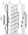
- FIG. 7An example of an allocation plan for the thirty-two WDM channels operated upon by the comb splitting system 40 is shown at reference numeral 61 in Fig. 7. Also shown in Fig. 7 at respective reference numerals 62, 63 are the ideal DWDM passbands of the first stage WDM/PS mechanisms 16 and of one of the second stage WDM/PS mechanisms 22.
- the WDM bandis preferably around 1.5 ⁇ m and the PS band is preferably around 1.3 ⁇ m, but they can also be interchanged, or at other wavelengths.
- the channel spacingis about 400 GHz (wavelength of about 3.2 nm).
- the first stage WDM/PS mechanism 16(Fig.
- the second stage DWDMs 56(Fig. 6) have a passband spacing of about 8x400 GHz and FSR 32x400 GHz, and do not need passband flattening and feedback control. Because of the large passband spacing and small number of splits for the second stage DWDM 56, a Fourier transform based waveguide filter (FF) is preferably used, instead of a WGR.
- FFFourier transform based waveguide filter
- the 32 channelsoccupy a total bandwidth of approximately one hundred nm from 1.48 ⁇ m to 1.58 ⁇ m.
- the wavelengths outside this wavelength rangenamely from 1.43 ⁇ m to 1.88 ⁇ m and from 1.58 ⁇ m to 1.63 ⁇ m, can optionally be used to deliver one more channel to each LU or used for testing purposes.
- a simple CWDMe.g. , a well known Mach-Zehnder interferometer, can be used in each ONU to separate the two channels.
- the FSR of the second stage DWDMs 56(Fig. 6) can be increased to about 64x400 GHz, thereby blocking the testing signal from reaching the ONU.
- Fig. 8shows at reference numeral 71 the power spectrum at the input of the first stage WDM/PS mechanism 16 when all of the thirty-two channels and one test channel are active but uncorrelated, with the same power levels.
- Fig. 8further shows the spectrum of the first and second stage outputs 18, 24 (Fig. 4) at reference numerals 72, 73, respectively.
- the broken line region 65represents the ideal passband of the first stage WDM/PS mechanism 16 (Fig. 4)
- the broken line region 66represents the ideal passband of the second stage WDM/PS mechanism 22 (Fig. 4).
- the crosstalk signal from the first stage(of relative magnitude ⁇ 1 ) is reduced by a factor ⁇ 2 in the second stage, except for channels adjacent to the pass channels.
- the channels at the edges of the passband of the second stage WDMhave a crosstalk reduction of - 0.5.
- the crosstalk signalsare channels 8 and 10 of relative magnitude ⁇ 1 , channels 7 and 11 of relative magnitude ⁇ 1 /2, channels 1, 17, 25, and the test channel of relative magnitude ⁇ 2 , and channels 2-6, 12-16, 18-24, and 26-32 of relative magnitude ⁇ 1 ⁇ 2 .
- the accumulated crosstalkis therefore 3 ⁇ 1 +4 ⁇ 2 +24 ⁇ 1 ⁇ 2 .
- Realistic crosstalk levels achievable with our current waveguide technologyare ⁇ 1 ⁇ 0.005 and ⁇ 2 ⁇ 0.0025 ( i . e . -23 and -26 db), and the accumulated crosstalk is ⁇ 0.025 or -16 dB.
- the accumulated crosstalk levelwould be 31 ⁇ 1 ⁇ 0.15 (-7.5 dB), and therefore the multistage comb splitting scheme offers an effective crosstalk reduction, which is an important factor that makes it practical. If sixty-four channels are active, an accumulated crosstalk would degrade by three dB, but it is still below the required crosstalk level for digital video transmission.
Landscapes
- Engineering & Computer Science (AREA)
- Computer Networks & Wireless Communication (AREA)
- Signal Processing (AREA)
- Optical Communication System (AREA)
- Optical Integrated Circuits (AREA)
Description
- The present invention generally relates to optical fiber communication networks, and more particularly, to a comb splitting system and method for a multichannel optical fiber communication network for multiplexing and/or demultiplexing an optical signal having a plurality of individual channels at various wavelengths.
- Recent research and development has focused on implementing optical communication networks to communicate information from central offices to individual living units (e.g., a subscriber's home) and from living units to the central offices. Several network approaches are possible, including for example, a point-to-point network, a power splitting network, or a wavelength division multiplexing network, as are further discussed hereafter.
- In a point-to-point network, one or more optical fibers directly link the central office to each living unit. This approach is perhaps the most straightforward and simplistic. However, it is apparent that even in the smallest network, this solution would involve an economically prohibitive number of interconnections, optical fibers, trenches, transmitters, and receivers.
- In a power splitting network, as is shown, for example, in US-A-4 483 582 of Sheem, a transmitter, receiver, and part of an optical fiber in the subscriber loop is shared by many living units using power splitters. The Sheem arrangement utilizes a first power splitter, a phase shifter, and a second power splitter in a first stage to produce equal power outputs of all of the frequencies introduced into the first power splitter, although shifted in phase. The equal power outputs are then applied to inputs of two power splitters in the second stage having, apparently, a wider bandpass characteristic than the first stage. A second phase shifter at the output of each of the two power splitters produces phase shifts which result in phase cancellations in third and fourth power splitters to produce single frequency outputs. A wide variety of power splitters are well known in the art. As an example, US-A-4 904 042 to Dragone describes a star coupler, which is a typical power splitter (PS). In a sense, a power splitter causes each signal to be broadcast over various fibers so that each living unit receives each signal. Although this network architecture is simple and low cost, it has large power penalties due to the power splitting, a small bandwidth due to the time sharing, poor subscriber privacy due to the broadcast distribution, and poor diagnostic and test capabilities in that individual subscriber lines cannot be adequately diagnosed and tested.
- A wavelength division multiplexing network employs wavelength division multiplexers (WDM). In this network, a particular channel (wavelength of carrier) is allocated to each living unit. Further, various channels are multiplexed over a single optical fiber and demultiplexed on individual fibers associated with each living unit utilizing WDMs, so that a virtual point-to-point connection between the central office and each living unit is achieved. WDMs, sometimes referred to as a filter or router, are well known in the art and are generally a device that can multiplex and/or demultiplex optical signal wavelengths. In general, a WDM is usually a passive optical network (PON) or device with multiple optical paths, each of which exhibits a particular passband, similar to an electrical signal processing filter. The passband permits passage of one or more particular wavelengths along the respective optical path, to the substantial exclusion of others. Thus, the WDM can be used to divide wavelengths (or channels) from a multichannel optical signal or to combine various wavelengths (or channels) on respective optical paths into one multichannel optical signal on one optical path. For an example of a WDM, see C. Dragoneet al., "Integrated Optics NxN Multiplexer on Silicon,"IEEE Photon. Technol. Lett., Vol. 3, p. 896 (1989), the disclosure of which is also set forth in U.S. Patent No. 5,136,671 to Dragone.
- A WDM network has less power loss in principal than the power splitting network and, furthermore, provides privacy in that each living unit only receives its respective channel. Although the WDM network offers a technically superior solution as compared to the power splitting network, the WDM network has historically required expensive, cost prohibitive components,i.e., the WDMs and wavelength-aligned transmitters and receivers. However, the recent development of less expensive key components makes the WDM network a more attractive approach. Examples of these key components include integrated WDMs, such as a waveguide grating router (WGR) as disclosed in C. Dragoneet al., "Integrated Optics NxN Multiplexer on Silicon,"IEEE Photon. Technol. Lett., Vol. 3, p. 896 (1989) (the disclosure of which is also set forth in U.S. Patent No. 5,136,671 to Dragone) and Fourier transform based waveguide filters (FF) as disclosed in pending U.S. patent application by Y.P. Li,et al., entitled "A Monolithic Optical Waveguide Filter Based On Fourier Expansion," with Serial No. 08/365,618 and filed December 28, 1994.
- A practical WDM network favors a two stage split of channels over a single stage split for the following reasons. On the one hand, a WDM network is economic when the number of splits is large. However, WGRs with large splitting ratios (e.g., 1x32) and good performance are expensive to fabricate. On the other hand, there are typically at least two natural splice nodes in a typical access network. A single fiber cable, housing many fibers, runs from the central office to a remote node (RN1) about three km away, and close to the center of a service area. These fibers are then split into smaller groups, each of which runs to another node, or pedestal (RN2), serving typically four to sixteen living units. The remote node (RN1) and pedestal (RN2) provide preexisting locations to install WDMs. By installing two stages of WDMs to increase the split ratio, the fiber count as well as the system cost can be reduced.
- In a band splitting multistage WDM network, the first stage makes a coarse split, and subsequent stages make finer and finer splits. In this scheme, the WDMs of the subsequent stages are largest in quantity, but are the most expensive to fabricate because they have the smallest channel spacing. Another disadvantage is that in order to maintain low loss for all channels, the WDMs in subsequent stages are required to have nearly flat passbands with sharp drop offs. Furthermore, the passbands of the subsequent stage WDMs should line up with the central office transmitters and receivers, which is difficult because the subsequent stage WDMs are installed at different locations and experience different temperature shifts of the transmission spectrum (i.e., usually about 0.012 nm/°C).
- Hence, a heretofore unaddressed need exists in the industry for a system and method for multiplexing and demultiplexing a plurality of optical signal channels at respective wavelengths using a multistage WDM network that can be implemented in two stages, if desired, and that does not suffer from the aforementioned problems and disadvantages.
- Briefly stated, the present invention provides for a comb splitting system and method for implementing a multistage WDM network. The comb splitting system and method can be utilized in a demultiplexing mode to demultiplex an optical signal having a plurality of multiplexed channels at various wavelengths into a plurality of individual channels and/or in a multiplexing mode to multiplex a plurality of channels at different wavelengths into a single optical signal.
- Structurally, the comb splitting system has at least two interconnected successive stages of WDMs. The system is described relative to two stages, but it should be understood that more than two may be implemented. A WDM of the first stage is interconnected with an optical path, for example, an optical fiber, waveguide, or other optical signal carrier that carries a multichannel optical signal having a plurality of individual channels at various wavelengths. The first stage WDM communicates bands of channels to respective WDMs of the second stage via suitable optical paths. Each of the bands has a plurality of the individual channels that are separated by at least one other of the channels. Each second stage WDM, which is allocated to a particular band, is interconnected to optical paths, each for carrying one or more individual channels. Furthermore, in accordance with a significant feature of the present invention, the bandpasses associated with the first stage WDM is narrower than the bandpasses associated with the second stage WDMs.
- The first and second stage WDMs can reside on a single integrated circuit, for example, an optical application specific integrated circuit (OASIC). They can also be situated within separate discrete electronic components that are connected locally at a node of an optical fiber network. Moreover, they can be remotely separated. For instance, they can be situated at different nodes of an optical fiber network and interconnected via a fiber cable so that a distribution network is formed.
- The operation of the comb splitting system is as follows. Because the operation of the comb splitting system in the multiplexing mode is generally analogous to the demultiplexing mode but in reverse order, only the operation in the demultiplexing mode is set forth hereafter for simplicity. The first stage WDM receives the multichannel optical signal having the plurality of individual channels at various wavelengths. The first stage WDM demultiplexes the optical signal into a plurality of bands by utilizing narrow bandpasses. Each of the bands has a plurality of the individual channels that are separated by at least one other of the channels. Furthermore, the second stage has a WDM allocated to each of the bands for demultiplexing the individual channels from each of the bands with wide bandpass filters that have a wider bandpass than the narrow bandpass filters associated with the first stage WDM.
- The novel method provided by the present invention can be broadly summarized as follows. In the demultiplexing mode, first, an optical signal having a plurality of individual channels at various wavelengths is received by a first stage WDM, and bands of individual channels are demultiplexed from the plurality by utilizing first bandpasses in the first stage WDM. The channels in each of the bands being separated by at least one other channel. Second, the bands are communicated to respective second stage WDMs and individual channels are demultiplexed from each of the bands by the second stage WDMs with bandpasses that are wider than the bandpasses of the first stage WDM.
- Similarly; but in reverse order, the novel method as applied to the multiplexing mode is as follows. First, a plurality of individual channels are multiplexed into bands via bandpasses associated with second stage WDMs. The channels in each of the bands are separated by at least one other channel. Second, the bands are multiplexed from the plurality to form a single multichannel signal by utilizing a first stage WDM and its associated bandpasses that are narrower than the bandpasses of the second stage WDMs.
- The present invention has numerous advantages, a few of which are delineated hereafter, as merely examples.
- An advantage of the comb splitting system is its cost effectiveness. Inexpensive WDMs can be utilized in the second and subsequent stages, while a more expensive WDM having narrower bandpasses is utilized in the first stage.
- Another advantage of the comb splitting system is that it effectively reduces accumulated crosstalk between channels. In fact, the inventors have determined that there is approximately 8 decibels (dB) of reduction in crosstalk in a 32 channel system.
- Another advantage of the comb splitting system is that it is substantially insensitive to temperature fluctuations, especially when implemented in a distribution network where the first and second stages reside at different physical node locations.
- Another advantage of the comb splitting system is that it permits testing of individual optical paths using, for example, optical time domain reflectometry (OTDR).
- Another advantage of the comb splitting system is that it is simple in structure, easy to implement and fabricate on a mass scale, and reliable in operation.
- Another advantage of the comb splitting system is that it can be implemented on a single integrated circuit (IC) or in stages of ICs.
- Another advantage of the comb splitting system is that it can be implemented with completely passive elements to created a PON.
- Another advantage of the comb splitting system is that it can be implemented with a device having both a WDM and a power splitting mechanism. An example of such a device is described in U.S. Patent No. 5,285,305 to Cohenet al.
- Other features and advantages of the present invention will become apparent to one with skill in the art upon examination of the following drawings and detailed description. It is intended that all such additional features and advantages be included herein within the scope of the present invention, as is defined in the appended claims.
- The present invention can be better understood with reference to the following drawings. The drawings are not necessarily to scale, emphasis instead being placed upon clearly illustrating principles of the present invention. Moreover, like reference numerals designate corresponding parts throughout the several views.
- Fig. 1 is a block diagram illustrating the comb splitting system and method of the present invention wherein the system has one 1xM (1 optical path in/out; M optical paths out/in) WDM in the first stage, M 1xN WDMs in the second stage, and NM channels;
- Fig. 2 is a block diagram illustrating a first embodiment of the comb splitting system of Fig. 1 wherein the first embodiment has two stages, one 1x2 WDM in the first stage, two 1x2 WDMs in the second stage, and four channels;
- Fig. 3 is a graph illustrating channel passbands in the specific comb splitting system of Fig. 2;
- Fig. 4 is a block diagram of a second embodiment of the comb splitting system of Fig. 1 wherein the second embodiment has two stages, a 1x8 WDM/PS mechanism in the first stage, eight 1x4 WDM/PS mechanisms in the second stage, 32 WDM channels, and 32 PS channels;
- Fig. 5 is a block diagram illustrating the WDM/PS mechanism in the first stage of Fig. 4;
- Fig. 6 is a block diagram illustrating the WDM/PS mechanism in the second stage of Fig. 4;
- Fig. 7 is a graph illustrating channel passbands in the specific comb splitting system of Fig. 4; and
- Fig. 8 is a graph illustrating channel separation, filtering, and crosstalk along the wavelength spectrum in the specific comb splitting system of Fig. 4.
- The generalized comb splitting system in accordance with the present invention is illustrated in Fig. 1 and is denoted by the
reference numeral 10. Thecomb splitting system 10 has at least two interconnectedsuccessive stages first stage 12 has a1xM WDM 16 with an input/outputoptical path 17 for carrying the optical signal having NM channels and M output/inputoptical paths 18. TheWDM 16 demultiplexes and/or multiplexes the optical signal onoptical path 17 into/from M bands by utilizing narrow bandpasses. Each of the M bands has a plurality of individual channels that are separated by at least one other of the channels. In the preferred embodiment, the bands are defined as follows. A first band withchannels 1, M+1, 2M+1..., (N-1) M+1 is carried on branch B1. A second band withchannels 2, M+2, 2M+2..., (N-1) M+2 is communicated on branch B2. The foregoing pattern continues until reaching the Mth branch BM with channels M, 2M, 3M,..., NM. - The
second stage 14 has Mparallel 1xN WDMs 22. Each of theWDMs 22 is configured to communicate a respective one of the M bands on a respectiveoptical path 18. EachWDM 22 demultiplexes and/or multiplexes individual channels from its corresponding band. In the preferred embodiment, theM WDMs 22 demultiplex and/or multiplex the individual channels as follows: 1, M+1,..., (N-1) M+1; 2, M+2, ..., (N-1) M+2; and M, 2M, ..., NM. - Note that the
comb splitting system 10 of Fig. 1 can be periodic with a periodicity N1N2Δ, where N1 is the first stage split ratio and where N2 is the second stage split ratio. Along these lines, a wavelength λ' located N1N2Δ away from λ1 goes to the same output as λ1. Thus, thesystem 10 can be constructed with more than two stages, if desired. For example, the 1xMfirst stage WDM 16 can be implemented as theentire IxNM system 10 as shown in Fig. 1, so that M is changed to NM and a three stage 1xN2M system 10 is formed. - The
WDMs WDMs - The
optical paths - The
comb splitting system 10 can be physically implemented in several different ways. TheWDMs comb splitting system 10 can reside on a single integrated circuit, for example, an optical application specific integrated circuit (OASIC). With this configuration, theoptical paths 18 can be integrated circuit optical waveguides. They can also be situated within separate discrete electronic components that are connected locally at a node (e.g., RN1, RN2) of an optical fiber network. Moreover, they can be remotely separated. For instance, they can be situated at different nodes (e.g., RN1, RN2) of an optical fiber network and interconnected via a fiber cable(s) 18 or waveguide(s) 18 so that a distribution network is formed. - In accordance with a significant feature of the present invention, the
second stage WDMs 22 are configured to utilize bandpasses that are wider than the bandpasses utilized by thefirst stage WDM 16, and the periodicity (i.e., the free spectral range, FSR) of channels at thesecond stage WDMs 22 is larger than at thefirst stage WDMs 16. - As a result of the foregoing configuration, the
system 10 has numerous advantages, a few of which are delineated hereafter. First, thesecond stage WDMs 22 are less expensive and physically smaller than thefirst stage WDM 16. Second, the separation and routing of channels in thesystem 10 reduces crosstalk between the channels, or interference caused by coupling of channels. Specifically, in the demultiplexing mode, any crosstalk resulting from thefirst stage 12 is cleaned up by thesecond stage 14, and in the multiplexing mode, any crosstalk resulting from thesecond stage 14 is cleaned upon in thefirst stage 12. Third, the synchronization of the WDM passbands with the wavelengths of the transmitters/receivers in the central office is also much easier because only thefirst stage WDM 12, which is at a single location (RN 1) close to the central office, needs to be synchronized. Fourth, because of their much wider passbands and FSR, the WDMs at later stages can tolerate larger fabrication errors, do not require flat passbands and birefringence compensation, and can tolerate full environmental temperature variations without feedback control in the central office. These and other advantages will become more apparent in later discussions pertaining to specific implementations. - Fig. 2 illustrates a
first embodiment 30 of the generalizedcomb splitting system 10 of Fig. 1 and is meant to be a nonlimiting example, and Fig. 3 graphically illustrates the passbands associated with the first andsecond stage WDMs comb splitting system 30 is a 1x4 device, having a1x2 WDM 12 in itsfirst stage 12 and two1x2 WDMs second stage 14. - The
first stage WDM 16 communicates with an optical signal onoptical path 17 having four channels λ1, λ2, λ3, λ4, which are preferably equally spaced in frequency as shown atreference numeral 31 in Fig. 3 with the spacing Δ of, for example but not limited to, Δ=400 gigahertz (GHz). Thefirst stage WDM 16 has channel spacing equal to Δ and a periodicity (i.e., the free spectral range, FSR) MΔ, where M=2 is the first stage split ratio. Thus, in the demultiplexing mode, thefirst stage WDM 16 divides the four channels into two combs, with λ1λ3 in one output and λ2λ4 in the other, as is further illustrated in Fig. 3 atreference numeral 32. - The
second stage WDMs second stage WDM 22b is shifted by Δ relative to that ofsecond stage WDM 22a, so that the centers of passbands of bothWDMs 22 always line up with the input channels λ1 through λ4, as illustrated atreference numerals second stage WDMs 22 thus further split the combs from thefirst stage WDM 16 into separate channels. - A second embodiment of the
comb splitting system 10 of Fig. 1 is illustrated in Fig. 4 and generally denoted byreference numeral 40. Thecomb splitting system 40 is a 1 x32 device for demultiplexing a multichannel signal into 32 WDM channels and 32 PS signals. In structure, thecomb splitting system 40 has afirst stage 12 with a single 1x8 combined WDM/PS mechanism 16 interconnected with asecond stage 14 having eight 1x8 WDM/PS mechanisms 22. In essence, each of the combined WDM/PS mechanisms - For purposes of discussion, hereafter, a "coarse WDM" (or "CWDM") is a WDM having a wider bandpass and larger FSR than another WDM (i.e., "dense WDM"), and a "dense WDM" (or "DWDM") is a WDM having a narrower bandpass and smaller FSR than another WDM (i.e., "coarse WDM"). Moreover, the coarse WDM (or CWDM) is used to separate or combine the PS band and the WDM band.
- It is advantageous to include a PS with a WDM for at least the following reasons. First, some distribution schemes,e.g., broadcasting cable television (TV) signals using high powered linearized optical fiber amplifiers (LOFA) requires power splitters. Second, it would be more economically viable to initially employ PSs in inexpensive low speed non-wavelength-selective transmitters and receivers when the bandwidth requirement is small, and upgrade the system to a fully WDM network when the bandwidth requirement becomes large. A suitable WDM/
PS mechanism - The
comb splitting system 40 is used as a demultiplexer as follows. A coarse WDM (not shown) combines a PS signal and the WDM channels at the central office and forwards the combined optical signal to the first stage WDM/PS mechanism 16 viaoptical path 17, as shown in Fig. 4. Preferably, the first stage WDM/PS mechanism 16 is housed in the first remote node (RN1) located near the center of a service area of typically up to about 480 LUs. EachRN 1 serves up to 480 LUs, and therefore, there are typically fifteen WDM/PS mechanisms 16 in a single RN1 enclosure, with a single-sheath (bundle) multi-fiber cable running from the CO to RN1. Each of the eight RN1 outputs serves a separate pedestal (RN2), which host a second stage WDM/PS mechanism 22 serving four LUs. - Fig. 5 illustrates further details of the preferred embodiment of the WDM/PS mechanism 16 (Fig. 4). With reference to Fig. 5, the WDM/
PS mechanism 16 has aCWDM 42 at its input. TheCWDM 42 splits the two wavelength bands and feeds them into a1x4 DWDM 44 and a1x4 PS 46, respectively. Each output of theDWDM 44 is subsequently combined with an output of thePS 46, using anotherCWDM 48 that has the same spectral response as theCWDM 42. Thus, for one wavelength band (referred to as the WDM band), the WDM/PS mechanism 16 functions as a WDM, and for the other wavelength band (the PS band), the WDM/PS mechanism 16 functions transparently as a PS. If both wavelength bands are present at the inputoptical path 17, each outputoptical path 24 gets 1/8 of the power of the PS band and a wavelength channel of the WDM band. Extra ports 52 can be added for diagnostic purposes. For example, a 2x5 DWDM and a 2x5 PS can be used instead of 1x4's, with the extra output having a fraction (e.g. 1/10) of the power of the regular outputs, thus providing direct local access to the PS and WDM signals.- Fig. 6 illustrates further details of the preferred embodiment of the WDM/PS mechanism 22 (Fig. 4). Each WDM/
PS mechanism 22 comprises aCWDM 54 interconnected with aDWDM 56 viaoptical path 55 and aPS 58 viaoptical path 57. TheDWDM 56 receives a collection of four WDM signals onoptical path 55 and filters and separates these channels to provide a restrictive channel on eachoptical path 24. Furthermore, thePS 58 receives a collection of four broadcast signals onoptical path 57 and filters and separates the broadcast signals to provide a respective broadcast signal on each of fouroptical paths 24. - In some cases,e.g., in an optical network unit (ONU) where the WDM/
PS mechanism 22 of Fig. 6 are fed to separate detectors for the PS and WDM bands, the CWDMs 42 (Fig. 5) are not needed. - An example of an allocation plan for the thirty-two WDM channels operated upon by the
comb splitting system 40 is shown atreference numeral 61 in Fig. 7. Also shown in Fig. 7 atrespective reference numerals PS mechanisms 16 and of one of the second stage WDM/PS mechanisms 22. The WDM band is preferably around 1.5 µm and the PS band is preferably around 1.3 µm, but they can also be interchanged, or at other wavelengths. The channel spacing is about 400 GHz (wavelength of about 3.2 nm). The first stage WDM/PS mechanism 16 (Fig. 4) has a passband spacing of about 400 GHz and FSR of about 8x400 GHz, and needs no birefringence correction and only a small degree of passband flattening. The second stage DWDMs 56 (Fig. 6) have a passband spacing of about 8x400 GHz and FSR 32x400 GHz, and do not need passband flattening and feedback control. Because of the large passband spacing and small number of splits for thesecond stage DWDM 56, a Fourier transform based waveguide filter (FF) is preferably used, instead of a WGR. - The 32 channels occupy a total bandwidth of approximately one hundred nm from 1.48 µm to 1.58 µm. The wavelengths outside this wavelength range, namely from 1.43 µm to 1.88 µm and from 1.58 µm to 1.63 µm, can optionally be used to deliver one more channel to each LU or used for testing purposes. If two channels are delivered to each LU, a simple CWDM,e.g., a well known Mach-Zehnder interferometer, can be used in each ONU to separate the two channels. If the extra channels are used for testing, the FSR of the second stage DWDMs 56 (Fig. 6) can be increased to about 64x400 GHz, thereby blocking the testing signal from reaching the ONU.
- The comb splitting system 40 (Fig. 4) significantly diminishes crosstalk between channels. In this regard, Fig. 8 shows at reference numeral 71 the power spectrum at the input of the first stage WDM/
PS mechanism 16 when all of the thirty-two channels and one test channel are active but uncorrelated, with the same power levels. Fig. 8 further shows the spectrum of the first and second stage outputs 18, 24 (Fig. 4) atreference numerals broken line region 65 represents the ideal passband of the first stage WDM/PS mechanism 16 (Fig. 4), and thebroken line region 66 represents the ideal passband of the second stage WDM/PS mechanism 22 (Fig. 4). - When two stages of WDMs, with crosstalk levels of δ1 and δ2, respectively, are cascaded in the
comb splitting system 40, the crosstalk signal from the first stage (of relative magnitude δ1) is reduced by a factor δ2 in the second stage, except for channels adjacent to the pass channels. The channels at the edges of the passband of the second stage WDM have a crosstalk reduction of - 0.5. Thus, in the final output that passes channel 9, the crosstalk signals arechannels 8 and 10 of relative magnitude δ1, channels 7 and 11 of relative magnitude δ1/2,channels - It will be obvious to those skilled in the art that many modifications and variations may be made to the embodiments as described without substantially departing from the scope of the present invention as set forth in the appended claims.
Claims (21)
- A comb splitting system (10) for demultiplexing an optical signal into a plurality of individual channels at various wavelengths, comprising:a first stage wavelength division demultiplexer (16) for receiving said optical signal having said plurality of individual channels at various wavelengths and for simultaneously demultiplexing said plurality into bands by utilizing first bandpasses, each of said bands having a plurality of said individual channels that are separated from each other; anda plurality of second stage wavelength division demultiplexers for simultaneously demultiplexing said individual channels from each of said bands with second bandpasses;wherein the individual channels in each band are separated from each other by at least one other channel; and
wherein said second bandpasses are wider than said first bandpasses;
CHARACTERIZED IN THAT:at least one of said first and second stage wavelength division demultiplexers each further comprise a Dragone router. - The system of claim 1, wherein there are NM of said individual channels and M second stage wavelength division demultiplexers, each Ith wavelength division demultiplexer of said M second stage wavelength division demultiplexers receiving and demultiplexing a channel I and a channel M+I of said NM channels.
- The system of claim 2, wherein N is 2 and M is 2.
- The system of claim 2, wherein N is 4 and M is 8.
- The system of any of the preceding claims, further comprising optical fibers configured to transfer said bands from said first stage wavelength division demultiplexer to said second stage wavelength division demultiplexers.
- The system of any of claims 1 to 4, further comprising waveguides configured to transfer said bands from said first stage wavelength division demultiplexer to said second stage wavelength division demultiplexers.
- The system (40) of any of the preceding claims, wherein the optical signal contains multiplexed the WDM channels and a plurality of power splitting signals;
CHARACTERIZED IN THAT:a power splitter is associated with each said second stage WDM (22a, 22b), said power splitters configured to collectively demultiplex the plurality of power channels that are multiplexed on said optical signal. - A comb splitting system for multiplexing a plurality of individual channels at various wavelengths into an optical signal, comprising:a plurality of first stage wavelength division multiplexers (22a, 22b) for producing bands by simultaneously multiplexing said individual channels with first bandpasses, each of said bands having a plurality of said individual channels that are separated from each other; anda second stage wavelength division multiplexer (16) for providing said optical signal having said plurality of individual channels at various wavelengths by simultaneously multiplexing said bands by utilizing second bandpasses;wherein said channels in said bands are separated by at least one other of said channels; and
wherein said second bandpasses are narrower than said first bandpasses;
CHARACTERIZED IN THAT:at least one of said first and second stage wavelength division multiplexers each further comprise a Dragone router. - The system of claim 8, wherein there are NM of said individual channels and M second stage wavelength division multiplexers, each Ith wavelength division multiplexer of said M second stage wavelength division multiplexers multiplexing a channel I and a channel M+I of said NM channels.
- The system of claim 9, wherein N is 2 and M is 2.
- The system of claim 9, wherein N is 4 and M is 8.
- The system of any of claims 8 to 11, further comprising optical fibers configured to transfer said bands from said first stage wavelength division multiplexer to said second stage wavelength division multiplexers.
- The system of any of claims 8 to 11, further comprising waveguides configured to transfer said bands from said second stage wavelength division multiplexers to said first stage wavelength division multiplexer.
- The system of any of claims 8 to 13, further comprising a power splitter associated with each said first stage wavelength division multiplexer, said power splitters configured to collectively multiplex a plurality of power signals that are multiplexed on said optical signal.
- The system of any of the preceding claims, wherein said first and second stage wavelength division multiplexers reside on a single integrated circuit.
- The system of any of claims 1 to 14, wherein said first and second stage wavelength division multiplexers reside within separate discrete electronic components that are connected locally at a node of an optical fiber network.
- The system of any of claims 1 to 14, wherein said first and second stage wavelength division multiplexers are separated and reside at different nodes of an optical fiber network and are interconnected via a fiber cable so that a distribution network is formed.
- The system of any of the preceding claims, wherein said spaced channels are separated from each other by approximately equally spaced wavelength channels along a frequency spectrum.
- The system of any of the preceding claims, wherein said first and second stage wavelength division multiplexers are passive elements.
- The system of any of claims 1 to 18, wherein at least one of said first and second stage wavelength division multiplexers comprises a Fourier filter.
- The system of any of claims 1 to 18, wherein said first and second stages are passive networks.
Applications Claiming Priority (2)
| Application Number | Priority Date | Filing Date | Title |
|---|---|---|---|
| US525938 | 1990-05-16 | ||
| US08/525,938US5680490A (en) | 1995-09-08 | 1995-09-08 | Comb splitting system and method for a multichannel optical fiber communication network |
Publications (3)
| Publication Number | Publication Date |
|---|---|
| EP0762690A2 EP0762690A2 (en) | 1997-03-12 |
| EP0762690A3 EP0762690A3 (en) | 1999-05-12 |
| EP0762690B1true EP0762690B1 (en) | 2006-07-12 |
Family
ID=24095242
Family Applications (1)
| Application Number | Title | Priority Date | Filing Date |
|---|---|---|---|
| EP96306219AExpired - LifetimeEP0762690B1 (en) | 1995-09-08 | 1996-08-28 | Comb splitting system for a multichannel optical fiber communication network |
Country Status (6)
| Country | Link |
|---|---|
| US (1) | US5680490A (en) |
| EP (1) | EP0762690B1 (en) |
| JP (1) | JPH09105833A (en) |
| AU (1) | AU703880B2 (en) |
| CA (1) | CA2179843C (en) |
| DE (1) | DE69636334T2 (en) |
Cited By (1)
| Publication number | Priority date | Publication date | Assignee | Title |
|---|---|---|---|---|
| US11621784B1 (en) | 2021-09-29 | 2023-04-04 | X Development Llc | Photonic integrated circuit with optical deinterleaver |
Families Citing this family (86)
| Publication number | Priority date | Publication date | Assignee | Title |
|---|---|---|---|---|
| US5852505A (en)* | 1994-12-28 | 1998-12-22 | Lucent Technologies Inc. | Dense waveguide division multiplexers implemented using a first stage fourier filter |
| US5864413A (en)* | 1996-02-23 | 1999-01-26 | Lucent Technologies, Inc. | Passive optical network for dense WDM downstream data transmission and upstream data transmission |
| US6005697A (en) | 1996-07-23 | 1999-12-21 | Macro-Vision Communications, L.L.C. | Multi-wavelength cross-connect optical network |
| US5867291A (en) | 1996-10-29 | 1999-02-02 | Chorum Technologies Inc. | Programmable wavelength router |
| IT1283372B1 (en)* | 1996-07-31 | 1998-04-17 | Pirelli Cavi S P A Ora Pirelli | DEVICE FOR THE INSERTION AND EXTRACTION OF OPTICAL SIGNALS |
| US6285478B1 (en) | 1998-03-26 | 2001-09-04 | Chorum Technologies Lp | Programmable optical add/drop device |
| US6208444B1 (en) | 1996-10-29 | 2001-03-27 | Chorum Technologies Inc. | Apparatus for wavelength demultiplexing using a multi-cavity etalon |
| US6498680B1 (en) | 1996-10-29 | 2002-12-24 | Chorum Technologies Lp | Compact tunable optical wavelength interleaver |
| US6208442B1 (en) | 1998-03-26 | 2001-03-27 | Chorum Technologies, Inc. | Programmable optical multiplexer |
| US6545783B1 (en) | 1996-10-29 | 2003-04-08 | Chorum Technologies Lp | Optical wavelength add/drop multiplexer |
| US6847786B2 (en) | 1996-10-29 | 2005-01-25 | Ec-Optics Technology, Inc. | Compact wavelength filter using optical birefringence and reflective elements |
| US6166838A (en)* | 1997-03-24 | 2000-12-26 | Chorum Technologies, Inc. | Optical add/drop wavelength switch |
| US6115155A (en) | 1996-10-29 | 2000-09-05 | Chorum Technologies Inc. | System for dealing with faults in an optical link |
| US6163393A (en)* | 1996-10-29 | 2000-12-19 | Chorum Technologies Inc. | Method and apparatus for wavelength multipexing/demultiplexing |
| US6243200B1 (en) | 2000-03-02 | 2001-06-05 | Chorum Technologies, Inc. | Optical wavelength router based on polarization interferometer |
| US6519022B1 (en) | 1997-04-02 | 2003-02-11 | Chorum Technologies Lp | Optical routing switch using symmetric liquid crystal cells |
| US6631018B1 (en) | 1997-08-27 | 2003-10-07 | Nortel Networks Limited | WDM optical network with passive pass-through at each node |
| US6141076A (en)* | 1997-11-28 | 2000-10-31 | Chorum Technologies, Inc. | Spatial light modulators constructed from ferroelectric liquid crystal devices with twisted structure |
| US6094246A (en) | 1998-01-06 | 2000-07-25 | Chorum Technologies | Acute twist nematic liquid crystal electro-optic modulator for use in an infrared optical communication system having extinction ratio of -25db |
| JPH11234217A (en)* | 1998-02-10 | 1999-08-27 | Alps Electric Co Ltd | WDM optical communication equipment |
| IL124639A (en) | 1998-05-25 | 2001-09-13 | Handelman Doron | Optical communication method and system using wavelength division multiplexing |
| US6388782B1 (en) | 1998-06-01 | 2002-05-14 | Sarnoff Corporation | Multi-wavelength dense wavelength division multiplexed optical switching systems |
| US6014237A (en)* | 1998-06-01 | 2000-01-11 | Sarnoff Corporation | Multiwavelength mode-locked dense wavelength division multiplexed optical communication systems |
| JP3098235B2 (en)* | 1998-08-04 | 2000-10-16 | 日本電信電話株式会社 | Wavelength demultiplexer, optical spectrum analyzer and optical bandpass filter |
| US6263126B1 (en) | 1998-08-06 | 2001-07-17 | Avanex Corporation | Fiber optic dense wavelength division multiplexer utilizing a multi-stage parallel cascade method of wavelength separation |
| US6134358A (en) | 1998-08-27 | 2000-10-17 | Chorum Technologies Inc. | N x N switch array with reduced components |
| US6782203B2 (en)* | 1998-08-31 | 2004-08-24 | Lucent Technologies Inc. | Scalable optical demultiplexing arrangement for wide band dense wavelength division multiplexed systems |
| US6192058B1 (en) | 1998-09-18 | 2001-02-20 | Sarnoff Corporation | Multiwavelength actively mode-locked external cavity semiconductor laser |
| US6556742B2 (en)* | 1998-11-04 | 2003-04-29 | Fujitsu Limited | Optical wavelength division multiplexed system using wavelength splitters |
| US6721508B1 (en) | 1998-12-14 | 2004-04-13 | Tellabs Operations Inc. | Optical line terminal arrangement, apparatus and methods |
| US6208780B1 (en) | 1999-01-19 | 2001-03-27 | Lucent Technologies Inc. | System and method for optical monitoring |
| US6160932A (en)* | 1999-02-16 | 2000-12-12 | Wavesplitter Technologies, Inc. | Expandable wavelength division multiplexer based on interferometric devices |
| IL129031A (en) | 1999-03-17 | 2003-02-12 | Handelman Doron | Network control system for optical communication networks |
| US6181849B1 (en) | 1999-04-30 | 2001-01-30 | Lucent Technologies, Inc. | Interleaved wavelengths multi/demultiplexer with multiple-input-ports and multiple-output-ports for wavelength add/drop WDM systems |
| US20060165413A1 (en)* | 1999-05-24 | 2006-07-27 | Broadband Royalty Corporation | DWDM CATV return system with up-converters to prevent fiber crosstalk |
| US6519060B1 (en)* | 1999-06-04 | 2003-02-11 | Chorum Technologies Lp | Synchronous optical network in frequency domain |
| US6160665A (en)* | 1999-06-04 | 2000-12-12 | Chorum Technologies Inc. | High extinction ratio polarization beamsplitter |
| US6486984B1 (en)* | 1999-06-07 | 2002-11-26 | Agilent Technologies, Inc. | Wavelength monitor using hybrid approach |
| WO2000077957A1 (en)* | 1999-06-15 | 2000-12-21 | Mitsubishi Denki Kabushiki Kaisha | Dispersion compensating device and dispersion compensating system |
| US6452681B1 (en) | 1999-06-22 | 2002-09-17 | Fitel Usa Corp | Optical spectrum analyzer |
| JP4498509B2 (en) | 1999-11-16 | 2010-07-07 | 富士通株式会社 | Control device and control method of wavelength division multiplexing optical amplifier |
| US6396609B1 (en) | 1999-12-20 | 2002-05-28 | Chorum Technologies, Lp | Dispersion compensation for optical systems |
| KR20010061613A (en)* | 1999-12-28 | 2001-07-07 | 윤종용 | Node structure of wavelength division multiplexing system for modular upgradabilty |
| WO2001050662A1 (en)* | 1999-12-29 | 2001-07-12 | Koninklijke Philips Electronics N.V. | Dwdm catv return system with up-converters to prevent fiber crosstalk |
| US6351583B1 (en) | 2000-01-28 | 2002-02-26 | Agere Systems Guardian Corp. | Multiple laser wavelength stabilization |
| JP3651876B2 (en)* | 2000-02-07 | 2005-05-25 | エヌティティエレクトロニクス株式会社 | Wavelength multiplexed optical signal multiplexing / demultiplexing method |
| US6559992B2 (en) | 2000-03-27 | 2003-05-06 | Chorum Technologies Lp | Adjustable chromatic dispersion compensation |
| US6697574B2 (en)* | 2000-03-31 | 2004-02-24 | At&T Corp. | Multiple input waveguide grating router for broadcast and multicast services |
| US6426816B1 (en) | 2000-05-01 | 2002-07-30 | Chorum Technologies, Lp | Wide transmission optical comb filter with wide pass band and wide stop band |
| US6529649B1 (en)* | 2000-05-01 | 2003-03-04 | Lucent Technologies Inc. | Optical filter with improved crosstalk rejection |
| US6763191B1 (en)* | 2000-07-25 | 2004-07-13 | Eci Telecom Ltd. | Optical switching apparatus and methods |
| US6459487B1 (en) | 2000-09-05 | 2002-10-01 | Gang Paul Chen | System and method for fabricating components of precise optical path length |
| FR2818059B1 (en)* | 2000-12-07 | 2003-02-07 | Cit Alcatel | DEVICE FOR DEMULTIPLEXING FREQUENCY BANDS |
| WO2002054642A2 (en)* | 2000-12-29 | 2002-07-11 | Luxcore Networks, Inc. | High density reconfigurable optical multiplexer |
| US7330659B2 (en)* | 2001-03-02 | 2008-02-12 | Lucent Technologies Inc. | Wavelength filter that operates on sets of wavelength channels |
| US6574396B1 (en)* | 2001-03-12 | 2003-06-03 | Lucent Technologies Inc. | Waveguide grating arrangement using a segmented reflector |
| FR2822949B1 (en)* | 2001-03-27 | 2004-01-09 | Commissariat Energie Atomique | INTEGRATED OPTICAL SPECTROMETER WITH HIGH SPECTRAL RESOLUTION, IN PARTICULAR FOR HIGH-FREQUENCY TELECOMMUNICATIONS AND METROLOGY, AND METHOD OF MANUFACTURE |
| US6754413B2 (en)* | 2001-04-23 | 2004-06-22 | Tropic Networks Inc. | Optical multiplexer, demultiplexer and methods |
| US6912340B2 (en)* | 2001-04-23 | 2005-06-28 | Tropic Networks Inc | Optical ring interconnect |
| SE524863C2 (en)* | 2001-04-23 | 2004-10-12 | Transmode Systems Ab | Optical coarse wavelength division multiplexing system has multiple logical optical rings that form multiplexed ring structure, such that each ring links several nodes of ring structure |
| US6515786B1 (en) | 2001-08-03 | 2003-02-04 | Chorum Technologies Lp | Bandwidth variable wavelength router and method of operation |
| US7162155B2 (en)* | 2001-09-04 | 2007-01-09 | Doron Handelman | Optical packet switching apparatus and methods |
| US7106967B2 (en)* | 2001-09-04 | 2006-09-12 | Doron Handelman | Optical packet switching apparatus and methods |
| FR2830709B1 (en)* | 2001-10-05 | 2004-01-30 | Cit Alcatel | SELECTIVE FREQUENCY SWITCHING DEVICE AND RECONFIGURABLE OPTICAL DELAY CIRCUIT INCORPORATED |
| US20030081888A1 (en)* | 2001-11-01 | 2003-05-01 | Doerr Christopher Richard | Integrated wavelength router |
| JP3709925B2 (en)* | 2001-11-09 | 2005-10-26 | 日立電線株式会社 | Waveguide type optical multiplexer / demultiplexer |
| KR100431195B1 (en)* | 2001-12-18 | 2004-05-12 | 한국전자통신연구원 | A multi wavelength locking method and apparatus by using acousto-optic tunable filter |
| JP4161808B2 (en) | 2002-08-21 | 2008-10-08 | 住友電気工業株式会社 | Optical transmission system |
| JP4259186B2 (en) | 2002-08-29 | 2009-04-30 | 住友電気工業株式会社 | Optical transmission system |
| DE10300934B4 (en)* | 2003-01-13 | 2012-04-12 | Adva Ag Optical Networking | Optical filter arrangement for an optical wavelength division multiplex transmission system |
| WO2004114555A1 (en) | 2003-06-18 | 2004-12-29 | Nippon Telegraph And Telephone Corporation | Optical wavelength multiplex access system and optical network unit |
| US7167620B2 (en)* | 2003-07-16 | 2007-01-23 | Doron Handelman | Devices and methods for all-optical processing and storage |
| KR100658338B1 (en)* | 2004-04-09 | 2006-12-14 | 노베라옵틱스코리아 주식회사 | Wavelength Division Multiplexing Passive Fluorescent Network with Multistage Branch Light Distribution Network |
| JP4541053B2 (en)* | 2004-07-08 | 2010-09-08 | 日本電信電話株式会社 | Optical transmission system |
| KR100661348B1 (en)* | 2004-11-03 | 2006-12-27 | 삼성전자주식회사 | Apparatus and Method for Label Transmission in Optical Packet Data Switching Network |
| US7570844B2 (en)* | 2005-01-18 | 2009-08-04 | Doron Handelman | Photonic integrated circuit device and elements thereof |
| US7366365B2 (en)* | 2005-11-23 | 2008-04-29 | Princeton Lightwave, Inc. | Tissue scanning apparatus and method |
| US20080142285A1 (en)* | 2006-12-18 | 2008-06-19 | Caterpillar Inc. | Airflow redirector |
| EP2182659B1 (en)* | 2008-10-30 | 2019-04-17 | ADTRAN GmbH | Method and optical system for the transmission of signals |
| US8285144B2 (en)* | 2009-07-30 | 2012-10-09 | Jds Uniphase Corporation | Optical device for rearranging wavelength channels |
| US9319169B2 (en)* | 2010-07-07 | 2016-04-19 | Tyco Electronics Subsea Communications Llc | Orthogonally-combining interleaving filter multiplexer and systems and methods using same |
| KR101285766B1 (en)* | 2012-05-18 | 2013-07-19 | 에스케이텔레콤 주식회사 | Bidirectional optical transmitting/receiving module |
| US10411812B1 (en)* | 2013-03-15 | 2019-09-10 | Forrest Rose | Optical interconnect computing module tolerant to changes in position and orientation |
| US20160164625A1 (en)* | 2013-07-16 | 2016-06-09 | Commscope Technologies Llc | Distributed wave division multiplexing systems |
| US9329345B2 (en)* | 2013-11-22 | 2016-05-03 | Alcatel Lucent | Hybrid wavelength selective switch |
| US10819431B2 (en)* | 2016-06-08 | 2020-10-27 | Fraunhofer-Gesellschaft zur Förderung der angewandten Forschung e.V. | Optical communication system and method |
Family Cites Families (17)
| Publication number | Priority date | Publication date | Assignee | Title |
|---|---|---|---|---|
| US4483582A (en)* | 1980-04-23 | 1984-11-20 | The United States Of America As Represented By The Secretary Of The Navy | Wavelength multiplexer-demultiplexer |
| JPS6180109A (en)* | 1984-09-26 | 1986-04-23 | Nippon Telegr & Teleph Corp <Ntt> | Optical multiplexer and demultiplexer |
| US5002350A (en)* | 1990-02-26 | 1991-03-26 | At&T Bell Laboratories | Optical multiplexer/demultiplexer |
| US5136671A (en)* | 1991-08-21 | 1992-08-04 | At&T Bell Laboratories | Optical switch, multiplexer, and demultiplexer |
| US5285305A (en)* | 1991-12-12 | 1994-02-08 | At & T Bell Laboratories | Optical communication network with passive monitoring |
| US5243672A (en)* | 1992-08-04 | 1993-09-07 | At&T Bell Laboratories | Planar waveguide having optimized bend |
| EP0612164A1 (en)* | 1993-02-19 | 1994-08-24 | AT&T Corp. | Rapidly tunable windeband integrated optical filter |
| US5373516A (en)* | 1993-02-19 | 1994-12-13 | At&T Corp. | Rapidly tunable wideband integrated laser |
| US5339157A (en)* | 1993-02-19 | 1994-08-16 | At&T Bell Laboratories | Rapidly tunable integrated optical filter |
| US5309534A (en)* | 1993-02-24 | 1994-05-03 | At&T Bell Laboratories | Optical filter having multiple interferometric stages |
| US5341444A (en)* | 1993-03-19 | 1994-08-23 | At&T Bell Laboratories | Polarization compensated integrated optical filters and multiplexers |
| US5461685A (en)* | 1993-10-18 | 1995-10-24 | At&T Ipm Corp. | Optical passband filter |
| US5473719A (en)* | 1993-11-15 | 1995-12-05 | At&T Corp. | Optical dispersion compensator |
| US5493625A (en)* | 1993-11-16 | 1996-02-20 | At&T Corp. | Fast tunable channel dropping filter |
| US5412744A (en)* | 1994-05-02 | 1995-05-02 | At&T Corp. | Frequency routing device having a wide and substantially flat passband |
| US5488680A (en)* | 1994-08-24 | 1996-01-30 | At&T Corp. | Frequency routing device having a wide and substantially flat passband |
| US5488500A (en)* | 1994-08-31 | 1996-01-30 | At&T Corp. | Tunable add drop optical filtering method and apparatus |
- 1995
- 1995-09-08USUS08/525,938patent/US5680490A/ennot_activeExpired - Lifetime
- 1996
- 1996-06-25CACA002179843Apatent/CA2179843C/ennot_activeExpired - Lifetime
- 1996-08-26JPJP8223821Apatent/JPH09105833A/enactivePending
- 1996-08-28EPEP96306219Apatent/EP0762690B1/ennot_activeExpired - Lifetime
- 1996-08-28DEDE69636334Tpatent/DE69636334T2/ennot_activeExpired - Lifetime
- 1996-09-05AUAU64482/96Apatent/AU703880B2/ennot_activeExpired
Cited By (2)
| Publication number | Priority date | Publication date | Assignee | Title |
|---|---|---|---|---|
| US11621784B1 (en) | 2021-09-29 | 2023-04-04 | X Development Llc | Photonic integrated circuit with optical deinterleaver |
| WO2023055445A1 (en)* | 2021-09-29 | 2023-04-06 | X Development Llc | Photonic integrated circuit with optical deinterleaver |
Also Published As
| Publication number | Publication date |
|---|---|
| DE69636334T2 (en) | 2007-08-09 |
| EP0762690A3 (en) | 1999-05-12 |
| US5680490A (en) | 1997-10-21 |
| AU6448296A (en) | 1997-03-13 |
| CA2179843A1 (en) | 1997-03-09 |
| JPH09105833A (en) | 1997-04-22 |
| CA2179843C (en) | 1999-06-22 |
| AU703880B2 (en) | 1999-04-01 |
| EP0762690A2 (en) | 1997-03-12 |
| DE69636334D1 (en) | 2006-08-24 |
Similar Documents
| Publication | Publication Date | Title |
|---|---|---|
| EP0762690B1 (en) | Comb splitting system for a multichannel optical fiber communication network | |
| US6208443B1 (en) | Dynamic optical add-drop multiplexers and wavelength-routing networks with improved survivability and minimized spectral filtering | |
| US6525852B1 (en) | Add and drop node for an optical WDM network having traffic only between adjacent nodes | |
| US7171123B2 (en) | Method for decreasing and compensating the transmission loss at a wavelength-division-multiplexed passive optical network and an apparatus therefor | |
| US6256431B1 (en) | WDM multiplexer | |
| US5808764A (en) | Multiple star, passive optical network based on remote interrogation of terminal equipment | |
| US20160164625A1 (en) | Distributed wave division multiplexing systems | |
| US8521024B2 (en) | Long reach optical network | |
| CA2275062A1 (en) | Add/drop filter for a multi-wavelength lightwave system | |
| US6950609B2 (en) | Tunable, multi-port optical add-drop multiplexer | |
| US6348984B1 (en) | Optical add/drop multiplexer | |
| US6452703B1 (en) | Optical add-drop multiplexing technique and wavelength division multiplexing optical link using such a multiplexing technique | |
| US20020150329A1 (en) | Multi-channel wavelength division multiplexer/demultiplexer | |
| US6021233A (en) | WDM ring transmission system having reduced adjacent channel cross-talk | |
| US8428460B2 (en) | Wavelength division multiplexing passive optical network having multiple branches of optical distribution | |
| US6516112B1 (en) | Optical wavelength filter and demultiplexer | |
| US20020180957A1 (en) | Optical network hub structure | |
| CA2235050A1 (en) | Wavelength dividing circuit with arrayed-waveguide grating monitor port | |
| US7113662B2 (en) | Optical filtering by using an add-drop node | |
| EP1269663A1 (en) | A communications network architecture | |
| KR100429042B1 (en) | Bidirectional wavelength division multiplexed self-healing ring network composed of a add fiber and a drop fiber | |
| US6978090B1 (en) | Optical network architecture | |
| US7006723B2 (en) | Optical add/drop multiplexer | |
| US7133612B1 (en) | Bidirectional WDM transmission system having transmission format for reducing adverse effects of filter concatonation | |
| US20020145784A1 (en) | Optical wavelength switching system with wavelength selective splitters and combiners |
Legal Events
| Date | Code | Title | Description |
|---|---|---|---|
| PUAI | Public reference made under article 153(3) epc to a published international application that has entered the european phase | Free format text:ORIGINAL CODE: 0009012 | |
| AK | Designated contracting states | Kind code of ref document:A2 Designated state(s):DE FR GB IT | |
| PUAL | Search report despatched | Free format text:ORIGINAL CODE: 0009013 | |
| AK | Designated contracting states | Kind code of ref document:A3 Designated state(s):DE FR GB IT | |
| 17P | Request for examination filed | Effective date:19991027 | |
| 17Q | First examination report despatched | Effective date:20011025 | |
| GRAP | Despatch of communication of intention to grant a patent | Free format text:ORIGINAL CODE: EPIDOSNIGR1 | |
| RTI1 | Title (correction) | Free format text:COMB SPLITTING SYSTEM FOR A MULTICHANNEL OPTICAL FIBER COMMUNICATION NETWORK | |
| GRAS | Grant fee paid | Free format text:ORIGINAL CODE: EPIDOSNIGR3 | |
| GRAA | (expected) grant | Free format text:ORIGINAL CODE: 0009210 | |
| AK | Designated contracting states | Kind code of ref document:B1 Designated state(s):DE FR GB IT | |
| REG | Reference to a national code | Ref country code:GB Ref legal event code:FG4D | |
| REF | Corresponds to: | Ref document number:69636334 Country of ref document:DE Date of ref document:20060824 Kind code of ref document:P | |
| ET | Fr: translation filed | ||
| PLBE | No opposition filed within time limit | Free format text:ORIGINAL CODE: 0009261 | |
| STAA | Information on the status of an ep patent application or granted ep patent | Free format text:STATUS: NO OPPOSITION FILED WITHIN TIME LIMIT | |
| 26N | No opposition filed | Effective date:20070413 | |
| REG | Reference to a national code | Ref country code:FR Ref legal event code:TP Owner name:ALCATEL-LUCENT USA INC., US Effective date:20130823 Ref country code:FR Ref legal event code:CD Owner name:ALCATEL-LUCENT USA INC., US Effective date:20130823 | |
| REG | Reference to a national code | Ref country code:GB Ref legal event code:732E Free format text:REGISTERED BETWEEN 20140102 AND 20140108 | |
| REG | Reference to a national code | Ref country code:FR Ref legal event code:TP Owner name:ALCATEL LUCENT, S.A., FR Effective date:20131220 | |
| REG | Reference to a national code | Ref country code:GB Ref legal event code:732E Free format text:REGISTERED BETWEEN 20140109 AND 20140115 | |
| REG | Reference to a national code | Ref country code:GB Ref legal event code:732E Free format text:REGISTERED BETWEEN 20140130 AND 20140205 | |
| REG | Reference to a national code | Ref country code:DE Ref legal event code:R081 Ref document number:69636334 Country of ref document:DE Owner name:QUALCOMM INCORPORATED (N.D.GES.D. STAATES DELA, US Free format text:FORMER OWNER: AT & T CORP., NEW YORK, N.Y., US Effective date:20140219 Ref country code:DE Ref legal event code:R081 Ref document number:69636334 Country of ref document:DE Owner name:QUALCOMM INCORPORATED (N.D.GES.D. STAATES DELA, US Free format text:FORMER OWNER: AT & T CORP., NEW YORK, US Effective date:20140219 Ref country code:DE Ref legal event code:R081 Ref document number:69636334 Country of ref document:DE Owner name:ALCATEL LUCENT, FR Free format text:FORMER OWNER: AT & T CORP., NEW YORK, US Effective date:20140219 | |
| REG | Reference to a national code | Ref country code:DE Ref legal event code:R082 Ref document number:69636334 Country of ref document:DE Representative=s name:BARDEHLE PAGENBERG PARTNERSCHAFT MBB PATENTANW, DE Effective date:20140502 Ref country code:DE Ref legal event code:R082 Ref document number:69636334 Country of ref document:DE Representative=s name:BARDEHLE PAGENBERG PARTNERSCHAFT MBB PATENTANW, DE Effective date:20140403 Ref country code:DE Ref legal event code:R081 Ref document number:69636334 Country of ref document:DE Owner name:QUALCOMM INCORPORATED (N.D.GES.D. STAATES DELA, US Free format text:FORMER OWNER: ALCATEL LUCENT, PARIS, FR Effective date:20140403 | |
| REG | Reference to a national code | Ref country code:GB Ref legal event code:732E Free format text:REGISTERED BETWEEN 20140501 AND 20140507 | |
| REG | Reference to a national code | Ref country code:FR Ref legal event code:TP Owner name:QUALCOMM INCORPORATED, US Effective date:20140519 | |
| REG | Reference to a national code | Ref country code:FR Ref legal event code:RG Effective date:20141015 | |
| REG | Reference to a national code | Ref country code:FR Ref legal event code:RG Effective date:20141223 | |
| REG | Reference to a national code | Ref country code:FR Ref legal event code:PLFP Year of fee payment:20 | |
| PGFP | Annual fee paid to national office [announced via postgrant information from national office to epo] | Ref country code:FR Payment date:20150624 Year of fee payment:20 | |
| PGFP | Annual fee paid to national office [announced via postgrant information from national office to epo] | Ref country code:GB Payment date:20150728 Year of fee payment:20 Ref country code:DE Payment date:20150831 Year of fee payment:20 | |
| PGFP | Annual fee paid to national office [announced via postgrant information from national office to epo] | Ref country code:IT Payment date:20150817 Year of fee payment:20 | |
| REG | Reference to a national code | Ref country code:DE Ref legal event code:R071 Ref document number:69636334 Country of ref document:DE | |
| REG | Reference to a national code | Ref country code:GB Ref legal event code:PE20 Expiry date:20160827 | |
| PG25 | Lapsed in a contracting state [announced via postgrant information from national office to epo] | Ref country code:GB Free format text:LAPSE BECAUSE OF EXPIRATION OF PROTECTION Effective date:20160827 |