EP0741414B1 - Monolithic microwave integrated circuit and method - Google Patents
Monolithic microwave integrated circuit and methodDownload PDFInfo
- Publication number
- EP0741414B1 EP0741414B1EP96106512AEP96106512AEP0741414B1EP 0741414 B1EP0741414 B1EP 0741414B1EP 96106512 AEP96106512 AEP 96106512AEP 96106512 AEP96106512 AEP 96106512AEP 0741414 B1EP0741414 B1EP 0741414B1
- Authority
- EP
- European Patent Office
- Prior art keywords
- microwave
- ground plane
- line
- transmission
- dielectric
- Prior art date
- Legal status (The legal status is an assumption and is not a legal conclusion. Google has not performed a legal analysis and makes no representation as to the accuracy of the status listed.)
- Expired - Lifetime
Links
Images


Classifications
- H—ELECTRICITY
- H10—SEMICONDUCTOR DEVICES; ELECTRIC SOLID-STATE DEVICES NOT OTHERWISE PROVIDED FOR
- H10D—INORGANIC ELECTRIC SEMICONDUCTOR DEVICES
- H10D84/00—Integrated devices formed in or on semiconductor substrates that comprise only semiconducting layers, e.g. on Si wafers or on GaAs-on-Si wafers
- H10D84/01—Manufacture or treatment
- H10D84/02—Manufacture or treatment characterised by using material-based technologies
- H10D84/03—Manufacture or treatment characterised by using material-based technologies using Group IV technology, e.g. silicon technology or silicon-carbide [SiC] technology
- H10D84/038—Manufacture or treatment characterised by using material-based technologies using Group IV technology, e.g. silicon technology or silicon-carbide [SiC] technology using silicon technology, e.g. SiGe
- H—ELECTRICITY
- H01—ELECTRIC ELEMENTS
- H01L—SEMICONDUCTOR DEVICES NOT COVERED BY CLASS H10
- H01L2223/00—Details relating to semiconductor or other solid state devices covered by the group H01L23/00
- H01L2223/58—Structural electrical arrangements for semiconductor devices not otherwise provided for
- H01L2223/64—Impedance arrangements
- H01L2223/66—High-frequency adaptations
- H01L2223/6605—High-frequency electrical connections
- H01L2223/6627—Waveguides, e.g. microstrip line, strip line, coplanar line
- H—ELECTRICITY
- H01—ELECTRIC ELEMENTS
- H01L—SEMICONDUCTOR DEVICES NOT COVERED BY CLASS H10
- H01L2223/00—Details relating to semiconductor or other solid state devices covered by the group H01L23/00
- H01L2223/58—Structural electrical arrangements for semiconductor devices not otherwise provided for
- H01L2223/64—Impedance arrangements
- H01L2223/66—High-frequency adaptations
- H01L2223/6644—Packaging aspects of high-frequency amplifiers
- H—ELECTRICITY
- H01—ELECTRIC ELEMENTS
- H01L—SEMICONDUCTOR DEVICES NOT COVERED BY CLASS H10
- H01L2223/00—Details relating to semiconductor or other solid state devices covered by the group H01L23/00
- H01L2223/58—Structural electrical arrangements for semiconductor devices not otherwise provided for
- H01L2223/64—Impedance arrangements
- H01L2223/66—High-frequency adaptations
- H01L2223/6683—High-frequency adaptations for monolithic microwave integrated circuit [MMIC]
Definitions
- the advantages of the InGaAs/InP systeminclude a good lattice match, the same well-developed growth technologies of the GaAlAs/GaAs system, an electron mobility even higher than GaAs, availability of even larger bandgaps, and a semi-insulating substrate of InP which has a good thermal conductivity.
- HBTs in the InGaAs/InP systemhave achieved f T values of 165GHz.
- SiGe/Si systemGe x Si 1-x is an alloy with a lattice constant that is mismatched from Si.
- the SiGe/Si systemhas been shown to have excellent high-frequency performance.
- Si/SiGe HBTshave achieved f T values of 70GHz.
- siliconhas far and away the most mature semiconductor technology and enjoys a significant cost advantage over other semiconductor systems.
- the microwave dielectricis selected from materials, e.g., benzocyclobutene, that can be formed in a thick planar layer, e.g., 13 microns.
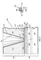
- FIG. 1An exemplary microwave circuit 20 is shown in FIG. 1, and FIGS. 2-4 illustrate a MMIC 100 in accordance with the present invention which realizes the exemplary circuit 20.
- the MMIC 100positions a distributed transmission-line network 110 over a microwave-device structure 130. Signal lines of the transmission-line network 110 are adapted to communicate with the microwave-device structure 130 through a ground plane of the network 110.
- the transmission-line network 110also includes a microwave dielectric which can be deposited in a thickness that is compatible with wide, low-loss signal lines.
- Each of the lines 36 and 38are configured to have a characteristic impedance of 70.7 ⁇ and have a length of 1/4 of the operating wavelength, i.e., they are quarter-wave transformers.
- the lines 36 and 38will each transform an impedance of 50 ⁇ at the circuit nodes 44 and 45 to 100 ⁇ at their opposite ends where they are coupled in parallel to the input transmission line 40.
- the set 112 of signal linesinclude all the transmission lines of the schematic 20.
- the input line 40positioned on the left side of the MMIC 100 are the input line 40, the power divider lines 36 and 38 and the impedance matching lines 54.
- the divider lines 36 and 38are thinner than the input line 40 and the impedance matching lines 54 which reflects the difference in their impedance, i.e., 70.7 ⁇ versus 50 ⁇ .
- the capacitors 56 and 52are realized at each end of the lines 54.
- the lines 79Positioned between the input and output transmission lines, are the lines 79 which couple the low, decoupling impedance of capacitors 78 at one end of the line to the transistor collectors which are reached through vias 119 at the other line end.
- the input and output ports 24 and 26are defined by pads 80 and 82.
- Other pads 106 at the top and bottom of the MMIC 100are spaced from the ground plane 112. They are available for connecting to other electrical forms, e.g., V + .
- the lumped and active elements of the schematic 20are carried on a silicon substrate 120 in the microwave-device structure 130. These elements include the transistors 22 and 23 and the resistors 74, 75 and 76. For clarity of illustration, only the transistor 23 is shown in FIG. 3.
- the transistor 23has an emitter ohmic contact 122, base ohmic contacts 124 and collector ohmic contacts 126.
- the microwave-device structure 130also includes an interconnect system 132 which has patterned layers 133 and 134 of conductive members, e.g., the members 138 and 139, which are separated by dielectric layers 135, 136 and 137 (the layers 133 and 134 are indicated by broken lines).
- the dielectricsare preferably chosen from materials, e.g., silicon dioxide and polyimide, which are well known to have low-loss microwave characteristics.
- the interconnect structure 132is also carried on the silicon substrate 120.
- the substrate 120is much thicker than the other structure of the MMIC 100 and is accordingly illustrated with a horizontal section removed.
- the MMIC 100would typically be mounted in a microwave package which is not shown for clarity of illustration. Connections, e.g., wirebonds, would typically be made between the pads 80, 82 and 106 to pins or transmission lines in the package perimeter. The MMIC 100 could then be integrated into a larger microwave circuit. Alternatively, the MMIC 100 could be mounted onto a larger substrate with other MMICs and be connected together to form a multi-chip module (MCM).
- MCMmulti-chip module
- the structure of the via 119can be formed by creating an opening in the dielectric 116 and continuing the plating of the transmission line 79 down into this opening.
- the pad 152may facilitate coupling the signal line portion 154 to the collector contact 126, it may be eliminated in other embodiments of the invention with the portion 154 brought directly into communication with the conductive member 138 by the interconnect via 156.
- FIG. 4is a view similar to FIG. 3 with like elements indicated by like reference numbers.
- This figureillustrates the structure of a transmission line ground as formed along the plane 4 - 4 of the ground pad 82 in FIG. 2.
- the spacing between a portion 174 of the signal line and the ground plane 114is eliminated, i.e., the signal line is plated down through an opening in the dielectric 116 to contact the ground plane.
- Many microwave circuitsrequire that transmission signal lines be terminated by a microwave short. These shorts can be formed as shown by the ground pad 82.
- Transmission signal linescan also form inductors as illustrated by the spiral inductor 180 of FIG. 5 which is positioned at the end of a signal line 182.
- the inductor 180is formed of a spiral shaped signal line 184 with ends 186 and 188.
- the ends of the inductorcan also have capacitor structures to the ground plane as in FIG. 3 or a microwave short as in FIG. 4.
- the signal lines, e.g., line 36, of the distributed transmission-line network 110 of FIGS. 2-4are preferably realized with a low-loss conductive metal that is compatible with MMIC fabrication, e.g., electroplated gold.
- low-loss conductive metals or alloys, e.g., aluminum-coppermay be advantageously used for the ground plane 114.
- the dielectric layer 118is the principle transmission-line dielectric. As such, it has a low dielectric constant and a low loss tangent. For ease of fabrication, it also should have good adhesion to substrates and metals.
- the dielectric 118can be deposited in relatively thick layers, e.g., at least 10 microns and, preferably, on the order of 13 microns, so that wide, low-loss signal lines can be realized. Finally, for consistent impedance it is desirable that the thickness of the dielectric be constant and that its upper surface is flat.
- the structures of the inventionare preferably realized with a dielectric that has the forgoing characteristics.
- An exemplary dielectric with these characteristicsis benzocyclobutene (BCB) which a has a dielectric constant of 2.65 and a loss tangent of 0.002 at 10GHz.
- BCBbenzocyclobutene
- This polymercan be deposited over a substrate by spin-coating. After the polymer is placed on a surface, the surface is rapidly spun which causes the BCB to assume a planar configuration. Openings in BCB can be fabricated by plasma etching or by reactive ion etching. Other embodiments of the invention can be formed with various dielectrics which have these desirable characteristics.
- the dielectric 117preferably has a high dielectric.
- Preferred dielectrics for this structureare silicon dioxide and silicon nitride.
- the transmission-line dielectric 116includes the additional layer adjoining the ground plane 114.
- An exemplary transmission linewas formed in accordance with the teachings of the invention. It had an electroplated gold signal line with a width of 3 micrometers and a length of 2450 micrometers. It was spaced from a ground plane by a 13 micron thick dielectric of BCB. In the graph 190 of FIG. 6, the measured loss in decibels/centimeter of this transmission line is plotted as the curve 192. The loss was also predicted by a calculation in which the dielectric constant was assumed to be 3.3 and the loss tangent assumed to be 0.025 (these measured parameters are different than the values above which were manufacturer's ratings). The calculated loss is shown as the broken line 193. The measured loss agrees best with the calculated loss in the region below 5GHz.
- An exemplary spiral inductor similar to the inductor 180 of FIG. 5was also fabricated. It had two turns of 10 micrometre wide signal lines over a BCB substrate. The measured inductance and quality factor Q are plotted in the graph 194 of FIG. 7 as the curves 196 and 197 respectively.
- the teachings of the inventionalso facilitate measurement of microwave device parameters prior to finalizing the MMIC fabrication.
- the parameters of the transistor 23could be measured with probes before deposition of the transmission-line network 110 over the microwave-device structure 130.
Landscapes
- Semiconductor Integrated Circuits (AREA)
- Microwave Amplifiers (AREA)
- Waveguides (AREA)
Description
- The present invention relates generally to monolithic microwaveintegrated circuits.
- The dual developments of compound semiconductors andheterostructure transistors have facilitated the improved frequencyperformance of microwave and millimeter-wave circuits. For example,superior high-frequency performance has been achieved by forming eachtransistor region of heterojunction bipolar transistors (HBTs) withsemiconductors of selected bandgaps. In an exemplary HBT, the emittersemiconductor is chosen to have a greater bandgap than the basesemiconductor. This allows the emitter to be heavily doped for increasedemitter efficiency and the base to be heavily doped and narrowed withoutincreasing base resistance. In addition, the collector semiconductor can bechosen to increase the transistor's breakdown voltage.
- Previously, realization of the advantages of heterostructure transistorswas primarily limited to the gallium aluminum arsenide/gallium arsenide(GaAlAs/GaAs) and indium gallium arsenide/indium phosphide (InGaAs/InP)semiconductor systems. The advantages of the GaAlAs/GaAs systeminclude an excellent lattice match, well-developed growth technologies(e.g., molecular beam epitaxy and metal-organic chemical vapordeposition), availability of large bandgap differences, high electronmobility, and a semi-insulating GaAs substrate. GaAlAs/GaAs HBTs have achieved unit current gain cutoff frequencies (fT) of 100GHz.
- The advantages of the InGaAs/InP system include a good latticematch, the same well-developed growth technologies of the GaAlAs/GaAssystem, an electron mobility even higher than GaAs, availability of evenlarger bandgaps, and a semi-insulating substrate of InP which has a goodthermal conductivity. HBTs in the InGaAs/InP system have achievedfTvalues of 165GHz.
- Conduction of microwave signals in these semiconductor systems istypically accomplished with microwave transmission structures such asmicrostrip. The dielectric of these structures preferably has a lowdielectric constant and a low loss tangent to reduce parasitic capacitancesand dielectric losses. Typically, the substrate of these semiconductorsystems has formed the dielectric of the microwave transmission lines.Substrates in the GaAlAs/GaAs and InGaAs/InP systems can be fabricatedwith high resistivities (e.g., 108Ω-cm) through the addition ofcarrier-trapping impurities such as chrome or iron. Accordingly, thesesubstrates can be used to form low-loss transmission lines.
- Recently, another semiconductor system has shown promise in themicrowave and millimeter-wave regions. This is the SiGe/Si system.GexSi1-x is an alloy with a lattice constant that is mismatched from Si.The SiGe/Si system has been shown to have excellent high-frequencyperformance. For example, Si/SiGe HBTs have achievedfT values of70GHz. In addition, silicon has far and away the most maturesemiconductor technology and enjoys a significant cost advantage overother semiconductor systems.
- However, in contrast with the GaAlAs/GaAs and InGaAs/InPsystems, the resistivity of silicon is limited (e.g., to -104Ω-cm) because theresistivity of silicon can only be increased by purification. Consequently,microwave transmission lines fabricated over silicon substrates produceundesirable losses. Primarily for this reason, MMICs constructed in thelow-cost SiGe/Si system have not exhibited competitive performance.
- Sakai, Hiroyuki, et al. have proposed (Sakai, H. et al., "A novelmillimeter-wave IC on Si Substrate",1994 IEEE MTT-S Digest, pp.1763-1766) a microstrip transmission line whose ground plane isfabricated on the surface of a highly-doped, silicon substrate. In thisstructure, millimeter-wave heterojunction transistor chips are inverted and bonded to signal lines of the transmission line. Althoughthis technique realizes microwave circuits with a low-costsilicon substrate, it fails to take advantage of the highyields and inherent cost savings of monolithic circuit fabrication.
EP 0 703 614 A2 which is state of the art relevant to thequestion of novelty only pursuant to Art. 54(3) and (4) EPC,discloses a flip-chip integrated circuit having passive as wellas active components on a surface of a substrate. A heat conductivelayer is formed over the active component for conductingheat away from the active component to a heat dissipatinglayer. A dielectric layer is formed over the passive component(preferably a transmission line) such that the surface of thedielectric layer is substantially planar with the conductivelayer.- Further microwave integrated circuits are disclosed in
EP 0 592 002 A2 and in US 5,202,752. - The present invention as claimed in claims 1 and 9 is directed to a monolithic microwaveintegrated circuit structure which combines low-loss microwavetransmission paths with semiconductor structures that are preferablysilicon-based for low-cost production. This goal is achieved with therecognition that a distributed, transmission-line network with a groundplane can be positioned over a semiconductor structure and signal lines ofthe transmission network adapted to communicate with the semiconductorsystem through the network's ground plane.
- In an embodiment, a microwave-device structure positionsmicrowave devices, e.g., silicon-based HBTs, on a silicon substrate andelectrically connects them through an interconnect system of alternatinglayers of conductive members and insulating dielectrics. The ground planeof a distributed, transmission-line network is carried over the interconnectsystem. Signal lines of the transmission network are spaced from theground plane by a microwave dielectric. An aperture is formed in theground plane and a signal line adapted to communicate with selectedmicrowave devices through the aperture. Alternatively, a pad can be left inthe aperture and the spacing between the pad and a signal line portionreduced to form a microwave capacitor.
- The loss through microstrip transmission lines is reduced when thesignal line width is increased and, to achieve a selected impedance, widerlines can be used if the spacing between the signal line and the groundplane is increased. Accordingly, the microwave dielectric isselected from materials, e.g., benzocyclobutene, that can be formed in athick planar layer, e.g., 13 microns.
- The novel features of the invention are set forth with particularity inthe appended claims. The invention will be best understood from thefollowing description when read in conjunction with the accompanyingdrawings.
- FIG. 1 is a schematic of an exemplary microwave amplifier circuit;
- FIG. 2 is a plan view of a monolithic microwave integrated circuit(MMIC) in accordance with the present invention, which realizes theschematic of FIG. 1;
- FIG. 3 is an enlarged view of MMIC structure along the plane 3 - 3 ofFIG. 2;
- FIG. 4 is an enlarged view of MMIC structure along the plane 4 - 4 ofFIG. 2;
- FIG. 5 is a plan view of a spiral inductor in accordance with thepresent invention;
- FIG. 6 is a graph of predicted and measured loss of a transmissionline in the MMIC of FIG. 2; and
- FIG. 7 is a graph of measured inductance and quality factor (Q) of thespiral inductor of FIG. 5.
- An
exemplary microwave circuit 20 is shown in FIG. 1, and FIGS. 2-4illustrate aMMIC 100 in accordance with the present invention whichrealizes theexemplary circuit 20. As particularly shown in FIG. 3, theMMIC 100 positions a distributed transmission-line network 110 over amicrowave-device structure 130. Signal lines of the transmission-linenetwork 110 are adapted to communicate with the microwave-devicestructure 130 through a ground plane of thenetwork 110. Thetransmission-line network 110 also includes a microwave dielectric whichcan be deposited in a thickness that is compatible with wide, low-losssignal lines. These structures facilitate the realization of the MMIC 100 ina silicon-based semiconductor system whose performance is comparablewith other high-speed semiconductor systems, e.g., GaAlAs/GaAs andInGaAs/InP, and whose fabrication costs are significantly less than thesesystems. Prior to a detailed description of theMMIC 100, attention is firstdirected to a preliminary description of the exemplary microwave circuitschematic 20, - The schematic 20 shows a microwave amplifier in which two
microwave transistors input port 24 and anoutput port 26. The bases ofthetransistors input port 24 by impedancematchingnetworks 28 and apower divider 30. The collectors of thetransistors output port 26 byimpedancematching networks 32 and a power combiner 34. The transistors' emittersare coupled to ground. - The
power divider 30 andpower combiner 34 are a type of circuitwhich is commonly called a Wilkinson power divider in the microwave art.Theinput divider 30 includes twotransmission lines input transmission line 40 and which arecoupled at another end by aresistive load 42. The ends of theload 42 areatcircuit nodes input port 24 and deliver it to thenodes circuit nodes input port 24. The impedance at the inputport is conventionally 50Ω and that is assumed to be the case in thecircuit 20 for clarity of description. - Each of the
lines lines circuit nodes input transmission line 40. - Because these impedances are in parallel, the
input line 40 ispresented with a 50Ω impedance. The input transmission line isconfigured to have a characteristic impedance of 50Ω so that it transformsthe impedance of the twolines input port 24. If theload 42 is selected to have an impedance of 100Ω, signals at the twocircuitnodes - The
impedance matching networks 28 are configured to transformthe input impedance of thetransistors circuitnodes networks 28 are assumed to include aseriescapacitor 52 andtransmission line 54 and ashunt capacitor 56. - The
impedance matching networks 32 and theoutput powercombiner 34 are configured in a manner similar to that described for thematching networks 28 andpower divider 30. Thepower combiner 34 hasparallel transmission lines circuit nodes 63 and64 to anoutput transmission line 66. The combiner also has anisolationresistor 67. Theimpedance matching networks 32 each include ashuntcapacitor 68 and aseries transmission line 70 and aseries capacitor 72. - Each of the
transistors resistors capacitor 78 and atransmission line 79 converts the lowimpedance of thedecoupling capacitor 78 to a suitable collector impedancefor the transistors. Each of theinput port 24 andoutput port 26 have asignal pad 80 and aground pad 82. - The
microwave circuit 20couples microwave transistors input port 24 and theoutput port 26. In operation, amicrowave signal received at theinput port 24 is divided into two portionswhich are separately amplified by thetransistors output port 26. Thetransistors impedance matching networks input circuit nodes output circuit nodes 63 and 64 into impedances at the base andcollector of thetransistors - Attention is now redirected to the
MMIC 100 as illustrated in FIGS.2-4. In these figures, theMMIC 100 is configured as a silicon-based,monolithic circuit which has a distributed transmission-line network 110(operation of distributed networks is described in terms of magnetic andelectric fields and the distributed network constants). Thenetwork 110 ispositioned over a lumped and active element circuit in the form of themicrowave-device structure 130. Thetransmission line structure 110includes a set oftransmission signal lines 112 which are spaced from aground plane 114 by amicrowave dielectric 116. The dielectric 116preferably has a thinfirst layer 117 adjacent theground plane 114 and athicker,second layer 118 adjacent the signal lines 112. Thetransmissionline network 110 is configured in conventional microstrip form, i.e., signal lines spaced above a ground plane by a dielectric. - In FIG. 2, the
set 112 of signal lines include all the transmission linesof the schematic 20. For example, positioned on the left side of theMMIC 100 are theinput line 40, the power divider lines 36 and 38 and theimpedance matching lines 54. The divider lines 36 and 38 are thinner thantheinput line 40 and theimpedance matching lines 54 which reflects thedifference in their impedance, i.e., 70.7Ω versus 50Ω. Thecapacitors lines 54. - Positioned on the right side of the
MMIC 100 are theoutput line 66,thepower combiner lines combiner lines output line 66 and the impedance matching lines 70. Thecapacitors lines 70. - Positioned between the input and output transmission lines, are the
lines 79 which couple the low, decoupling impedance ofcapacitors 78 atone end of the line to the transistor collectors which are reached throughvias 119 at the other line end. - The input and
output ports pads Other pads 106 at the top and bottom of theMMIC 100 are spaced fromtheground plane 112. They are available for connecting to other electricalforms, e.g., V+. - The lumped and active elements of the schematic 20 are carried on a
silicon substrate 120 in the microwave-device structure 130. Theseelements include thetransistors resistors transistor 23 is shown in FIG. 3. Thetransistor 23 has an emitterohmic contact 122, baseohmic contacts 124and collectorohmic contacts 126. - The microwave-
device structure 130 also includes aninterconnectsystem 132 which has patternedlayers members dielectriclayers layers interconnect structure 132 is also carried on thesilicon substrate 120. Thesubstrate 120 is much thicker than the otherstructure of theMMIC 100 and is accordingly illustrated with a horizontal section removed. - The
MMIC 100 would typically be mounted in a microwave packagewhich is not shown for clarity of illustration. Connections, e.g., wirebonds,would typically be made between thepads MMIC 100 could then beintegrated into a larger microwave circuit. Alternatively, theMMIC 100could be mounted onto a larger substrate with other MMICs and beconnected together to form a multi-chip module (MCM). - FIG. 3 illustrates the structure of the via 119 along the plane 3 - 3 ofFIG. 2. The figure shows an
aperture 150 in theground plane 114. Apad 152 of theground plane 114 is left within theaperture 150. The spacingbetween aportion 154 of thesignal line 79 and theground plane 114 iseliminated in the vicinity of theaperture 150. In particular, thesignal lineportion 154 is directed downward through the dielectric 118 to contact thepad 152. Thepad 152 is further connected through theconductive member 138 to one of the collectorohmic contacts 126 of thetransistor 23. Thisconnection is made through conventional viastructures 156 and 158(indicated by solid lines) between the layers of theinterconnect system 132. - The structure of the via 119 can be formed by creating an opening inthe dielectric 116 and continuing the plating of the
transmission line 79down into this opening. Although thepad 152 may facilitate coupling thesignal line portion 154 to thecollector contact 126, it may be eliminated inother embodiments of the invention with theportion 154 brought directlyinto communication with theconductive member 138 by the interconnectvia 156. - The
capacitor 72 is formed in a manner similar to that of thevia 119.Anaperture 160 is defined by theground plane 114 and apad 162 is left inthe aperture. Thecapacitor 72 is formed by reducing the spacing betweenaportion 164 of thesignal line 70 and thepad 162. Thespace 168 betweentheportion 164 and thepad 162 is adjusted so that thedielectric 117 forms the dielectric between the capacitor plates formed bytheportion 164 and thepad 162. Thepad 162 is connected to the othercollectorohmic contact 126 through theinterconnect member 139 andconventional vias interconnect system 132. In FIG. 3,the emitterohmic contact 122 is directly connected to theground plane 114. - FIG. 4 is a view similar to FIG. 3 with like elements indicated by likereference numbers. This figure illustrates the structure of a transmissionline ground as formed along the plane 4 - 4 of the
ground pad 82 in FIG. 2.The spacing between aportion 174 of the signal line and theground plane 114 is eliminated, i.e., the signal line is plated down through an opening inthe dielectric 116 to contact the ground plane. Many microwave circuits,require that transmission signal lines be terminated by a microwave short.These shorts can be formed as shown by theground pad 82. - Transmission signal lines can also form inductors as illustrated bythe
spiral inductor 180 of FIG. 5 which is positioned at the end of asignalline 182. Theinductor 180 is formed of a spiral shapedsignal line 184 withends - The signal lines, e.g.,
line 36, of the distributed transmission-linenetwork 110 of FIGS. 2-4 are preferably realized with a low-lossconductive metal that is compatible with MMIC fabrication, e.g.,electroplated gold. Similarly, low-loss conductive metals or alloys, e.g.,aluminum-copper, may be advantageously used for theground plane 114. - The
dielectric layer 118 is the principle transmission-line dielectric.As such, it has a low dielectric constant and a low loss tangent.For ease of fabrication, it also should have good adhesion to substrates andmetals. - Increasing the signal line widths, e.g., the
width 189 in FIG. 2, lowersthe microwave path losses of the transmission-line network 110. For agiven transmission-line impedance, an increased spacing between thesignal line and the ground plane requires an increased width of the line.Therefore, another preferred characteristic of the dielectric 118 is that itcan be deposited in relatively thick layers, e.g., at least 10 microns and,preferably, on the order of 13 microns, so that wide, low-loss signal linescan be realized. Finally, for consistent impedance it is desirable that thethickness of the dielectric be constant and that its upper surface is flat. - The structures of the invention are preferably realized with adielectric that has the forgoing characteristics. An exemplary dielectricwith these characteristics is benzocyclobutene (BCB) which a has a dielectric constant of 2.65 and a loss tangent of 0.002 at 10GHz. This polymercan be deposited over a substrate by spin-coating. After the polymer is placedon a surface, the surface is rapidly spun which causes the BCB to assume aplanar configuration. Openings in BCB can be fabricated by plasma etching orby reactive ion etching. Other embodiments of the invention can be formedwith various dielectrics which have these desirable characteristics.
- In order to reduce the lateral extent of the
capacitor plates line dielectric 116 includes the additional layeradjoining theground plane 114. - An exemplary transmission line was formed in accordance with theteachings of the invention. It had an electroplated gold signal line with a widthof 3 micrometers and a length of 2450 micrometers. It was spaced from a ground planeby a 13 micron thick dielectric of BCB. In the
graph 190 of FIG. 6, themeasured loss in decibels/centimeter of this transmission line is plotted as thecurve 192. The loss was also predicted by a calculation in which the dielectricconstant was assumed to be 3.3 and the loss tangent assumed to be 0.025(these measured parameters are different than the values above which weremanufacturer's ratings). The calculated loss is shown as thebroken line 193.The measured loss agrees best with the calculated loss in the region below5GHz. - An exemplary spiral inductor similar to the
inductor 180 of FIG. 5 wasalso fabricated. It had two turns of 10 micrometre wide signal lines over a BCBsubstrate. The measured inductance and quality factor Q are plotted in thegraph 194 of FIG. 7 as thecurves - In accordance with customary practice, the term monolithic microwaveintegrated circuit (MMIC) has been used in this description to refer tomonolithic circuits which are intended to operate at frequencies above 1 GHz.The term millimeter wave generally is used to refer to frequencies in the rangeof 40 GHz to 300 GHz (IEEE Standard 521-1976). Thus, millimeter wavefrequencies are a subset of microwave frequencies and are inherently includedin the use of the term MMIC.
- Although the
signal line portions - The teachings of the invention facilitate the combination ofsilicon-based devices and silicon substrates with low-loss transmission linenetworks. Thus, MMICs can include high frequency transistor structures,e.g., HBTs, which are fabricated in semiconductor systems e.g., GeSi/Si,that are less expensive than previously preferred systems such asGaAlAs/GaAs and InGaAs/InP.
- The teachings of the invention also facilitate measurement ofmicrowave device parameters prior to finalizing the MMIC fabrication. Forexample, in FIG. 3 the parameters of the
transistor 23 could be measuredwith probes before deposition of the transmission-line network 110 overthe microwave-device structure 130.
Claims (9)
- A monolithic microwave integrated circuit, comprising:characterized in that said transmission-line dielectric(116) includes a first layer (118) with a low dielectric constant,and a second layer (117) with a high dielectric constant, said second layer (117) being positioned between saidground plane (114) and said first layer (118).a distributed, transmission-line network (110)having a ground plane (114), being configuredto conduct microwave signals and includinga plurality of microwave signal lines(112) spaced above said ground plane (114);anda transmission-line dielectric (116) betweensaid signal lines (112) and said groundplane (114);a microwave-device structure (130) which has:a) a semiconductor substrate (120),b) a plurality of microwave devices that arecarried on said substrate (120), andc) an interconnect system (132) which is carriedon said substrate (120) and configuredto electrically connect said microwave devices;wherein said transmission-line network(110) is carried over said interconnectsystem (132) and is adapted to communicatethrough said ground plane (114) with predetermineddevices of said microwave-devicestructure (130);
- The circuit of claim 1,characterized in that saidground plane (114) defines an aperture (150), and that one ofsaid signal lines (112) is adapted to communicate with said microwave-devicestructure (130) through said aperture (150).
- The circuit of claim 1 or 2,characterized in thatsaid signal lines (112) are generally spaced greater than 10micrometers from said ground plane (114).
- The circuit of any of claims 1 - 3,characterized inthat the spacing (168) between a portion (164) of said signallines (112) and said ground plane (114) is locally reduced toform a microwave capacitor (72).
- The circuit of claim 4,characterized in that saidfirst layer (118) is of benzocyclobutene; and said second layer(117) is of silicon nitride which is positioned between saidsignal line portion (164) and said ground plane (114).
- The circuit of any of claims 1 - 5,characterized inthat the spacing between one of said signal lines (112) andsaid ground plane (114) is locally eliminated to form a microwaveshort (82).
- The circuit of any of claims 1 - 6,characterized inthat said transmission-line dielectric (116) comprises benzocyclobutene.
- The circuit of any of claims 1 - 7,characterized inthat said interconnect system (132) includes:at least one layer of conductive members (133,134); andan interconnect dielectric (135, 136, 137) arrangedto insulate said conductive members(133, 134).
- A method of communicating between a distributedtransmission line (112) and a microwave device carried on asubstrate (120) in a monolithic microwave integrated circuit,comprising the steps of:positioning a ground plane (114) of said transmissionline (112) between a signal line (70)of said transmission line (112) and said microwavedevice;positioning a first dielectric layer (117) witha high dielectric constant on said ground plane(114) and a second dielectric layer (118) witha low dielectric constant on said first dielectriclayer (117);forming an aperture (150) in said ground plane(114); andadapting said signal line (70) to communicate through saidaperture (150) with said microwave device, wherein, preferably,said adapting step includes the step of positioning a portionof said signal line (70) adjacent said aperture (150).
Applications Claiming Priority (2)
| Application Number | Priority Date | Filing Date | Title |
|---|---|---|---|
| US430067 | 1995-04-27 | ||
| US08/430,067US5528209A (en) | 1995-04-27 | 1995-04-27 | Monolithic microwave integrated circuit and method |
Publications (3)
| Publication Number | Publication Date |
|---|---|
| EP0741414A2 EP0741414A2 (en) | 1996-11-06 |
| EP0741414A3 EP0741414A3 (en) | 1998-10-21 |
| EP0741414B1true EP0741414B1 (en) | 2002-06-05 |
Family
ID=23705930
Family Applications (1)
| Application Number | Title | Priority Date | Filing Date |
|---|---|---|---|
| EP96106512AExpired - LifetimeEP0741414B1 (en) | 1995-04-27 | 1996-04-25 | Monolithic microwave integrated circuit and method |
Country Status (4)
| Country | Link |
|---|---|
| US (1) | US5528209A (en) |
| EP (1) | EP0741414B1 (en) |
| JP (1) | JPH0917959A (en) |
| DE (1) | DE69621517T2 (en) |
Families Citing this family (64)
| Publication number | Priority date | Publication date | Assignee | Title |
|---|---|---|---|---|
| US6372534B1 (en)* | 1995-06-06 | 2002-04-16 | Lg. Philips Lcd Co., Ltd | Method of making a TFT array with photo-imageable insulating layer over address lines |
| US5994721A (en)* | 1995-06-06 | 1999-11-30 | Ois Optical Imaging Systems, Inc. | High aperture LCD with insulating color filters overlapping bus lines on active substrate |
| US5883422A (en)* | 1996-06-28 | 1999-03-16 | The Whitaker Corporation | Reduced parasitic capacitance semiconductor devices |
| US6310394B1 (en)* | 1996-06-28 | 2001-10-30 | Tyco Electronics | Reduced parasitic capacitance semiconductor devices |
| JPH10163772A (en)* | 1996-10-04 | 1998-06-19 | Sanyo Electric Co Ltd | Power amplifier and chip carrier |
| JP4330919B2 (en)* | 1997-03-14 | 2009-09-16 | 株式会社東芝 | Microwave integrated circuit element |
| US5886597A (en)* | 1997-03-28 | 1999-03-23 | Virginia Tech Intellectual Properties, Inc. | Circuit structure including RF/wideband resonant vias |
| US5945734A (en)* | 1997-09-19 | 1999-08-31 | Samsung Electronics Co., Ltd. | Wire-bond free input/output interface for GaAs ICs with means of determining known good die |
| US6359672B2 (en) | 1997-10-20 | 2002-03-19 | Guardian Industries Corp. | Method of making an LCD or X-ray imaging device with first and second insulating layers |
| US6011274A (en)* | 1997-10-20 | 2000-01-04 | Ois Optical Imaging Systems, Inc. | X-ray imager or LCD with bus lines overlapped by pixel electrodes and dual insulating layers therebetween |
| FR2793008B1 (en)* | 1999-04-30 | 2001-07-27 | Valeurs Bois Ind | PROCESS FOR THE EXTRACTION OF NATURAL JUICE FROM WOODY PLANT MATERIAL, DEVICE FOR CARRYING OUT THE PROCESS AND USE OF THE PROCESS FOR THE PRODUCTION OF DRY WOODY PLANT |
| EP0940848A3 (en)* | 1998-03-05 | 2000-03-22 | Interuniversitair Micro-Elektronica Centrum Vzw | A low-loss conductive pattern and a method for fabrication thereof |
| US6259148B1 (en)* | 1998-08-13 | 2001-07-10 | International Business Machines Corporation | Modular high frequency integrated circuit structure |
| US6222246B1 (en)* | 1999-01-08 | 2001-04-24 | Intel Corporation | Flip-chip having an on-chip decoupling capacitor |
| US6693033B2 (en)* | 2000-02-10 | 2004-02-17 | Motorola, Inc. | Method of removing an amorphous oxide from a monocrystalline surface |
| US6392257B1 (en) | 2000-02-10 | 2002-05-21 | Motorola Inc. | Semiconductor structure, semiconductor device, communicating device, integrated circuit, and process for fabricating the same |
| JP2004503920A (en) | 2000-05-31 | 2004-02-05 | モトローラ・インコーポレイテッド | Semiconductor device and method of manufacturing the semiconductor device |
| US20020008234A1 (en)* | 2000-06-28 | 2002-01-24 | Motorola, Inc. | Mixed-signal semiconductor structure, device including the structure, and methods of forming the device and the structure |
| WO2002009187A2 (en) | 2000-07-24 | 2002-01-31 | Motorola, Inc. | Heterojunction tunneling diodes and process for fabricating same |
| US20020096683A1 (en)* | 2001-01-19 | 2002-07-25 | Motorola, Inc. | Structure and method for fabricating GaN devices utilizing the formation of a compliant substrate |
| KR20020070739A (en)* | 2001-03-03 | 2002-09-11 | 삼성전자 주식회사 | MMIC and method for manufacturing the same |
| WO2002082551A1 (en) | 2001-04-02 | 2002-10-17 | Motorola, Inc. | A semiconductor structure exhibiting reduced leakage current |
| TW546819B (en)* | 2001-05-30 | 2003-08-11 | Sharp Kk | Semiconductor device, manufacturing method thereof, and monolithic microwave integrated circuit |
| US6709989B2 (en) | 2001-06-21 | 2004-03-23 | Motorola, Inc. | Method for fabricating a semiconductor structure including a metal oxide interface with silicon |
| US6992321B2 (en) | 2001-07-13 | 2006-01-31 | Motorola, Inc. | Structure and method for fabricating semiconductor structures and devices utilizing piezoelectric materials |
| US7019332B2 (en)* | 2001-07-20 | 2006-03-28 | Freescale Semiconductor, Inc. | Fabrication of a wavelength locker within a semiconductor structure |
| US6693298B2 (en) | 2001-07-20 | 2004-02-17 | Motorola, Inc. | Structure and method for fabricating epitaxial semiconductor on insulator (SOI) structures and devices utilizing the formation of a compliant substrate for materials used to form same |
| US6855992B2 (en) | 2001-07-24 | 2005-02-15 | Motorola Inc. | Structure and method for fabricating configurable transistor devices utilizing the formation of a compliant substrate for materials used to form the same |
| US20030026310A1 (en)* | 2001-08-06 | 2003-02-06 | Motorola, Inc. | Structure and method for fabrication for a lighting device |
| US6639249B2 (en)* | 2001-08-06 | 2003-10-28 | Motorola, Inc. | Structure and method for fabrication for a solid-state lighting device |
| US20030034491A1 (en) | 2001-08-14 | 2003-02-20 | Motorola, Inc. | Structure and method for fabricating semiconductor structures and devices for detecting an object |
| US6673667B2 (en)* | 2001-08-15 | 2004-01-06 | Motorola, Inc. | Method for manufacturing a substantially integral monolithic apparatus including a plurality of semiconductor materials |
| US20030071327A1 (en) | 2001-10-17 | 2003-04-17 | Motorola, Inc. | Method and apparatus utilizing monocrystalline insulator |
| JP3674780B2 (en)* | 2001-11-29 | 2005-07-20 | ユーディナデバイス株式会社 | High frequency semiconductor device |
| US6916717B2 (en) | 2002-05-03 | 2005-07-12 | Motorola, Inc. | Method for growing a monocrystalline oxide layer and for fabricating a semiconductor device on a monocrystalline substrate |
| US7169619B2 (en)* | 2002-11-19 | 2007-01-30 | Freescale Semiconductor, Inc. | Method for fabricating semiconductor structures on vicinal substrates using a low temperature, low pressure, alkaline earth metal-rich process |
| US6885065B2 (en) | 2002-11-20 | 2005-04-26 | Freescale Semiconductor, Inc. | Ferromagnetic semiconductor structure and method for forming the same |
| US6806202B2 (en) | 2002-12-03 | 2004-10-19 | Motorola, Inc. | Method of removing silicon oxide from a surface of a substrate |
| US6963090B2 (en)* | 2003-01-09 | 2005-11-08 | Freescale Semiconductor, Inc. | Enhancement mode metal-oxide-semiconductor field effect transistor |
| US6965128B2 (en) | 2003-02-03 | 2005-11-15 | Freescale Semiconductor, Inc. | Structure and method for fabricating semiconductor microresonator devices |
| NL1027745C1 (en)* | 2004-12-14 | 2006-06-16 | Bosma Beheersmij B V H O D N M | Low-loss, asymmetrical combinator for phase difference systems and adaptive RF amplifier comprising an asymmetrical combiner. |
| US8324660B2 (en) | 2005-05-17 | 2012-12-04 | Taiwan Semiconductor Manufacturing Company, Ltd. | Lattice-mismatched semiconductor structures with reduced dislocation defect densities and related methods for device fabrication |
| US9153645B2 (en) | 2005-05-17 | 2015-10-06 | Taiwan Semiconductor Manufacturing Company, Ltd. | Lattice-mismatched semiconductor structures with reduced dislocation defect densities and related methods for device fabrication |
| WO2007112066A2 (en) | 2006-03-24 | 2007-10-04 | Amberwave Systems Corporation | Lattice-mismatched semiconductor structures and related methods for device fabrication |
| US8173551B2 (en) | 2006-09-07 | 2012-05-08 | Taiwan Semiconductor Manufacturing Co., Ltd. | Defect reduction using aspect ratio trapping |
| WO2008039534A2 (en) | 2006-09-27 | 2008-04-03 | Amberwave Systems Corporation | Quantum tunneling devices and circuits with lattice- mismatched semiconductor structures |
| US8502263B2 (en) | 2006-10-19 | 2013-08-06 | Taiwan Semiconductor Manufacturing Company, Ltd. | Light-emitter-based devices with lattice-mismatched semiconductor structures |
| US8304805B2 (en) | 2009-01-09 | 2012-11-06 | Taiwan Semiconductor Manufacturing Company, Ltd. | Semiconductor diodes fabricated by aspect ratio trapping with coalesced films |
| US7825328B2 (en) | 2007-04-09 | 2010-11-02 | Taiwan Semiconductor Manufacturing Company, Ltd. | Nitride-based multi-junction solar cell modules and methods for making the same |
| WO2008124154A2 (en) | 2007-04-09 | 2008-10-16 | Amberwave Systems Corporation | Photovoltaics on silicon |
| US8237151B2 (en) | 2009-01-09 | 2012-08-07 | Taiwan Semiconductor Manufacturing Company, Ltd. | Diode-based devices and methods for making the same |
| US8329541B2 (en) | 2007-06-15 | 2012-12-11 | Taiwan Semiconductor Manufacturing Company, Ltd. | InP-based transistor fabrication |
| JP2010538495A (en) | 2007-09-07 | 2010-12-09 | アンバーウェーブ・システムズ・コーポレーション | Multi-junction solar cell |
| JP5337041B2 (en)* | 2007-10-09 | 2013-11-06 | パナソニック株式会社 | Circuit equipment |
| US8183667B2 (en) | 2008-06-03 | 2012-05-22 | Taiwan Semiconductor Manufacturing Co., Ltd. | Epitaxial growth of crystalline material |
| US8274097B2 (en) | 2008-07-01 | 2012-09-25 | Taiwan Semiconductor Manufacturing Company, Ltd. | Reduction of edge effects from aspect ratio trapping |
| US8981427B2 (en) | 2008-07-15 | 2015-03-17 | Taiwan Semiconductor Manufacturing Company, Ltd. | Polishing of small composite semiconductor materials |
| EP2335273A4 (en) | 2008-09-19 | 2012-01-25 | Taiwan Semiconductor Mfg | FORMATION OF DEVICES BY GROWTH OF EPITAXIAL LAYERS |
| US20100072515A1 (en) | 2008-09-19 | 2010-03-25 | Amberwave Systems Corporation | Fabrication and structures of crystalline material |
| US8253211B2 (en) | 2008-09-24 | 2012-08-28 | Taiwan Semiconductor Manufacturing Company, Ltd. | Semiconductor sensor structures with reduced dislocation defect densities |
| JP2010205941A (en) | 2009-03-03 | 2010-09-16 | Panasonic Corp | Semiconductor chip, and semiconductor device |
| US8629446B2 (en) | 2009-04-02 | 2014-01-14 | Taiwan Semiconductor Manufacturing Company, Ltd. | Devices formed from a non-polar plane of a crystalline material and method of making the same |
| US9912303B2 (en)* | 2010-02-03 | 2018-03-06 | Massachusetts Institute Of Technology | RF-input / RF-output outphasing amplifier |
| FI130081B (en) | 2019-03-18 | 2023-01-31 | Teknologian Tutkimuskeskus Vtt Oy | Wilkinson divider |
Family Cites Families (6)
| Publication number | Priority date | Publication date | Assignee | Title |
|---|---|---|---|---|
| US4967201A (en)* | 1987-10-22 | 1990-10-30 | Westinghouse Electric Corp. | Multi-layer single substrate microwave transmit/receive module |
| US5040047A (en)* | 1989-12-26 | 1991-08-13 | General Electric Company | Enhanced fluorescence polymers and interconnect structures using them |
| US5202752A (en)* | 1990-05-16 | 1993-04-13 | Nec Corporation | Monolithic integrated circuit device |
| JPH06125208A (en)* | 1992-10-09 | 1994-05-06 | Mitsubishi Electric Corp | Microwave integrated circuit and its production |
| JPH0758526A (en)* | 1993-08-10 | 1995-03-03 | Nippon Telegr & Teleph Corp <Ntt> | Integrated circuit |
| US5521406A (en)* | 1994-08-31 | 1996-05-28 | Texas Instruments Incorporated | Integrated circuit with improved thermal impedance |
- 1995
- 1995-04-27USUS08/430,067patent/US5528209A/ennot_activeExpired - Lifetime
- 1996
- 1996-04-25EPEP96106512Apatent/EP0741414B1/ennot_activeExpired - Lifetime
- 1996-04-25DEDE69621517Tpatent/DE69621517T2/ennot_activeExpired - Lifetime
- 1996-04-26JPJP8106894Apatent/JPH0917959A/enactivePending
Also Published As
| Publication number | Publication date |
|---|---|
| DE69621517D1 (en) | 2002-07-11 |
| JPH0917959A (en) | 1997-01-17 |
| EP0741414A3 (en) | 1998-10-21 |
| US5528209A (en) | 1996-06-18 |
| DE69621517T2 (en) | 2002-09-26 |
| EP0741414A2 (en) | 1996-11-06 |
Similar Documents
| Publication | Publication Date | Title |
|---|---|---|
| EP0741414B1 (en) | Monolithic microwave integrated circuit and method | |
| US6331931B1 (en) | Radio frequency power device improvement | |
| US10637400B2 (en) | RF amplifier with conductor-less region underlying filter circuit inductor, and methods of manufacture thereof | |
| US10630246B2 (en) | Methods of manufacturing encapsulated semiconductor device package with heatsink opening | |
| US5614442A (en) | Method of making flip-chip microwave integrated circuit | |
| US9721909B1 (en) | Hybrid microwave integrated circuit | |
| US8669638B2 (en) | High power semiconductor device for wireless applications and method of forming a high power semiconductor device | |
| US12308355B2 (en) | Semiconductor device and semiconductor module | |
| US4673958A (en) | Monolithic microwave diodes | |
| WO2021202199A1 (en) | Group iii nitride-based radio frequency amplifiers having back side source, gate and/or drain terminals | |
| EP0508128B1 (en) | Four port monolithic GaAs PIN diode switch | |
| US20230207558A1 (en) | Microwave integrated circuits including gallium-nitride devices on silicon | |
| WO2022260855A1 (en) | Packaged transistor amplifier with integrated passive device matching structure having distributed shunt inductances | |
| US4859633A (en) | Process for fabricating monolithic microwave diodes | |
| CA3186877A1 (en) | Impedance matching using kinetic inductors | |
| US6825809B2 (en) | High-frequency semiconductor device | |
| US6285269B1 (en) | High-frequency semiconductor device having microwave transmission line being formed by a gate electrode source electrode and a dielectric layer in between | |
| US5683919A (en) | Transistor and circuit incorporating same | |
| EP4369398A2 (en) | Power amplifier device having vertical die interconnect structure | |
| Tserng et al. | Embedded transmission-line (ETL) MMIC for low-cost high-density wireless communication applications | |
| JPH10289979A (en) | High frequency semiconductor devices | |
| Hill et al. | Low thermal impedance MMIC technology | |
| JP2674750B2 (en) | Semiconductor device | |
| Guthrie et al. | A 50 mm copper/polymer substrate HBT IC technology for> 100 GHz MMICs | |
| Li et al. | A new technology for Si microwave power transistor manufacturing |
Legal Events
| Date | Code | Title | Description |
|---|---|---|---|
| PUAI | Public reference made under article 153(3) epc to a published international application that has entered the european phase | Free format text:ORIGINAL CODE: 0009012 | |
| AK | Designated contracting states | Kind code of ref document:A2 Designated state(s):DE FR GB | |
| PUAL | Search report despatched | Free format text:ORIGINAL CODE: 0009013 | |
| AK | Designated contracting states | Kind code of ref document:A3 Designated state(s):DE FR GB | |
| RAP1 | Party data changed (applicant data changed or rights of an application transferred) | Owner name:HUGHES ELECTRONICS CORPORATION | |
| 17P | Request for examination filed | Effective date:19990326 | |
| 17Q | First examination report despatched | Effective date:20000608 | |
| GRAG | Despatch of communication of intention to grant | Free format text:ORIGINAL CODE: EPIDOS AGRA | |
| GRAG | Despatch of communication of intention to grant | Free format text:ORIGINAL CODE: EPIDOS AGRA | |
| GRAH | Despatch of communication of intention to grant a patent | Free format text:ORIGINAL CODE: EPIDOS IGRA | |
| GRAH | Despatch of communication of intention to grant a patent | Free format text:ORIGINAL CODE: EPIDOS IGRA | |
| GRAA | (expected) grant | Free format text:ORIGINAL CODE: 0009210 | |
| AK | Designated contracting states | Kind code of ref document:B1 Designated state(s):DE FR GB | |
| REG | Reference to a national code | Ref country code:GB Ref legal event code:FG4D | |
| REF | Corresponds to: | Ref document number:69621517 Country of ref document:DE Date of ref document:20020711 | |
| ET | Fr: translation filed | ||
| ET | Fr: translation filed | ||
| PLBE | No opposition filed within time limit | Free format text:ORIGINAL CODE: 0009261 | |
| STAA | Information on the status of an ep patent application or granted ep patent | Free format text:STATUS: NO OPPOSITION FILED WITHIN TIME LIMIT | |
| 26N | No opposition filed | Effective date:20030306 | |
| REG | Reference to a national code | Ref country code:FR Ref legal event code:PLFP Year of fee payment:20 | |
| PGFP | Annual fee paid to national office [announced via postgrant information from national office to epo] | Ref country code:GB Payment date:20150420 Year of fee payment:20 Ref country code:DE Payment date:20150421 Year of fee payment:20 | |
| PGFP | Annual fee paid to national office [announced via postgrant information from national office to epo] | Ref country code:FR Payment date:20150421 Year of fee payment:20 | |
| REG | Reference to a national code | Ref country code:DE Ref legal event code:R071 Ref document number:69621517 Country of ref document:DE | |
| REG | Reference to a national code | Ref country code:GB Ref legal event code:PE20 Expiry date:20160424 | |
| PG25 | Lapsed in a contracting state [announced via postgrant information from national office to epo] | Ref country code:GB Free format text:LAPSE BECAUSE OF EXPIRATION OF PROTECTION Effective date:20160424 |