EP0739097B1 - MOSFET circuit and CMOS logic circuit using the same - Google Patents
MOSFET circuit and CMOS logic circuit using the sameDownload PDFInfo
- Publication number
- EP0739097B1 EP0739097B1EP96106128AEP96106128AEP0739097B1EP 0739097 B1EP0739097 B1EP 0739097B1EP 96106128 AEP96106128 AEP 96106128AEP 96106128 AEP96106128 AEP 96106128AEP 0739097 B1EP0739097 B1EP 0739097B1
- Authority
- EP
- European Patent Office
- Prior art keywords
- mosfet
- circuit
- threshold voltage
- voltage
- mosfets
- Prior art date
- Legal status (The legal status is an assumption and is not a legal conclusion. Google has not performed a legal analysis and makes no representation as to the accuracy of the status listed.)
- Expired - Lifetime
Links
- 230000003071parasitic effectEffects0.000claimsdescription11
- 238000010586diagramMethods0.000description30
- 239000004065semiconductorSubstances0.000description12
- 239000000758substrateSubstances0.000description12
- 230000000694effectsEffects0.000description9
- 230000005540biological transmissionEffects0.000description6
- 230000007423decreaseEffects0.000description6
- 230000008901benefitEffects0.000description5
- 230000006870functionEffects0.000description5
- 230000009467reductionEffects0.000description5
- 230000005669field effectEffects0.000description4
- 230000000295complement effectEffects0.000description3
- 229910052710siliconInorganic materials0.000description3
- 239000010703siliconSubstances0.000description3
- XUIMIQQOPSSXEZ-UHFFFAOYSA-NSiliconChemical compound[Si]XUIMIQQOPSSXEZ-UHFFFAOYSA-N0.000description2
- 230000003247decreasing effectEffects0.000description2
- 239000002184metalSubstances0.000description2
- 229910052751metalInorganic materials0.000description2
- 238000000034methodMethods0.000description2
- 230000003068static effectEffects0.000description2
- 230000009471actionEffects0.000description1
- 230000008859changeEffects0.000description1
- 238000011161developmentMethods0.000description1
- 230000018109developmental processEffects0.000description1
- 239000012212insulatorSubstances0.000description1
- 230000010354integrationEffects0.000description1
- 238000004519manufacturing processMethods0.000description1
- 150000002739metalsChemical class0.000description1
- 230000008569processEffects0.000description1
Images


Classifications
- H—ELECTRICITY
- H03—ELECTRONIC CIRCUITRY
- H03K—PULSE TECHNIQUE
- H03K19/00—Logic circuits, i.e. having at least two inputs acting on one output; Inverting circuits
- H03K19/0008—Arrangements for reducing power consumption
- H03K19/0016—Arrangements for reducing power consumption by using a control or a clock signal, e.g. in order to apply power supply
- H—ELECTRICITY
- H03—ELECTRONIC CIRCUITRY
- H03K—PULSE TECHNIQUE
- H03K19/00—Logic circuits, i.e. having at least two inputs acting on one output; Inverting circuits
- H03K19/003—Modifications for increasing the reliability for protection
- H03K19/00346—Modifications for eliminating interference or parasitic voltages or currents
- H03K19/00361—Modifications for eliminating interference or parasitic voltages or currents in field effect transistor circuits
- H—ELECTRICITY
- H10—SEMICONDUCTOR DEVICES; ELECTRIC SOLID-STATE DEVICES NOT OTHERWISE PROVIDED FOR
- H10D—INORGANIC ELECTRIC SEMICONDUCTOR DEVICES
- H10D89/00—Aspects of integrated devices not covered by groups H10D84/00 - H10D88/00
- H10D89/211—Design considerations for internal polarisation
- H10D89/213—Design considerations for internal polarisation in field-effect devices
Definitions
- the present inventionrelates to a MOSFET that can achieve high speed operation and low power consumption in a wide supply voltage range from low to high voltages, and particularly to a MOSFET suitable for an SOI (Silicon On Insulator) integrated circuit, and CMOS logic circuits using this MOSFET.
- SOISilicon On Insulator
- a conventional low voltage CMOS logic circuitis disclosed in Japanese patent application laying-open No. 29834/1994.
- the CMOS logic circuitcan operate with 1V battery supply by combining a plurality of MOSFETs of a low threshold voltage (of about 0.2V) and a high threshold voltage (of about 0.6V) as shown in Fig. 1.
- the circuitis an ingenious combination of low threshold voltage MOSFETs and high threshold voltage MOSFETs, the former being capable of high speed operation at the cost of a large leakage current in the non-conductive state, whereas the latter having small leakage current in the non-conductive state at the cost of a low operating speed.
- the circuitincludes a quasi-high-potential (VDDv) power supply line 41 and a quasi-low-potential (VDDs) power supply line 51 in addition to a high-potential (VDD) power supply line 1 and a low-potential (VSS) power supply line 2 which is normally grounded as shown in Fig. 1.
- VDDvquasi-high-potential
- VDDsquasi-low-potential
- VSSlow-potential
- CMOS logic circuit 3is connected which comprises low threshold voltage p-channel MOSFETs M11 and n-channel MOSFETs M12.
- a p-channel MOSFET M13is connected between the quasi-high-potential power supply line 41 and the high-potential power supply line 1
- an n-channel MOSFET M14is connected between the quasi-low-potential power supply line 51 and the low-potential power supply line 2.
- the reference numeral 4designates a high-potential power supply controller including MOSFET M13 and the quasi-high-potential power supply line 41
- the reference numeral 5denotes a low-potential power supply controller including the MOSFET M14 and the quasi-low-potential power supply line 51.
- the CMOS logic circuit 3is arranged with the low threshold voltage MOSFETs M11 and M12, and this enables a high speed operation with a low supply voltage.
- the power supply passage to the low threshold voltage CMOS logic circuit 3is provided with the high threshold voltage p-channel MOSFET M13 and n-channel MOSFET M14, the leakage current to the CMOS logic circuit 3 is prevented from flowing in a sleep mode (with a sleep signal SL at "H" level), thereby reducing the power consumption.
- *SLdenotes the inverted signal of the sleep signal SL.
- Fig. 2shows another circuit proposed in U.S. patent application No. 08/495,785. This is an improved circuit of Fig. 1, in which the high-potential and low-potential power supply controllers 4 and 5 are provided with the MOSFETs M13 and M14 with their backgate (substrate) terminals connected to their gate terminals.
- the same integrated circuitmay be used not only with a low voltage power supply, but also with a wide supply voltage range from less than 1V up to 3V to 5V.
- n-channel MOSFET M14for controlling the power supply in Fig. 2.
- the following explanationcan be applied to the other high threshold voltage MOSFET M13 in a similar manner.
- the n-channel MOSFET M14has a p-semiconductor backgate region (a substrate or well in a bulk MOS structure).
- a parasitic diode D3is formed across the backgate region B and the source S.
- the MOSFET M14 as shown in Fig. 3Ahas an equivalent circuit as shown in Fig. 3B.
- the parasitic diode D3will conduct when the gate-source voltage Vgs of the MOSFET M14 exceeds the forward voltage Vf of the parasitic diode D3.
- the forward voltage Vfis defined as a voltage at which current begins to flow through the diode 3 when an increasing forward voltage is applied thereto, and is about 0.8V in this case.
- a passageis formed through the gate terminal, backgate terminal and parasitic diode D3, thereby sharply increasing the gate current.
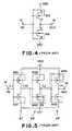
- Fig. 4shows a conventional example of a CMOS logic circuit capable of operating at a high speed with a supply voltage less than 1V close to the threshold voltage of the MOSFETs.
- the circuitis taught by T. Andoh, et al., "Design Methodology for Low-Voltage MOSFETs", IEDM Technical Digest, pp. 79-82, 1994.
- the circuit of Fig. 4is a CMOS inverter consisting of a p-channel MOSFET M3 and an n-channel MOSFET M4, with their gate terminals and backgate terminals connected in common.
- the reference numerals 14 and 15denote a signal input terminal and a signal output terminal, respectively.
- the backgate region (n-type semiconductor) and the source region (p-type semiconductor)are forwardly biased in the p-channel MOSFET M3, when a low level voltage (equal to ground voltage) is applied to the gate terminal via the signal input terminal 14 because the voltage of the backgate terminal connected to the gate terminal is also reduced.
- the backgate region (p-type semiconductor) and the source region (n-type semiconductor)are forwardly biased in the n-channel MOSFET M4, when a high level voltage (equal to the supply voltage VDD) is applied to the gate terminal via the signal input terminal 14 because the voltage of the backgate terminal connected to the gate terminal is also increased.
- the forward bias applied across the backgate region and the source regionwill reduce the depletion layer in the backgate region.
- the threshold voltage of a MOSFETis determined by a ratio of the charge density Q B to the gate capacitance Cox, and hence the threshold voltage decreases with a reduction in the depletion layer width and Q B . In this case, the absolute value of the threshold voltage of the p-channel MOSFET reduces.
- the threshold voltage of only the n-channel MOSFET M4is reduced.
- the threshold voltage of only the p-channel MOSFET M3is reduced. Since the reduced threshold voltage will further increase the current driving power, a supply voltage less than 1V close to the normal threshold voltage can achieve high speed operation.
- a forward biased parasitic diodeis formed in the p-channel MOSFET M33, with its anode being the source (p-type semiconductor) and its cathode being the backgate terminal (n-type semiconductor).
- the n-channel MOSFET M42 of the inverter #2 at the preceding stageis in the ON state because its gate voltage is placed at the supply voltage.
- a short-circuit currentflows from the power supply terminal to the ground terminal through a passage as shown by the broken lines passing through the power supply terminal, the source (p-type semiconductor) of the conductive p-channel MOSFET M33, the backgate terminal (n-type semiconductor) of the MOSFET M33, the drain of the conductive n-channel MOSFET M42, the source of the MOSFET M42 and the ground.
- a short-circuit currentflows through the power supply terminal, the source of the conductive p-channel MOSFET M31, the drain of the MOSFET M31, the backgate terminal (p-type semiconductor) of the conductive n-channel MOSFET M42, the source (n-type semiconductor) of the MOSFET M42, and the ground.
- the circuit of Fig. 5cannot normally operate with a supply voltage higher than the forward voltage Vf (for example, 0.8V) owing to a sharp increase in the leakage current of the CMOS logic circuit, which is caused by a quick increase in the forward current of the pn-junction diode, which exhibits an exponential increase beyond the forward voltage Vf.
- Vfforward voltage
- the circuit as shown in Fig. 5has a problem in that its supply voltage is limited to within the forward voltage Vf.
- Another object of the present inventionis to provide CMOS logic circuits that can achieve high speed operation and low power consumption in a wide supply voltage range.
- the second MOSFET connected between the gate terminal and the backgate terminal of the first MOSFETfunctions as a reverse biased diode, thereby preventing a substantial current from flowing from the gate terminal to the backgate terminal.
- the parasitic diodedoes not conduct, which makes it possible to employ a high supply voltage.
- the first MOSFETtakes a variable threshold voltage which is reduced in the ON state, high speed operation is possible.
- the present inventioncan provide a high speed, wide supply voltage range MOSFET.
- Figs. 6A and 6Bshow MOSFETs in accordance with a preferred embodiment of the present invention.
- Fig. 6Ashows an n-channel MOSFET circuit 112 comprising a high threshold voltage n-channel MOSFET M1 and a low threshold voltage n-channel MOSFET M2.
- the drain terminal D of the MOSFET M2is connected to the gate terminal G of the MOSFET M1, and the source terminal S and the gate terminal G of the MOSFET M2 are connected to the backgate terminal (substrate) B of the MOSFET M1.
- Fig. 6Bshows a p-channel MOSFET circuit 111 comprising a high threshold voltage p-channel MOSFET M3 and a low threshold voltage p-channel MOSFET M4.
- the drain terminal D of the MOSFET M4is connected to the gate terminal G of the MOSFET M3, and the source terminal S and the gate terminal G of the MOSFET M4 are connected to the backgate terminal (substrate) B of the MOSFET M3.
- the n-channel MOSFET circuit 112 as shown in Figs. 6A and 7Ahas an equivalent circuit as shown in Fig. 7B when its drain terminal D is provided with the supply voltage VDD, its gate terminal G is supplied with an input voltage Vin and its source terminal is grounded.
- an enhancement n-channel MOSFEThas a backgate regions of p-type semiconductor, a parasitic diode D3 is formed across the backgate terminal B and the source terminal S of the high threshold voltage MOSFET M1.
- the low threshold voltage MOSFET M2functions as a diode with its drain terminal D (or source terminal S) and gate terminal G being the anode, and its source terminal S (or drain terminal D) being the cathode.
- the forward voltage Vf of the diode D3is approximately 0.8V, whereas the forward voltage Vf of a diode D1 formed by the low threshold voltage MOSFET M2 equals the threshold voltage of the MOSFET M2 (about 0.2V).
- a supply voltage VDD > 0.8Vcan achieve a variable bias of the MOSFET M1.
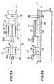
- Figs. 9A and 9Bshow a structure of the n-channel MOSFET circuit 112 formed on a SOI integrated circuit.
- Fig. 9Ais a plan view
- Fig. 9Bis a cross-sectional view taken along the line A-A in Fig. 9A.
- the reference numerals 21, 22, 23, 24 and 25designate the drain, the source, the gate, the body under the gate 23, and the backgate terminal of the high threshold voltage n-channel MOSFET M1, respectively.
- the bodyrefers to the p-region of an n-channel SOI MOSFET or the n-region of a p-channel SOI MOSFET, and corresponds to the backgate region in a-bulk structure.
- the reference numerals 26, 27, 28 and 29designate the source, the drain, the gate, and the body under the gate 28 of the low threshold voltage n-channel MOSFET M2, respectively.
- the reference numerals 30, 31, 32 and 33designate wiring metals, a silicon substrate, a buried oxide and contact holes, respectively.
- the body 24 of the high threshold voltage MOSFET M1is connected to the gate 28 and source 26 of the low threshold voltage MOSFET M2 through the backgate terminal 25 and the wiring metal 30.
- the body 29 of the low threshold voltage MOSFET M2is not connected to its backgate terminal, but is made floating.
- the SOI MOSFETis characterized in that its body can be made floating without providing a well for each MOSFET which is needed in the bulk MOSFET.
- high threshold voltage MOSFETs and low threshold voltage MOSFETscan be fabricated depending on whether the body is biased or not without using a special mask for adjusting the threshold voltage in the fabrication process.
- the threshold voltage of the MOSFETcan be adjusted at higher accuracy by controlling the carrier concentration in the body.
- Fig. 10shows the relationships of the carrier concentration and the threshold voltage. A decrease in the carrier concentration results in an increase in the depletion layer width W, and reduces the voltage needed for forming the channel, thereby reducing the threshold voltage.
- Fig. 11Aillustrates the state in which the carrier concentration is decreased to increase the depletion layer width W so that the body 24A is fully depleted. In this state, the threshold voltage is reduced.
- Fig. 11Billustrates the state in which the carrier concentration is increased to decrease the depletion layer width W so that the body 24B is partially depleted. In this state, the threshold voltage is increased.
- the body 29 of the low threshold voltage MOSFET M2is made fully depleted as shown in Fig. 11A, and the body 24 of the high threshold voltage MOSFET M1 is made partially depleted as shown in Fig. 11B.
- the full depletion layer of the low threshold voltage MOSFET M2results in an increase in its mutual inductance and reduction in the gate capacitance, thereby markedly improving the operating speed.
- Figs. 12A and 12Bshow the n-channel MOSFET 112 as shown in Fig. 6A, which is implemented in a bulk structure.
- the bulk MOSFETincludes an n+ buried layer and a p-well formed in a p-silicon substrate, and backgate regions of the MOSFETs M1 and M2 formed in the p-well.
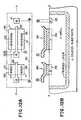
- Figs. 13A - 13Dare diagrams illustrating results of this embodiment.
- Figs. 13A and 13Bshow the circuit arrangement of a conventional MOSFET, and its current characteristics
- Figs. 13C and 13Dshow the circuit arrangement of the MOSFET in accordance with the present invention, and its current characteristics.
- the leakage current I leakincreases exponentially in a conventional n-channel MOSFET Ma whose gate terminal is directly connected to its backgate terminal, because the backgate potential increases in proportion to the supply voltage VDD.
- the circuit in accordance with the present inventioncan reduce the leakage current by four orders in magnitude in comparison with the conventional circuit.
- Fig. 14A and 14Bshow variations ,of the present embodiment.
- the MOSFET of Fig. 14Ais provided with a control terminal besides the gate terminal of the MOSFET of Fig. 6A, and the gate electrode of the MOSFET M1 is connected to the gate terminal.
- the gate of the MOSFET M2is connected to the control terminal.
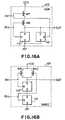
- Figs. 15A and 15Bshow CMOS inverters 122 and 121 including the MOSFET in accordance with the preferred embodiment of the present invention.
- Fig. 15Ashows the CMOS inverter 122 including a low threshold voltage p-channel MOSFET M5 functioning as the load transistor, and the high threshold voltage n-channel MOSFET circuit 112 as shown in Fig. 6A, which functions as the driver transistor.
- Fig. 15Bshows the CMOS inverter 121 including the p-channel MOSFET circuit 111 as shown in Fig. 6B, which functions as the load transistor, and a low threshold voltage n-channel MOSFET M6 functioning as the driver transistor.
- Figs. 16A and 16Bshow variations of the CMOS inverter mentioned above.
- Fig. 16Ashows a 2-input NOR circuit 123
- Fig. 16Bshows a 2-input NAND circuit 124.
- the 2-input NOR circuit 123includes two low threshold voltage p-channel MOSFETs M7 and M8 connected in series to form the load transistor, and the two n-channel MOSFETs 112 as shown in Fig. 6A connected in parallel to form the driver transistor.
- Fig. 16Ashows a 2-input NOR circuit 123
- the 2-input NAND circuit 124includes two low threshold voltage p-channel MOSFETs M9 and M10 connected in parallel to form the load transistor, and the two n-channel MOSFETs 112 as shown in Fig. 6A connected in series to form the driver transistor.
- CMOS structure discussed aboveuses the n-channel MOSFET circuit 112 as shown in Fig. 6A, and the p-channel MOSFET circuit 111 as shown in Fig. 6B, it can realize variable threshold voltage even with the supply voltage VDD > 0.8V by applying the variable bias of the MOSFETs M1 and M2, thereby achieving lower power consumption in a higher supply voltage region.
- the low threshold voltage MOSFETs M5 - M10can be replaced by high threshold voltage MOSFETs in Figs. 15A - 16B.
- Figs. 17, 18A and 18Bshow CMOS logic circuits which are configured using only the MOSFET circuits 111 and 112. as shown in Figs. 6A and 6B.
- Fig. 17shows a CMOS inverter 131 including the n-channel MOSFET circuit 112 functioning as the driver transistor, and the p-channel MOSFET circuit 111 functioning as the load transistor.
- Fig. 18Ashows a 2-input NOR circuit 132 including two p-channel MOSFET circuits 111 connected in series to form the load transistor, and two n-channel MOSFET circuits 112 connected in parallel to form the driver transistors.
- Fig. 17shows a CMOS inverter 131 including the n-channel MOSFET circuit 112 functioning as the driver transistor, and the p-channel MOSFET circuit 111 functioning as the load transistor.
- Fig. 18Ashows a 2-input NOR circuit 132 including two p-channel MOSFET circuits 111 connected in series to form the load transistor
- FIG. 18Bshows a 2-input NAND circuit 133 including two p-channel MOSFET circuits 111 connected in parallel to form the load transistors, and two n-channel MOSFET circuits 112 connected in series to form the driver transistor.
- the p-channel MOSFET circuit 111replaces each of the MOSFETs M7 and M8 of the NOR circuit 123, and the MOSFETs M9 and M10 of the NAND circuit 124 in Figs. 16A and 16B.
- CMOS structure of Figs. 17, 18A, 18Bcan also realize, as the CMOS inverters of Figs. 15A-16B, the variable threshold voltage even for the supply voltage VDD > 0.8V by applying the variable bias of the MOSFETs, thereby achieving the lower power consumption in a higher supply voltage region.
- Figs. 15A - 18Bare characterized in that they can achieve a high speed, low power consumption CMOS logic circuit in a wide power supply voltage.
- Figs. 19A and 19Bshow CMOS logic circuits, in which the CMOS inverter circuit 122 as shown in Fig. 15A and the CMOS inverter circuit 121 as shown in Fig. 15B are alternately connected in cascade to form four stage buffer circuits 141 and 142.
- the buffer circuits 141 and 142differ in that the final stage is the CMOS inverter 121 or 122.
- the low threshold voltage MOSFET M5is off when the input voltage Vin is “H” level, and the output voltage Vout is “L” level.
- the low threshold voltage MOSFET M6is off when the input voltage Vin is "L” level, and the output voltage Vout is “H” level.
- the leakage current of the low threshold voltage MOSFETs M5 and M6is large when they are off because of their insufficient resistance.
- the n-channel MOSFET circuit 112is off when the input voltage Vin is “L” level, and the output voltage Vout is “H” level.
- the p-channel MOSFET circuit 111is off when the input voltage Vin is "H” level, and the output voltage Vout is "L” level. The leakage current of these circuit 112 and 111 is small when they are off because of their sufficiently large resistance.
- the buffer circuit 141 of Fig. 19Ahas a small leakage current because the entire gate circuits have small leakage currents.
- the static current of the buffer circuit 141is small when the input voltage is "H", but is large when the input voltage is "L".
- the buffer circuit 142 of Fig. 19Bhas a small leakage current when the input and output terminals are placed at "L" level because the entire gate circuits have small leakage currents.
- the static current of the buffer circuit 142is small when the input voltage is "L", but is large when the input voltage is "H”.
- Figs. 20, 21A and 21Bare circuit diagrams showing an alternative configuration.
- Fig. 20shows a CMOS logic circuit 151 in which the p-channel MOSFET 111 circuit shown in Fig. 6B replaces the high-potential power supply controller 4 in the CMOS logic circuit described with reference to Fig. 2, and the n-channel MOSFET circuit 112 shown in Fig. 6A replaces the low-potential power supply controller 5.
- VDD0.8V
- the backgate voltage of the high threshold voltage MOSFETs M1 and M3are clamped by the low threshold voltage MOSFETs M2 and M4 in the MOSFET circuits 112 and 111. Therefore, the increase in the gate current is prevented, and the threshold voltage during the operation is dropped, thereby achieving the low impedance of the MOSFETs M1 and M3, and implementing the high speed operation.
- the advantages of the circuit as shown in Fig. 2are achieved to a wider supply voltage range.
- CMOS logic circuit 152as shown in Fig. 21A can be implemented in which only the p-channel MOSFET circuit 111 is connected to the high-potential side
- CMOS logic circuit 153as shown in Fig. 21B can be implemented in which only the n-channel MOSFET circuit 112 is connected to the low-potential side.
- the power supply terminal to which the power supply controller is not connectedis directly connected to the power supply VDD or to the ground.
- Figs. 22A - 22Care circuit diagrams showing a sixth embodiment further alternative configuration.
- Fig. 22Ashows a configuration in which the buffer circuits 141 and 142 as shown in Figs. 19A and 19B are connected to the input terminals of the signals SL and *SL of the CMOS logic circuit 151 shown in Fig. 20, respectively.
- Fig. 22Bshows a configuration in which the buffer circuits 141 as shown in Fig. 19A is connected to the input terminal of the signal SL of the CMOS logic circuit 152 shown in Fig. 21A
- Fig. 22Cshows a configuration in which the buffer circuits 142 as shown in Fig. 19B is connected to the input terminal of the signal *SL of the CMOS logic circuit 153 shown in Fig. 21B.
- the rest current of the buffer circuits 141 and 142decreases when the signal SL is "H” and the signal *SL is "L", that is, when the low threshold voltage CMOS logic circuit group 3 is in a waiting (sleeping) mode.
- the circuits as shown in Fig. 22A - 22Chave an advantage that they can achieve the high speed operation in the active mode and the low power consumption in the waiting mode at the same time in a wide supply voltage range from less than 1V up to 3 to 5V.
- the arrangements as shown in Figs. 20 - 22Ccan implement a high speed, low power consumption multi-threshold CMOS logic circuit in a wide supply voltage.
- the configurations in Figs. 22A - 22Chas a very low leakage current, and hence very low power consumption in the waiting mode, and is effective when the waiting mode is longer than the active mode.
- the potential of the bodywill increase (decrease) owing to the inflow of holes (electrons) from the drain to the body.
- the threshold voltagedrops, and the MOSFETs in the CMOS logic circuit can operate at a low voltage.
- Fig. 23is a circuit diagram showing another MOSFET circuit.
- the reference numeral 201designates a first control terminal to which a control signal C is input
- 202denotes a second control terminal to which a control signal *C complementary to the control signal C is input
- 203designates an internal CMOS circuit including n-cascaded CMOS inverters
- 204denotes a signal input terminal
- 205denotes a signal output terminal.
- all the backgate terminals of p-channel MOSFETs M31 - M3n constituting the load MOSFETs of the internal CMOS circuit 203are connected to the first control terminal 201 through a p-channel MOSFET M1 (a first rectifier element) whose gate and source are interconnected.
- all the backgate terminals of n-channel MOSFETs M41 - M4n constituting the driver MOSFETs of the internal CMOS circuit 203are connected to the second control terminal 202 through an n-channel MOSFET M2 (a second rectifier element) whose gate and source are interconnected.
- the p-channel MOSFET M1with its gate and source interconnected conducts a forward current from the drain to the gate and source, thereby functioning as a diode whose anode is the drain, and cathode is the gate and source.
- the forward voltage Vf of the diodeis the threshold voltage of the MOSFET M1.
- the n-channel MOSFET M2with its gate and source interconnected conducts a forward current from the gate and source to the drain, thereby functioning as a diode whose anode is the gate and source, and cathode is the drain.
- the forward voltage Vf of the diodeis the threshold voltage of the MOSFET M2.
- the n-channel MOSFET M2 functioning as a rectifier elementis also reversely biased, and operates as one of the reference diodes due to its leakage current. This will increase the backgate voltage of the MOSFETs M41 - M4n, thereby reducing their threshold voltage.
- the drop of the threshold voltagesmakes it possible for MOSFETs to operated at a high speed even with a low supply voltage near the original threshold voltage of the MOSFETs.
- the reverse-biased MOSFETs M1 and M2through which only the leakage current flows, can prevent short-circuit current from flowing. This effect is particularly distinct when the supply voltage exceeds the forward voltage Vf (0.8V) of the diode D3, in comparison with the conventional circuit.
- the small leakage current flowing through the rectifier MOSFETs M1 and M2can prevent a great decrease in the backgate potential of the p-channel MOSFETs M31 - M3n, and a great increase in the backgate potential of the n-channel MOSFETs M41 - M4n.
- the rectifier MOSFETs M1 and M2are forwardly biased. This will set the backgate terminals of the p-channel MOSFETs M31 - M3n at a high potential, and the backgate terminals of the n-channel MOSFETs M41 - M4n at a low potential.
- the source terminal and backgate terminal of each of the MOSFETs M31 - M3n and M41 - M4nare kept equipotential, thereby causing no drop in the threshold voltage or short-circuit current.
- the circuitis in an active mode when the control signal C is low, and the control signal *C is high, because the threshold voltage of the MOSFETs is changed low in this case. Accordingly, it is possible for the circuit to use a low supply voltage, and to achieve a high speed operation in the active mode.
- the circuitis in a sleep mode when the control signal C is high, and the control signal *C is low, in which case the threshold voltage of the MOSFETs is kept at the original high threshold voltage. Accordingly, it is possible for the circuit to reduce the power consumption in the sleep mode because the leakage current flowing through the source and drain of each of the MOSFETs is kept very low in this mode.
- the rectifier p-channel MOSFET M1is common to all the p-channel MOSFETs M31 - M3n
- the rectifier n-channel MOSFET M2is common to all the n-channel MOSFETs M41 - M4n in the internal CMOS circuit 203 in Fig. 23, this is not essential.
- the rectifier MOSFETcan be connected to each one of the MOSFETs, or to each set of plurality of MOSFETs in the internal CMOS circuit 203.
- the rectifier MOSFETsare connected to the backgate terminals of both the p-channel MOSFETs M31 - M3n and n-channel MOSFETs M41 and M4n in the internal CMOS circuit 203, this is not necessary.
- the rectifier MOSFETcan be connected to the backgate terminals of either the p- or n-channel MOSFETs, and a fixed voltage can be connected to the backgate terminals of the remaining MOSFETs.
- the backgate terminals of the remaining MOSFETscan be made floating. In this case, the complementary control signal *C is not needed.
- CMOS circuit 203consists of the CMOS inverters connected in cascade in Fig. 23, it can include CMOS circuits other than CMOS inverters.
- Fig. 25is a circuit diagram of another MOSFET circuit.
- a p-channel MOSFET M5 and an n-channel MOSFET M6are used as a rectifier transistor with its gate and source connected in common.
- Each of these MOSFETsis a low threshold voltage MOSFET with a threshold voltage lower than that of the MOSFETs M31 - M3n and M41 - M4n constituting the internal CMOS circuit 203.
- the MOSFETs M31 - M3n and M41 - M4nhave a threshold voltage of 0.6V
- the rectifier MOSFETs M5 and M6have a threshold voltage of 0.2V.
- Using such a low threshold voltage MOSFETs as the rectifier MOSFETs M5 and M6has an advantage that a desired leakage current can be achieved with a small area. This is because a low threshold voltage MOSFET has a large leakage current.
- Fig. 26is circuit diagram showing still another MOSFET circuit.
- the internal circuit 203 of this circuitis a latch circuit 206 including two cascaded inverters and a transmission gate connected in a loop.
- the two invertersare each arranged by combining a p-channel MOSFET M31 with an n-channel MOSFET M41, and M32 with M42, and the transmission gate is composed of a p-channel MOSFET M33 and an n-channel MOSFET M43.
- the backgate terminals of the p-channel MOSFETs M31 - M33 of the latch circuit 206is connected to a first control terminal 201 through a rectifier MOSFET M5, and the backgate terminals of the n-channel MOSFETs M41 and M43 are connected to a second control terminal 202 through a rectifier MOSFET M6.
- the threshold voltageschange of the p-channel MOSFET M33 and the n-channel MOSFET M43 constituting the transmission gate:
- the threshold voltagesare lower when they are in a conductive state than in a non-conductive state. This reduces the ON state resistance of the transmission gate, thereby ensuring its memory operation with a low supply voltage just above the threshold voltage of the non-conductive MOSFETs M33 and M43.
- Fig. 27is a circuit diagram of a last MOSFET circuit.
- the internal CMOS circuit 203is a memory cell 207 composed of p-channel MOSFETs M71 and M72, n-channel MOSFETs M81 and M82, and n-channel MOSFETs M91 and M92 constituting transmission gates.
- the backgate terminals of the n-channel MOSFETs M81, M82, M91 and M92are connected to a control word line 209 which is connected to a word line 208 through a rectifier n-channel MOSFET M10.
- the reference numeral 210designates a bit line, and 211 denotes an inverted bit line.
- the threshold voltagewill drop of the n-channel MOSFETs of the memory cell 207 selected by the word line 208, thereby reducing an equivalent resistance of these MOSFETs. This enables the memory cell 207 to read and write positively even with a low supply voltage at which the ON state resistance of the MOSFETs increases.
- the transmission gates of the memory cell 207employ the n-channel MOSFETs M91 and M92 in the configuration of Fig. 27, it can use p-channel MOSFETs with their backgate terminals connected to the word line 208 through a rectifier MOSFET. Furthermore, complementary control words can also be adopted, in which case the circuit becomes similar to those of Figs. 23 and 25.
- Fig. 28is a graph illustrating a reduction effect of the leakage current I leak flowing through the backgate terminal and the source terminal of a MOSFET when they are forwardly biased. As is clear from this figure, the leakage current I leak is greatly reduced in the MOSFET in accordance with the present invention.
- each MOSFET formed on the SOI substratehas an independent backgate region, and hence the potential of the backgate terminal can be set rather arbitrary.
Landscapes
- Physics & Mathematics (AREA)
- Engineering & Computer Science (AREA)
- Computer Hardware Design (AREA)
- Computing Systems (AREA)
- General Engineering & Computer Science (AREA)
- Mathematical Physics (AREA)
- Logic Circuits (AREA)
Description
Claims (2)
- A MOSFET circuit (111, 112)characterised bycomprising:wherein a leakage current through said second MOSFET limits a forward currentof a parasitic diode between a source electrode and thebackgate electrode of said first MOSFET.a first MOSFET (M1, M3) having a first thresholdvoltage; anda second MOSFET (M2, M4) having a second thresholdvoltage lower than or equal to said first thresholdvoltage, said second MOSFET (M2, M4) having a gateelectrode (G), and a source electrode (S)connected to a backgate electrode (B) of said firstMOSFET (M1, M3), and a drain electrode (D)connected to an external signal (G);
- The MOSFET circuit as claimed in claim 1,characterised in that a gate electrode of said firstMOSFET (M1, M3) is connected to the drainelectrode (D) of said second MOSFET (M2, M4).
Applications Claiming Priority (6)
| Application Number | Priority Date | Filing Date | Title |
|---|---|---|---|
| JP120902/95 | 1995-04-21 | ||
| JP12090295 | 1995-04-21 | ||
| JP12090295 | 1995-04-21 | ||
| JP23211295 | 1995-08-18 | ||
| JP232112/95 | 1995-08-18 | ||
| JP23211295 | 1995-08-18 |
Publications (3)
| Publication Number | Publication Date |
|---|---|
| EP0739097A2 EP0739097A2 (en) | 1996-10-23 |
| EP0739097A3 EP0739097A3 (en) | 1998-01-07 |
| EP0739097B1true EP0739097B1 (en) | 2004-04-07 |
Family
ID=26458395
Family Applications (1)
| Application Number | Title | Priority Date | Filing Date |
|---|---|---|---|
| EP96106128AExpired - LifetimeEP0739097B1 (en) | 1995-04-21 | 1996-04-18 | MOSFET circuit and CMOS logic circuit using the same |
Country Status (3)
| Country | Link |
|---|---|
| US (1) | US5821769A (en) |
| EP (1) | EP0739097B1 (en) |
| DE (1) | DE69632098T2 (en) |
Cited By (48)
| Publication number | Priority date | Publication date | Assignee | Title |
|---|---|---|---|---|
| US7251164B2 (en) | 2004-11-10 | 2007-07-31 | Innovative Silicon S.A. | Circuitry for and method of improving statistical distribution of integrated circuits |
| US7301803B2 (en) | 2004-12-22 | 2007-11-27 | Innovative Silicon S.A. | Bipolar reading technique for a memory cell having an electrically floating body transistor |
| US7301838B2 (en) | 2004-12-13 | 2007-11-27 | Innovative Silicon S.A. | Sense amplifier circuitry and architecture to write data into and/or read from memory cells |
| US7355916B2 (en) | 2005-09-19 | 2008-04-08 | Innovative Silicon S.A. | Method and circuitry to generate a reference current for reading a memory cell, and device implementing same |
| US7359229B2 (en) | 2003-05-13 | 2008-04-15 | Innovative Silicon S.A. | Semiconductor memory device and method of operating same |
| US7476939B2 (en) | 2004-11-04 | 2009-01-13 | Innovative Silicon Isi Sa | Memory cell having an electrically floating body transistor and programming technique therefor |
| US7492632B2 (en) | 2006-04-07 | 2009-02-17 | Innovative Silicon Isi Sa | Memory array having a programmable word length, and method of operating same |
| US7542345B2 (en) | 2006-02-16 | 2009-06-02 | Innovative Silicon Isi Sa | Multi-bit memory cell having electrically floating body transistor, and method of programming and reading same |
| US7542340B2 (en) | 2006-07-11 | 2009-06-02 | Innovative Silicon Isi Sa | Integrated circuit including memory array having a segmented bit line architecture and method of controlling and/or operating same |
| US7606098B2 (en) | 2006-04-18 | 2009-10-20 | Innovative Silicon Isi Sa | Semiconductor memory array architecture with grouped memory cells, and method of controlling same |
| US7606066B2 (en) | 2005-09-07 | 2009-10-20 | Innovative Silicon Isi Sa | Memory cell and memory cell array having an electrically floating body transistor, and methods of operating same |
| US7683430B2 (en) | 2005-12-19 | 2010-03-23 | Innovative Silicon Isi Sa | Electrically floating body memory cell and array, and method of operating or controlling same |
| US7924630B2 (en) | 2008-10-15 | 2011-04-12 | Micron Technology, Inc. | Techniques for simultaneously driving a plurality of source lines |
| US7933140B2 (en) | 2008-10-02 | 2011-04-26 | Micron Technology, Inc. | Techniques for reducing a voltage swing |
| US7933142B2 (en) | 2006-05-02 | 2011-04-26 | Micron Technology, Inc. | Semiconductor memory cell and array using punch-through to program and read same |
| US7947543B2 (en) | 2008-09-25 | 2011-05-24 | Micron Technology, Inc. | Recessed gate silicon-on-insulator floating body device with self-aligned lateral isolation |
| US7957206B2 (en) | 2008-04-04 | 2011-06-07 | Micron Technology, Inc. | Read circuitry for an integrated circuit having memory cells and/or a memory cell array, and method of operating same |
| US8014195B2 (en) | 2008-02-06 | 2011-09-06 | Micron Technology, Inc. | Single transistor memory cell |
| US8064274B2 (en) | 2007-05-30 | 2011-11-22 | Micron Technology, Inc. | Integrated circuit having voltage generation circuitry for memory cell array, and method of operating and/or controlling same |
| US8069377B2 (en) | 2006-06-26 | 2011-11-29 | Micron Technology, Inc. | Integrated circuit having memory array including ECC and column redundancy and method of operating the same |
| US8085594B2 (en) | 2007-06-01 | 2011-12-27 | Micron Technology, Inc. | Reading technique for memory cell with electrically floating body transistor |
| US8139418B2 (en) | 2009-04-27 | 2012-03-20 | Micron Technology, Inc. | Techniques for controlling a direct injection semiconductor memory device |
| US8174881B2 (en) | 2009-11-24 | 2012-05-08 | Micron Technology, Inc. | Techniques for reducing disturbance in a semiconductor device |
| US8189376B2 (en) | 2008-02-08 | 2012-05-29 | Micron Technology, Inc. | Integrated circuit having memory cells including gate material having high work function, and method of manufacturing same |
| US8194487B2 (en) | 2007-09-17 | 2012-06-05 | Micron Technology, Inc. | Refreshing data of memory cells with electrically floating body transistors |
| US8199595B2 (en) | 2009-09-04 | 2012-06-12 | Micron Technology, Inc. | Techniques for sensing a semiconductor memory device |
| US8213226B2 (en) | 2008-12-05 | 2012-07-03 | Micron Technology, Inc. | Vertical transistor memory cell and array |
| US8223574B2 (en) | 2008-11-05 | 2012-07-17 | Micron Technology, Inc. | Techniques for block refreshing a semiconductor memory device |
| US8264041B2 (en) | 2007-01-26 | 2012-09-11 | Micron Technology, Inc. | Semiconductor device with electrically floating body |
| US8310893B2 (en) | 2009-12-16 | 2012-11-13 | Micron Technology, Inc. | Techniques for reducing impact of array disturbs in a semiconductor memory device |
| US8315099B2 (en) | 2009-07-27 | 2012-11-20 | Micron Technology, Inc. | Techniques for providing a direct injection semiconductor memory device |
| US8319294B2 (en) | 2009-02-18 | 2012-11-27 | Micron Technology, Inc. | Techniques for providing a source line plane |
| US8349662B2 (en) | 2007-12-11 | 2013-01-08 | Micron Technology, Inc. | Integrated circuit having memory cell array, and method of manufacturing same |
| US8369177B2 (en) | 2010-03-05 | 2013-02-05 | Micron Technology, Inc. | Techniques for reading from and/or writing to a semiconductor memory device |
| US8411524B2 (en) | 2010-05-06 | 2013-04-02 | Micron Technology, Inc. | Techniques for refreshing a semiconductor memory device |
| US8411513B2 (en) | 2010-03-04 | 2013-04-02 | Micron Technology, Inc. | Techniques for providing a semiconductor memory device having hierarchical bit lines |
| US8416636B2 (en) | 2010-02-12 | 2013-04-09 | Micron Technology, Inc. | Techniques for controlling a semiconductor memory device |
| US8498157B2 (en) | 2009-05-22 | 2013-07-30 | Micron Technology, Inc. | Techniques for providing a direct injection semiconductor memory device |
| US8508994B2 (en) | 2009-04-30 | 2013-08-13 | Micron Technology, Inc. | Semiconductor device with floating gate and electrically floating body |
| US8518774B2 (en) | 2007-03-29 | 2013-08-27 | Micron Technology, Inc. | Manufacturing process for zero-capacitor random access memory circuits |
| US8531878B2 (en) | 2011-05-17 | 2013-09-10 | Micron Technology, Inc. | Techniques for providing a semiconductor memory device |
| US8536628B2 (en) | 2007-11-29 | 2013-09-17 | Micron Technology, Inc. | Integrated circuit having memory cell array including barriers, and method of manufacturing same |
| US8537610B2 (en) | 2009-07-10 | 2013-09-17 | Micron Technology, Inc. | Techniques for providing a semiconductor memory device |
| US8547738B2 (en) | 2010-03-15 | 2013-10-01 | Micron Technology, Inc. | Techniques for providing a semiconductor memory device |
| US8576631B2 (en) | 2010-03-04 | 2013-11-05 | Micron Technology, Inc. | Techniques for sensing a semiconductor memory device |
| US8710566B2 (en) | 2009-03-04 | 2014-04-29 | Micron Technology, Inc. | Techniques for forming a contact to a buried diffusion layer in a semiconductor memory device |
| US8748959B2 (en) | 2009-03-31 | 2014-06-10 | Micron Technology, Inc. | Semiconductor memory device |
| US9559216B2 (en) | 2011-06-06 | 2017-01-31 | Micron Technology, Inc. | Semiconductor memory device and method for biasing same |
Families Citing this family (126)
| Publication number | Priority date | Publication date | Assignee | Title |
|---|---|---|---|---|
| KR0150750B1 (en)* | 1995-05-19 | 1998-10-01 | 김주용 | Reduced power consumption semiconductor circuit in the stand-by state |
| DE69730775T2 (en)* | 1996-05-22 | 2005-09-29 | Nippon Telegraph And Telephone Corp. | Logic circuit and related manufacturing process |
| JP3195256B2 (en)* | 1996-10-24 | 2001-08-06 | 株式会社東芝 | Semiconductor integrated circuit |
| JP3451579B2 (en)* | 1997-03-03 | 2003-09-29 | 日本電信電話株式会社 | Self-synchronous pipeline data path circuit |
| JP3715066B2 (en)* | 1997-03-25 | 2005-11-09 | 三菱電機株式会社 | Current mode logic circuit |
| JP3178799B2 (en)* | 1997-04-18 | 2001-06-25 | シャープ株式会社 | MOS logic circuit and semiconductor device provided with the MOS logic circuit |
| US5939899A (en)* | 1997-04-23 | 1999-08-17 | Lucent Technologies Inc. | MOSFET substrate current logic |
| EP0875991A1 (en)* | 1997-04-25 | 1998-11-04 | Philips Patentverwaltung GmbH | Circuit arrangement for generating an electronically controlled resistor |
| US6593799B2 (en) | 1997-06-20 | 2003-07-15 | Intel Corporation | Circuit including forward body bias from supply voltage and ground nodes |
| CN1196263C (en)* | 1997-06-20 | 2005-04-06 | 英特尔公司 | Forward body bias transistor circuit |
| DE19738714A1 (en)* | 1997-09-04 | 1999-03-18 | Siemens Ag | Integrated circuit with a switching transistor |
| KR100269643B1 (en)* | 1997-11-27 | 2000-10-16 | 김영환 | Power reduction circuit |
| JP3542476B2 (en) | 1997-12-01 | 2004-07-14 | 三菱電機株式会社 | CMOS circuit with SOI structure |
| US6308312B1 (en)* | 1997-12-19 | 2001-10-23 | Texas Instruments Incorporated | System and method for controlling leakage current in an integrated circuit using current limiting devices |
| US6104213A (en)* | 1998-03-02 | 2000-08-15 | International Business Machines Corporation | Domino logic circuit having a clocked precharge |
| JPH11330918A (en) | 1998-05-20 | 1999-11-30 | Nec Corp | Sequential circuit |
| JPH11355123A (en)* | 1998-06-11 | 1999-12-24 | Mitsubishi Electric Corp | Buffer using dynamic threshold MOS transistor |
| JP3499748B2 (en) | 1998-06-12 | 2004-02-23 | Necエレクトロニクス株式会社 | Sequential circuit |
| JP3947308B2 (en)* | 1998-06-17 | 2007-07-18 | 沖電気工業株式会社 | Semiconductor integrated circuit |
| US6097243A (en)* | 1998-07-21 | 2000-08-01 | International Business Machines Corporation | Device and method to reduce power consumption in integrated semiconductor devices using a low power groggy mode |
| JP3519001B2 (en)* | 1998-10-15 | 2004-04-12 | シャープ株式会社 | Latch circuit and flip-flop circuit |
| US6150834A (en)* | 1998-11-12 | 2000-11-21 | International Business Machines Corporation | Elimination of SOI parasitic bipolar effect |
| KR100451495B1 (en)* | 1998-12-12 | 2004-12-31 | 주식회사 하이닉스반도체 | Semiconductor Integrated Circuits with Standby Current Reduction Circuits |
| US6826730B2 (en) | 1998-12-15 | 2004-11-30 | Texas Instruments Incorporated | System and method for controlling current in an integrated circuit |
| FR2789519B1 (en)* | 1999-02-05 | 2003-03-28 | Commissariat Energie Atomique | MOS TRANSISTOR WITH A DYNAMIC THRESHOLD VOLTAGE EQUIPPED WITH A CURRENT LIMITER, AND METHOD OF MAKING SUCH A TRANSISTOR |
| US6111778A (en)* | 1999-05-10 | 2000-08-29 | International Business Machines Corporation | Body contacted dynamic memory |
| US6275094B1 (en) | 1999-06-22 | 2001-08-14 | International Business Machines Corporation | CMOS device and circuit and method of operation dynamically controlling threshold voltage |
| JP2001036388A (en)* | 1999-07-16 | 2001-02-09 | Sharp Corp | Level shift circuit and semiconductor device |
| DE10010886C1 (en)* | 2000-03-06 | 2002-01-17 | Infineon Technologies Ag | Sense amplifier subcircuit for a DRAM memory and corresponding DRAM memory |
| US6433587B1 (en) | 2000-03-17 | 2002-08-13 | International Business Machines Corporation | SOI CMOS dynamic circuits having threshold voltage control |
| JP3523611B2 (en)* | 2000-05-31 | 2004-04-26 | 日本電信電話株式会社 | Differential logic circuit |
| US6537891B1 (en) | 2000-08-29 | 2003-03-25 | Micron Technology, Inc. | Silicon on insulator DRAM process utilizing both fully and partially depleted devices |
| US6633197B1 (en) | 2000-10-27 | 2003-10-14 | Marvell International, Ltd. | Gate capacitor stress reduction in CMOS/BICMOS circuit |
| US6744301B1 (en)* | 2000-11-07 | 2004-06-01 | Intel Corporation | System using body-biased sleep transistors to reduce leakage power while minimizing performance penalties and noise |
| US6605981B2 (en)* | 2001-04-26 | 2003-08-12 | International Business Machines Corporation | Apparatus for biasing ultra-low voltage logic circuits |
| TWI230392B (en) | 2001-06-18 | 2005-04-01 | Innovative Silicon Sa | Semiconductor device |
| US6677802B2 (en)* | 2001-09-05 | 2004-01-13 | International Business Machines Corporation | Method and apparatus for biasing body voltages |
| US6804502B2 (en) | 2001-10-10 | 2004-10-12 | Peregrine Semiconductor Corporation | Switch circuit and method of switching radio frequency signals |
| JP3740577B2 (en) | 2001-12-20 | 2006-02-01 | 松下電器産業株式会社 | Negative potential generating circuit, negative potential generating device, and semiconductor device using the same |
| JP3865689B2 (en) | 2002-01-15 | 2007-01-10 | 松下電器産業株式会社 | Level shift circuit |
| EP1355316B1 (en) | 2002-04-18 | 2007-02-21 | Innovative Silicon SA | Data storage device and refreshing method for use with such device |
| EP1357603A3 (en) | 2002-04-18 | 2004-01-14 | Innovative Silicon SA | Semiconductor device |
| JP3928937B2 (en)* | 2002-05-24 | 2007-06-13 | シャープ株式会社 | Semiconductor integrated circuit |
| US6933744B2 (en)* | 2002-06-11 | 2005-08-23 | The Regents Of The University Of Michigan | Low-leakage integrated circuits and dynamic logic circuits |
| JP2004111826A (en)* | 2002-09-20 | 2004-04-08 | Renesas Technology Corp | Semiconductor device and method of manufacturing the same |
| JP2004336010A (en)* | 2003-04-16 | 2004-11-25 | Seiko Epson Corp | Semiconductor integrated circuit, electronic device, and method of controlling back gate potential of transistor |
| US7085153B2 (en) | 2003-05-13 | 2006-08-01 | Innovative Silicon S.A. | Semiconductor memory cell, array, architecture and device, and method of operating same |
| US6912150B2 (en) | 2003-05-13 | 2005-06-28 | Lionel Portman | Reference current generator, and method of programming, adjusting and/or operating same |
| US7335934B2 (en) | 2003-07-22 | 2008-02-26 | Innovative Silicon S.A. | Integrated circuit device, and method of fabricating same |
| US7184298B2 (en) | 2003-09-24 | 2007-02-27 | Innovative Silicon S.A. | Low power programming technique for a floating body memory transistor, memory cell, and memory array |
| KR100585886B1 (en)* | 2004-01-27 | 2006-06-01 | 삼성전자주식회사 | Semiconductor circuit with dynamic threshold voltage |
| EP3570374B1 (en) | 2004-06-23 | 2022-04-20 | pSemi Corporation | Integrated rf front end |
| US8247840B2 (en)* | 2004-07-07 | 2012-08-21 | Semi Solutions, Llc | Apparatus and method for improved leakage current of silicon on insulator transistors using a forward biased diode |
| US7375402B2 (en)* | 2004-07-07 | 2008-05-20 | Semi Solutions, Llc | Method and apparatus for increasing stability of MOS memory cells |
| US7224205B2 (en)* | 2004-07-07 | 2007-05-29 | Semi Solutions, Llc | Apparatus and method for improving drive-strength and leakage of deep submicron MOS transistors |
| US7683433B2 (en)* | 2004-07-07 | 2010-03-23 | Semi Solution, Llc | Apparatus and method for improving drive-strength and leakage of deep submicron MOS transistors |
| US7319357B2 (en)* | 2004-08-24 | 2008-01-15 | Texas Instruments Incorporated | System for controlling switch transistor performance |
| EP1831932B1 (en)* | 2004-12-29 | 2013-05-08 | Semi Solutions LLC. | Apparatus and method for improving drive strength, leakage and stability of deep submicron mos transistors and memory cells |
| US7651905B2 (en)* | 2005-01-12 | 2010-01-26 | Semi Solutions, Llc | Apparatus and method for reducing gate leakage in deep sub-micron MOS transistors using semi-rectifying contacts |
| US7898297B2 (en)* | 2005-01-04 | 2011-03-01 | Semi Solution, Llc | Method and apparatus for dynamic threshold voltage control of MOS transistors in dynamic logic circuits |
| KR100699832B1 (en)* | 2005-01-05 | 2007-03-27 | 삼성전자주식회사 | MTCMCOS control circuit |
| JP4291295B2 (en)* | 2005-04-08 | 2009-07-08 | エルピーダメモリ株式会社 | Logic circuit |
| US7084462B1 (en)* | 2005-04-15 | 2006-08-01 | International Business Machines Corporation | Parallel field effect transistor structure having a body contact |
| USRE48965E1 (en) | 2005-07-11 | 2022-03-08 | Psemi Corporation | Method and apparatus improving gate oxide reliability by controlling accumulated charge |
| US8742502B2 (en) | 2005-07-11 | 2014-06-03 | Peregrine Semiconductor Corporation | Method and apparatus for use in improving linearity of MOSFETs using an accumulated charge sink-harmonic wrinkle reduction |
| US20080076371A1 (en) | 2005-07-11 | 2008-03-27 | Alexander Dribinsky | Circuit and method for controlling charge injection in radio frequency switches |
| US7890891B2 (en) | 2005-07-11 | 2011-02-15 | Peregrine Semiconductor Corporation | Method and apparatus improving gate oxide reliability by controlling accumulated charge |
| US7910993B2 (en) | 2005-07-11 | 2011-03-22 | Peregrine Semiconductor Corporation | Method and apparatus for use in improving linearity of MOSFET's using an accumulated charge sink |
| US9653601B2 (en) | 2005-07-11 | 2017-05-16 | Peregrine Semiconductor Corporation | Method and apparatus for use in improving linearity of MOSFETs using an accumulated charge sink-harmonic wrinkle reduction |
| TW200707177A (en)* | 2005-08-08 | 2007-02-16 | Ind Tech Res Inst | Leakage current control circuit with a single low voltage power supply and method thereof |
| US7250656B2 (en)* | 2005-08-19 | 2007-07-31 | International Business Machines Corporation | Hybrid-orientation technology buried n-well design |
| US20070047364A1 (en)* | 2005-08-31 | 2007-03-01 | International Business Machines Corporation | Methods and apparatus for varying a supply voltage or reference voltage using independent control of diode voltage in asymmetrical double-gate devices |
| JP5105462B2 (en)* | 2005-12-27 | 2012-12-26 | ルネサスエレクトロニクス株式会社 | Semiconductor integrated circuit |
| JP2007201236A (en)* | 2006-01-27 | 2007-08-09 | Renesas Technology Corp | Semiconductor integrated circuit |
| JP2007208004A (en)* | 2006-02-01 | 2007-08-16 | Matsushita Electric Ind Co Ltd | Semiconductor integrated circuit device and electronic device |
| US7863689B2 (en)* | 2006-09-19 | 2011-01-04 | Semi Solutions, Llc. | Apparatus for using a well current source to effect a dynamic threshold voltage of a MOS transistor |
| US7864492B2 (en)* | 2006-10-31 | 2011-01-04 | Siemens Industry, Inc. | Systems and methods for arc fault detection |
| WO2008114379A1 (en)* | 2007-03-19 | 2008-09-25 | Fujitsu Limited | Inverter circuit and balanced input inverter circuit |
| US8587062B2 (en)* | 2007-03-26 | 2013-11-19 | International Business Machines Corporation | Silicon on insulator (SOI) field effect transistors (FETs) with adjacent body contacts |
| US20080290413A1 (en)* | 2007-05-21 | 2008-11-27 | International Business Machines Corporation | Soi mosfet with a metal semiconductor alloy gate-to-body bridge |
| WO2009046114A2 (en)* | 2007-10-01 | 2009-04-09 | University Of Florida Research Foundation, Inc. | Two-transistor floating-body dynamic memory cell |
| TWI345690B (en)* | 2007-10-05 | 2011-07-21 | Ind Tech Res Inst | System on a chip and power gating circuit thereof |
| US8773933B2 (en) | 2012-03-16 | 2014-07-08 | Micron Technology, Inc. | Techniques for accessing memory cells |
| US8207784B2 (en)* | 2008-02-12 | 2012-06-26 | Semi Solutions, Llc | Method and apparatus for MOSFET drain-source leakage reduction |
| US9024700B2 (en)* | 2008-02-28 | 2015-05-05 | Peregrine Semiconductor Corporation | Method and apparatus for use in digitally tuning a capacitor in an integrated circuit device |
| US7924087B2 (en)* | 2008-05-20 | 2011-04-12 | Mediatek Inc. | Reference buffer circuit |
| US9824008B2 (en)* | 2008-11-21 | 2017-11-21 | International Business Machines Corporation | Cache memory sharing in a multi-core processor (MCP) |
| US9122617B2 (en)* | 2008-11-21 | 2015-09-01 | International Business Machines Corporation | Pseudo cache memory in a multi-core processor (MCP) |
| US7804329B2 (en)* | 2008-11-21 | 2010-09-28 | International Business Machines Corporation | Internal charge transfer for circuits |
| US8806129B2 (en)* | 2008-11-21 | 2014-08-12 | International Business Machines Corporation | Mounted cache memory in a multi-core processor (MCP) |
| US9886389B2 (en) | 2008-11-21 | 2018-02-06 | International Business Machines Corporation | Cache memory bypass in a multi-core processor (MCP) |
| US8319548B2 (en)* | 2009-02-18 | 2012-11-27 | Freescale Semiconductor, Inc. | Integrated circuit having low power mode voltage regulator |
| US20100283445A1 (en)* | 2009-02-18 | 2010-11-11 | Freescale Semiconductor, Inc. | Integrated circuit having low power mode voltage regulator |
| US8723260B1 (en) | 2009-03-12 | 2014-05-13 | Rf Micro Devices, Inc. | Semiconductor radio frequency switch with body contact |
| JP5372578B2 (en) | 2009-04-09 | 2013-12-18 | ルネサスエレクトロニクス株式会社 | Semiconductor device |
| US8193616B2 (en)* | 2009-06-29 | 2012-06-05 | Kabushiki Kaisha Toshiba | Semiconductor device on direct silicon bonded substrate with different layer thickness |
| JP5031809B2 (en)* | 2009-11-13 | 2012-09-26 | ユニサンティス エレクトロニクス シンガポール プライベート リミテッド | Semiconductor device |
| US8400819B2 (en)* | 2010-02-26 | 2013-03-19 | Freescale Semiconductor, Inc. | Integrated circuit having variable memory array power supply voltage |
| US8456140B2 (en) | 2010-07-14 | 2013-06-04 | Arm Limited | Power control apparatus and method for controlling a supply voltage for an associated circuit |
| FR2964794A1 (en)* | 2010-09-14 | 2012-03-16 | St Microelectronics Sa | DYNAMIC POLARIZATION CIRCUIT OF THE SUBSTRATE OF A TRANSISTOR |
| WO2012112594A2 (en)* | 2011-02-14 | 2012-08-23 | California Institute Of Technology | Systems and methods for dynamic mosfet body biasing for low power, fast response vlsi applications |
| US9035629B2 (en) | 2011-04-29 | 2015-05-19 | Freescale Semiconductor, Inc. | Voltage regulator with different inverting gain stages |
| CN103000221B (en)* | 2011-09-09 | 2016-01-20 | 华邦电子股份有限公司 | Semiconductor device |
| TWI494673B (en)* | 2012-09-21 | 2015-08-01 | Innocom Tech Shenzhen Co Ltd | Display device |
| WO2014047823A1 (en)* | 2012-09-27 | 2014-04-03 | Qualcomm Incorporated | Power switch cell with adaptive body bias |
| US8975952B2 (en)* | 2012-11-13 | 2015-03-10 | Honeywell International Inc. | CMOS logic circuit using passive internal body tie bias |
| US9590674B2 (en) | 2012-12-14 | 2017-03-07 | Peregrine Semiconductor Corporation | Semiconductor devices with switchable ground-body connection |
| US20150236748A1 (en) | 2013-03-14 | 2015-08-20 | Peregrine Semiconductor Corporation | Devices and Methods for Duplexer Loss Reduction |
| KR101553649B1 (en)* | 2013-05-13 | 2015-09-16 | 삼성전자 주식회사 | Multicore apparatus and job scheduling method thereof |
| US9207733B2 (en)* | 2013-08-07 | 2015-12-08 | Nanya Technology Corporation | Data buffer system and power control method |
| US9406695B2 (en) | 2013-11-20 | 2016-08-02 | Peregrine Semiconductor Corporation | Circuit and method for improving ESD tolerance and switching speed |
| US20160085256A1 (en)* | 2014-02-18 | 2016-03-24 | Acco | Body Biasing for RF Switch Optimization |
| US10128823B2 (en) | 2014-12-10 | 2018-11-13 | Qualcomm Incorporated | Subthreshold metal oxide semiconductor for large resistance |
| US9831857B2 (en) | 2015-03-11 | 2017-11-28 | Peregrine Semiconductor Corporation | Power splitter with programmable output phase shift |
| US9762245B1 (en)* | 2016-06-14 | 2017-09-12 | Globalfoundries Inc. | Semiconductor structure with back-gate switching |
| US9948281B2 (en) | 2016-09-02 | 2018-04-17 | Peregrine Semiconductor Corporation | Positive logic digitally tunable capacitor |
| US10469076B2 (en) | 2016-11-22 | 2019-11-05 | The Curators Of The University Of Missouri | Power gating circuit utilizing double-gate fully depleted silicon-on-insulator transistor |
| US10505530B2 (en) | 2018-03-28 | 2019-12-10 | Psemi Corporation | Positive logic switch with selectable DC blocking circuit |
| US10886911B2 (en) | 2018-03-28 | 2021-01-05 | Psemi Corporation | Stacked FET switch bias ladders |
| US10236872B1 (en) | 2018-03-28 | 2019-03-19 | Psemi Corporation | AC coupling modules for bias ladders |
| US11232734B2 (en)* | 2019-09-25 | 2022-01-25 | Boe Technology Group Co., Ltd. | Shift register unit, driving method, gate driving circuit and display device |
| US11476849B2 (en) | 2020-01-06 | 2022-10-18 | Psemi Corporation | High power positive logic switch |
| JP2022022804A (en) | 2020-07-07 | 2022-02-07 | キオクシア株式会社 | Semiconductor device |
| WO2023107906A1 (en)* | 2021-12-08 | 2023-06-15 | Efficient Power Conversion Corporation | Multi-voltage bootstrapping drivers |
| US12143101B2 (en)* | 2022-04-01 | 2024-11-12 | Samsung Electro-Mechanics Co., Ltd. | Radio frequency switch |
| CN117240278B (en)* | 2023-11-15 | 2024-03-01 | 浙江地芯引力科技有限公司 | A power switch control circuit and electronic device |
Family Cites Families (20)
| Publication number | Priority date | Publication date | Assignee | Title |
|---|---|---|---|---|
| US3914702A (en)* | 1973-06-01 | 1975-10-21 | Rca Corp | Complementary field-effect transistor amplifier |
| JPS6159688A (en)* | 1984-08-31 | 1986-03-27 | Hitachi Ltd | Semiconductor integrated circuit device |
| US4647798A (en)* | 1985-04-15 | 1987-03-03 | Ncr Corporation | Negative input voltage CMOS circuit |
| JPS6215924A (en)* | 1985-07-12 | 1987-01-24 | Matsushita Electric Works Ltd | Semiconductor relay circuit |
| JPS62264670A (en)* | 1986-05-13 | 1987-11-17 | Toshiba Corp | MOS field effect transistor |
| US4906587A (en)* | 1988-07-29 | 1990-03-06 | Texas Instruments Incorporated | Making a silicon-on-insulator transistor with selectable body node to source node connection |
| JP3105512B2 (en)* | 1989-08-25 | 2000-11-06 | 日本電気株式会社 | MOS type semiconductor integrated circuit |
| US5387824A (en)* | 1989-12-01 | 1995-02-07 | Vlsi Technology, Inc. | Variable drive output buffer circuit |
| DE4115081A1 (en)* | 1991-05-08 | 1992-11-12 | Siemens Ag | LOGIC CIRCUIT FOR ASYNCHRONOUS CIRCUITS WITH N-CHANNEL LOGIC BLOCK AND INVERSE P-CHANNEL LOGIC BLOCK |
| US5160855A (en)* | 1991-06-28 | 1992-11-03 | Digital Equipment Corporation | Floating-well CMOS output driver |
| JP2631335B2 (en)* | 1991-11-26 | 1997-07-16 | 日本電信電話株式会社 | Logic circuit |
| JP2657019B2 (en)* | 1992-03-13 | 1997-09-24 | 三菱電機株式会社 | MOS transistor output circuit |
| JPH06237164A (en)* | 1993-02-10 | 1994-08-23 | Hitachi Ltd | Semiconductor integrated circuit having power reduction mechanism and electronic device using same |
| DE4214981A1 (en)* | 1992-05-06 | 1993-11-11 | Siemens Ag | Asynchronous logic circuit for 2-phase operation |
| DE69305421T2 (en)* | 1992-06-02 | 1997-03-20 | Toshiba Kawasaki Kk | Semiconductor circuit |
| JPH06282306A (en)* | 1993-03-26 | 1994-10-07 | Keyence Corp | Device and method for supporting collection of production management data |
| JP4067582B2 (en)* | 1993-11-29 | 2008-03-26 | 株式会社ルネサステクノロジ | Semiconductor circuit |
| JPH07182869A (en)* | 1993-12-22 | 1995-07-21 | Fujitsu Ltd | Method of writing data in semiconductor memory device and semiconductor memory device |
| JP3179652B2 (en)* | 1994-03-22 | 2001-06-25 | 利康 鈴木 | Insulated gate field effect transistor means |
| US5574389A (en)* | 1995-08-09 | 1996-11-12 | Taiwan Semiconductor Manufacturing Company Ltd. | CMOS 3.3 volt output buffer with 5 volt protection |
- 1996
- 1996-04-18EPEP96106128Apatent/EP0739097B1/ennot_activeExpired - Lifetime
- 1996-04-18USUS08/634,552patent/US5821769A/ennot_activeExpired - Lifetime
- 1996-04-18DEDE69632098Tpatent/DE69632098T2/ennot_activeExpired - Fee Related
Cited By (71)
| Publication number | Priority date | Publication date | Assignee | Title |
|---|---|---|---|---|
| US7359229B2 (en) | 2003-05-13 | 2008-04-15 | Innovative Silicon S.A. | Semiconductor memory device and method of operating same |
| US7733693B2 (en) | 2003-05-13 | 2010-06-08 | Innovative Silicon Isi Sa | Semiconductor memory device and method of operating same |
| US7476939B2 (en) | 2004-11-04 | 2009-01-13 | Innovative Silicon Isi Sa | Memory cell having an electrically floating body transistor and programming technique therefor |
| US7251164B2 (en) | 2004-11-10 | 2007-07-31 | Innovative Silicon S.A. | Circuitry for and method of improving statistical distribution of integrated circuits |
| US7486563B2 (en) | 2004-12-13 | 2009-02-03 | Innovative Silicon Isi Sa | Sense amplifier circuitry and architecture to write data into and/or read from memory cells |
| US7301838B2 (en) | 2004-12-13 | 2007-11-27 | Innovative Silicon S.A. | Sense amplifier circuitry and architecture to write data into and/or read from memory cells |
| US7301803B2 (en) | 2004-12-22 | 2007-11-27 | Innovative Silicon S.A. | Bipolar reading technique for a memory cell having an electrically floating body transistor |
| US7477540B2 (en) | 2004-12-22 | 2009-01-13 | Innovative Silicon Isi Sa | Bipolar reading technique for a memory cell having an electrically floating body transistor |
| US7606066B2 (en) | 2005-09-07 | 2009-10-20 | Innovative Silicon Isi Sa | Memory cell and memory cell array having an electrically floating body transistor, and methods of operating same |
| US8873283B2 (en) | 2005-09-07 | 2014-10-28 | Micron Technology, Inc. | Memory cell and memory cell array having an electrically floating body transistor, and methods of operating same |
| US7499358B2 (en) | 2005-09-19 | 2009-03-03 | Innovative Silicon Isi Sa | Method and circuitry to generate a reference current for reading a memory cell, and device implementing same |
| US7355916B2 (en) | 2005-09-19 | 2008-04-08 | Innovative Silicon S.A. | Method and circuitry to generate a reference current for reading a memory cell, and device implementing same |
| US7683430B2 (en) | 2005-12-19 | 2010-03-23 | Innovative Silicon Isi Sa | Electrically floating body memory cell and array, and method of operating or controlling same |
| US7542345B2 (en) | 2006-02-16 | 2009-06-02 | Innovative Silicon Isi Sa | Multi-bit memory cell having electrically floating body transistor, and method of programming and reading same |
| US7940559B2 (en) | 2006-04-07 | 2011-05-10 | Micron Technology, Inc. | Memory array having a programmable word length, and method of operating same |
| US7492632B2 (en) | 2006-04-07 | 2009-02-17 | Innovative Silicon Isi Sa | Memory array having a programmable word length, and method of operating same |
| US8134867B2 (en) | 2006-04-07 | 2012-03-13 | Micron Technology, Inc. | Memory array having a programmable word length, and method of operating same |
| US7606098B2 (en) | 2006-04-18 | 2009-10-20 | Innovative Silicon Isi Sa | Semiconductor memory array architecture with grouped memory cells, and method of controlling same |
| US8295078B2 (en) | 2006-05-02 | 2012-10-23 | Micron Technology, Inc. | Semiconductor memory cell and array using punch-through to program and read same |
| US7933142B2 (en) | 2006-05-02 | 2011-04-26 | Micron Technology, Inc. | Semiconductor memory cell and array using punch-through to program and read same |
| US8402326B2 (en) | 2006-06-26 | 2013-03-19 | Micron Technology, Inc. | Integrated circuit having memory array including ECC and column redundancy and method of operating same |
| US8069377B2 (en) | 2006-06-26 | 2011-11-29 | Micron Technology, Inc. | Integrated circuit having memory array including ECC and column redundancy and method of operating the same |
| US7969779B2 (en) | 2006-07-11 | 2011-06-28 | Micron Technology, Inc. | Integrated circuit including memory array having a segmented bit line architecture and method of controlling and/or operating same |
| US8395937B2 (en) | 2006-07-11 | 2013-03-12 | Micron Technology, Inc. | Integrated circuit including memory array having a segmented bit line architecture and method of controlling and/or operating same |
| US7542340B2 (en) | 2006-07-11 | 2009-06-02 | Innovative Silicon Isi Sa | Integrated circuit including memory array having a segmented bit line architecture and method of controlling and/or operating same |
| US8264041B2 (en) | 2007-01-26 | 2012-09-11 | Micron Technology, Inc. | Semiconductor device with electrically floating body |
| US8518774B2 (en) | 2007-03-29 | 2013-08-27 | Micron Technology, Inc. | Manufacturing process for zero-capacitor random access memory circuits |
| US8064274B2 (en) | 2007-05-30 | 2011-11-22 | Micron Technology, Inc. | Integrated circuit having voltage generation circuitry for memory cell array, and method of operating and/or controlling same |
| US8659948B2 (en) | 2007-06-01 | 2014-02-25 | Micron Technology, Inc. | Techniques for reading a memory cell with electrically floating body transistor |
| US8085594B2 (en) | 2007-06-01 | 2011-12-27 | Micron Technology, Inc. | Reading technique for memory cell with electrically floating body transistor |
| US8446794B2 (en) | 2007-09-17 | 2013-05-21 | Micron Technology, Inc. | Refreshing data of memory cells with electrically floating body transistors |
| US8194487B2 (en) | 2007-09-17 | 2012-06-05 | Micron Technology, Inc. | Refreshing data of memory cells with electrically floating body transistors |
| US8536628B2 (en) | 2007-11-29 | 2013-09-17 | Micron Technology, Inc. | Integrated circuit having memory cell array including barriers, and method of manufacturing same |
| US8349662B2 (en) | 2007-12-11 | 2013-01-08 | Micron Technology, Inc. | Integrated circuit having memory cell array, and method of manufacturing same |
| US8014195B2 (en) | 2008-02-06 | 2011-09-06 | Micron Technology, Inc. | Single transistor memory cell |
| US8325515B2 (en) | 2008-02-06 | 2012-12-04 | Micron Technology, Inc. | Integrated circuit device |
| US8189376B2 (en) | 2008-02-08 | 2012-05-29 | Micron Technology, Inc. | Integrated circuit having memory cells including gate material having high work function, and method of manufacturing same |
| US8274849B2 (en) | 2008-04-04 | 2012-09-25 | Micron Technology, Inc. | Read circuitry for an integrated circuit having memory cells and/or a memory cell array, and method of operating same |
| US7957206B2 (en) | 2008-04-04 | 2011-06-07 | Micron Technology, Inc. | Read circuitry for an integrated circuit having memory cells and/or a memory cell array, and method of operating same |
| US8790968B2 (en) | 2008-09-25 | 2014-07-29 | Micron Technology, Inc. | Recessed gate silicon-on-insulator floating body device with self-aligned lateral isolation |
| US7947543B2 (en) | 2008-09-25 | 2011-05-24 | Micron Technology, Inc. | Recessed gate silicon-on-insulator floating body device with self-aligned lateral isolation |
| US7933140B2 (en) | 2008-10-02 | 2011-04-26 | Micron Technology, Inc. | Techniques for reducing a voltage swing |
| US8315083B2 (en) | 2008-10-02 | 2012-11-20 | Micron Technology Inc. | Techniques for reducing a voltage swing |
| US7924630B2 (en) | 2008-10-15 | 2011-04-12 | Micron Technology, Inc. | Techniques for simultaneously driving a plurality of source lines |
| US8223574B2 (en) | 2008-11-05 | 2012-07-17 | Micron Technology, Inc. | Techniques for block refreshing a semiconductor memory device |
| US8213226B2 (en) | 2008-12-05 | 2012-07-03 | Micron Technology, Inc. | Vertical transistor memory cell and array |
| US8319294B2 (en) | 2009-02-18 | 2012-11-27 | Micron Technology, Inc. | Techniques for providing a source line plane |
| US8710566B2 (en) | 2009-03-04 | 2014-04-29 | Micron Technology, Inc. | Techniques for forming a contact to a buried diffusion layer in a semiconductor memory device |
| US8748959B2 (en) | 2009-03-31 | 2014-06-10 | Micron Technology, Inc. | Semiconductor memory device |
| US8351266B2 (en) | 2009-04-27 | 2013-01-08 | Micron Technology, Inc. | Techniques for controlling a direct injection semiconductor memory device |
| US8400811B2 (en) | 2009-04-27 | 2013-03-19 | Micron Technology, Inc. | Techniques for providing a direct injection semiconductor memory device having ganged carrier injection lines |
| US8139418B2 (en) | 2009-04-27 | 2012-03-20 | Micron Technology, Inc. | Techniques for controlling a direct injection semiconductor memory device |
| US8508970B2 (en) | 2009-04-27 | 2013-08-13 | Micron Technology, Inc. | Techniques for providing a direct injection semiconductor memory device |
| US8508994B2 (en) | 2009-04-30 | 2013-08-13 | Micron Technology, Inc. | Semiconductor device with floating gate and electrically floating body |
| US8498157B2 (en) | 2009-05-22 | 2013-07-30 | Micron Technology, Inc. | Techniques for providing a direct injection semiconductor memory device |
| US8537610B2 (en) | 2009-07-10 | 2013-09-17 | Micron Technology, Inc. | Techniques for providing a semiconductor memory device |
| US8315099B2 (en) | 2009-07-27 | 2012-11-20 | Micron Technology, Inc. | Techniques for providing a direct injection semiconductor memory device |
| US9076543B2 (en) | 2009-07-27 | 2015-07-07 | Micron Technology, Inc. | Techniques for providing a direct injection semiconductor memory device |
| US8587996B2 (en) | 2009-07-27 | 2013-11-19 | Micron Technology, Inc. | Techniques for providing a direct injection semiconductor memory device |
| US8199595B2 (en) | 2009-09-04 | 2012-06-12 | Micron Technology, Inc. | Techniques for sensing a semiconductor memory device |
| US8174881B2 (en) | 2009-11-24 | 2012-05-08 | Micron Technology, Inc. | Techniques for reducing disturbance in a semiconductor device |
| US8310893B2 (en) | 2009-12-16 | 2012-11-13 | Micron Technology, Inc. | Techniques for reducing impact of array disturbs in a semiconductor memory device |
| US8416636B2 (en) | 2010-02-12 | 2013-04-09 | Micron Technology, Inc. | Techniques for controlling a semiconductor memory device |
| US8411513B2 (en) | 2010-03-04 | 2013-04-02 | Micron Technology, Inc. | Techniques for providing a semiconductor memory device having hierarchical bit lines |
| US8576631B2 (en) | 2010-03-04 | 2013-11-05 | Micron Technology, Inc. | Techniques for sensing a semiconductor memory device |
| US8369177B2 (en) | 2010-03-05 | 2013-02-05 | Micron Technology, Inc. | Techniques for reading from and/or writing to a semiconductor memory device |
| US8547738B2 (en) | 2010-03-15 | 2013-10-01 | Micron Technology, Inc. | Techniques for providing a semiconductor memory device |
| US8630126B2 (en) | 2010-05-06 | 2014-01-14 | Micron Technology, Inc. | Techniques for refreshing a semiconductor memory device |
| US8411524B2 (en) | 2010-05-06 | 2013-04-02 | Micron Technology, Inc. | Techniques for refreshing a semiconductor memory device |
| US8531878B2 (en) | 2011-05-17 | 2013-09-10 | Micron Technology, Inc. | Techniques for providing a semiconductor memory device |
| US9559216B2 (en) | 2011-06-06 | 2017-01-31 | Micron Technology, Inc. | Semiconductor memory device and method for biasing same |
Also Published As
| Publication number | Publication date |
|---|---|
| US5821769A (en) | 1998-10-13 |
| EP0739097A2 (en) | 1996-10-23 |
| EP0739097A3 (en) | 1998-01-07 |
| DE69632098T2 (en) | 2005-03-24 |
| DE69632098D1 (en) | 2004-05-13 |
Similar Documents
| Publication | Publication Date | Title |
|---|---|---|
| EP0739097B1 (en) | MOSFET circuit and CMOS logic circuit using the same | |
| US5151619A (en) | Cmos off chip driver circuit | |
| US7986167B2 (en) | Circuit configurations having four terminal devices | |
| US7042245B2 (en) | Low power consumption MIS semiconductor device | |
| US6191615B1 (en) | Logic circuit having reduced power consumption | |
| EP0836194B1 (en) | Semiconductor device | |
| US6320414B1 (en) | High-voltage level tolerant transistor circuit | |
| EP0305676A2 (en) | CMOS off-chip driver circuit | |
| US6710625B2 (en) | Semiconductor integrated circuit having a gate array structure | |
| JP3463269B2 (en) | MOSFET circuit | |
| KR20000070951A (en) | High-voltage cmos level shifter | |
| US6741098B2 (en) | High speed semiconductor circuit having low power consumption | |
| US7456662B2 (en) | Differential circuit, output buffer circuit and semiconductor integrated circuit for a multi-power system | |
| JPH11214962A (en) | Semiconductor integrated circuit device | |
| EP0995269B1 (en) | Electronic analog switch | |
| JP3071612B2 (en) | CMOS type semiconductor integrated circuit | |
| JP3105512B2 (en) | MOS type semiconductor integrated circuit | |
| US20060012396A1 (en) | Level shifter and method thereof | |
| US4967105A (en) | Load current control-type logic circuit | |
| US5537076A (en) | Negative resistance circuit and inverter circuit including the same | |
| US5467048A (en) | Semiconductor device with two series-connected complementary misfets of same conduction type | |
| JP3547906B2 (en) | Semiconductor integrated circuit device | |
| GB2334391A (en) | CMOS standby current reduction | |
| US5077492A (en) | Bicmos circuitry having a combination cmos gate and a bipolar transistor | |
| JP3075266B2 (en) | Logic circuit |
Legal Events
| Date | Code | Title | Description |
|---|---|---|---|
| PUAI | Public reference made under article 153(3) epc to a published international application that has entered the european phase | Free format text:ORIGINAL CODE: 0009012 | |
| AK | Designated contracting states | Kind code of ref document:A2 Designated state(s):DE FR GB | |
| PUAL | Search report despatched | Free format text:ORIGINAL CODE: 0009013 | |
| AK | Designated contracting states | Kind code of ref document:A3 Designated state(s):DE FR GB | |
| 17P | Request for examination filed | Effective date:19980123 | |
| 17Q | First examination report despatched | Effective date:20020717 | |
| GRAP | Despatch of communication of intention to grant a patent | Free format text:ORIGINAL CODE: EPIDOSNIGR1 | |
| GRAS | Grant fee paid | Free format text:ORIGINAL CODE: EPIDOSNIGR3 | |
| GRAA | (expected) grant | Free format text:ORIGINAL CODE: 0009210 | |
| AK | Designated contracting states | Kind code of ref document:B1 Designated state(s):DE FR GB | |
| REG | Reference to a national code | Ref country code:GB Ref legal event code:FG4D | |
| REF | Corresponds to: | Ref document number:69632098 Country of ref document:DE Date of ref document:20040513 Kind code of ref document:P | |
| ET | Fr: translation filed | ||
| PLBE | No opposition filed within time limit | Free format text:ORIGINAL CODE: 0009261 | |
| STAA | Information on the status of an ep patent application or granted ep patent | Free format text:STATUS: NO OPPOSITION FILED WITHIN TIME LIMIT | |
| 26N | No opposition filed | Effective date:20050110 | |
| PGFP | Annual fee paid to national office [announced via postgrant information from national office to epo] | Ref country code:DE Payment date:20080627 Year of fee payment:13 | |
| PGFP | Annual fee paid to national office [announced via postgrant information from national office to epo] | Ref country code:FR Payment date:20080418 Year of fee payment:13 | |
| PGFP | Annual fee paid to national office [announced via postgrant information from national office to epo] | Ref country code:GB Payment date:20080423 Year of fee payment:13 | |
| GBPC | Gb: european patent ceased through non-payment of renewal fee | Effective date:20090418 | |
| REG | Reference to a national code | Ref country code:FR Ref legal event code:ST Effective date:20091231 | |
| PG25 | Lapsed in a contracting state [announced via postgrant information from national office to epo] | Ref country code:DE Free format text:LAPSE BECAUSE OF NON-PAYMENT OF DUE FEES Effective date:20091103 | |
| PG25 | Lapsed in a contracting state [announced via postgrant information from national office to epo] | Ref country code:GB Free format text:LAPSE BECAUSE OF NON-PAYMENT OF DUE FEES Effective date:20090418 Ref country code:FR Free format text:LAPSE BECAUSE OF NON-PAYMENT OF DUE FEES Effective date:20091222 |