EP0734586B1 - Method for fabricating self-assembling microstructures - Google Patents
Method for fabricating self-assembling microstructuresDownload PDFInfo
- Publication number
- EP0734586B1 EP0734586B1EP95904304AEP95904304AEP0734586B1EP 0734586 B1EP0734586 B1EP 0734586B1EP 95904304 AEP95904304 AEP 95904304AEP 95904304 AEP95904304 AEP 95904304AEP 0734586 B1EP0734586 B1EP 0734586B1
- Authority
- EP
- European Patent Office
- Prior art keywords
- substrate
- blocks
- gallium arsenide
- shaped blocks
- top surface
- Prior art date
- Legal status (The legal status is an assumption and is not a legal conclusion. Google has not performed a legal analysis and makes no representation as to the accuracy of the status listed.)
- Expired - Lifetime
Links
Images


Classifications
- H—ELECTRICITY
- H01—ELECTRIC ELEMENTS
- H01L—SEMICONDUCTOR DEVICES NOT COVERED BY CLASS H10
- H01L24/00—Arrangements for connecting or disconnecting semiconductor or solid-state bodies; Methods or apparatus related thereto
- H01L24/93—Batch processes
- H01L24/95—Batch processes at chip-level, i.e. with connecting carried out on a plurality of singulated devices, i.e. on diced chips
- G—PHYSICS
- G02—OPTICS
- G02F—OPTICAL DEVICES OR ARRANGEMENTS FOR THE CONTROL OF LIGHT BY MODIFICATION OF THE OPTICAL PROPERTIES OF THE MEDIA OF THE ELEMENTS INVOLVED THEREIN; NON-LINEAR OPTICS; FREQUENCY-CHANGING OF LIGHT; OPTICAL LOGIC ELEMENTS; OPTICAL ANALOGUE/DIGITAL CONVERTERS
- G02F1/00—Devices or arrangements for the control of the intensity, colour, phase, polarisation or direction of light arriving from an independent light source, e.g. switching, gating or modulating; Non-linear optics
- G02F1/01—Devices or arrangements for the control of the intensity, colour, phase, polarisation or direction of light arriving from an independent light source, e.g. switching, gating or modulating; Non-linear optics for the control of the intensity, phase, polarisation or colour
- G02F1/13—Devices or arrangements for the control of the intensity, colour, phase, polarisation or direction of light arriving from an independent light source, e.g. switching, gating or modulating; Non-linear optics for the control of the intensity, phase, polarisation or colour based on liquid crystals, e.g. single liquid crystal display cells
- G02F1/133—Constructional arrangements; Operation of liquid crystal cells; Circuit arrangements
- G02F1/136—Liquid crystal cells structurally associated with a semi-conducting layer or substrate, e.g. cells forming part of an integrated circuit
- G02F1/1362—Active matrix addressed cells
- H—ELECTRICITY
- H01—ELECTRIC ELEMENTS
- H01L—SEMICONDUCTOR DEVICES NOT COVERED BY CLASS H10
- H01L21/00—Processes or apparatus adapted for the manufacture or treatment of semiconductor or solid state devices or of parts thereof
- H01L21/67—Apparatus specially adapted for handling semiconductor or electric solid state devices during manufacture or treatment thereof; Apparatus specially adapted for handling wafers during manufacture or treatment of semiconductor or electric solid state devices or components ; Apparatus not specifically provided for elsewhere
- H01L21/683—Apparatus specially adapted for handling semiconductor or electric solid state devices during manufacture or treatment thereof; Apparatus specially adapted for handling wafers during manufacture or treatment of semiconductor or electric solid state devices or components ; Apparatus not specifically provided for elsewhere for supporting or gripping
- H01L21/6835—Apparatus specially adapted for handling semiconductor or electric solid state devices during manufacture or treatment thereof; Apparatus specially adapted for handling wafers during manufacture or treatment of semiconductor or electric solid state devices or components ; Apparatus not specifically provided for elsewhere for supporting or gripping using temporarily an auxiliary support
- H—ELECTRICITY
- H01—ELECTRIC ELEMENTS
- H01L—SEMICONDUCTOR DEVICES NOT COVERED BY CLASS H10
- H01L21/00—Processes or apparatus adapted for the manufacture or treatment of semiconductor or solid state devices or of parts thereof
- H01L21/70—Manufacture or treatment of devices consisting of a plurality of solid state components formed in or on a common substrate or of parts thereof; Manufacture of integrated circuit devices or of parts thereof
- H01L21/77—Manufacture or treatment of devices consisting of a plurality of solid state components or integrated circuits formed in, or on, a common substrate
- H01L21/78—Manufacture or treatment of devices consisting of a plurality of solid state components or integrated circuits formed in, or on, a common substrate with subsequent division of the substrate into plural individual devices
- H01L21/7806—Manufacture or treatment of devices consisting of a plurality of solid state components or integrated circuits formed in, or on, a common substrate with subsequent division of the substrate into plural individual devices involving the separation of the active layers from a substrate
- H01L21/7813—Manufacture or treatment of devices consisting of a plurality of solid state components or integrated circuits formed in, or on, a common substrate with subsequent division of the substrate into plural individual devices involving the separation of the active layers from a substrate leaving a reusable substrate, e.g. epitaxial lift off
- H—ELECTRICITY
- H01—ELECTRIC ELEMENTS
- H01L—SEMICONDUCTOR DEVICES NOT COVERED BY CLASS H10
- H01L23/00—Details of semiconductor or other solid state devices
- H01L23/12—Mountings, e.g. non-detachable insulating substrates
- H01L23/13—Mountings, e.g. non-detachable insulating substrates characterised by the shape
- H—ELECTRICITY
- H01—ELECTRIC ELEMENTS
- H01L—SEMICONDUCTOR DEVICES NOT COVERED BY CLASS H10
- H01L23/00—Details of semiconductor or other solid state devices
- H01L23/12—Mountings, e.g. non-detachable insulating substrates
- H01L23/14—Mountings, e.g. non-detachable insulating substrates characterised by the material or its electrical properties
- H01L23/147—Semiconductor insulating substrates
- H—ELECTRICITY
- H01—ELECTRIC ELEMENTS
- H01L—SEMICONDUCTOR DEVICES NOT COVERED BY CLASS H10
- H01L24/00—Arrangements for connecting or disconnecting semiconductor or solid-state bodies; Methods or apparatus related thereto
- H01L24/01—Means for bonding being attached to, or being formed on, the surface to be connected, e.g. chip-to-package, die-attach, "first-level" interconnects; Manufacturing methods related thereto
- H01L24/18—High density interconnect [HDI] connectors; Manufacturing methods related thereto
- H01L24/23—Structure, shape, material or disposition of the high density interconnect connectors after the connecting process
- H01L24/24—Structure, shape, material or disposition of the high density interconnect connectors after the connecting process of an individual high density interconnect connector
- H—ELECTRICITY
- H01—ELECTRIC ELEMENTS
- H01L—SEMICONDUCTOR DEVICES NOT COVERED BY CLASS H10
- H01L24/00—Arrangements for connecting or disconnecting semiconductor or solid-state bodies; Methods or apparatus related thereto
- H01L24/01—Means for bonding being attached to, or being formed on, the surface to be connected, e.g. chip-to-package, die-attach, "first-level" interconnects; Manufacturing methods related thereto
- H01L24/26—Layer connectors, e.g. plate connectors, solder or adhesive layers; Manufacturing methods related thereto
- H—ELECTRICITY
- H01—ELECTRIC ELEMENTS
- H01L—SEMICONDUCTOR DEVICES NOT COVERED BY CLASS H10
- H01L24/00—Arrangements for connecting or disconnecting semiconductor or solid-state bodies; Methods or apparatus related thereto
- H01L24/80—Methods for connecting semiconductor or other solid state bodies using means for bonding being attached to, or being formed on, the surface to be connected
- H01L24/82—Methods for connecting semiconductor or other solid state bodies using means for bonding being attached to, or being formed on, the surface to be connected by forming build-up interconnects at chip-level, e.g. for high density interconnects [HDI]
- H—ELECTRICITY
- H01—ELECTRIC ELEMENTS
- H01L—SEMICONDUCTOR DEVICES NOT COVERED BY CLASS H10
- H01L24/00—Arrangements for connecting or disconnecting semiconductor or solid-state bodies; Methods or apparatus related thereto
- H01L24/80—Methods for connecting semiconductor or other solid state bodies using means for bonding being attached to, or being formed on, the surface to be connected
- H01L24/83—Methods for connecting semiconductor or other solid state bodies using means for bonding being attached to, or being formed on, the surface to be connected using a layer connector
- H—ELECTRICITY
- H01—ELECTRIC ELEMENTS
- H01L—SEMICONDUCTOR DEVICES NOT COVERED BY CLASS H10
- H01L25/00—Assemblies consisting of a plurality of semiconductor or other solid state devices
- H01L25/03—Assemblies consisting of a plurality of semiconductor or other solid state devices all the devices being of a type provided for in a single subclass of subclasses H10B, H10D, H10F, H10H, H10K or H10N, e.g. assemblies of rectifier diodes
- H01L25/04—Assemblies consisting of a plurality of semiconductor or other solid state devices all the devices being of a type provided for in a single subclass of subclasses H10B, H10D, H10F, H10H, H10K or H10N, e.g. assemblies of rectifier diodes the devices not having separate containers
- H01L25/065—Assemblies consisting of a plurality of semiconductor or other solid state devices all the devices being of a type provided for in a single subclass of subclasses H10B, H10D, H10F, H10H, H10K or H10N, e.g. assemblies of rectifier diodes the devices not having separate containers the devices being of a type provided for in group H10D89/00
- H01L25/0655—Assemblies consisting of a plurality of semiconductor or other solid state devices all the devices being of a type provided for in a single subclass of subclasses H10B, H10D, H10F, H10H, H10K or H10N, e.g. assemblies of rectifier diodes the devices not having separate containers the devices being of a type provided for in group H10D89/00 the devices being arranged next to each other
- H—ELECTRICITY
- H01—ELECTRIC ELEMENTS
- H01L—SEMICONDUCTOR DEVICES NOT COVERED BY CLASS H10
- H01L25/00—Assemblies consisting of a plurality of semiconductor or other solid state devices
- H01L25/03—Assemblies consisting of a plurality of semiconductor or other solid state devices all the devices being of a type provided for in a single subclass of subclasses H10B, H10D, H10F, H10H, H10K or H10N, e.g. assemblies of rectifier diodes
- H01L25/04—Assemblies consisting of a plurality of semiconductor or other solid state devices all the devices being of a type provided for in a single subclass of subclasses H10B, H10D, H10F, H10H, H10K or H10N, e.g. assemblies of rectifier diodes the devices not having separate containers
- H01L25/075—Assemblies consisting of a plurality of semiconductor or other solid state devices all the devices being of a type provided for in a single subclass of subclasses H10B, H10D, H10F, H10H, H10K or H10N, e.g. assemblies of rectifier diodes the devices not having separate containers the devices being of a type provided for in group H10H20/00
- H01L25/0753—Assemblies consisting of a plurality of semiconductor or other solid state devices all the devices being of a type provided for in a single subclass of subclasses H10B, H10D, H10F, H10H, H10K or H10N, e.g. assemblies of rectifier diodes the devices not having separate containers the devices being of a type provided for in group H10H20/00 the devices being arranged next to each other
- H—ELECTRICITY
- H01—ELECTRIC ELEMENTS
- H01L—SEMICONDUCTOR DEVICES NOT COVERED BY CLASS H10
- H01L25/00—Assemblies consisting of a plurality of semiconductor or other solid state devices
- H01L25/50—Multistep manufacturing processes of assemblies consisting of devices, the devices being individual devices of subclass H10D or integrated devices of class H10
- H—ELECTRICITY
- H10—SEMICONDUCTOR DEVICES; ELECTRIC SOLID-STATE DEVICES NOT OTHERWISE PROVIDED FOR
- H10D—INORGANIC ELECTRIC SEMICONDUCTOR DEVICES
- H10D62/00—Semiconductor bodies, or regions thereof, of devices having potential barriers
- H10D62/10—Shapes, relative sizes or dispositions of the regions of the semiconductor bodies; Shapes of the semiconductor bodies
- H10D62/117—Shapes of semiconductor bodies
- G—PHYSICS
- G02—OPTICS
- G02F—OPTICAL DEVICES OR ARRANGEMENTS FOR THE CONTROL OF LIGHT BY MODIFICATION OF THE OPTICAL PROPERTIES OF THE MEDIA OF THE ELEMENTS INVOLVED THEREIN; NON-LINEAR OPTICS; FREQUENCY-CHANGING OF LIGHT; OPTICAL LOGIC ELEMENTS; OPTICAL ANALOGUE/DIGITAL CONVERTERS
- G02F1/00—Devices or arrangements for the control of the intensity, colour, phase, polarisation or direction of light arriving from an independent light source, e.g. switching, gating or modulating; Non-linear optics
- G02F1/01—Devices or arrangements for the control of the intensity, colour, phase, polarisation or direction of light arriving from an independent light source, e.g. switching, gating or modulating; Non-linear optics for the control of the intensity, phase, polarisation or colour
- G02F1/13—Devices or arrangements for the control of the intensity, colour, phase, polarisation or direction of light arriving from an independent light source, e.g. switching, gating or modulating; Non-linear optics for the control of the intensity, phase, polarisation or colour based on liquid crystals, e.g. single liquid crystal display cells
- G02F1/133—Constructional arrangements; Operation of liquid crystal cells; Circuit arrangements
- G02F1/136—Liquid crystal cells structurally associated with a semi-conducting layer or substrate, e.g. cells forming part of an integrated circuit
- G02F1/1362—Active matrix addressed cells
- G02F1/1368—Active matrix addressed cells in which the switching element is a three-electrode device
- H—ELECTRICITY
- H01—ELECTRIC ELEMENTS
- H01L—SEMICONDUCTOR DEVICES NOT COVERED BY CLASS H10
- H01L2221/00—Processes or apparatus adapted for the manufacture or treatment of semiconductor or solid state devices or of parts thereof covered by H01L21/00
- H01L2221/67—Apparatus for handling semiconductor or electric solid state devices during manufacture or treatment thereof; Apparatus for handling wafers during manufacture or treatment of semiconductor or electric solid state devices or components; Apparatus not specifically provided for elsewhere
- H01L2221/683—Apparatus for handling semiconductor or electric solid state devices during manufacture or treatment thereof; Apparatus for handling wafers during manufacture or treatment of semiconductor or electric solid state devices or components; Apparatus not specifically provided for elsewhere for supporting or gripping
- H01L2221/68304—Apparatus for handling semiconductor or electric solid state devices during manufacture or treatment thereof; Apparatus for handling wafers during manufacture or treatment of semiconductor or electric solid state devices or components; Apparatus not specifically provided for elsewhere for supporting or gripping using temporarily an auxiliary support
- H01L2221/68359—Apparatus for handling semiconductor or electric solid state devices during manufacture or treatment thereof; Apparatus for handling wafers during manufacture or treatment of semiconductor or electric solid state devices or components; Apparatus not specifically provided for elsewhere for supporting or gripping using temporarily an auxiliary support used as a support during manufacture of interconnect decals or build up layers
- H—ELECTRICITY
- H01—ELECTRIC ELEMENTS
- H01L—SEMICONDUCTOR DEVICES NOT COVERED BY CLASS H10
- H01L2224/00—Indexing scheme for arrangements for connecting or disconnecting semiconductor or solid-state bodies and methods related thereto as covered by H01L24/00
- H01L2224/01—Means for bonding being attached to, or being formed on, the surface to be connected, e.g. chip-to-package, die-attach, "first-level" interconnects; Manufacturing methods related thereto
- H01L2224/18—High density interconnect [HDI] connectors; Manufacturing methods related thereto
- H01L2224/23—Structure, shape, material or disposition of the high density interconnect connectors after the connecting process
- H01L2224/24—Structure, shape, material or disposition of the high density interconnect connectors after the connecting process of an individual high density interconnect connector
- H01L2224/241—Disposition
- H01L2224/24151—Connecting between a semiconductor or solid-state body and an item not being a semiconductor or solid-state body, e.g. chip-to-substrate, chip-to-passive
- H01L2224/24221—Connecting between a semiconductor or solid-state body and an item not being a semiconductor or solid-state body, e.g. chip-to-substrate, chip-to-passive the body and the item being stacked
- H01L2224/24225—Connecting between a semiconductor or solid-state body and an item not being a semiconductor or solid-state body, e.g. chip-to-substrate, chip-to-passive the body and the item being stacked the item being non-metallic, e.g. insulating substrate with or without metallisation
- H01L2224/24227—Connecting between a semiconductor or solid-state body and an item not being a semiconductor or solid-state body, e.g. chip-to-substrate, chip-to-passive the body and the item being stacked the item being non-metallic, e.g. insulating substrate with or without metallisation the HDI interconnect not connecting to the same level of the item at which the semiconductor or solid-state body is mounted, e.g. the semiconductor or solid-state body being mounted in a cavity or on a protrusion of the item
- H—ELECTRICITY
- H01—ELECTRIC ELEMENTS
- H01L—SEMICONDUCTOR DEVICES NOT COVERED BY CLASS H10
- H01L2224/00—Indexing scheme for arrangements for connecting or disconnecting semiconductor or solid-state bodies and methods related thereto as covered by H01L24/00
- H01L2224/80—Methods for connecting semiconductor or other solid state bodies using means for bonding being attached to, or being formed on, the surface to be connected
- H01L2224/83—Methods for connecting semiconductor or other solid state bodies using means for bonding being attached to, or being formed on, the surface to be connected using a layer connector
- H01L2224/8312—Aligning
- H01L2224/83136—Aligning involving guiding structures, e.g. spacers or supporting members
- H—ELECTRICITY
- H01—ELECTRIC ELEMENTS
- H01L—SEMICONDUCTOR DEVICES NOT COVERED BY CLASS H10
- H01L2224/00—Indexing scheme for arrangements for connecting or disconnecting semiconductor or solid-state bodies and methods related thereto as covered by H01L24/00
- H01L2224/80—Methods for connecting semiconductor or other solid state bodies using means for bonding being attached to, or being formed on, the surface to be connected
- H01L2224/83—Methods for connecting semiconductor or other solid state bodies using means for bonding being attached to, or being formed on, the surface to be connected using a layer connector
- H01L2224/8319—Arrangement of the layer connectors prior to mounting
- H—ELECTRICITY
- H01—ELECTRIC ELEMENTS
- H01L—SEMICONDUCTOR DEVICES NOT COVERED BY CLASS H10
- H01L2224/00—Indexing scheme for arrangements for connecting or disconnecting semiconductor or solid-state bodies and methods related thereto as covered by H01L24/00
- H01L2224/80—Methods for connecting semiconductor or other solid state bodies using means for bonding being attached to, or being formed on, the surface to be connected
- H01L2224/83—Methods for connecting semiconductor or other solid state bodies using means for bonding being attached to, or being formed on, the surface to be connected using a layer connector
- H01L2224/838—Bonding techniques
- H01L2224/8385—Bonding techniques using a polymer adhesive, e.g. an adhesive based on silicone, epoxy, polyimide, polyester
- H—ELECTRICITY
- H01—ELECTRIC ELEMENTS
- H01L—SEMICONDUCTOR DEVICES NOT COVERED BY CLASS H10
- H01L2224/00—Indexing scheme for arrangements for connecting or disconnecting semiconductor or solid-state bodies and methods related thereto as covered by H01L24/00
- H01L2224/93—Batch processes
- H01L2224/95—Batch processes at chip-level, i.e. with connecting carried out on a plurality of singulated devices, i.e. on diced chips
- H01L2224/95053—Bonding environment
- H01L2224/95085—Bonding environment being a liquid, e.g. for fluidic self-assembly
- H—ELECTRICITY
- H01—ELECTRIC ELEMENTS
- H01L—SEMICONDUCTOR DEVICES NOT COVERED BY CLASS H10
- H01L2224/00—Indexing scheme for arrangements for connecting or disconnecting semiconductor or solid-state bodies and methods related thereto as covered by H01L24/00
- H01L2224/93—Batch processes
- H01L2224/95—Batch processes at chip-level, i.e. with connecting carried out on a plurality of singulated devices, i.e. on diced chips
- H01L2224/95053—Bonding environment
- H01L2224/95091—Under pressure
- H01L2224/95092—Atmospheric pressure, e.g. dry self-assembly
- H—ELECTRICITY
- H01—ELECTRIC ELEMENTS
- H01L—SEMICONDUCTOR DEVICES NOT COVERED BY CLASS H10
- H01L2224/00—Indexing scheme for arrangements for connecting or disconnecting semiconductor or solid-state bodies and methods related thereto as covered by H01L24/00
- H01L2224/93—Batch processes
- H01L2224/95—Batch processes at chip-level, i.e. with connecting carried out on a plurality of singulated devices, i.e. on diced chips
- H01L2224/9512—Aligning the plurality of semiconductor or solid-state bodies
- H01L2224/95121—Active alignment, i.e. by apparatus steering
- H01L2224/95122—Active alignment, i.e. by apparatus steering by applying vibration
- H—ELECTRICITY
- H01—ELECTRIC ELEMENTS
- H01L—SEMICONDUCTOR DEVICES NOT COVERED BY CLASS H10
- H01L2224/00—Indexing scheme for arrangements for connecting or disconnecting semiconductor or solid-state bodies and methods related thereto as covered by H01L24/00
- H01L2224/93—Batch processes
- H01L2224/95—Batch processes at chip-level, i.e. with connecting carried out on a plurality of singulated devices, i.e. on diced chips
- H01L2224/9512—Aligning the plurality of semiconductor or solid-state bodies
- H01L2224/95136—Aligning the plurality of semiconductor or solid-state bodies involving guiding structures, e.g. shape matching, spacers or supporting members
- H—ELECTRICITY
- H01—ELECTRIC ELEMENTS
- H01L—SEMICONDUCTOR DEVICES NOT COVERED BY CLASS H10
- H01L2924/00—Indexing scheme for arrangements or methods for connecting or disconnecting semiconductor or solid-state bodies as covered by H01L24/00
- H01L2924/01—Chemical elements
- H01L2924/01004—Beryllium [Be]
- H—ELECTRICITY
- H01—ELECTRIC ELEMENTS
- H01L—SEMICONDUCTOR DEVICES NOT COVERED BY CLASS H10
- H01L2924/00—Indexing scheme for arrangements or methods for connecting or disconnecting semiconductor or solid-state bodies as covered by H01L24/00
- H01L2924/01—Chemical elements
- H01L2924/01005—Boron [B]
- H—ELECTRICITY
- H01—ELECTRIC ELEMENTS
- H01L—SEMICONDUCTOR DEVICES NOT COVERED BY CLASS H10
- H01L2924/00—Indexing scheme for arrangements or methods for connecting or disconnecting semiconductor or solid-state bodies as covered by H01L24/00
- H01L2924/01—Chemical elements
- H01L2924/01006—Carbon [C]
- H—ELECTRICITY
- H01—ELECTRIC ELEMENTS
- H01L—SEMICONDUCTOR DEVICES NOT COVERED BY CLASS H10
- H01L2924/00—Indexing scheme for arrangements or methods for connecting or disconnecting semiconductor or solid-state bodies as covered by H01L24/00
- H01L2924/01—Chemical elements
- H01L2924/01013—Aluminum [Al]
- H—ELECTRICITY
- H01—ELECTRIC ELEMENTS
- H01L—SEMICONDUCTOR DEVICES NOT COVERED BY CLASS H10
- H01L2924/00—Indexing scheme for arrangements or methods for connecting or disconnecting semiconductor or solid-state bodies as covered by H01L24/00
- H01L2924/01—Chemical elements
- H01L2924/01015—Phosphorus [P]
- H—ELECTRICITY
- H01—ELECTRIC ELEMENTS
- H01L—SEMICONDUCTOR DEVICES NOT COVERED BY CLASS H10
- H01L2924/00—Indexing scheme for arrangements or methods for connecting or disconnecting semiconductor or solid-state bodies as covered by H01L24/00
- H01L2924/01—Chemical elements
- H01L2924/01018—Argon [Ar]
- H—ELECTRICITY
- H01—ELECTRIC ELEMENTS
- H01L—SEMICONDUCTOR DEVICES NOT COVERED BY CLASS H10
- H01L2924/00—Indexing scheme for arrangements or methods for connecting or disconnecting semiconductor or solid-state bodies as covered by H01L24/00
- H01L2924/01—Chemical elements
- H01L2924/01019—Potassium [K]
- H—ELECTRICITY
- H01—ELECTRIC ELEMENTS
- H01L—SEMICONDUCTOR DEVICES NOT COVERED BY CLASS H10
- H01L2924/00—Indexing scheme for arrangements or methods for connecting or disconnecting semiconductor or solid-state bodies as covered by H01L24/00
- H01L2924/01—Chemical elements
- H01L2924/01023—Vanadium [V]
- H—ELECTRICITY
- H01—ELECTRIC ELEMENTS
- H01L—SEMICONDUCTOR DEVICES NOT COVERED BY CLASS H10
- H01L2924/00—Indexing scheme for arrangements or methods for connecting or disconnecting semiconductor or solid-state bodies as covered by H01L24/00
- H01L2924/01—Chemical elements
- H01L2924/01027—Cobalt [Co]
- H—ELECTRICITY
- H01—ELECTRIC ELEMENTS
- H01L—SEMICONDUCTOR DEVICES NOT COVERED BY CLASS H10
- H01L2924/00—Indexing scheme for arrangements or methods for connecting or disconnecting semiconductor or solid-state bodies as covered by H01L24/00
- H01L2924/01—Chemical elements
- H01L2924/01032—Germanium [Ge]
- H—ELECTRICITY
- H01—ELECTRIC ELEMENTS
- H01L—SEMICONDUCTOR DEVICES NOT COVERED BY CLASS H10
- H01L2924/00—Indexing scheme for arrangements or methods for connecting or disconnecting semiconductor or solid-state bodies as covered by H01L24/00
- H01L2924/01—Chemical elements
- H01L2924/01033—Arsenic [As]
- H—ELECTRICITY
- H01—ELECTRIC ELEMENTS
- H01L—SEMICONDUCTOR DEVICES NOT COVERED BY CLASS H10
- H01L2924/00—Indexing scheme for arrangements or methods for connecting or disconnecting semiconductor or solid-state bodies as covered by H01L24/00
- H01L2924/01—Chemical elements
- H01L2924/01039—Yttrium [Y]
- H—ELECTRICITY
- H01—ELECTRIC ELEMENTS
- H01L—SEMICONDUCTOR DEVICES NOT COVERED BY CLASS H10
- H01L2924/00—Indexing scheme for arrangements or methods for connecting or disconnecting semiconductor or solid-state bodies as covered by H01L24/00
- H01L2924/01—Chemical elements
- H01L2924/01042—Molybdenum [Mo]
- H—ELECTRICITY
- H01—ELECTRIC ELEMENTS
- H01L—SEMICONDUCTOR DEVICES NOT COVERED BY CLASS H10
- H01L2924/00—Indexing scheme for arrangements or methods for connecting or disconnecting semiconductor or solid-state bodies as covered by H01L24/00
- H01L2924/01—Chemical elements
- H01L2924/01047—Silver [Ag]
- H—ELECTRICITY
- H01—ELECTRIC ELEMENTS
- H01L—SEMICONDUCTOR DEVICES NOT COVERED BY CLASS H10
- H01L2924/00—Indexing scheme for arrangements or methods for connecting or disconnecting semiconductor or solid-state bodies as covered by H01L24/00
- H01L2924/01—Chemical elements
- H01L2924/01049—Indium [In]
- H—ELECTRICITY
- H01—ELECTRIC ELEMENTS
- H01L—SEMICONDUCTOR DEVICES NOT COVERED BY CLASS H10
- H01L2924/00—Indexing scheme for arrangements or methods for connecting or disconnecting semiconductor or solid-state bodies as covered by H01L24/00
- H01L2924/01—Chemical elements
- H01L2924/01061—Promethium [Pm]
- H—ELECTRICITY
- H01—ELECTRIC ELEMENTS
- H01L—SEMICONDUCTOR DEVICES NOT COVERED BY CLASS H10
- H01L2924/00—Indexing scheme for arrangements or methods for connecting or disconnecting semiconductor or solid-state bodies as covered by H01L24/00
- H01L2924/01—Chemical elements
- H01L2924/01067—Holmium [Ho]
- H—ELECTRICITY
- H01—ELECTRIC ELEMENTS
- H01L—SEMICONDUCTOR DEVICES NOT COVERED BY CLASS H10
- H01L2924/00—Indexing scheme for arrangements or methods for connecting or disconnecting semiconductor or solid-state bodies as covered by H01L24/00
- H01L2924/01—Chemical elements
- H01L2924/01072—Hafnium [Hf]
- H—ELECTRICITY
- H01—ELECTRIC ELEMENTS
- H01L—SEMICONDUCTOR DEVICES NOT COVERED BY CLASS H10
- H01L2924/00—Indexing scheme for arrangements or methods for connecting or disconnecting semiconductor or solid-state bodies as covered by H01L24/00
- H01L2924/01—Chemical elements
- H01L2924/01074—Tungsten [W]
- H—ELECTRICITY
- H01—ELECTRIC ELEMENTS
- H01L—SEMICONDUCTOR DEVICES NOT COVERED BY CLASS H10
- H01L2924/00—Indexing scheme for arrangements or methods for connecting or disconnecting semiconductor or solid-state bodies as covered by H01L24/00
- H01L2924/01—Chemical elements
- H01L2924/01078—Platinum [Pt]
- H—ELECTRICITY
- H01—ELECTRIC ELEMENTS
- H01L—SEMICONDUCTOR DEVICES NOT COVERED BY CLASS H10
- H01L2924/00—Indexing scheme for arrangements or methods for connecting or disconnecting semiconductor or solid-state bodies as covered by H01L24/00
- H01L2924/01—Chemical elements
- H01L2924/01079—Gold [Au]
- H—ELECTRICITY
- H01—ELECTRIC ELEMENTS
- H01L—SEMICONDUCTOR DEVICES NOT COVERED BY CLASS H10
- H01L2924/00—Indexing scheme for arrangements or methods for connecting or disconnecting semiconductor or solid-state bodies as covered by H01L24/00
- H01L2924/01—Chemical elements
- H01L2924/01084—Polonium [Po]
- H—ELECTRICITY
- H01—ELECTRIC ELEMENTS
- H01L—SEMICONDUCTOR DEVICES NOT COVERED BY CLASS H10
- H01L2924/00—Indexing scheme for arrangements or methods for connecting or disconnecting semiconductor or solid-state bodies as covered by H01L24/00
- H01L2924/013—Alloys
- H01L2924/0132—Binary Alloys
- H01L2924/01322—Eutectic Alloys, i.e. obtained by a liquid transforming into two solid phases
- H—ELECTRICITY
- H01—ELECTRIC ELEMENTS
- H01L—SEMICONDUCTOR DEVICES NOT COVERED BY CLASS H10
- H01L2924/00—Indexing scheme for arrangements or methods for connecting or disconnecting semiconductor or solid-state bodies as covered by H01L24/00
- H01L2924/013—Alloys
- H01L2924/014—Solder alloys
- H—ELECTRICITY
- H01—ELECTRIC ELEMENTS
- H01L—SEMICONDUCTOR DEVICES NOT COVERED BY CLASS H10
- H01L2924/00—Indexing scheme for arrangements or methods for connecting or disconnecting semiconductor or solid-state bodies as covered by H01L24/00
- H01L2924/06—Polymers
- H01L2924/078—Adhesive characteristics other than chemical
- H01L2924/07802—Adhesive characteristics other than chemical not being an ohmic electrical conductor
- H—ELECTRICITY
- H01—ELECTRIC ELEMENTS
- H01L—SEMICONDUCTOR DEVICES NOT COVERED BY CLASS H10
- H01L2924/00—Indexing scheme for arrangements or methods for connecting or disconnecting semiconductor or solid-state bodies as covered by H01L24/00
- H01L2924/095—Indexing scheme for arrangements or methods for connecting or disconnecting semiconductor or solid-state bodies as covered by H01L24/00 with a principal constituent of the material being a combination of two or more materials provided in the groups H01L2924/013 - H01L2924/0715
- H01L2924/097—Glass-ceramics, e.g. devitrified glass
- H01L2924/09701—Low temperature co-fired ceramic [LTCC]
- H—ELECTRICITY
- H01—ELECTRIC ELEMENTS
- H01L—SEMICONDUCTOR DEVICES NOT COVERED BY CLASS H10
- H01L2924/00—Indexing scheme for arrangements or methods for connecting or disconnecting semiconductor or solid-state bodies as covered by H01L24/00
- H01L2924/10—Details of semiconductor or other solid state devices to be connected
- H01L2924/1015—Shape
- H01L2924/10155—Shape being other than a cuboid
- H01L2924/10158—Shape being other than a cuboid at the passive surface
- H—ELECTRICITY
- H01—ELECTRIC ELEMENTS
- H01L—SEMICONDUCTOR DEVICES NOT COVERED BY CLASS H10
- H01L2924/00—Indexing scheme for arrangements or methods for connecting or disconnecting semiconductor or solid-state bodies as covered by H01L24/00
- H01L2924/10—Details of semiconductor or other solid state devices to be connected
- H01L2924/102—Material of the semiconductor or solid state bodies
- H01L2924/1025—Semiconducting materials
- H01L2924/10251—Elemental semiconductors, i.e. Group IV
- H01L2924/10253—Silicon [Si]
- H—ELECTRICITY
- H01—ELECTRIC ELEMENTS
- H01L—SEMICONDUCTOR DEVICES NOT COVERED BY CLASS H10
- H01L2924/00—Indexing scheme for arrangements or methods for connecting or disconnecting semiconductor or solid-state bodies as covered by H01L24/00
- H01L2924/10—Details of semiconductor or other solid state devices to be connected
- H01L2924/102—Material of the semiconductor or solid state bodies
- H01L2924/1025—Semiconducting materials
- H01L2924/1026—Compound semiconductors
- H01L2924/1032—III-V
- H01L2924/10329—Gallium arsenide [GaAs]
- H—ELECTRICITY
- H01—ELECTRIC ELEMENTS
- H01L—SEMICONDUCTOR DEVICES NOT COVERED BY CLASS H10
- H01L2924/00—Indexing scheme for arrangements or methods for connecting or disconnecting semiconductor or solid-state bodies as covered by H01L24/00
- H01L2924/10—Details of semiconductor or other solid state devices to be connected
- H01L2924/102—Material of the semiconductor or solid state bodies
- H01L2924/1025—Semiconducting materials
- H01L2924/1026—Compound semiconductors
- H01L2924/1032—III-V
- H01L2924/10336—Aluminium gallium arsenide [AlGaAs]
- H—ELECTRICITY
- H01—ELECTRIC ELEMENTS
- H01L—SEMICONDUCTOR DEVICES NOT COVERED BY CLASS H10
- H01L2924/00—Indexing scheme for arrangements or methods for connecting or disconnecting semiconductor or solid-state bodies as covered by H01L24/00
- H01L2924/10—Details of semiconductor or other solid state devices to be connected
- H01L2924/11—Device type
- H01L2924/12—Passive devices, e.g. 2 terminal devices
- H01L2924/1204—Optical Diode
- H01L2924/12041—LED
- H—ELECTRICITY
- H01—ELECTRIC ELEMENTS
- H01L—SEMICONDUCTOR DEVICES NOT COVERED BY CLASS H10
- H01L2924/00—Indexing scheme for arrangements or methods for connecting or disconnecting semiconductor or solid-state bodies as covered by H01L24/00
- H01L2924/10—Details of semiconductor or other solid state devices to be connected
- H01L2924/11—Device type
- H01L2924/12—Passive devices, e.g. 2 terminal devices
- H01L2924/1204—Optical Diode
- H01L2924/12042—LASER
- H—ELECTRICITY
- H01—ELECTRIC ELEMENTS
- H01L—SEMICONDUCTOR DEVICES NOT COVERED BY CLASS H10
- H01L2924/00—Indexing scheme for arrangements or methods for connecting or disconnecting semiconductor or solid-state bodies as covered by H01L24/00
- H01L2924/10—Details of semiconductor or other solid state devices to be connected
- H01L2924/11—Device type
- H01L2924/14—Integrated circuits
- H—ELECTRICITY
- H01—ELECTRIC ELEMENTS
- H01L—SEMICONDUCTOR DEVICES NOT COVERED BY CLASS H10
- H01L2924/00—Indexing scheme for arrangements or methods for connecting or disconnecting semiconductor or solid-state bodies as covered by H01L24/00
- H01L2924/15—Details of package parts other than the semiconductor or other solid state devices to be connected
- H01L2924/151—Die mounting substrate
- H01L2924/1515—Shape
- H01L2924/15153—Shape the die mounting substrate comprising a recess for hosting the device
- H01L2924/15155—Shape the die mounting substrate comprising a recess for hosting the device the shape of the recess being other than a cuboid
- H01L2924/15157—Top view
- H—ELECTRICITY
- H01—ELECTRIC ELEMENTS
- H01L—SEMICONDUCTOR DEVICES NOT COVERED BY CLASS H10
- H01L2924/00—Indexing scheme for arrangements or methods for connecting or disconnecting semiconductor or solid-state bodies as covered by H01L24/00
- H01L2924/15—Details of package parts other than the semiconductor or other solid state devices to be connected
- H01L2924/151—Die mounting substrate
- H01L2924/15165—Monolayer substrate
- H—ELECTRICITY
- H01—ELECTRIC ELEMENTS
- H01L—SEMICONDUCTOR DEVICES NOT COVERED BY CLASS H10
- H01L2924/00—Indexing scheme for arrangements or methods for connecting or disconnecting semiconductor or solid-state bodies as covered by H01L24/00
- H01L2924/15—Details of package parts other than the semiconductor or other solid state devices to be connected
- H01L2924/151—Die mounting substrate
- H01L2924/156—Material
- H01L2924/15786—Material with a principal constituent of the material being a non metallic, non metalloid inorganic material
- H01L2924/15787—Ceramics, e.g. crystalline carbides, nitrides or oxides
- H—ELECTRICITY
- H01—ELECTRIC ELEMENTS
- H01L—SEMICONDUCTOR DEVICES NOT COVERED BY CLASS H10
- H01L2924/00—Indexing scheme for arrangements or methods for connecting or disconnecting semiconductor or solid-state bodies as covered by H01L24/00
- H01L2924/15—Details of package parts other than the semiconductor or other solid state devices to be connected
- H01L2924/181—Encapsulation
- H—ELECTRICITY
- H01—ELECTRIC ELEMENTS
- H01L—SEMICONDUCTOR DEVICES NOT COVERED BY CLASS H10
- H01L2924/00—Indexing scheme for arrangements or methods for connecting or disconnecting semiconductor or solid-state bodies as covered by H01L24/00
- H01L2924/19—Details of hybrid assemblies other than the semiconductor or other solid state devices to be connected
- H01L2924/1901—Structure
- H01L2924/1904—Component type
- H01L2924/19043—Component type being a resistor
- H—ELECTRICITY
- H01—ELECTRIC ELEMENTS
- H01L—SEMICONDUCTOR DEVICES NOT COVERED BY CLASS H10
- H01L2924/00—Indexing scheme for arrangements or methods for connecting or disconnecting semiconductor or solid-state bodies as covered by H01L24/00
- H01L2924/30—Technical effects
- H01L2924/301—Electrical effects
- H01L2924/30105—Capacitance
- H—ELECTRICITY
- H01—ELECTRIC ELEMENTS
- H01L—SEMICONDUCTOR DEVICES NOT COVERED BY CLASS H10
- H01L2924/00—Indexing scheme for arrangements or methods for connecting or disconnecting semiconductor or solid-state bodies as covered by H01L24/00
- H01L2924/30—Technical effects
- H01L2924/301—Electrical effects
- H01L2924/30107—Inductance
- H—ELECTRICITY
- H01—ELECTRIC ELEMENTS
- H01S—DEVICES USING THE PROCESS OF LIGHT AMPLIFICATION BY STIMULATED EMISSION OF RADIATION [LASER] TO AMPLIFY OR GENERATE LIGHT; DEVICES USING STIMULATED EMISSION OF ELECTROMAGNETIC RADIATION IN WAVE RANGES OTHER THAN OPTICAL
- H01S5/00—Semiconductor lasers
- H01S5/02—Structural details or components not essential to laser action
- H01S5/022—Mountings; Housings
- H01S5/0225—Out-coupling of light
- H01S5/02251—Out-coupling of light using optical fibres
- H—ELECTRICITY
- H01—ELECTRIC ELEMENTS
- H01S—DEVICES USING THE PROCESS OF LIGHT AMPLIFICATION BY STIMULATED EMISSION OF RADIATION [LASER] TO AMPLIFY OR GENERATE LIGHT; DEVICES USING STIMULATED EMISSION OF ELECTROMAGNETIC RADIATION IN WAVE RANGES OTHER THAN OPTICAL
- H01S5/00—Semiconductor lasers
- H01S5/02—Structural details or components not essential to laser action
- H01S5/022—Mountings; Housings
- H01S5/023—Mount members, e.g. sub-mount members
- H01S5/02325—Mechanically integrated components on mount members or optical micro-benches
- H01S5/02326—Arrangements for relative positioning of laser diodes and optical components, e.g. grooves in the mount to fix optical fibres or lenses
- H—ELECTRICITY
- H01—ELECTRIC ELEMENTS
- H01S—DEVICES USING THE PROCESS OF LIGHT AMPLIFICATION BY STIMULATED EMISSION OF RADIATION [LASER] TO AMPLIFY OR GENERATE LIGHT; DEVICES USING STIMULATED EMISSION OF ELECTROMAGNETIC RADIATION IN WAVE RANGES OTHER THAN OPTICAL
- H01S5/00—Semiconductor lasers
- H01S5/10—Construction or shape of the optical resonator, e.g. extended or external cavity, coupled cavities, bent-guide, varying width, thickness or composition of the active region
- H01S5/18—Surface-emitting [SE] lasers, e.g. having both horizontal and vertical cavities
- H01S5/183—Surface-emitting [SE] lasers, e.g. having both horizontal and vertical cavities having only vertical cavities, e.g. vertical cavity surface-emitting lasers [VCSEL]
- H—ELECTRICITY
- H10—SEMICONDUCTOR DEVICES; ELECTRIC SOLID-STATE DEVICES NOT OTHERWISE PROVIDED FOR
- H10H—INORGANIC LIGHT-EMITTING SEMICONDUCTOR DEVICES HAVING POTENTIAL BARRIERS
- H10H20/00—Individual inorganic light-emitting semiconductor devices having potential barriers, e.g. light-emitting diodes [LED]
- H10H20/80—Constructional details
- H10H20/81—Bodies
- H10H20/819—Bodies characterised by their shape, e.g. curved or truncated substrates
Definitions
- the present inventionrelates to the field of electronic integrated circuits.
- the inventionis illustrated in an example with regard to the manufacture of gallium arsenide microstructures onto a silicon substrate, but it will be recognized that the invention will have a wider range of applicability.
- the inventionmay be applied in the manufacture of devices containing silicon based electronic devices integrated with a gallium arsenide based microstructures (or devices) such as light emitting diodes (LED), lasers, tunneling transistors, Gunn oscillators, integrated circuits, solar collectors, and others.
- LEDlight emitting diodes
- laserslasers
- tunneling transistorsTunneling transistors
- Gunn oscillatorsintegrated circuits
- solar collectorsand others.
- gallium arsenidepossesses substantially better characteristics for some specific electronic and opto-electronic applications rather than materials such as silicon.
- substantial regions of a gallium arsenide waferare typically unused and wasted. Such unused regions generally create an inefficient use of precious die area.
- processing gallium arsenidetypically requires special techniques, chemicals, and equipment, and is therefore costly.
- VLSIvery large scale integrated
- microstructure integral with a substratecomprising a substrate or carrier wafer having a plurality of recess regions or apertures thereon and a plurality of shaped blocks or pin blocks integral with said recess regions is comprised, wherein shaped blocks include an integrated circuit or IC die thereon.
- Yandodescribes components or structures placed, trapped, or vibrated on an array of magnets. Such magnets include magnetized layers alternating with non-magnetized layers to form a laminated structure. Components are matched onto the array of magnets forming an assembly thereof.
- severe limitationsexist on the shape, size, and distribution of the components.
- component widthmust match the spacing of the magnetic layers and the distribution of components are constrained by the parallel geometry of lamination.
- self-alignment of componentsrequires the presence of the laminated structure.
- the structures disclosed by Yandotypically possess millimeter sized dimensions and are therefore generally incompatible with micron sized integrated circuit structures. Accordingly, the method and structure disclosed by Yando is thereby too large and complicated to be effective for assembling a state-of-art microstructure or component onto a substrate.
- Another approachsuch as the one described in U.S. Patent No. 4,542,397, Biegelsen et al. involves a method of placing parallelogram shaped structures onto a substrate by mechanical vibration. Alternatively, the method may also employ pulsating air through apertures in the support surface (or substrate).
- a limitation to the methodincludes an apparatus capable of vibrating the structures, or an apparatus for pulsating air through the apertures.
- the method describedrelies upon centimeter-sized dies and would have little applicability with state-of-art micron sized structures.
- a further approach such as that described in U.S. Patent No. 4,194,668 by Akyurekdiscloses an apparatus for aligning and soldering electrode pedestals onto solderable ohmic anode contacts.
- the anode contactsare portions of individual semiconductor chips located on a wafer.
- Assembling the structuresrequires techniques of sprinkling pedestals onto a mask and then electromagnetic shaking such pedestals for alignment.
- the methodbecomes limiting because of the need for a shaking apparatus for the electromagnetic shaking step.
- the methodalso requires a feed surface gently sloping to the mask for transferring electronic pedestals onto the mask.
- the methodis solely in context to electrode pedestals and silicon wafers, thereby limiting the use of such method to these structures.
- Still another approachrequires assembling integrated circuits onto a substrate through electrostatic forces as described in Application Serial No. 07/902,986 filed June 23, 1992 by Cohn, published on 18 October 1994 as US 5 355 577.
- the electrostatic forcesvibrate particles such that the particles are arranged at a state of minimum potential energy.
- a limitation with such methodincludes providing an apparatus capable of vibrating particles with electrostatic forces.
- the method of Cohncreates damage to a portion of the integrated circuits by mechanically vibrating them against each other and is also generally ineffective. Accordingly the method typically becomes incompatible with a state-of-art microstructure.
- the present inventionpertains to a method and resulting structure for assembling a microstructure onto a substrate.
- the methodincludes transferring shaped blocks or generally structures via a fluid onto a top surface of a substrate having recessed regions or generally binding sites or receptors.
- the blocksself-align through their shape into the recessed regions, and integrate thereon.
- the resulting structuremay include a variety of useful electronic integrated circuits containing silicon based electronic devices integrated with a gallium arsenide based microstructures such as a light emitting diodes (LED), lasers, tunneling transistors, Gunn oscillators, integrated circuits, solar collectors, and others.
- LEDlight emitting diodes
- the methodprovides assembling a microstructure such as a micron sized block onto a substrate.
- the substrateincludes a top surface with at least one recessed region thereon and may be either a silicon wafer, gallium arsenide wafer, glass substrate, ceramic substrate, or others.
- the substratemay also be a plastic sheet fabricated from a technique such as stamping, injection molding, among others.
- Assembling stepsinclude providing shaped blocks, and transferring the blocks into a fluid to form a mixture thereof or generally a slurry. Such slurry is then dispensed evenly over the substrate at a rate where at least one of the shaped blocks is disposed into a recessed region. Dispensing occurs at substantially a laminar flow and allows a portion of the shaped blocks to self-align into the recessed region.
- the methodprovides shaped blocks having a trapezoidal profile from an improved fabrication process.
- Fabricationincludes providing a second substrate having a top surface, and growing a sacrificial layer overlying the top surface.
- a step of forming a block layer overlying the top surfaceis then performed.
- Masking and etching the block layer up to the sacrificial layercreates trapezoidal shaped blocks thereon.
- a step of preferential etching the sacrificial layerlifts off each trapezoidal shaped block. Such blocks are then rinsed and transferred into a solution forming the slurry.
- the shaped blockcomprises a truncated pyramid shaped gallium arsenide structure.
- the truncated pyramid shaped structureincludes a base with four sides protruding therefrom to a top surface. Each side creates an angle between about 50° and about 70° from the base to a side. Each side may also have a height between about 5 ⁇ m and about 15 ⁇ m.
- the basemay have a length between about 10 ⁇ m and about 50 ⁇ m, and a width between 10 ⁇ m and about 50 ⁇ m.
- the improved methodis in context to a trapezoidal shaped block made of gallium arsenide assembled onto a silicon substrate merely for illustrative purposes only.
- the shaped blocksmay also include a cylindrical shape, pyramid shape, rectangular shape, square shape, T-shape, kidney shape, or the like (symmetrical and asymmetrical), and combinations thereof.
- the shape of the blockallows the block to closely insert into a similarly shaped recessed region or receptor on a substrate.
- the shaped blocksalso comprise a material such as gallium aluminum arsenide, silicon, diamond, germanium, other group III-V and II-VI compounds, multilayered structures, among others.
- Such multilayered structuremay include metals, insulators such as silicon dioxide, silicon nitride, and the like, and combinations thereof.
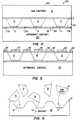
- Figs. 1-17provide an improved method of fabricating a microstructure onto a substrate.
- Figs. 1-17are, for example, in context to fabricating and assembling a shaped gallium arsenide block onto a silicon substrate for illustrative purposes only.
- trapezoidal shaped blocksself-align into inverted trapezoidal shaped recessed regions located on the top surface of the silicon wafer.
- Steps for such methodinclude forming the gallium arsenide blocks, transferring the blocks into a solution forming a slurry, and spreading the slurry evenly over the top surface of a silicon substrate having recessed regions. During the spreading steps, the blocks self-align and settle into the recessed regions while being transported with the fluid across the top surface.
- the details of fabricating the silicon substrate having recessed regionswill be discussed in detail below after a brief discussion of forming the gallium arsenide blocks.
- the methodprovides as an example a step of forming trapezoidal shaped blocks from a gallium arsenide wafer.
- Such stepincludes providing a gallium arsenide wafer 10 as illustrated in Fig. 1.
- the methodalso provides forming sacrificial layer 13 by chemical vapor deposition, sputtering, or the like overlying top surface 15 of gallium arsenide wafer 10.
- sacrificial layer 13includes, for example, aluminum arsenide.
- Other sacrificial layersmay include indium phosphate, silicon dioxide, photoresist, among other materials capable of being selectively etched. Of course, the sacrificial layer used depends upon the particular application.
- thickness for such layeris between about 0.1 ⁇ m and about 5.0 ⁇ m, and preferably at about 1 ⁇ m.
- a step of etching top surface 15 by methods such as wet etching, plasma etching, or reactive ion etchingclears off any native oxide.
- a step of desorption in the presence of arsenicremoves the native oxide layer.
- a subsequent step of preferential etchingremoves sacrificial layer 13 to facilitate the lift-off of each gallium arsenide block (also called a mesa shaped or trapezoidal shaped or truncated pyramid shaped structure) formed overlying sacrificial layer 13.
- gallium arsenide layer 17forms overlying sacrificial layer 13.
- Such gallium arsenide layermay be fabricated by methods including molecular beam epitaxy, chemical vapor deposition, and others.
- the thickness (T) of the gallium arsenide layeris at least about 10 nm and greater, and preferably at about 10 ⁇ m and greater, depending upon the particular application.
- the improved methodprovides the steps of masking and etching gallium arsenide layer 17.
- Fig. 2illustrates gallium arsenide substrate 10 after such masking and etching steps and includes gallium arsenide blocks 19 and a photoresist layer 21 overlying gallium arsenide layer 17 (not shown).
- unexposed portions of gallium arsenide layer 17are etched up to sacrificial layer 13 as illustrated in Fig. 2.
- Such etching stepprovides a plurality of shaped gallium arsenide blocks 19.
- the shaped blocksinclude a trapezoidal profile or truncated pyramid shape.
- Such trapezoidal profilemay be fabricated by methods of wet etching, plasma etching, ion milling, reactive ion etching, among others, depending on the application.
- a wet etchproduces a sloping profile along the sides or edges of each gallium arsenide block.
- a wet etchproduces an outward sloping profile as illustrated in Fig 2.
- mask edges parallel to the [110] directionproduces an inward sloping (or reverse mesa) profile.
- the outward sloping profileprovides a desired shape which integrates into a silicon substrate having recessed regions shaped in a complementary manner.
- Ion millingproduces gallium arsenide blocks with outward sloping profiles, depending upon the beam angle.
- Beam angleis adjusted between about 0° to about 30° from a normal to top surface 15 on gallium arsenide substrate 10.
- the entire structureis typically rotated during such etching step.
- Reactive ion etchingalso produces gallium arsenide blocks having a shaped profile.
- etching methodcreates blocks having undercut sides or a reverse mesa profile.
- etching methodmay create blocks having substantially consistent shapes and/or profiles.
- trapezoidal shaped blocksare removed through a lift-off technique from gallium arsenide substrate 10 by preferential etching sacrificial layer 13 as illustrated in Fig. 3.
- Such lift-off techniqueoccurs by, for example, a preferential wet etch of the aluminum arsenide sacrificial layer.
- wet etching stepis typically performed by a chemical such as a hydrofluoric acid solution or the like.
- the etchant usedsubstantially etches the sacrificial layer but does not aggressively attack gallium arsenide blocks and/or substrates.
- the wet etchant solutionAfter separating the gallium arsenide blocks from substrate 10, methods of diluting and decanting the wet etchant solution remove the blocks from the solution.
- the wet etchantis diluted and decanted using purified water, methanol, ethanol, or the like.
- a rinsing stepoccurs after the diluting and decanting step.
- the rinsing steprelies on solutions such as acetone, methanol, ethanol, or any other inert solution having low corrosive properties.
- Such solutionalso provides a medium (or fluid) for creating a mixture having blocks suspended therein or generally a slurry.
- an alternative lift-off methodcreates intermediate structure 250 of Fig. 4 from the gallium arsenide structure of Fig. 2.
- Such alternative lift-off methodalso promotes lift-off of the shaped blocks in applications where the devices are formed onto the backside of the blocks.
- the methodincludes spreading a filler or wax layer 253 preferably high temperature wax overlying the top surface of exposed portions of sacrificial layer 13 and gaps 255 between each block 19.
- One such waxincludes a product by the name of TECH WAX made by TRANSENE Co., Inc.
- the methodthen includes inverting the gallium arsenide structure of Fig. 2 and attaching top surface 21 onto intermediate substrate 257.
- Such intermediate substrateis, for example, a silicon wafer or the like.
- intermediate substrate surface 261undergoes steps of etching off any native oxide preferably with a wet etchant such as hydrofluoric acid, and treating the cleaned surface with an adhesion promotor such as hexamethyldisilazane also called HMDS.
- HMDShexamethyldisilazane
- backside 263is lapped about 50 ⁇ m remains on substrate 10. The remaining thickness of substrate 10 is then etched up to aluminum arsenide layer 13.
- An etchantsuch as ammonium hydroxide and hydrogen peroxide (6:200 NH 3 OH:H 2 O 2 ) preferentially etches the gallium arsenide substrate up to aluminum arsenide layer 13. Accordingly, the aluminum arsenide layer acts as an etch stop protecting gallium arsenide blocks 19. Removing aluminum arsenide layer 13 requires a step of wet etching using an etchant such as hydrofluoric acid. Such etchant typically removes aluminum arsenide layer 13 after a short dip in such solution. After the aluminum arsenide layer is completely removed, steps including masking, sputtering, and etching form metallized ring contacts 265 as illustrated in Fig. 5.
- Such metallized ring contactswere made by patterns formed from photoresist layer 267.
- the metallization for such contactsinclude materials such as gold, aluminum, among others.
- other processing stepssuch as etching, masking, implantation, diffusion, and the like may be performed on the blocks to create other profiles as well as active devices thereon.
- a solutionsuch as trichloroethane (TCA) dissolves the filler or wax disposed between each block 19 and photoresist layer 21, and lifts off the gallium arsenide blocks 19 from intermediate substrate 257.
- TCAtrichloroethane
- the gallium arsenide blocksare transferred to an inert solution such as acetone, methanol, ethanol, or any other solution having low corrosive characteristics.
- inert solution and blocksare often called a mixture or generally a slurry.
- the slurrycomprises an inert solution (of fluid) and shaped blocks. Enough solution exists in the slurry to allow the blocks to slide across the top surface of the substrate.
- the amount of solution in the mixtureis at least the same order as the amount of blocks. Of course, the amount of solution necessary depends upon characteristics such as block size, block material, substrate size, substrate material, and solution.
- the slurryis transferred or spread over top surface 53 of silicon substrate 50 as illustrated in Fig. 6. The details of the transferring technique are discussed below after a brief discussion in fabricating silicon substrate 50.
- silicon substrate 50comprises etched recessed regions 55.
- a variety of techniquesincluding wet etching, plasma etching, reactive ion etching, ion milling, among others provide recessed regions 50, or generally trenches, receptors, or binding sites. Such techniques etch recessed regions 50 with a geometric profile which is complementary to block 19.
- each recessed regionincludes a trapezoidal profile or inverted truncated pyramid shape. The trapezoidal profile allows block 19 to self-align and fit closely into recessed region 50 via the improved transferring technique.
- the transferring techniqueincludes a step of evenly spreading or pouring the slurry over top surface 53.
- the transferring techniquemay be accomplished by pouring a vessel of slurry evenly over top surface 53.
- the slurrymay also be transferred from a pipet, flask, beaker, or any other type of vessel and/or apparatus capable of evenly transferring the slurry over top surface 53.
- the slurryis poured over top surface 50 at a rate which allows substantial coverage of the top surface, but prevents blocks already disposed into the recessed regions from floating or popping out.
- Slurry flowis typically laminar but can be non-laminar, depending upon the particular application.
- the fluid flux over top surface 53occurs at a velocity between about 0.01 mm/sec. and about 100 mm/sec. Preferably, fluid flux occurs at about 1 mm/sec.
- the blocksflow evenly with the fluid, tumble onto top surface 53, self-align, and settle into recessed regions 55.
- the transferring stepmay take place in a centrifuge or the like. A centrifuge, for example, places a force on the blocks already disposed in the recessed regions and thereby prevents such blocks from floating out with solution.
- the resulting structure 20 of the method described by Figs. 1-3 and 6is illustrated in Fig. 7.
- the assembled microstructureincludes silicon substrate 10, gallium arsenide blocks 19, and recessed regions 55.
- the trapezoidal shape of the blocks and recessed regionsallows a block to self-align and fit closely into a recessed region during the transferring step.
- An angle (A) formed between one side of the block and the corresponding side of the recessed regionis between about substantially 0° to about 20°. Preferably, such angle is less than about 5° but greater than substantially 0°. Such angle facilitates the self-alignment process of each block.
- the improved methodallows for the fabrication of multiple blocks or microstructures onto a substrate by various shaped blocks and recessed region geometries and the fluid transferring step.
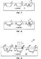
- the blocks 19are attached into recessed regions 55 through eutectic layer 75 as represented in structure 70 of Fig. 8.
- a metallized layersuch as gold, silver, solder, or the like is formed onto surface 73.
- the layer attaching the block with each recessed regionmay be a synthetic adhesive or the like instead of a eutectic layer. Process steps comprising masking, etching, and sputtering typically form such metallized layer.
- heating structure 70forms eutectic layer 75 between metallization layer 73 and silicon substrate 10.
- the eutectic layerprovides both mechanical and electrical contact between substrate 10 and block 19.
- the method of attaching the blocks onto the substrateprovides an efficient, cost effective, and easy technique.
- the portions of the improved method of Figs. 1, 2, 4, 5, and 6provides the resulting gallium arsenide light emitting diodes (LED) 200 as illustrated in Fig. 9.
- the gallium arsenide LEDincludes silicon substrate 203 and gallium arsenide block 205.
- Each gallium arsenide blockincludes at least metallized ring contacts 207, p-type gallium arsenide layer 209, n-type gallium arsenide layer 211, and eutectic layer 213.
- voltageis applied to metallized ring contact 207 or metallization layer. Photons (h ⁇ ) are illuminated from a center region within each metallized ring contact 207 of gallium arsenide block 205 as shown.
- the improved structureforms gallium arsenide light emitting diodes (LED) 90 as depicted in Fig. 10.
- the gallium arsenide LEDincludes silicon substrate 93 and gallium arsenide block 95.
- Each gallium arsenide blockalso includes at least metallized surface 97, p-type gallium arsenide layer 101, n-type gallium arsenide layer 103, and eutectic layer 105, similar to the preceding embodiment.
- voltageis applied to metallization layer 97 by, for example, a probe. Photons (h ⁇ ) are illuminated from an edge region instead of a center region of gallium arsenide block 95 as shown.
- the improved structureforms gallium arsenide structure 120 having tapered aperture opening 123 as illustrated in Fig. 11 (not to scale).
- a process stepsuch as wet etching, ion milling, reactive ion etching, and others forms the tapered aperture opening 123.
- the gallium arsenide structuremay be an LED, laser, or the like.
- gallium arsenide structure 120includes substrate 125 and gallium arsenide block 127.
- Structure 120also includes a top metallization layer 131 such as aluminum overlying gallium arsenide block 127 and an insulating layer 133.
- a ring contact layer 135provides mechanical and electrical contact between substrate 125 and gallium arsenide block 127.
- a light emitting (or lasing) aperture 139having a dimension between about 5 ⁇ m and about 40 ⁇ m.
- voltageis applied to metallization layer 131.
- Photons (h ⁇ )illuminate from gallium arsenide block 127, through light emitting aperture 139, and through tapered aperture opening 123 as shown.
- Fiber optic cable 141receives the photons.
- Such fiber optic cableincludes a tapered receiver end with a diameter between about 50 ⁇ m and about 200 ⁇ m.
- the improved method and resulting structureare in context to a trapezoidal shaped block made of gallium arsenide merely for illustrative purposes only.
- the improved method and structurecan be in context to almost any block having shaped features.
- Shaped featuresallow such blocks to move over the surface of the substrate via fluid transport, align with a corresponding recessed region, and insert into such recessed region.
- Fig. 12illustrates further examples of the shaped blocks.
- the blocksmay, for example, include a rectangular shape 300, octagonal shape 303, or circular shape 305.
- the rectangular shaped blockincludes up to four orientations for insertion into a substrate having a corresponding recessed region.
- the octagonal shaped blockincludes up to eight orientations and the circular shaped block includes continuous orientations as long as the narrow end inserts first into the recessed region.
- Such blocksmay also comprise a material such as silicon, gallium arsenide, aluminum gallium arsenide, diamond, germanium, other group III-V and II-VI compounds, multilayered structures, among others.
- Such multilayered structuresmay include metals, insulators such as silicon dioxide, silicon nitride and the like, and combinations thereof.
- the blockcan be made of almost any type of material capable of forming shaped features.
- such blocksare fabricated by methods including ion milling, reactive ion etching, and the like.
- an angle between a side of the block and the corresponding side of the recessed region for a disposed blockis between about substantially 0° to about 20°. Preferably, such angle is less than about 5° but greater than substantially 0°.
- the shaped blockassembles with a substrate such as a silicon wafer, plastic sheet, gallium arsenide wafer, glass substrate, ceramic substrate, or the like.
- the substrateincludes almost any type of material capable of forming shaped recessed regions or generally binding sites or receptors thereon which complement the shaped blocks.
- a gallium arsenide block in the form of a diodewas assembled onto a silicon substrate and operated.
- a slurry including gallium arsenide blockswere transferred such that the blocks self-aligned into recessed regions located on a top surface of a silicon substrate.
- the steps for such methodincluded forming the gallium arsenide blocks, transferring the blocks into a solution forming a slurry, and transporting the slurry evenly over a top surface of a silicon substrate having recessed regions.
- the shaped blocksgenerally tumble onto the top surface of the substrate, self-align and engage with a recessed region having a complementary shape.
- a solution of ethylenediamine pyrocatechol pyrazine (EDP) or potassium hydroxide (KOH)produced recessed regions having a trapezoidal profile or inverted truncated pyramid shape.
- EDPethylenediamine pyrocatechol pyrazine
- KOHpotassium hydroxide
- Trapezoidal profilesoccurred due to the selectivity (1:100) between the ⁇ 111 ⁇ plane and the ⁇ 100 ⁇ or ⁇ 110 ⁇ plane.
- the ⁇ 111 ⁇ planeetched slower than the ⁇ 100 ⁇ or ⁇ 110 ⁇ plane by a ratio of 1:100.
- an EDP solutionetched recessed regions into a silicon substrate.
- EDPincludes ethylenediamine (about 500 ml.), pyrocatechol (about 160 gms.), water (about 160 gms.), pyrazine (about 1 gm.).
- the EDP bathwas also at a temperature of about 115 °C.
- a thermal oxide (SiO 2 ) layerhaving a thickness of about 200 nm was first formed on a top surface of such substrate. Masking and etching such oxide layer formed rectangular shaped regions. Such regions were then etched vertically about 10 ⁇ m forming square openings on the top surface about 23 ⁇ m in length. Sides protrude down symmetrically from each opening to a square base having a length of about 9 ⁇ m.
- an epi-ready two inch (5 cm) n-type gallium arsenide waferprovided a substrate for the formation of the self-aligning blocks.
- Native oxide on the top surface of such blockwas first cleared off by a desorption process.
- the desorption processincluded exposing the wafer to a temperature of about 700 °C and elements including arsenic.
- a sacrificial layercomprising 1 ⁇ m of doped or undoped aluminum arsenide was grown on and in contact with the top surface.
- a thickness of about 10.7 ⁇ m of silicon doped gallium arsenidewas then grown through an MBE process overlying the aluminum arsenide layer. Silicon dopants were at a concentration of about 10 18 atoms/cm 3 .
- the top surface of the MBE grown layerwas then patterned with photoresist.
- Patterning the top surface of the MBE grown layerincluded spreading a photoresist layer having a thickness of about 1.6 ⁇ m over the top surface of the MBE grown gallium arsenide layer.
- the photoresist usedis a product made by Shipley under the name of AZ1400-31.
- Patterning stepsalso included at least exposing, developing, and baking the photoresist. Such baking step occurred at a temperature of about 120 °C for about 1 hour to hard-bake the photoresist layer.
- the patterning stepsformed a plurality of rectangles each having a dimension of about 35 ⁇ m by 24 ⁇ m (exposed portions of the photoresist) on the top surface.
- wet etching the unexposed regionsproduced results which depended upon the orientation of the mask edges. If the mask edges were parallel to the [1 1 0] direction, wet etching the unexposed regions created outward sloping profiles from the top surface of each block. Alternatively, wet etching unexposed regions where mask edges were parallel to the [110] direction created inward sloping (or reverse mesa) profiles.
- gallium arsenideincludes two distinct sets of ⁇ 111 ⁇ planes.
- each gallium atom on the surfacehas three arsenide atoms bonded below.
- each arsenide atom on the surfaceincludes three gallium atoms bonded below.
- Each arsenide atom in the ⁇ 111 ⁇ B layerincludes a pair of dangling electrons and is therefore exposed. Such dangling electrons are not present in the structure of the ⁇ 111 ⁇ A plane. Accordingly, ⁇ 111 ⁇ B planes tend to etch faster than ⁇ 111 ⁇ A planes, thereby forming blocks having a reverse mesa shape which is generally incompatible with the recessed regions etched on the silicon substrate.
- Mask edges parallel to the [110] planeproduced more undercutting than the cases where mask edges were parallel to the [1 1 0] plane.
- mask edges parallel to the [110] directionproduced about 1.1 ⁇ m of horizontal etching per micron of vertical etching near the tops of the blocks. Regions near the base of the blocks produced etches of about 0.4 ⁇ m of horizontal etching per micron of vertical etching.
- mask edges parallel to the [1 1 0] planeproduced etches of about 0.8 ⁇ m of horizontal etching per micron of vertical etching for regions near the top of the blocks, and 0.1 ⁇ m of horizontal etching per micron of vertical etch near the bottom of the blocks.
- the formation of a square region at the baserequired a longer mask in the [110] direction.
- etchant concentrationalso affected the shape of each gallium arsenide block.
- a solution of phosphoric acid, hydrogen peroxide, and water(H 2 PO 3 :H 2 O 2 :H 2 O) provided a promising etchant for the MBE grown gallium arsenide layer in the present example.
- Such etchantcreated three distinct profiles, depending upon the amount of hydrogen peroxide and water added to phosphoric acid.
- Dilute concentrations of phosphoric acid(1:1:40 H 2 PO 3 :H 2 O 2 :H 2 O) created a trapezoidal or mesa shaped profile having a 30° angle between the top surface of the block and a corresponding side.
- Etchant solutionswhich were less concentrated produced shallower trapezoidal or mesa shaped profiles at angles from ' about 10° to 20°. Such shallower profiles were probably a result of etching reactions being transport limited in the ⁇ 111 ⁇ B planes.
- phosphoric acid(1:1:20 H 2 PO 3 :H 2 O 2 :H 2 O and above) created inward sloping (or reverse mesa) profiles limited by the reaction of the ⁇ 111 ⁇ B planes.
- a phosphoric acid concentration(1:1:30 H 2 PO 4 :H 2 O 2 :H 2 O) between the dilute and concentrated solutions provides better profiles for assembly with recessed regions etched on the silicon substrate.
- Such etchantproduced blocks having angles of 55° parallel to the [110] plane and 49° parallel to the [1 1 0] plane, and typically etched the MBE grown layer at a rate of about 0.133 ⁇ m/minute (or about 133 nm/min). In producing the results described, etchant solution was typically replenished when depleted.
- a similar wet etchant(1:1:30 H 2 PO 3 :H 2 O 2 :H 2 O) facilitated the formation of aluminum gallium arsenide blocks from an aluminum gallium arsenide MBE grown layer.
- the presence of aluminum arsenideincreased etching of the ⁇ 111 ⁇ B plane into the reaction-rate limited regime.
- ion millingwas also used to create the gallium arsenide trapezoidal shaped blocks.
- Ion milling the MBE grown gallium arsenide layerprovided outward sloping profiles ranging at angles of about 68° to 90° between the top surface and a corresponding side. To produce such angles, the ion beam angles ranged from about 0° to 25° in reference to a normal from the top surface of the MBE grown layer. Steeper beam angles (closer to 90°) generally created vertical or substantially vertical profiles. Ion milling also required the substrate to be rotated about a center axis during such processing step.
- processing variablesincluded an argon gas etchant, pressure of about 50 millitorr, ion energy of about 1000 v, and an ion milling rate of 1 ⁇ m every seven minutes.
- argon gas etchantpressure of about 50 millitorr
- ion energyof about 1000 v
- ion milling rate1 ⁇ m every seven minutes.
- the photoresist maskeroded laterally about 5 ⁇ m every 70 minutes during milling, sidewalls having angles at about 68° were produced.
- Selectivity between the gallium arsenide and photoresistwas about 3:1. Ion milling produced substantially consistent gallium arsenide blocks and was therefore more effective than wet etching in this particular example.
- a final bath having a concentration of 1:1:30 H 2 PO 3 :H 2 O 2 :H 2 Owas used to clear off remaining oxides of either gallium arsenide and aluminum arsenide. Such oxides were typically formed when aluminum arsenide was exposed to etching baths or ion milling. Hydrofluoric acid may then be used to clear off the oxide layers (typically rough looking and brown in appearance). Generally, such oxide layers reduce the effectiveness of hydrofluoric acid (HF) etching on the sacrificial aluminum arsenide layer.
- HFhydrofluoric acid
- a HF solutionpreferentially etched the sacrificial layer of aluminum arsenide to lift-off the gallium arsenide blocks.
- a HF solution having a concentration of about 5:1 H 2 O:HFwas used to etch the sacrificial layer and lift off the blocks. Any blocks still remaining on the substrate possibly through surface tension can be mechanically removed from the substrate into a solution. Removed blocks include a base dimension of about 22 ⁇ m by 23 ⁇ m, compared to a designed dimension of 24 ⁇ m by 24 ⁇ m.
- a teflon pipetwas used to remove a substantial portion of the HF solution from the gallium arsenide blocks. Any remaining HF was rinsed off with water. Such rinsing step created a mixture including blocks and water. An inert solution such as acetone then replaced the water to decrease any oxide formation on the blocks. Once in the inert solution, the blocks may cluster together and either float to the surface or settle to the bottom of the solution. Such clusters, often visible to the naked eye, decreased the effectiveness of a subsequent transferring step, and were therefore separated by mechanically agitating the solution with ultrasonic vibration.
- the inert solution including gallium arsenide blockswere then transferred (or poured) evenly over the top surface of the silicon substrate.
- a pipetwas used to transfer such solution over the top surface of the substrate.
- the solutionis transferred at a rate creating substantially a laminar flow.
- Such laminar flowallowed the blocks to tumble and/or slide onto the top surface of the substrate and then self-align into the recessed regions via the trapezoidal profile.
- the transfer rateshould provide an even flow of solution including blocks over the substrate surface but should not free or remove any blocks already disposed into the recessed regions.
- Blocks fabricated by ion millingproduced higher yields than wet etched blocks.
- Ion milled blocks having substantially consistent profilesself aligned and inserted into more than 90% of the recessed regions located on the substrate surface before the solution substantially evaporated. As the solution evaporates, , surface tension often pulled a portion of the blocks out of the recessed regions. About 30% to 70% of the recessed regions remained filled after evaporation. The decrease in yield can be addressed by using liquids having lower surface tension during evaporation or by super critical drying methods which substantially eliminates surface tension.
- blocksmay be bonded into the recessed regions prior to evaporation of the solution, thereby fixing the yield.
- Photographs shown in Fig. 13illustrate gallium arsenide blocks disposed into recessed regions of the silicon substrate 150 according to the present example.
- a top portion 153 of each recessed regionis square and measures about 23 ⁇ m at length.
- the photographincludes recessed regions 155, silicon substrate 157, and trapezoidal shaped block 159.
- an illuminated diode 170is shown in the photograph of Fig. 14.
- the photographincludes silicon substrate 173 and illuminated gallium arsenide LED 175.
- the gallium arsenide LEDemitted infrared radiation while under electrical bias.
- Each gallium arsenide LED which was grown on an MBE layerincluded an N+ gallium arsenide cap layer (about 100 nm thickness), an N+ Al 0.1 Ga 0.9 As transport layer (about 1 ⁇ m thickness), a P- active region (about 1 ⁇ m thickness), and a P+ buffer layer (about 1 ⁇ m thickness).
- the gallium arsenide LEDalso required a ring metallized contact 400 for applying voltage and an opening 403 for light output at a top portion of each block as illustrated in Fig. 15.
- a current-voltage (I-V) curve 500 illustrated in Fig. 16exhibits typical p-n junction characteristics for the gallium arsenide structure of Fig. 14.
- RTD'sGallium arsenide/aluminum arsenide resonant-tunneling diodes
- RTD's grown on an MBE layerinclude gallium arsenide wells (depth at about 5.0 nm) between two aluminum arsenide barriers (depth at about 2.5 nm).
- Oscillations (rf) observed after biasing the RTD's in the NDR regionwere limited to about 100 MHz. External capacitances and inductances of the biasing circuit caused such limitations in frequency.
- the description aboveis in terms of assembling a gallium arsenide block onto a silicon substrate for illustrative purposes only. As shown, the invention may be applied to forming gallium arsenide diodes onto silicon substrates.
- Another commercial applicationincludes gallium arsenide lasers assembled with silicon integrated circuits. The silicon chips can communicate with other chips with integrated optical detectors on extremely high bit-rate optical channels. Other applications may also include integration of microwave gallium arsenide devices onto silicon integrated circuits for the purpose of microwave electronics.
- Still a further applicationincludes microstructures integral with a plastic sheet forming active liquid crystal displays (ALCD) and the like. In such application, the plastic sheet may be fabricated by a technique including stamping, injection molding, among others.
- the concept of the inventioncan be used with almost any type of microstructure which assembles onto a larger substrate.
- the block structuremay also include a variety of shapes such as a cylindrical shape, rectangular shape, square shape, hexagonal shape, pyramid shape, T-shape, kidney shape, and others.
- the block structureincludes widths, lengths, and heights to promote self-assembly for a desired orientation.
- more than one type of structuremay be present in the mixture (solution and blocks) as long as each structure includes a specific binding site on the substrate.
Landscapes
- Engineering & Computer Science (AREA)
- Microelectronics & Electronic Packaging (AREA)
- Power Engineering (AREA)
- Computer Hardware Design (AREA)
- Physics & Mathematics (AREA)
- General Physics & Mathematics (AREA)
- Condensed Matter Physics & Semiconductors (AREA)
- Manufacturing & Machinery (AREA)
- Nonlinear Science (AREA)
- Crystallography & Structural Chemistry (AREA)
- Chemical & Material Sciences (AREA)
- Mathematical Physics (AREA)
- Optics & Photonics (AREA)
- Led Devices (AREA)
- Weting (AREA)
- Die Bonding (AREA)
- Drying Of Semiconductors (AREA)
- Semiconductor Lasers (AREA)
- Optical Elements Other Than Lenses (AREA)
- Led Device Packages (AREA)
- Diaphragms For Electromechanical Transducers (AREA)
- Polishing Bodies And Polishing Tools (AREA)
Abstract
Description
- The present invention relates to the field of electronicintegrated circuits. The invention is illustrated in an example withregard to the manufacture of gallium arsenide microstructures onto asilicon substrate, but it will be recognized that the invention willhave a wider range of applicability. Merely by way of example, theinvention may be applied in the manufacture of devices containingsilicon based electronic devices integrated with a gallium arsenidebased microstructures (or devices) such as light emitting diodes(LED), lasers, tunneling transistors, Gunn oscillators, integratedcircuits, solar collectors, and others.
- Industry currently needs a cost effective, efficient, andpractical method for assembling a higher cost microstructure onto alower cost commercially available substrate. In particular, amaterial such as gallium arsenide possesses substantially bettercharacteristics for some specific electronic and opto-electronicapplications rather than materials such as silicon. However, in thefabrication of gallium arsenide devices, substantial regions of agallium arsenide wafer are typically unused and wasted. Such unusedregions generally create an inefficient use of precious die area. Inaddition, processing gallium arsenide typically requires specialtechniques, chemicals, and equipment, and is therefore costly.
- Other applications such as very large scale integrated(VLSI) circuits may be better fabricated in silicon rather thangallium arsenide. In still further applications, it may be desirableto produce integrated circuits having characteristics of both typesof materials. Accordingly, industry needs to develop an effectivemethod of fabricating a gallium arsenide device integrated with asilicon based integrated circuit. The resulting structure of suchmethod includes advantages of both gallium arsenide and silicon baseddevices.
- Methods such as flip chip bonding, lift off methods, andothers, generally require large areas of a substrate and areincompatible with a micron sized state-of-art microstructure. Suchmethods often create difficulty in positioning a particle onto asubstrate. Accordingly, industry needs to develop an effective method of fabricating higher cost materials such as a galliumarsenide microstructure onto a lower cost substrate such as silicon.
- Industry utilizes or has proposed several methods forfabricating individual electronic components (or generallymicrostructures) and assembling such structures onto a substrate.One approach is to grow gallium arsenide devices directly onto asilicon substrate. This approach becomes limiting because thelattice structure of gallium arsenide mismatches that of silicon. Inaddition, growing gallium arsenide onto silicon is inherently10 difficult and therefore costly. Accordingly, gallium arsenide cannot efficiently be grown on a silicon substrate.
- Another approach is described by Sliwa in U.S. Patent No.4,990,462, in which a method for coplanar integration ofsemiconductor IC devices bringing together segments in perfectthree-dimensional alignment and in perfect particulate-freefashion with a high throughput and exacting reproducibility atlow cost is achieved by the use of a liquid surface-tensiondriven flotation and assembly mechanism. In essence, thesegments pull themselves together to minimize surface tensionand in doing so, the liquid self-limits and hydrodynamicallydamps the maximum forces to which the segments are exposed.
- Another approach disclosed in U.S. Patent No. 4,949,148 byBartelink deals with a self-aligning integrated circuitassembly. Therein, the microstructure integral with asubstrate comprising a substrate or carrier wafer having aplurality of recess regions or apertures thereon and aplurality of shaped blocks or pin blocks integral with saidrecess regions is comprised, wherein shaped blocks include anintegrated circuit or IC die thereon.
- Another approach is described by Yando in U.S. Patent No.3,439,416. Yando describes components or structures placed, trapped,or vibrated on an array of magnets. Such magnets include magnetizedlayers alternating with non-magnetized layers to form a laminatedstructure. Components are matched onto the array of magnets formingan assembly thereof. However, severe limitations exist on the shape,size, and distribution of the components. component width must matchthe spacing of the magnetic layers and the distribution of componentsare constrained by the parallel geometry of lamination. In addition,self-alignment of components requires the presence of the laminatedstructure. Furthermore, the structures disclosed by Yando typicallypossess millimeter sized dimensions and are therefore generallyincompatible with micron sized integrated circuit structures.Accordingly, the method and structure disclosed by Yando is therebytoo large and complicated to be effective for assembling a state-of-artmicrostructure or component onto a substrate.
- Another approach involves mating physical featuresbetween a packaged surface mount device and substrate as described inU.S. Patent No. 5,034,802, Liebes, Jr. et al. The assembly processdescribed requires a human or robotics arm to physically pick, align,and attach a centimeter sized packaged surface mount device onto asubstrate. Such process is limiting because of the need for thehuman or robotics arm. The human or robotics arm assembles eachpackaged device onto the substrate one-by-one and not simultaneously,thereby limiting the efficiency and effectiveness of the operation.Moreover, the method uses centimeter sized devices (or packed surfacemount integrated circuits), and would have little applicability withmicron sized integrated circuits in die form.
- Another approach, such as the one described in U.S.Patent No. 4,542,397, Biegelsen et al. involves a method of placingparallelogram shaped structures onto a substrate by mechanicalvibration. Alternatively, the method may also employ pulsating airthrough apertures in the support surface (or substrate). Alimitation to the method includes an apparatus capable of vibrating the structures, or an apparatus for pulsating air through theapertures. Moreover, the method described relies upon centimeter-sizeddies and would have little applicability with state-of-artmicron sized structures.
- A further approach such as that described in U.S. PatentNo. 4,194,668 by Akyurek discloses an apparatus for aligning andsoldering electrode pedestals onto solderable ohmic anode contacts.The anode contacts are portions of individual semiconductor chipslocated on a wafer. Assembling the structures requires techniques ofsprinkling pedestals onto a mask and then electromagnetic shakingsuch pedestals for alignment. The method becomes limiting because ofthe need for a shaking apparatus for the electromagnetic shakingstep. In addition, the method also requires a feed surface gentlysloping to the mask for transferring electronic pedestals onto themask. Moreover, the method is solely in context to electrodepedestals and silicon wafers, thereby limiting the use of such methodto these structures.
- Still another approach requires assembling integratedcircuits onto a substrate through electrostatic forces as describedin Application Serial No. 07/902,986 filed June 23, 1992 by Cohn, published on 18 October 1994 as US 5 355 577.The electrostatic forces vibrate particles such that the particlesare arranged at a state of minimum potential energy. A limitationwith such method includes providing an apparatus capable of vibratingparticles with electrostatic forces. Moreover, the method of Cohncreates damage to a portion of the integrated circuits bymechanically vibrating them against each other and is also generallyineffective. Accordingly the method typically becomes incompatiblewith a state-of-art microstructure.
- From the above it is seen that a method of assembling amicrostructure onto a substrate that is compact, low cost, efficient,reliable, and requires little maintenance is desired.
- The present invention pertains to a method and resultingstructure for assembling a microstructure onto a substrate. Inparticular, the method includes transferring shaped blocks orgenerally structures via a fluid onto a top surface of a substratehaving recessed regions or generally binding sites or receptors.Upon transferring, the blocks self-align through their shape into therecessed regions, and integrate thereon. The resulting structure mayinclude a variety of useful electronic integrated circuits containingsilicon based electronic devices integrated with a gallium arsenidebased microstructures such as a light emitting diodes (LED), lasers,tunneling transistors, Gunn oscillators, integrated circuits, solarcollectors, and others.
- In one specific embodiment, the method providesassembling a microstructure such as a micron sized block onto asubstrate. The substrate includes a top surface with at least onerecessed region thereon and may be either a silicon wafer, galliumarsenide wafer, glass substrate, ceramic substrate, or others. Thesubstrate may also be a plastic sheet fabricated from a techniquesuch as stamping, injection molding, among others. Assembling stepsinclude providing shaped blocks, and transferring the blocks into afluid to form a mixture thereof or generally a slurry. Such slurryis then dispensed evenly over the substrate at a rate where at leastone of the shaped blocks is disposed into a recessed region.Dispensing occurs at substantially a laminar flow and allows aportion of the shaped blocks to self-align into the recessed region.
- The method providesshaped blocks having a trapezoidal profile from an improvedfabrication process. Fabrication includes providing a secondsubstrate having a top surface, and growing a sacrificial layeroverlying the top surface. A step of forming a block layer overlyingthe top surface is then performed. Masking and etching the blocklayer up to the sacrificial layer creates trapezoidal shaped blocksthereon. A step of preferential etching the sacrificial layer liftsoff each trapezoidal shaped block. Such blocks are then rinsed andtransferred into a solution forming the slurry.
- The shaped block comprises atruncated pyramid shaped gallium arsenide structure. The truncatedpyramid shaped structure includes a base with four sides protrudingtherefrom to a top surface. Each side creates an angle between about50° and about 70° from the base to a side. Each side may also have aheight between about 5 µm and about 15 µm. The base may have alength between about 10 µm and about 50 µm, and a width between 10 µmand about 50 µm.
- The improved method is incontext to a trapezoidal shaped block made of gallium arsenideassembled onto a silicon substrate merely for illustrative purposesonly. The shaped blocks may also include a cylindrical shape,pyramid shape, rectangular shape, square shape, T-shape, kidneyshape, or the like (symmetrical and asymmetrical), and combinationsthereof. Generally, the shape of the block allows the block toclosely insert into a similarly shaped recessed region or receptor on a substrate. The shaped blocks also comprise a material such asgallium aluminum arsenide, silicon, diamond, germanium, other groupIII-V and II-VI compounds, multilayered structures, among others.Such multilayered structure may include metals, insulators such assilicon dioxide, silicon nitride, and the like, and combinationsthereof.
- A further understanding of the nature and advantages ofthe invention will become apparent by reference to the remainingportions of the specification and drawings.
- Fig. 1 is a gallium arsenide wafer having a molecularbeam epitaxy (MBE) grown gallium arsenide layer for the improvedmethod of fabrication;
- Fig. 2 is an illustration of trapezoidal shaped galliumarsenide blocks etched from an MBE grown gallium arsenide layer;
- Fig. 3 is an illustration for a lift-off step of galliumarsenide blocks;
- Fig. 4 is an illustration of a portion of an alternativelift-off step using a intermediate substrate;
- Fig. 5 is an illustration of another portion of thealternative lift-off step of Fig. 4;
- Fig. 6 is an illustration of each gallium arsenide blockself-aligning onto a silicon substrate;
- Fig. 7 is an embodiment of a microstructure assembledonto the silicon substrate according to the improved method depictedby Figs. 1-3 and 6;
- Fig. 8 is an alternative embodiment of a microstructureassembled onto a substrate;
- Fig. 9 is an embodiment of a microstructure assembledonto a substrate forming a gallium arsenide diode;
- Fig. 10 is an alternative embodiment of a microstructureassembled onto a substrate forming a gallium arsenide diode;
- Fig. 11 is a further alternative embodiment of amicrostructure assembled onto a substrate forming a gallium arsenidediode;
- Fig. 12 is an illustration of examples of shaped blocks;
- Fig. 13 is a photograph of an assembled microstructureaccording to the experiment; and
- Fig. 14 is a photograph of an operational photo diodeaccording to the experiment.
- Fig. 15 is a photograph of a metallized ring layeroverlying a gallium arsenide block;
- Fig. 16 is a current-voltage representation for a galliumarsenide diode according to the experiment; and
- Fig. 17 is a current-voltage representation for a galliumarsenide/aluminum arsenide resonant-tunneling diode according to theexperiment.
- With reference to Figs. 1-17, the present inventionprovides an improved method of fabricating a microstructure onto asubstrate. Figs. 1-17 are, forexample, in context to fabricating and assembling a shaped galliumarsenide block onto a silicon substrate for illustrative purposesonly.
- In the assembly of a gallium arsenide block onto asilicon wafer, trapezoidal shaped blocks self-align into invertedtrapezoidal shaped recessed regions located on the top surface of thesilicon wafer. Steps for such method include forming the galliumarsenide blocks, transferring the blocks into a solution forming aslurry, and spreading the slurry evenly over the top surface of asilicon substrate having recessed regions. During the spreadingsteps, the blocks self-align and settle into the recessed regionswhile being transported with the fluid across the top surface. Thedetails of fabricating the silicon substrate having recessed regionswill be discussed in detail below after a brief discussion of formingthe gallium arsenide blocks.
- In a specific embodiment, the method provides as anexample a step of forming trapezoidal shaped blocks from a galliumarsenide wafer. Such step includes providing a
gallium arsenidewafer 10 as illustrated in Fig. 1. The method also provides formingsacrificial layer 13 by chemical vapor deposition, sputtering, or thelike overlyingtop surface 15 ofgallium arsenide wafer 10. Suchsacrificial layer 13 includes, for example, aluminum arsenide. Othersacrificial layers may include indium phosphate, silicon dioxide,photoresist, among other materials capable of being selectivelyetched. Of course, the sacrificial layer used depends upon theparticular application. For an aluminum arsenide sacrificial layer,thickness for such layer is between about 0.1 µm and about 5.0 µm,and preferably at about 1 µm. Before formingsacrificial layer 13, astep of etchingtop surface 15 by methods such as wet etching, plasmaetching, or reactive ion etching clears off any native oxide.Alternatively, a step of desorption in the presence of arsenicremoves the native oxide layer. A subsequent step of preferentialetching (to be discussed in detail later) removessacrificial layer 13 to facilitate the lift-off of each gallium arsenide block (alsocalled a mesa shaped or trapezoidal shaped or truncated pyramidshaped structure) formed overlyingsacrificial layer 13. - In Fig. 1, gallium arsenide layer 17 forms overlying
sacrificial layer 13. Such gallium arsenide layer may be fabricatedby methods including molecular beam epitaxy, chemical vapordeposition, and others. The thickness (T) of the gallium arsenidelayer is at least about 10 nm and greater, and preferably at about 10µm and greater, depending upon the particular application. - To produce the desired dimensions for the block, theimproved method provides the steps of masking and etching galliumarsenide layer 17. Fig. 2 illustrates
gallium arsenide substrate 10after such masking and etching steps and includes gallium arsenideblocks 19 and aphotoresist layer 21 overlying gallium arsenide layer17 (not shown). Generally, unexposed portions of gallium arsenidelayer 17 are etched up tosacrificial layer 13 as illustrated in Fig.2. Such etching step provides a plurality of shaped gallium arsenideblocks 19. For the present example, the shaped blocks include atrapezoidal profile or truncated pyramid shape. Such trapezoidalprofile may be fabricated by methods of wet etching, plasma etching,ion milling, reactive ion etching, among others, depending on theapplication. - Generally, a wet etch produces a sloping profile alongthe sides or edges of each gallium arsenide block. For mask edgesparallel to the [1
1 0] direction, a wet etch produces an outwardsloping profile as illustrated in Fig 2. Alternatively, mask edgesparallel to the [110] direction, produces an inward sloping (orreverse mesa) profile. The outward sloping profile provides adesired shape which integrates into a silicon substrate havingrecessed regions shaped in a complementary manner. - Ion milling produces gallium arsenide blocks with outwardsloping profiles, depending upon the beam angle. Beam angle isadjusted between about 0° to about 30° from a normal to
top surface 15 ongallium arsenide substrate 10. To create the outward sloping(or truncated pyramid shape) profile for each block, the entirestructure is typically rotated during such etching step. - Reactive ion etching (RIE) also produces gallium arsenideblocks having a shaped profile. Generally, such etching methodcreates blocks having undercut sides or a reverse mesa profile.Depending upon variables such as the etchant, pressure, equipment,and others, such etching method may create blocks havingsubstantially consistent shapes and/or profiles.
- After etching the MBE grown layer, trapezoidal shapedblocks are removed through a lift-off technique from
gallium arsenidesubstrate 10 by preferential etchingsacrificial layer 13 asillustrated in Fig. 3. Such lift-off technique occurs by, forexample, a preferential wet etch of the aluminum arsenide sacrificiallayer. In the gallium arsenide example, such wet etching step is typically performed by a chemical such as a hydrofluoric acidsolution or the like. The etchant used substantially etches thesacrificial layer but does not aggressively attack gallium arsenideblocks and/or substrates. - After separating the gallium arsenide blocks from
substrate 10, methods of diluting and decanting the wet etchantsolution remove the blocks from the solution. In the galliumarsenide example, the wet etchant is diluted and decanted usingpurified water, methanol, ethanol, or the like. Optionally, arinsing step occurs after the diluting and decanting step. Therinsing step relies on solutions such as acetone, methanol, ethanol,or any other inert solution having low corrosive properties. Suchsolution also provides a medium (or fluid) for creating a mixturehaving blocks suspended therein or generally a slurry. - Instead of the lift-off technique illustrated in Fig. 3,an alternative lift-off method creates
intermediate structure 250 ofFig. 4 from the gallium arsenide structure of Fig. 2. Suchalternative lift-off method also promotes lift-off of the shapedblocks in applications where the devices are formed onto the backsideof the blocks. As shown, the method includes spreading a filler orwax layer 253 preferably high temperature wax overlying the topsurface of exposed portions ofsacrificial layer 13 andgaps 255between eachblock 19. One such wax includes a product by the nameof TECH WAX made by TRANSENE Co., Inc. The method then includesinverting the gallium arsenide structure of Fig. 2 and attachingtopsurface 21 ontointermediate substrate 257. Such intermediatesubstrate is, for example, a silicon wafer or the like. However,prior to the attaching step,intermediate substrate surface 261undergoes steps of etching off any native oxide preferably with a wetetchant such as hydrofluoric acid, and treating the cleaned surfacewith an adhesion promotor such as hexamethyldisilazane also calledHMDS. In removinggallium arsenide substrate 10,backside 263 islapped about 50 µm remains onsubstrate 10. The remaining thicknessofsubstrate 10 is then etched up toaluminum arsenide layer 13. Anetchant such as ammonium hydroxide and hydrogen peroxide (6:200NH3OH:H2O2) preferentially etches the gallium arsenide substrate uptoaluminum arsenide layer 13. Accordingly, the aluminum arsenidelayer acts as an etch stop protecting gallium arsenide blocks 19.Removingaluminum arsenide layer 13 requires a step of wet etchingusing an etchant such as hydrofluoric acid. Such etchant typicallyremovesaluminum arsenide layer 13 after a short dip in suchsolution. After the aluminum arsenide layer is completely removed,steps including masking, sputtering, and etching form metallized ringcontacts 265 as illustrated in Fig. 5. Such metallized ring contactswere made by patterns formed fromphotoresist layer 267. The metallization for such contacts include materials such as gold,aluminum, among others. Alternatively, other processing steps suchas etching, masking, implantation, diffusion, and the like may beperformed on the blocks to create other profiles as well as activedevices thereon. A solution such as trichloroethane (TCA) dissolvesthe filler or wax disposed between eachblock 19 andphotoresistlayer 21, and lifts off the gallium arsenide blocks 19 fromintermediate substrate 257. To decrease corrosion, the galliumarsenide blocks are transferred to an inert solution such as acetone,methanol, ethanol, or any other solution having low corrosivecharacteristics. Such inert solution and blocks are often called amixture or generally a slurry. - The slurry comprises an inert solution (of fluid) andshaped blocks. Enough solution exists in the slurry to allow theblocks to slide across the top surface of the substrate. Preferably,the amount of solution in the mixture is at least the same order asthe amount of blocks. Of course, the amount of solution necessarydepends upon characteristics such as block size, block material,substrate size, substrate material, and solution. After preparation,the slurry is transferred or spread over
top surface 53 ofsiliconsubstrate 50 as illustrated in Fig. 6. The details of thetransferring technique are discussed below after a brief discussionin fabricatingsilicon substrate 50. - As shown in Fig. 6,
silicon substrate 50 comprises etchedrecessedregions 55. A variety of techniques including wet etching,plasma etching, reactive ion etching, ion milling, among othersprovide recessedregions 50, or generally trenches, receptors, orbinding sites. Such techniques etch recessedregions 50 with ageometric profile which is complementary to block 19. In the siliconsubstrate, for example, each recessed region includes a trapezoidalprofile or inverted truncated pyramid shape. The trapezoidal profileallowsblock 19 to self-align and fit closely into recessedregion 50via the improved transferring technique. - The transferring technique includes a step of evenlyspreading or pouring the slurry over
top surface 53. Thetransferring technique may be accomplished by pouring a vessel ofslurry evenly overtop surface 53. Alternatively, the slurry mayalso be transferred from a pipet, flask, beaker, or any other type ofvessel and/or apparatus capable of evenly transferring the slurryovertop surface 53. Generally, the slurry is poured overtopsurface 50 at a rate which allows substantial coverage of the topsurface, but prevents blocks already disposed into the recessedregions from floating or popping out. Slurry flow is typicallylaminar but can be non-laminar, depending upon the particularapplication. In the gallium arsenide block example, the fluid flux overtop surface 53 occurs at a velocity between about 0.01 mm/sec.and about 100 mm/sec. Preferably, fluid flux occurs at about 1mm/sec. At such flux rates, the blocks flow evenly with the fluid,tumble ontotop surface 53, self-align, and settle into recessedregions 55. Optionally, to prevent the blocks already disposed inthe recessed regions from floating out, the transferring step maytake place in a centrifuge or the like. A centrifuge, for example,places a force on the blocks already disposed in the recessed regionsand thereby prevents such blocks from floating out with solution. - In a specific embodiment, the resulting
structure 20 ofthe method described by Figs. 1-3 and 6 is illustrated in Fig. 7.The assembled microstructure includessilicon substrate 10, galliumarsenide blocks 19, and recessedregions 55. The trapezoidal shapeof the blocks and recessed regions allows a block to self-align andfit closely into a recessed region during the transferring step. Anangle (A) formed between one side of the block and the correspondingside of the recessed region is between about substantially 0° toabout 20°. Preferably, such angle is less than about 5° but greaterthan substantially 0°. Such angle facilitates the self-alignmentprocess of each block. The improved method allows for thefabrication of multiple blocks or microstructures onto a substrate byvarious shaped blocks and recessed region geometries and the fluidtransferring step. - In a modification to the preceding specific embodiment,the
blocks 19 are attached into recessedregions 55 througheutecticlayer 75 as represented instructure 70 of Fig. 8. Prior to thelift-off step, a metallized layer such as gold, silver, solder, orthe like is formed ontosurface 73. Alternatively, the layerattaching the block with each recessed region may be a syntheticadhesive or the like instead of a eutectic layer. Process stepscomprising masking, etching, and sputtering typically form suchmetallized layer. Subsequent to the transferring step,heatingstructure 70 formseutectic layer 75 betweenmetallization layer 73andsilicon substrate 10. The eutectic layer provides bothmechanical and electrical contact betweensubstrate 10 andblock 19.The method of attaching the blocks onto the substrate provides anefficient, cost effective, and easy technique. - In an alternative specific embodiment, the portions ofthe improved method of Figs. 1, 2, 4, 5, and 6 provides the resultinggallium arsenide light emitting diodes (LED) 200 as illustrated inFig. 9. As shown, the gallium arsenide LED includes
siliconsubstrate 203 andgallium arsenide block 205. Each gallium arsenideblock includes at leastmetallized ring contacts 207, p-typegalliumarsenide layer 209, n-typegallium arsenide layer 211, andeutecticlayer 213. To illuminate the device, voltage is applied to metallizedring contact 207 or metallization layer. Photons (hν) areilluminated from a center region within each metallizedring contact 207 ofgallium arsenide block 205 as shown. - In a further alternative specific embodiment, theimproved structure forms gallium arsenide light emitting diodes (LED)90 as depicted in Fig. 10. Like the previous embodiment, the galliumarsenide LED includes
silicon substrate 93 andgallium arsenide block 95. Each gallium arsenide block also includes at least metallizedsurface 97, p-typegallium arsenide layer 101, n-typegalliumarsenide layer 103, andeutectic layer 105, similar to the precedingembodiment. To illuminate the device, voltage is applied tometallization layer 97 by, for example, a probe. Photons (hν) areilluminated from an edge region instead of a center region ofgalliumarsenide block 95 as shown. - Still in another specific embodiment, the improvedstructure forms
gallium arsenide structure 120 having taperedaperture opening 123 as illustrated in Fig. 11 (not to scale). Aprocess step such as wet etching, ion milling, reactive ion etching,and others forms the taperedaperture opening 123. The galliumarsenide structure may be an LED, laser, or the like. Similar to theprevious embodiment,gallium arsenide structure 120 includessubstrate 125 andgallium arsenide block 127.Structure 120 alsoincludes atop metallization layer 131 such as aluminum overlyinggallium arsenide block 127 and an insulatinglayer 133. Aringcontact layer 135 provides mechanical and electrical contact betweensubstrate 125 andgallium arsenide block 127. Mechanical support andelectrical contact for the gallium arsenide block comes fromledge 137. Also shown is a light emitting (or lasing)aperture 139 havinga dimension between about 5 µm and about 40 µm. To turn-on thedevice, voltage is applied tometallization layer 131. Photons (hν)illuminate fromgallium arsenide block 127, throughlight emittingaperture 139, and through taperedaperture opening 123 as shown.Fiber optic cable 141 receives the photons. Such fiber optic cableincludes a tapered receiver end with a diameter between about 50 µmand about 200 µm. - The improved method and resulting structure are incontext to a trapezoidal shaped block made of gallium arsenide merelyfor illustrative purposes only. Alternatively, the improved methodand structure can be in context to almost any block having shapedfeatures. Shaped features allow such blocks to move over the surfaceof the substrate via fluid transport, align with a correspondingrecessed region, and insert into such recessed region. Fig. 12illustrates further examples of the shaped blocks. As shown, theblocks may, for example, include a
rectangular shape 300,octagonalshape 303, orcircular shape 305. The rectangular shaped block includes up to four orientations for insertion into a substratehaving a corresponding recessed region. Alternatively, the octagonalshaped block includes up to eight orientations and the circularshaped block includes continuous orientations as long as the narrowend inserts first into the recessed region. Such blocks may alsocomprise a material such as silicon, gallium arsenide, aluminumgallium arsenide, diamond, germanium, other group III-V and II-VIcompounds, multilayered structures, among others. Such multilayeredstructures may include metals, insulators such as silicon dioxide,silicon nitride and the like, and combinations thereof. Generally,the block can be made of almost any type of material capable offorming shaped features. Typically, such blocks are fabricated bymethods including ion milling, reactive ion etching, and the like.In facilitating alignment of each block onto a recessed region, anangle between a side of the block and the corresponding side of therecessed region for a disposed block is between about substantially0° to about 20°. Preferably, such angle is less than about 5° butgreater than substantially 0°. - The shaped block assembles with a substrate such as asilicon wafer, plastic sheet, gallium arsenide wafer, glasssubstrate, ceramic substrate, or the like. The substrate includesalmost any type of material capable of forming shaped recessedregions or generally binding sites or receptors thereon whichcomplement the shaped blocks.
- To prove the principle and demonstrate the operation ofthe method and structure, a gallium arsenide block in the form of adiode was assembled onto a silicon substrate and operated.
- In a gallium arsenide example, a slurry including galliumarsenide blocks were transferred such that the blocks self-alignedinto recessed regions located on a top surface of a siliconsubstrate. The steps for such method included forming the galliumarsenide blocks, transferring the blocks into a solution forming aslurry, and transporting the slurry evenly over a top surface of asilicon substrate having recessed regions. The shaped blocksgenerally tumble onto the top surface of the substrate, self-alignand engage with a recessed region having a complementary shape.
- In creating the silicon substrate, a solution ofethylenediamine pyrocatechol pyrazine (EDP) or potassium hydroxide(KOH) produced recessed regions having a trapezoidal profile orinverted truncated pyramid shape. Each solution created trapezoidalshaped profiles having an outward slope of about 55° from an anglenormal to the top surface of the substrate. Trapezoidal profilesoccurred due to the selectivity (1:100) between the {111} plane and the {100} or {110} plane. Specifically, the {111} plane etchedslower than the {100} or {110} plane by a ratio of 1:100.
- In the present example, an EDP solution etched recessedregions into a silicon substrate. EDP includes ethylenediamine(about 500 ml.), pyrocatechol (about 160 gms.), water (about 160gms.), pyrazine (about 1 gm.). The EDP bath was also at atemperature of about 115 °C. Prior to the etching step, a thermaloxide (SiO2) layer having a thickness of about 200 nm was firstformed on a top surface of such substrate. Masking and etching suchoxide layer formed rectangular shaped regions. Such regions werethen etched vertically about 10 µm forming square openings on the topsurface about 23 µm in length. Sides protrude down symmetricallyfrom each opening to a square base having a length of about 9µm.
- In fabricating trapezoidal shaped blocks, an epi-readytwo inch (5 cm) n-type gallium arsenide wafer provided a substrate for theformation of the self-aligning blocks. Native oxide on the topsurface of such block was first cleared off by a desorption process.The desorption process included exposing the wafer to a temperatureof about 700 °C and elements including arsenic. After the desorptionstep, a sacrificial layer comprising 1 µm of doped or undopedaluminum arsenide was grown on and in contact with the top surface.A thickness of about 10.7 µm of silicon doped gallium arsenide wasthen grown through an MBE process overlying the aluminum arsenidelayer. Silicon dopants were at a concentration of about 1018atoms/cm3. The top surface of the MBE grown layer was then patternedwith photoresist.
- Patterning the top surface of the MBE grown layerincluded spreading a photoresist layer having a thickness of about1.6 µm over the top surface of the MBE grown gallium arsenide layer.The photoresist used is a product made by Shipley under the name ofAZ1400-31. Patterning steps also included at least exposing,developing, and baking the photoresist. Such baking step occurred ata temperature of about 120 °C for about 1 hour to hard-bake thephotoresist layer. The patterning steps formed a plurality ofrectangles each having a dimension of about 35 µm by 24 µm (exposedportions of the photoresist) on the top surface.
- After patterning, unexposed regions were etched formingtrapezoidal shaped blocks attached to the aluminum arsenidesacrificial layer. Proper fit between the block and the recessedregion requires each block to have substantially the same shape.Accordingly, various concentrations and techniques of wet etchingwere tested in this particular example.
- Generally, wet etching the unexposed regions producedresults which depended upon the orientation of the mask edges. Ifthe mask edges were parallel to the [1
1 0] direction, wet etching the unexposed regions created outward sloping profiles from the topsurface of each block. Alternatively, wet etching unexposed regionswhere mask edges were parallel to the [110] direction created inwardsloping (or reverse mesa) profiles. - Wet etching produced such different profiles (mesa andreverse mesa) because gallium arsenide includes two distinct sets of{111} planes. In a {111} A or {111} gallium plane, each gallium atomon the surface has three arsenide atoms bonded below. For a {111} Bor {111} arsenic plane, each arsenide atom on the surface includesthree gallium atoms bonded below. Each arsenide atom in the {111} Blayer includes a pair of dangling electrons and is therefore exposed.Such dangling electrons are not present in the structure of the {111}A plane. Accordingly, {111} B planes tend to etch faster than {111}A planes, thereby forming blocks having a reverse mesa shape which isgenerally incompatible with the recessed regions etched on thesilicon substrate.
- Mask edges parallel to the [110] plane produced moreundercutting than the cases where mask edges were parallel to the[1
1 0] plane. In the present example, mask edges parallel to the[110] direction produced about 1.1 µm of horizontal etching permicron of vertical etching near the tops of the blocks. Regions nearthe base of the blocks produced etches of about 0.4 µm of horizontaletching per micron of vertical etching. Alternatively, mask edgesparallel to the [11 0] plane produced etches of about 0.8 µm ofhorizontal etching per micron of vertical etching for regions nearthe top of the blocks, and 0.1 µm of horizontal etching per micron ofvertical etch near the bottom of the blocks. The formation of asquare region at the base required a longer mask in the [110]direction. - In addition to mask alignment, etchant concentration alsoaffected the shape of each gallium arsenide block. A solution ofphosphoric acid, hydrogen peroxide, and water (H2PO3:H2O2:H2O)provided a promising etchant for the MBE grown gallium arsenide layerin the present example. Such etchant created three distinctprofiles, depending upon the amount of hydrogen peroxide and wateradded to phosphoric acid. Dilute concentrations of phosphoric acid(1:1:40 H2PO3:H2O2:H2O) created a trapezoidal or mesa shaped profilehaving a 30° angle between the top surface of the block and acorresponding side. Etchant solutions which were less concentratedproduced shallower trapezoidal or mesa shaped profiles at angles from 'about 10° to 20°. Such shallower profiles were probably a result ofetching reactions being transport limited in the {111} B planes.
- Higher concentrations of phosphoric acid (1:1:20H2PO3:H2O2:H2O and above) created inward sloping (or reverse mesa)profiles limited by the reaction of the {111} B planes. Preferably, a phosphoric acid concentration (1:1:30 H2PO4:H2O2:H2O) between thedilute and concentrated solutions provides better profiles forassembly with recessed regions etched on the silicon substrate. Suchetchant produced blocks having angles of 55° parallel to the [110]plane and 49° parallel to the [1
1 0] plane, and typically etched theMBE grown layer at a rate of about 0.133 µm/minute (or about 133nm/min). In producing the results described, etchant solution wastypically replenished when depleted. - Increasing the ratio of phosphoric acid to hydrogenperoxide by 3:1 produced similar profiles to the experimentsdescribed, but generally caused rough surfaces on the sides. Suchrough surfaces were desirable for the present application.
- In a modification to this example, a similar wet etchant(1:1:30 H2PO3:H2O2:H2O) facilitated the formation of aluminum galliumarsenide blocks from an aluminum gallium arsenide MBE grown layer.Such etchant provided an inward sloping profile parallel to the [110]direction for an aluminum gallium arsenide (x=0.1, AlxGa1-xAs) grownMBE layer. Vertical etch rates were about the same as the galliumarsenide MBE grown layer. However, the presence of aluminum arsenideincreased etching of the {111} B plane into the reaction-rate limitedregime. Such etchant produced an inward sloping profile becauseetching x=0.1, AlxGa1-xAs was more reactive in the {111} B plane thangallium arsenide.
- In addition to wet etching, ion milling was also used tocreate the gallium arsenide trapezoidal shaped blocks. Ion millingthe MBE grown gallium arsenide layer provided outward slopingprofiles ranging at angles of about 68° to 90° between the topsurface and a corresponding side. To produce such angles, the ionbeam angles ranged from about 0° to 25° in reference to a normal fromthe top surface of the MBE grown layer. Steeper beam angles (closerto 90°) generally created vertical or substantially verticalprofiles. Ion milling also required the substrate to be rotatedabout a center axis during such processing step. Other processingvariables included an argon gas etchant, pressure of about 50millitorr, ion energy of about 1000 v, and an ion milling rate of 1µm every seven minutes. As the photoresist mask eroded laterallyabout 5 µm every 70 minutes during milling, sidewalls having anglesat about 68° were produced. Selectivity between the gallium arsenideand photoresist was about 3:1. Ion milling produced substantiallyconsistent gallium arsenide blocks and was therefore more effectivethan wet etching in this particular example.
- A final bath having a concentration of 1:1:30H2PO3:H2O2:H2O was used to clear off remaining oxides of eithergallium arsenide and aluminum arsenide. Such oxides were typicallyformed when aluminum arsenide was exposed to etching baths or ion milling. Hydrofluoric acid may then be used to clear off the oxidelayers (typically rough looking and brown in appearance). Generally,such oxide layers reduce the effectiveness of hydrofluoric acid (HF)etching on the sacrificial aluminum arsenide layer.
- After clearing off any oxide layers, a HF solutionpreferentially etched the sacrificial layer of aluminum arsenide tolift-off the gallium arsenide blocks. In particular, a HF solutionhaving a concentration of about 5:1 H2O:HF was used to etch thesacrificial layer and lift off the blocks. Any blocks stillremaining on the substrate possibly through surface tension can bemechanically removed from the substrate into a solution. Removedblocks include a base dimension of about 22 µm by 23 µm, compared toa designed dimension of 24 µm by 24 µm.
- After removing the blocks from the substrate, a teflonpipet was used to remove a substantial portion of the HF solutionfrom the gallium arsenide blocks. Any remaining HF was rinsed offwith water. Such rinsing step created a mixture including blocks andwater. An inert solution such as acetone then replaced the water todecrease any oxide formation on the blocks. Once in the inertsolution, the blocks may cluster together and either float to thesurface or settle to the bottom of the solution. Such clusters,often visible to the naked eye, decreased the effectiveness of asubsequent transferring step, and were therefore separated bymechanically agitating the solution with ultrasonic vibration.
- The inert solution including gallium arsenide blocks werethen transferred (or poured) evenly over the top surface of thesilicon substrate. In particular, a pipet was used to transfer suchsolution over the top surface of the substrate. The solution istransferred at a rate creating substantially a laminar flow. Suchlaminar flow allowed the blocks to tumble and/or slide onto the topsurface of the substrate and then self-align into the recessedregions via the trapezoidal profile. Generally, the transfer rateshould provide an even flow of solution including blocks over thesubstrate surface but should not free or remove any blocks alreadydisposed into the recessed regions.
- Blocks fabricated by ion milling produced higher yieldsthan wet etched blocks. Ion milled blocks having substantiallyconsistent profiles self aligned and inserted into more than 90% ofthe recessed regions located on the substrate surface before thesolution substantially evaporated. As the solution evaporates, ,surface tension often pulled a portion of the blocks out of therecessed regions. About 30% to 70% of the recessed regions remainedfilled after evaporation. The decrease in yield can be addressed byusing liquids having lower surface tension during evaporation or bysuper critical drying methods which substantially eliminates surface tension. Alternatively, blocks may be bonded into the recessedregions prior to evaporation of the solution, thereby fixing theyield. Wet etched blocks having less consistent block profilesinserted correctly into about 1% to 5% of available recessed regions.Accordingly, ion milled blocks provided higher yields relative to theblocks fabricated by wet etching.
- Photographs shown in Fig. 13 illustrate gallium arsenideblocks disposed into recessed regions of the
silicon substrate 150according to the present example. Atop portion 153 of each recessedregion is square and measures about 23 µm at length. As shown, thephotograph includes recessedregions 155,silicon substrate 157, andtrapezoidal shapedblock 159. - To further illustrate the operation of the presentexample, an illuminated diode 170 is shown in the photograph of Fig.14. The photograph includes
silicon substrate 173 and illuminatedgallium arsenide LED 175. The gallium arsenide LED emitted infraredradiation while under electrical bias. Each gallium arsenide LEDwhich was grown on an MBE layer included an N+ gallium arsenide caplayer (about 100 nm thickness), an N+ Al0.1Ga0.9As transport layer(about 1 µm thickness), a P- active region (about 1 µm thickness),and a P+ buffer layer (about 1 µm thickness). The gallium arsenideLED also required a ring metallizedcontact 400 for applying voltageand anopening 403 for light output at a top portion of each block asillustrated in Fig. 15. A current-voltage (I-V) curve 500illustrated in Fig. 16 exhibits typical p-n junction characteristicsfor the gallium arsenide structure of Fig. 14. - Gallium arsenide/aluminum arsenide resonant-tunnelingdiodes (RTD's) were also integrated onto silicon. RTD's grown on anMBE layer include gallium arsenide wells (depth at about 5.0 nm)between two aluminum arsenide barriers (depth at about 2.5 nm).Current-
voltage characteristics 600 for the RTD's integrated withsilicon exhibited proper differential negative resistance (NDR) atVPEAK = 2.0 v. as illustrated in Fig. 17. At such voltage, peak-to-valleyratio was about 2.5. Oscillations (rf) observed after biasingthe RTD's in the NDR region were limited to about 100 MHz. Externalcapacitances and inductances of the biasing circuit caused suchlimitations in frequency. - The description above is in terms of assembling a galliumarsenide block onto a silicon substrate for illustrative purposesonly. As shown, the invention may be applied to forming galliumarsenide diodes onto silicon substrates. Another commercialapplication includes gallium arsenide lasers assembled with siliconintegrated circuits. The silicon chips can communicate with otherchips with integrated optical detectors on extremely high bit-rateoptical channels. Other applications may also include integration of microwave gallium arsenide devices onto silicon integrated circuitsfor the purpose of microwave electronics. Still a furtherapplication includes microstructures integral with a plastic sheetforming active liquid crystal displays (ALCD) and the like. In suchapplication, the plastic sheet may be fabricated by a techniqueincluding stamping, injection molding, among others. The concept ofthe invention can be used with almost any type of microstructurewhich assembles onto a larger substrate.
- Also described in general terms is the unique profilesfor creating self-assembling devices. Such unique profiles, forexample, are terms of a single block structure having a correspondingrecessed region structure on a substrate for illustrative purposesonly. The block structure may also include a variety of shapes suchas a cylindrical shape, rectangular shape, square shape, hexagonalshape, pyramid shape, T-shape, kidney shape, and others. The blockstructure includes widths, lengths, and heights to promote self-assemblyfor a desired orientation. In addition, more than one typeof structure may be present in the mixture (solution and blocks) aslong as each structure includes a specific binding site on thesubstrate.
- Although the foregoing invention has been described insome detail by way of illustration and example, for purposes ofclarity of understanding, it will be obvious that certain changes andmodifications may be practiced within the scope of the appendedclaims.
- The above description is illustrative and notrestrictive. Many variations of the invention will become apparentto those of skill in the art upon review of this disclosure. Merelyby way of example the invention may used to assemble gallium arsenidedevices onto a silicon substrate as well as other applications. Thescope of the invention should, therefore, be determined not withreference to the above description, but instead should be determinedwith reference to the appended claims along with their full scope ofequivalents.
Claims (15)
- A method of assembling a microstructure on a substrate (50), said substrate (50)comprising a top surface (53) with at least one recessed region (55) thereon, comprising the steps of:providing a plurality of shaped blocks (19), said shaped block (19) comprising anintegrated circuit device thereon;transferring said shaped blocks (19) into a fluid to form a slurry; anddispensing said slurry over said substrate (50) at a rate where at least one of saidshaped blocks (19) is disposed into a recessed region (55).
- The method of claim 1 wherein said substrate (50) is selected from a groupconsisting of a silicon wafer, plastic sheet, gallium arsenide wafer, glass substrate, andceramic substrate.
- The method of claim 1 wherein said rate is substantially a laminar flow andallows each of said shaped blocks (19) to self-align into said recessed region (55).
- The method of claim 1 wherein said shaped blocks (19) include a trapezoidalprofile.
- The method of claim 4 wherein each of said recessed regions (55) in said substrate (50)is shaped substantially trapezoidal to complement each of said shaped blocks (19).
- The method of claim 4 wherein said trapezoidal shaped blocks (19) have a lengthof about 10 µm and greater.
- The method of claim 1 wherein said fluid is selected from agroup consisting of water, acetone, and alcohol.
- The method of claim 1 wherein said slurry includes enough fluid to allow saidshaped blocks (19) to slide across said substrate (55).
- The method of claim 4 wherein said trapezoidal blocks (19) are fabricated by amethod comprising the steps of:providing a second substrate (10) having a top surface (15);growing a sacrificial layer (13) overlying said top surface (15);forming a block layer (17) overlying said top surface (15);masking and etching said block layer (17) up to said sacrificial layer (13) forming aplurality of trapezoidal shaped blocks (19) on and in contact with said sacrificial layer (13);preferential etching said sacrificial layer (13) lifting off each of said trapezoidalshaped blocks (19); andtransferring said trapezoidal shaped blocks (19) into a solution. to form said slurry.
- The method of claim 9 further comprising a step of rinsing said blocks (19)subsequent to said preferential etching step.
- The method of claim 9 wherein said preferential etching step is a step of wetetching.
- The method of claim 11 wherein said wet etching step includes a hydrogenfluoride etchant.
- The method of claim 9 wherein said second substrate (10) is selected from thegroup consisting of gallium arsenide, gallium aluminum arsenide, silicon, and diamond.
- The method of claim 4 wherein said trapezoidal shaped block (19) furthercomprising a truncated pyramid shape including a top surface with four sides protrudingtherefrom to a base.
- The method of claim 14 wherein said base has a length between about 10 µmand about 50 µm, and a width between 10 µm and about 50 µm, and each of said four sideshas a height between about 5 µm and about 15 µm.
Priority Applications (2)
| Application Number | Priority Date | Filing Date | Title |
|---|---|---|---|
| EP03020566AEP1372194A1 (en) | 1993-12-17 | 1994-12-07 | Method for fabricating shaped blocks |
| EP04014244AEP1463116A3 (en) | 1993-12-17 | 1994-12-07 | Method for fabricating self-assembling microstructures |
Applications Claiming Priority (3)
| Application Number | Priority Date | Filing Date | Title |
|---|---|---|---|
| US169298 | 1993-12-17 | ||
| US08/169,298US5545291A (en) | 1993-12-17 | 1993-12-17 | Method for fabricating self-assembling microstructures |
| PCT/US1994/014152WO1995017005A1 (en) | 1993-12-17 | 1994-12-07 | Method for fabricating self-assembling microstructures |
Related Child Applications (1)
| Application Number | Title | Priority Date | Filing Date |
|---|---|---|---|
| EP03020566ADivisionEP1372194A1 (en) | 1993-12-17 | 1994-12-07 | Method for fabricating shaped blocks |
Publications (3)
| Publication Number | Publication Date |
|---|---|
| EP0734586A1 EP0734586A1 (en) | 1996-10-02 |
| EP0734586A4 EP0734586A4 (en) | 1998-10-14 |
| EP0734586B1true EP0734586B1 (en) | 2003-11-26 |
Family
ID=22615078
Family Applications (3)
| Application Number | Title | Priority Date | Filing Date |
|---|---|---|---|
| EP04014244AWithdrawnEP1463116A3 (en) | 1993-12-17 | 1994-12-07 | Method for fabricating self-assembling microstructures |
| EP03020566AWithdrawnEP1372194A1 (en) | 1993-12-17 | 1994-12-07 | Method for fabricating shaped blocks |
| EP95904304AExpired - LifetimeEP0734586B1 (en) | 1993-12-17 | 1994-12-07 | Method for fabricating self-assembling microstructures |
Family Applications Before (2)
| Application Number | Title | Priority Date | Filing Date |
|---|---|---|---|
| EP04014244AWithdrawnEP1463116A3 (en) | 1993-12-17 | 1994-12-07 | Method for fabricating self-assembling microstructures |
| EP03020566AWithdrawnEP1372194A1 (en) | 1993-12-17 | 1994-12-07 | Method for fabricating shaped blocks |
Country Status (8)
| Country | Link |
|---|---|
| US (2) | US5545291A (en) |
| EP (3) | EP1463116A3 (en) |
| JP (3) | JP3535166B2 (en) |
| CN (3) | CN1103118C (en) |
| AU (1) | AU681928B2 (en) |
| CA (1) | CA2177276C (en) |
| DE (1) | DE69433361T2 (en) |
| WO (1) | WO1995017005A1 (en) |
Families Citing this family (390)
| Publication number | Priority date | Publication date | Assignee | Title |
|---|---|---|---|---|
| US6569382B1 (en) | 1991-11-07 | 2003-05-27 | Nanogen, Inc. | Methods apparatus for the electronic, homogeneous assembly and fabrication of devices |
| US5824186A (en)* | 1993-12-17 | 1998-10-20 | The Regents Of The University Of California | Method and apparatus for fabricating self-assembling microstructures |
| US6864570B2 (en)* | 1993-12-17 | 2005-03-08 | The Regents Of The University Of California | Method and apparatus for fabricating self-assembling microstructures |
| US5904545A (en)* | 1993-12-17 | 1999-05-18 | The Regents Of The University Of California | Apparatus for fabricating self-assembling microstructures |
| US5674785A (en)* | 1995-11-27 | 1997-10-07 | Micron Technology, Inc. | Method of producing a single piece package for semiconductor die |
| US6861290B1 (en)* | 1995-12-19 | 2005-03-01 | Micron Technology, Inc. | Flip-chip adaptor package for bare die |
| JP3097557B2 (en)* | 1996-05-20 | 2000-10-10 | 日本電気株式会社 | Method for manufacturing semiconductor device |
| GB9616540D0 (en)* | 1996-08-06 | 1996-09-25 | Cavendish Kinetics Ltd | Integrated circuit device manufacture |
| US6507989B1 (en) | 1997-03-13 | 2003-01-21 | President And Fellows Of Harvard College | Self-assembly of mesoscale objects |
| US7242513B2 (en) | 1997-08-28 | 2007-07-10 | E Ink Corporation | Encapsulated electrophoretic displays having a monolayer of capsules and materials and methods for making the same |
| US6839158B2 (en) | 1997-08-28 | 2005-01-04 | E Ink Corporation | Encapsulated electrophoretic displays having a monolayer of capsules and materials and methods for making the same |
| US6445489B1 (en) | 1998-03-18 | 2002-09-03 | E Ink Corporation | Electrophoretic displays and systems for addressing such displays |
| US6391005B1 (en) | 1998-03-30 | 2002-05-21 | Agilent Technologies, Inc. | Apparatus and method for penetration with shaft having a sensor for sensing penetration depth |
| USRE43112E1 (en) | 1998-05-04 | 2012-01-17 | Round Rock Research, Llc | Stackable ball grid array package |
| WO1999059101A2 (en) | 1998-05-12 | 1999-11-18 | E-Ink Corporation | Microencapsulated electrophoretic electrostatically-addressed media for drawing device applications |
| US6066513A (en)* | 1998-10-02 | 2000-05-23 | International Business Machines Corporation | Process for precise multichip integration and product thereof |
| DE19856331B4 (en)* | 1998-12-07 | 2009-01-02 | Robert Bosch Gmbh | Method for encasing electronic components |
| US6312304B1 (en) | 1998-12-15 | 2001-11-06 | E Ink Corporation | Assembly of microencapsulated electronic displays |
| US6683663B1 (en)* | 1999-02-05 | 2004-01-27 | Alien Technology Corporation | Web fabrication of devices |
| WO2000046854A1 (en)* | 1999-02-05 | 2000-08-10 | Alien Technology Corporation | Apparatuses and methods for forming assemblies |
| US6850312B2 (en)* | 1999-03-16 | 2005-02-01 | Alien Technology Corporation | Apparatuses and methods for flexible displays |
| US6291896B1 (en) | 1999-02-16 | 2001-09-18 | Alien Technology Corporation | Functionally symmetric integrated circuit die |
| US6380729B1 (en) | 1999-02-16 | 2002-04-30 | Alien Technology Corporation | Testing integrated circuit dice |
| US6606079B1 (en) | 1999-02-16 | 2003-08-12 | Alien Technology Corporation | Pixel integrated circuit |
| US6468638B2 (en) | 1999-03-16 | 2002-10-22 | Alien Technology Corporation | Web process interconnect in electronic assemblies |
| US6316278B1 (en)* | 1999-03-16 | 2001-11-13 | Alien Technology Corporation | Methods for fabricating a multiple modular assembly |
| US6531997B1 (en) | 1999-04-30 | 2003-03-11 | E Ink Corporation | Methods for addressing electrophoretic displays |
| US6504524B1 (en) | 2000-03-08 | 2003-01-07 | E Ink Corporation | Addressing methods for displays having zero time-average field |
| US7030412B1 (en) | 1999-05-05 | 2006-04-18 | E Ink Corporation | Minimally-patterned semiconductor devices for display applications |
| EP1196814A1 (en) | 1999-07-21 | 2002-04-17 | E Ink Corporation | Use of a storage capacitor to enhance the performance of an active matrix driven electronic display |
| US6479395B1 (en)* | 1999-11-02 | 2002-11-12 | Alien Technology Corporation | Methods for forming openings in a substrate and apparatuses with these openings and methods for creating assemblies with openings |
| US6527964B1 (en)* | 1999-11-02 | 2003-03-04 | Alien Technology Corporation | Methods and apparatuses for improved flow in performing fluidic self assembly |
| US6420266B1 (en)* | 1999-11-02 | 2002-07-16 | Alien Technology Corporation | Methods for creating elements of predetermined shape and apparatuses using these elements |
| US6623579B1 (en)* | 1999-11-02 | 2003-09-23 | Alien Technology Corporation | Methods and apparatus for fluidic self assembly |
| KR100726134B1 (en)* | 2000-02-21 | 2007-06-12 | 엘지.필립스 엘시디 주식회사 | Array substrate for liquid crystal display device and manufacturing method thereof |
| KR100658977B1 (en)* | 2000-02-21 | 2006-12-18 | 엘지.필립스 엘시디 주식회사 | Liquid crystal display and manufacturing method |
| KR100732648B1 (en)* | 2000-02-22 | 2007-06-28 | 도레이엔지니어링가부시키가이샤 | Contactless ID card and its manufacturing method |
| JP2001257218A (en) | 2000-03-10 | 2001-09-21 | Sony Corp | Method for mounting fine chip |
| EP1280101B1 (en)* | 2000-04-04 | 2005-05-18 | Toray Engineering Co., Ltd. | Method of manufacturing cof package |
| CN1237623C (en) | 2000-04-18 | 2006-01-18 | 伊英克公司 | Method for forming transistor on substrate and substrate containing polyphenylene polyimide |
| US7893435B2 (en) | 2000-04-18 | 2011-02-22 | E Ink Corporation | Flexible electronic circuits and displays including a backplane comprising a patterned metal foil having a plurality of apertures extending therethrough |
| AU2001266629A1 (en)* | 2000-06-02 | 2001-12-17 | Teradyne, Inc. | Classification of results from subscriber loop qualification tests |
| WO2001095375A1 (en)* | 2000-06-06 | 2001-12-13 | The Penn State Research Foundation | An electro-fluidic assembly process for integration of electronic devices onto a substrate |
| US6908295B2 (en)* | 2000-06-16 | 2005-06-21 | Avery Dennison Corporation | Process and apparatus for embossing precise microstructures and embossing tool for making same |
| US6730990B2 (en) | 2000-06-30 | 2004-05-04 | Seiko Epson Corporation | Mountable microstructure and optical transmission apparatus |
| JP3829594B2 (en) | 2000-06-30 | 2006-10-04 | セイコーエプソン株式会社 | Device mounting method and optical transmission device |
| US6723576B2 (en)* | 2000-06-30 | 2004-04-20 | Seiko Epson Corporation | Disposing method for semiconductor elements |
| JP4239439B2 (en) | 2000-07-06 | 2009-03-18 | セイコーエプソン株式会社 | OPTICAL DEVICE, ITS MANUFACTURING METHOD, AND OPTICAL TRANSMISSION DEVICE |
| US6605902B2 (en) | 2000-07-07 | 2003-08-12 | Seiko Epson Corporation | Display and electronic device |
| US6583580B2 (en) | 2000-07-07 | 2003-06-24 | Seiko Epson Corporation | EL element driving circuit and method, and electronic apparatus |
| JP3840926B2 (en)* | 2000-07-07 | 2006-11-01 | セイコーエプソン株式会社 | Organic EL display, method for manufacturing the same, and electronic device |
| JP3915868B2 (en)* | 2000-07-07 | 2007-05-16 | セイコーエプソン株式会社 | Ferroelectric memory device and manufacturing method thereof |
| JP3815269B2 (en) | 2000-07-07 | 2006-08-30 | セイコーエプソン株式会社 | Organic EL display and manufacturing method thereof, perforated substrate, electro-optical device and manufacturing method thereof, and electronic apparatus |
| US6683333B2 (en) | 2000-07-14 | 2004-01-27 | E Ink Corporation | Fabrication of electronic circuit elements using unpatterned semiconductor layers |
| JP3963068B2 (en)* | 2000-07-19 | 2007-08-22 | 豊田合成株式会社 | Method for producing group III nitride compound semiconductor device |
| WO2002009175A2 (en)* | 2000-07-20 | 2002-01-31 | President And Fellows Of Harvard College | Self-assembled electrical networks |
| US6780696B1 (en) | 2000-09-12 | 2004-08-24 | Alien Technology Corporation | Method and apparatus for self-assembly of functional blocks on a substrate facilitated by electrode pairs |
| US6980184B1 (en)* | 2000-09-27 | 2005-12-27 | Alien Technology Corporation | Display devices and integrated circuits |
| US6811714B1 (en)* | 2000-10-06 | 2004-11-02 | Freescale Semiconductor, Inc. | Micromachined component and method of manufacture |
| JP4491948B2 (en) | 2000-10-06 | 2010-06-30 | ソニー株式会社 | Device mounting method and image display device manufacturing method |
| DE10053334B4 (en)* | 2000-10-27 | 2018-08-02 | Robert Bosch Gmbh | Method and device for controlling an actuating element in a vehicle |
| US7199527B2 (en)* | 2000-11-21 | 2007-04-03 | Alien Technology Corporation | Display device and methods of manufacturing and control |
| US20020149107A1 (en)* | 2001-02-02 | 2002-10-17 | Avery Dennison Corporation | Method of making a flexible substrate containing self-assembling microstructures |
| AU2002239286A1 (en)* | 2000-11-21 | 2002-06-03 | Alien Technology Corporation | Display device and methods of manufacture and control |
| US8641644B2 (en) | 2000-11-21 | 2014-02-04 | Sanofi-Aventis Deutschland Gmbh | Blood testing apparatus having a rotatable cartridge with multiple lancing elements and testing means |
| US6291266B1 (en)* | 2000-11-29 | 2001-09-18 | Hrl Laboratories, Llc | Method for fabricating large area flexible electronics |
| US6794221B2 (en) | 2000-11-29 | 2004-09-21 | Hrl Laboratories, Llc | Method of placing elements into receptors in a substrate |
| US6611237B2 (en) | 2000-11-30 | 2003-08-26 | The Regents Of The University Of California | Fluidic self-assembly of active antenna |
| US6951596B2 (en)* | 2002-01-18 | 2005-10-04 | Avery Dennison Corporation | RFID label technique |
| AU2002252426B2 (en) | 2001-03-19 | 2007-08-23 | Aveso, Inc. | Matrix addressable electrochromic display device |
| JP2002359358A (en) | 2001-03-26 | 2002-12-13 | Seiko Epson Corp | Ferroelectric memory and electronic equipment |
| US6417025B1 (en)* | 2001-04-02 | 2002-07-09 | Alien Technology Corporation | Integrated circuit packages assembled utilizing fluidic self-assembly |
| US6864435B2 (en)* | 2001-04-25 | 2005-03-08 | Alien Technology Corporation | Electrical contacts for flexible displays |
| GB0112395D0 (en)* | 2001-05-22 | 2001-07-11 | Koninkl Philips Electronics Nv | Display devices and driving method therefor |
| US6606247B2 (en)* | 2001-05-31 | 2003-08-12 | Alien Technology Corporation | Multi-feature-size electronic structures |
| US6988667B2 (en)* | 2001-05-31 | 2006-01-24 | Alien Technology Corporation | Methods and apparatuses to identify devices |
| JP3812368B2 (en)* | 2001-06-06 | 2006-08-23 | 豊田合成株式会社 | Group III nitride compound semiconductor device and method for manufacturing the same |
| US6686642B2 (en)* | 2001-06-11 | 2004-02-03 | Hewlett-Packard Development Company, L.P. | Multi-level integrated circuit for wide-gap substrate bonding |
| US9427532B2 (en) | 2001-06-12 | 2016-08-30 | Sanofi-Aventis Deutschland Gmbh | Tissue penetration device |
| US9795747B2 (en) | 2010-06-02 | 2017-10-24 | Sanofi-Aventis Deutschland Gmbh | Methods and apparatus for lancet actuation |
| US7749174B2 (en) | 2001-06-12 | 2010-07-06 | Pelikan Technologies, Inc. | Method and apparatus for lancet launching device intergrated onto a blood-sampling cartridge |
| JP4209767B2 (en) | 2001-06-12 | 2009-01-14 | ペリカン テクノロジーズ インコーポレイテッド | Self-optimized cutting instrument with adaptive means for temporary changes in skin properties |
| US8337419B2 (en) | 2002-04-19 | 2012-12-25 | Sanofi-Aventis Deutschland Gmbh | Tissue penetration device |
| US9226699B2 (en) | 2002-04-19 | 2016-01-05 | Sanofi-Aventis Deutschland Gmbh | Body fluid sampling module with a continuous compression tissue interface surface |
| US7981056B2 (en) | 2002-04-19 | 2011-07-19 | Pelikan Technologies, Inc. | Methods and apparatus for lancet actuation |
| EP1395185B1 (en) | 2001-06-12 | 2010-10-27 | Pelikan Technologies Inc. | Electric lancet actuator |
| US7344507B2 (en) | 2002-04-19 | 2008-03-18 | Pelikan Technologies, Inc. | Method and apparatus for lancet actuation |
| US7041068B2 (en) | 2001-06-12 | 2006-05-09 | Pelikan Technologies, Inc. | Sampling module device and method |
| JP2003005212A (en)* | 2001-06-20 | 2003-01-08 | Seiko Instruments Inc | Liquid crystal display device having single crystal silicon transistor element, and its manufacturing method |
| JP3696132B2 (en) | 2001-07-10 | 2005-09-14 | 株式会社東芝 | Active matrix substrate and manufacturing method thereof |
| US6657289B1 (en) | 2001-07-13 | 2003-12-02 | Alien Technology Corporation | Apparatus relating to block configurations and fluidic self-assembly processes |
| US6590346B1 (en)* | 2001-07-16 | 2003-07-08 | Alien Technology Corporation | Double-metal background driven displays |
| US6967640B2 (en) | 2001-07-27 | 2005-11-22 | E Ink Corporation | Microencapsulated electrophoretic display with integrated driver |
| US6731353B1 (en)* | 2001-08-17 | 2004-05-04 | Alien Technology Corporation | Method and apparatus for transferring blocks |
| US6863219B1 (en)* | 2001-08-17 | 2005-03-08 | Alien Technology Corporation | Apparatuses and methods for forming electronic assemblies |
| US7218527B1 (en) | 2001-08-17 | 2007-05-15 | Alien Technology Corporation | Apparatuses and methods for forming smart labels |
| US20030057544A1 (en)* | 2001-09-13 | 2003-03-27 | Nathan Richard J. | Integrated assembly protocol |
| US20030059976A1 (en)* | 2001-09-24 | 2003-03-27 | Nathan Richard J. | Integrated package and methods for making same |
| US6528351B1 (en) | 2001-09-24 | 2003-03-04 | Jigsaw Tek, Inc. | Integrated package and methods for making same |
| US7351660B2 (en)* | 2001-09-28 | 2008-04-01 | Hrl Laboratories, Llc | Process for producing high performance interconnects |
| US6974604B2 (en)* | 2001-09-28 | 2005-12-13 | Hrl Laboratories, Llc | Method of self-latching for adhesion during self-assembly of electronic or optical components |
| US7253091B2 (en)* | 2001-09-28 | 2007-08-07 | Hrl Laboratories, Llc | Process for assembling three-dimensional systems on a chip and structure thus obtained |
| US7018575B2 (en)* | 2001-09-28 | 2006-03-28 | Hrl Laboratories, Llc | Method for assembly of complementary-shaped receptacle site and device microstructures |
| WO2003030254A2 (en)* | 2001-09-28 | 2003-04-10 | Hrl Laboratories, Llc | Process for assembling systems and structure thus obtained |
| US7193504B2 (en) | 2001-10-09 | 2007-03-20 | Alien Technology Corporation | Methods and apparatuses for identification |
| JP2003141761A (en)* | 2001-10-31 | 2003-05-16 | Sanyo Electric Co Ltd | Optical disk device and recording/reproducing method |
| KR100827058B1 (en)* | 2001-12-07 | 2008-05-02 | 샤프 가부시키가이샤 | Display device and method for manufacturing display device using bidirectional two-terminal device |
| JP3844061B2 (en)* | 2002-01-16 | 2006-11-08 | ソニー株式会社 | Electronic component placement method and apparatus |
| JP4082031B2 (en)* | 2002-01-17 | 2008-04-30 | ソニー株式会社 | Element arrangement method and display device |
| AU2003235633A1 (en)* | 2002-01-18 | 2003-07-30 | Fraunhofer-Gesellschaft Zur Forderung Der Angewandten Forschung E.V. | Bonding device and method for production thereof |
| US7214569B2 (en)* | 2002-01-23 | 2007-05-08 | Alien Technology Corporation | Apparatus incorporating small-feature-size and large-feature-size components and method for making same |
| KR20040105705A (en)* | 2002-01-23 | 2004-12-16 | 에이리언 테크놀로지 코포레이션 | Apparatus incorporating small-feature-size and large-feature-size components and method for making same |
| US20030183904A1 (en)* | 2002-01-24 | 2003-10-02 | Fonstad Clifton G. | Method and system for magnetically assisted statistical assembly of wafers |
| US6900851B2 (en) | 2002-02-08 | 2005-05-31 | E Ink Corporation | Electro-optic displays and optical systems for addressing such displays |
| US20030153119A1 (en)* | 2002-02-14 | 2003-08-14 | Nathan Richard J. | Integrated circuit package and method for fabrication |
| US7080444B1 (en)* | 2002-02-28 | 2006-07-25 | Alien Technology Corporation | Apparatus for forming an electronic assembly |
| US6744549B2 (en) | 2002-03-19 | 2004-06-01 | Dow Global Technologies Inc. | Electrochromic display device |
| US7491178B2 (en) | 2002-04-19 | 2009-02-17 | Pelikan Technologies, Inc. | Method and apparatus for penetrating tissue |
| US7331931B2 (en) | 2002-04-19 | 2008-02-19 | Pelikan Technologies, Inc. | Method and apparatus for penetrating tissue |
| US8372016B2 (en) | 2002-04-19 | 2013-02-12 | Sanofi-Aventis Deutschland Gmbh | Method and apparatus for body fluid sampling and analyte sensing |
| US9248267B2 (en) | 2002-04-19 | 2016-02-02 | Sanofi-Aventis Deustchland Gmbh | Tissue penetration device |
| US7976476B2 (en) | 2002-04-19 | 2011-07-12 | Pelikan Technologies, Inc. | Device and method for variable speed lancet |
| US8267870B2 (en) | 2002-04-19 | 2012-09-18 | Sanofi-Aventis Deutschland Gmbh | Method and apparatus for body fluid sampling with hybrid actuation |
| US7708701B2 (en) | 2002-04-19 | 2010-05-04 | Pelikan Technologies, Inc. | Method and apparatus for a multi-use body fluid sampling device |
| US7232451B2 (en) | 2002-04-19 | 2007-06-19 | Pelikan Technologies, Inc. | Method and apparatus for penetrating tissue |
| US8784335B2 (en) | 2002-04-19 | 2014-07-22 | Sanofi-Aventis Deutschland Gmbh | Body fluid sampling device with a capacitive sensor |
| US8579831B2 (en) | 2002-04-19 | 2013-11-12 | Sanofi-Aventis Deutschland Gmbh | Method and apparatus for penetrating tissue |
| US9795334B2 (en) | 2002-04-19 | 2017-10-24 | Sanofi-Aventis Deutschland Gmbh | Method and apparatus for penetrating tissue |
| US7674232B2 (en) | 2002-04-19 | 2010-03-09 | Pelikan Technologies, Inc. | Method and apparatus for penetrating tissue |
| US7909778B2 (en) | 2002-04-19 | 2011-03-22 | Pelikan Technologies, Inc. | Method and apparatus for penetrating tissue |
| US8360992B2 (en) | 2002-04-19 | 2013-01-29 | Sanofi-Aventis Deutschland Gmbh | Method and apparatus for penetrating tissue |
| US7229458B2 (en) | 2002-04-19 | 2007-06-12 | Pelikan Technologies, Inc. | Method and apparatus for penetrating tissue |
| US8702624B2 (en) | 2006-09-29 | 2014-04-22 | Sanofi-Aventis Deutschland Gmbh | Analyte measurement device with a single shot actuator |
| US8221334B2 (en) | 2002-04-19 | 2012-07-17 | Sanofi-Aventis Deutschland Gmbh | Method and apparatus for penetrating tissue |
| US9314194B2 (en) | 2002-04-19 | 2016-04-19 | Sanofi-Aventis Deutschland Gmbh | Tissue penetration device |
| US7297122B2 (en) | 2002-04-19 | 2007-11-20 | Pelikan Technologies, Inc. | Method and apparatus for penetrating tissue |
| US7901362B2 (en) | 2002-04-19 | 2011-03-08 | Pelikan Technologies, Inc. | Method and apparatus for penetrating tissue |
| US7547287B2 (en) | 2002-04-19 | 2009-06-16 | Pelikan Technologies, Inc. | Method and apparatus for penetrating tissue |
| US7892183B2 (en) | 2002-04-19 | 2011-02-22 | Pelikan Technologies, Inc. | Method and apparatus for body fluid sampling and analyte sensing |
| US6927382B2 (en)* | 2002-05-22 | 2005-08-09 | Agilent Technologies | Optical excitation/detection device and method for making same using fluidic self-assembly techniques |
| US6903458B1 (en) | 2002-06-20 | 2005-06-07 | Richard J. Nathan | Embedded carrier for an integrated circuit chip |
| US20060014322A1 (en)* | 2002-07-11 | 2006-01-19 | Craig Gordon S | Methods and apparatuses relating to block configurations and fluidic self-assembly processes |
| US6946322B2 (en)* | 2002-07-25 | 2005-09-20 | Hrl Laboratories, Llc | Large area printing method for integrating device and circuit components |
| US6867983B2 (en)* | 2002-08-07 | 2005-03-15 | Avery Dennison Corporation | Radio frequency identification device and method |
| JP4057861B2 (en)* | 2002-08-20 | 2008-03-05 | 松下電器産業株式会社 | Semiconductor laser device and manufacturing method thereof |
| DE10238601A1 (en)* | 2002-08-22 | 2004-03-11 | Fraunhofer-Gesellschaft zur Förderung der angewandten Forschung e.V. | Wafer for handling substrates in the semiconductor industry comprises a first surface on which an adhesive layer is applied to keep a substrate mechanically stable for subsequent processing, a second surface, and a feed line for solvent |
| JP2004119620A (en)* | 2002-09-25 | 2004-04-15 | Matsushita Electric Ind Co Ltd | Semiconductor device and manufacturing method thereof |
| JP4197420B2 (en)* | 2002-09-27 | 2008-12-17 | パナソニック株式会社 | Manufacturing method of semiconductor device |
| US6710436B1 (en)* | 2002-12-12 | 2004-03-23 | Sun Microsystems, Inc. | Method and apparatus for electrostatically aligning integrated circuits |
| WO2004055887A2 (en)* | 2002-12-18 | 2004-07-01 | Koninklijke Philips Electronics N.V. | Manipulation of micrometer-sized electronic objects with liquid droplets |
| US8574895B2 (en) | 2002-12-30 | 2013-11-05 | Sanofi-Aventis Deutschland Gmbh | Method and apparatus using optical techniques to measure analyte levels |
| US6940408B2 (en)* | 2002-12-31 | 2005-09-06 | Avery Dennison Corporation | RFID device and method of forming |
| US7224280B2 (en)* | 2002-12-31 | 2007-05-29 | Avery Dennison Corporation | RFID device and method of forming |
| US7225992B2 (en)* | 2003-02-13 | 2007-06-05 | Avery Dennison Corporation | RFID device tester and method |
| JP2004272014A (en)* | 2003-03-10 | 2004-09-30 | Seiko Epson Corp | Method for manufacturing optical communication module, optical communication module, and electronic device |
| US7253735B2 (en)* | 2003-03-24 | 2007-08-07 | Alien Technology Corporation | RFID tags and processes for producing RFID tags |
| US7059518B2 (en)* | 2003-04-03 | 2006-06-13 | Avery Dennison Corporation | RFID device detection system and method |
| US7652636B2 (en)* | 2003-04-10 | 2010-01-26 | Avery Dennison Corporation | RFID devices having self-compensating antennas and conductive shields |
| US7501984B2 (en)* | 2003-11-04 | 2009-03-10 | Avery Dennison Corporation | RFID tag using a surface insensitive antenna structure |
| US20040200061A1 (en)* | 2003-04-11 | 2004-10-14 | Coleman James P. | Conductive pattern and method of making |
| US7930815B2 (en)* | 2003-04-11 | 2011-04-26 | Avery Dennison Corporation | Conductive pattern and method of making |
| JP3927919B2 (en)* | 2003-05-07 | 2007-06-13 | 松下電器産業株式会社 | Manufacturing method of semiconductor device |
| US7244326B2 (en)* | 2003-05-16 | 2007-07-17 | Alien Technology Corporation | Transfer assembly for manufacturing electronic devices |
| US7324061B1 (en) | 2003-05-20 | 2008-01-29 | Alien Technology Corporation | Double inductor loop tag antenna |
| DE602004028463D1 (en) | 2003-05-30 | 2010-09-16 | Pelikan Technologies Inc | METHOD AND DEVICE FOR INJECTING LIQUID |
| US7850621B2 (en) | 2003-06-06 | 2010-12-14 | Pelikan Technologies, Inc. | Method and apparatus for body fluid sampling and analyte sensing |
| WO2006001797A1 (en) | 2004-06-14 | 2006-01-05 | Pelikan Technologies, Inc. | Low pain penetrating |
| US7223635B1 (en) | 2003-07-25 | 2007-05-29 | Hrl Laboratories, Llc | Oriented self-location of microstructures with alignment structures |
| US7015479B2 (en)* | 2003-07-31 | 2006-03-21 | Eastman Kodak Company | Digital film grain |
| US8102244B2 (en) | 2003-08-09 | 2012-01-24 | Alien Technology Corporation | Methods and apparatuses to identify devices |
| US7265803B2 (en)* | 2003-08-27 | 2007-09-04 | Avago Technologies General Ip (Singapore) Pte. Ltd. | Reconfigurable logic through deposition of organic pathways |
| US8282576B2 (en) | 2003-09-29 | 2012-10-09 | Sanofi-Aventis Deutschland Gmbh | Method and apparatus for an improved sample capture device |
| EP1680014A4 (en) | 2003-10-14 | 2009-01-21 | Pelikan Technologies Inc | METHOD AND DEVICE FOR A VARIABLE USER INTERFACE |
| US7716160B2 (en) | 2003-11-07 | 2010-05-11 | Alien Technology Corporation | Methods and apparatuses to identify devices |
| US7822454B1 (en) | 2005-01-03 | 2010-10-26 | Pelikan Technologies, Inc. | Fluid sampling device with improved analyte detecting member configuration |
| US8668656B2 (en) | 2003-12-31 | 2014-03-11 | Sanofi-Aventis Deutschland Gmbh | Method and apparatus for improving fluidic flow and sample capture |
| JP4534491B2 (en)* | 2004-01-09 | 2010-09-01 | ソニー株式会社 | Manufacturing method of electronic application apparatus and assembly method of microrod transistor |
| JP4396285B2 (en)* | 2004-01-21 | 2010-01-13 | ソニー株式会社 | Element array substrate and element array method |
| JP3978189B2 (en)* | 2004-01-23 | 2007-09-19 | 松下電器産業株式会社 | Semiconductor device manufacturing method and manufacturing apparatus thereof |
| CN101427182B (en)* | 2004-04-27 | 2011-10-19 | 伊利诺伊大学评议会 | Composite patterning equipment for soft lithography |
| US20080055581A1 (en)* | 2004-04-27 | 2008-03-06 | Rogers John A | Devices and methods for pattern generation by ink lithography |
| WO2006011062A2 (en) | 2004-05-20 | 2006-02-02 | Albatros Technologies Gmbh & Co. Kg | Printable hydrogel for biosensors |
| US9775553B2 (en) | 2004-06-03 | 2017-10-03 | Sanofi-Aventis Deutschland Gmbh | Method and apparatus for a fluid sampling device |
| WO2005120365A1 (en) | 2004-06-03 | 2005-12-22 | Pelikan Technologies, Inc. | Method and apparatus for a fluid sampling device |
| US7521292B2 (en) | 2004-06-04 | 2009-04-21 | The Board Of Trustees Of The University Of Illinois | Stretchable form of single crystal silicon for high performance electronics on rubber substrates |
| US7799699B2 (en) | 2004-06-04 | 2010-09-21 | The Board Of Trustees Of The University Of Illinois | Printable semiconductor structures and related methods of making and assembling |
| US7943491B2 (en) | 2004-06-04 | 2011-05-17 | The Board Of Trustees Of The University Of Illinois | Pattern transfer printing by kinetic control of adhesion to an elastomeric stamp |
| US8217381B2 (en)* | 2004-06-04 | 2012-07-10 | The Board Of Trustees Of The University Of Illinois | Controlled buckling structures in semiconductor interconnects and nanomembranes for stretchable electronics |
| CN103646848B (en) | 2004-06-04 | 2018-06-05 | 伊利诺伊大学评议会 | The method of assembling printable semiconductor elements and manufacture electronic device |
| US20050281944A1 (en)* | 2004-06-17 | 2005-12-22 | Jang Bor Z | Fluid-assisted self-assembly of meso-scale particles |
| EP2463668A2 (en) | 2004-06-21 | 2012-06-13 | Capres A/S | A method and an apparatus for testing electrical properties |
| WO2005124371A1 (en) | 2004-06-21 | 2005-12-29 | Capres A/S | A method for providing alignment of a probe |
| DE102004044179B4 (en)* | 2004-06-30 | 2010-04-22 | Osram Opto Semiconductors Gmbh | Method for mounting semiconductor chips |
| US7307527B2 (en)* | 2004-07-01 | 2007-12-11 | Avery Dennison Corporation | RFID device preparation system and method |
| US20070007637A1 (en)* | 2004-08-12 | 2007-01-11 | Marinov Valery R | Multi-layered substrate assembly with vialess electrical interconnect scheme |
| US20060044769A1 (en)* | 2004-09-01 | 2006-03-02 | Forster Ian J | RFID device with magnetic coupling |
| US20060051517A1 (en)* | 2004-09-03 | 2006-03-09 | Eastman Kodak Company | Thermally controlled fluidic self-assembly method and support |
| US7629026B2 (en)* | 2004-09-03 | 2009-12-08 | Eastman Kodak Company | Thermally controlled fluidic self-assembly |
| US7251882B2 (en) | 2004-09-03 | 2007-08-07 | Eastman Kodak Company | Method for assembling micro-components to binding sites |
| US7501955B2 (en)* | 2004-09-13 | 2009-03-10 | Avery Dennison Corporation | RFID device with content insensitivity and position insensitivity |
| US7500307B2 (en)* | 2004-09-22 | 2009-03-10 | Avery Dennison Corporation | High-speed RFID circuit placement method |
| US7221277B2 (en) | 2004-10-05 | 2007-05-22 | Tracking Technologies, Inc. | Radio frequency identification tag and method of making the same |
| US7353598B2 (en) | 2004-11-08 | 2008-04-08 | Alien Technology Corporation | Assembly comprising functional devices and method of making same |
| US7452748B1 (en) | 2004-11-08 | 2008-11-18 | Alien Technology Corporation | Strap assembly comprising functional block deposited therein and method of making same |
| US7551141B1 (en) | 2004-11-08 | 2009-06-23 | Alien Technology Corporation | RFID strap capacitively coupled and method of making same |
| JP4548096B2 (en)* | 2004-11-11 | 2010-09-22 | ソニー株式会社 | Fitting structure between semiconductor chip and substrate, semiconductor chip mounting method and electronic device |
| US7385284B2 (en) | 2004-11-22 | 2008-06-10 | Alien Technology Corporation | Transponder incorporated into an electronic device |
| US7688206B2 (en) | 2004-11-22 | 2010-03-30 | Alien Technology Corporation | Radio frequency identification (RFID) tag for an item having a conductive layer included or attached |
| US20060109130A1 (en)* | 2004-11-22 | 2006-05-25 | Hattick John B | Radio frequency identification (RFID) tag for an item having a conductive layer included or attached |
| US7342490B2 (en)* | 2004-11-23 | 2008-03-11 | Alien Technology Corporation | Radio frequency identification static discharge protection |
| US7332361B2 (en)* | 2004-12-14 | 2008-02-19 | Palo Alto Research Center Incorporated | Xerographic micro-assembler |
| US20060131505A1 (en)* | 2004-12-17 | 2006-06-22 | Eastman Kodak Company | Imaging element |
| US7515149B2 (en)* | 2004-12-17 | 2009-04-07 | Eastman Kodak Company | Display with wirelessly controlled illumination |
| US7538756B2 (en)* | 2004-12-17 | 2009-05-26 | Eastman Kodak Company | Methods for making display |
| US7417550B2 (en)* | 2004-12-20 | 2008-08-26 | 3M Innovative Properties Company | Environmentally friendly radio frequency identification (RFID) labels and methods of using such labels |
| US7687277B2 (en) | 2004-12-22 | 2010-03-30 | Eastman Kodak Company | Thermally controlled fluidic self-assembly |
| AU2005322072A1 (en)* | 2004-12-27 | 2006-07-06 | Quantum Paper, Inc. | Addressable and printable emissive display |
| US8652831B2 (en) | 2004-12-30 | 2014-02-18 | Sanofi-Aventis Deutschland Gmbh | Method and apparatus for analyte measurement test time |
| CN100517645C (en)* | 2005-01-24 | 2009-07-22 | 松下电器产业株式会社 | Manufacturing method of semiconductor chip and semiconductor chip |
| US7662008B2 (en)* | 2005-04-04 | 2010-02-16 | Searete Llc | Method of assembling displays on substrates |
| US7977130B2 (en)* | 2006-08-03 | 2011-07-12 | The Invention Science Fund I, Llc | Method of assembling displays on substrates |
| US20060202944A1 (en)* | 2005-03-11 | 2006-09-14 | Searete Llc, A Limited Liability Corporation Of The State Of Delaware | Elements for self assembling displays |
| US8300007B2 (en)* | 2005-03-11 | 2012-10-30 | The Invention Science Fund I, Llc | Self assembling display with substrate |
| US8390537B2 (en)* | 2005-03-11 | 2013-03-05 | The Invention Science Fund I, Llc | Method of assembling displays on substrates |
| US7990349B2 (en)* | 2005-04-22 | 2011-08-02 | The Invention Science Fund I, Llc | Superimposed displays |
| US8711063B2 (en) | 2005-03-11 | 2014-04-29 | The Invention Science Fund I, Llc | Self assembly of elements for displays |
| US8334819B2 (en)* | 2005-03-11 | 2012-12-18 | The Invention Science Fund I, Llc | Superimposed displays |
| US8860635B2 (en)* | 2005-04-04 | 2014-10-14 | The Invention Science Fund I, Llc | Self assembling display with substrate |
| US9153163B2 (en)* | 2005-03-11 | 2015-10-06 | The Invention Science Fund I, Llc | Self assembly of elements for displays |
| US7625780B2 (en)* | 2005-03-15 | 2009-12-01 | Regents Of The University Of Minnesota | Fluidic heterogeneous microsystems assembly and packaging |
| US7623034B2 (en) | 2005-04-25 | 2009-11-24 | Avery Dennison Corporation | High-speed RFID circuit placement method and device |
| US7542301B1 (en) | 2005-06-22 | 2009-06-02 | Alien Technology Corporation | Creating recessed regions in a substrate and assemblies having such recessed regions |
| US7943052B2 (en)* | 2005-07-05 | 2011-05-17 | National Taiwan University | Method for self-assembling microstructures |
| US20070031992A1 (en)* | 2005-08-05 | 2007-02-08 | Schatz Kenneth D | Apparatuses and methods facilitating functional block deposition |
| US20070040688A1 (en) | 2005-08-16 | 2007-02-22 | X-Cyte, Inc., A California Corporation | RFID inlays and methods of their manufacture |
| WO2007024764A1 (en)* | 2005-08-22 | 2007-03-01 | Avery Dennison Corporation | Method of making rfid devices |
| US20070082464A1 (en)* | 2005-10-11 | 2007-04-12 | Schatz Kenneth D | Apparatus for block assembly process |
| US8022416B2 (en)* | 2005-10-19 | 2011-09-20 | General Electric Company | Functional blocks for assembly |
| US7926176B2 (en)* | 2005-10-19 | 2011-04-19 | General Electric Company | Methods for magnetically directed self assembly |
| US7555826B2 (en)* | 2005-12-22 | 2009-07-07 | Avery Dennison Corporation | Method of manufacturing RFID devices |
| US20070158804A1 (en)* | 2006-01-10 | 2007-07-12 | Semiconductor Energy Laboratory Co., Ltd. | Semiconductor device, manufacturing method of semiconductor device, and RFID tag |
| US7154283B1 (en) | 2006-02-22 | 2006-12-26 | Avery Dennison Corporation | Method of determining performance of RFID devices |
| EP1991723A2 (en) | 2006-03-03 | 2008-11-19 | The Board Of Trustees Of The University Of Illinois | Methods of making spatially aligned nanotubes and nanotube arrays |
| US7774929B2 (en)* | 2006-03-14 | 2010-08-17 | Regents Of The University Of Minnesota | Method of self-assembly on a surface |
| KR100847598B1 (en)* | 2006-05-10 | 2008-07-21 | 주식회사 큐리어스 | Backlight unit and its manufacturing method |
| TWI294404B (en)* | 2006-07-18 | 2008-03-11 | Ind Tech Res Inst | Method and apparatus for microstructure assembly |
| KR100755656B1 (en)* | 2006-08-11 | 2007-09-04 | 삼성전기주식회사 | Manufacturing method of nitride semiconductor light emitting device |
| US7875952B1 (en) | 2006-09-19 | 2011-01-25 | Hrl Laboratories, Llc | Method of transistor level heterogeneous integration and system |
| JP5171016B2 (en)* | 2006-10-27 | 2013-03-27 | キヤノン株式会社 | Semiconductor member, manufacturing method of semiconductor article, and LED array using the manufacturing method |
| JP2008118024A (en)* | 2006-11-07 | 2008-05-22 | Sony Corp | Light-emitting device and its manufacturing method |
| US20080135956A1 (en)* | 2006-12-12 | 2008-06-12 | General Electric Company | Articles and assembly for magnetically directed self assembly and methods of manufacture |
| EP2104954B1 (en) | 2007-01-17 | 2022-03-16 | The Board of Trustees of the University of Illinois | Optical systems fabricated by printing-based assembly |
| US20080229574A1 (en) | 2007-03-19 | 2008-09-25 | Advanced Chip Engineering Technology Inc. | Self chip redistribution apparatus and method for the same |
| US8384630B2 (en) | 2007-05-31 | 2013-02-26 | Nthdegree Technologies Worldwide Inc | Light emitting, photovoltaic or other electronic apparatus and system |
| US8852467B2 (en) | 2007-05-31 | 2014-10-07 | Nthdegree Technologies Worldwide Inc | Method of manufacturing a printable composition of a liquid or gel suspension of diodes |
| US9419179B2 (en) | 2007-05-31 | 2016-08-16 | Nthdegree Technologies Worldwide Inc | Diode for a printable composition |
| US8877101B2 (en) | 2007-05-31 | 2014-11-04 | Nthdegree Technologies Worldwide Inc | Method of manufacturing a light emitting, power generating or other electronic apparatus |
| US8133768B2 (en)* | 2007-05-31 | 2012-03-13 | Nthdegree Technologies Worldwide Inc | Method of manufacturing a light emitting, photovoltaic or other electronic apparatus and system |
| US9018833B2 (en) | 2007-05-31 | 2015-04-28 | Nthdegree Technologies Worldwide Inc | Apparatus with light emitting or absorbing diodes |
| US9343593B2 (en) | 2007-05-31 | 2016-05-17 | Nthdegree Technologies Worldwide Inc | Printable composition of a liquid or gel suspension of diodes |
| US9425357B2 (en) | 2007-05-31 | 2016-08-23 | Nthdegree Technologies Worldwide Inc. | Diode for a printable composition |
| US8415879B2 (en) | 2007-05-31 | 2013-04-09 | Nthdegree Technologies Worldwide Inc | Diode for a printable composition |
| US8889216B2 (en)* | 2007-05-31 | 2014-11-18 | Nthdegree Technologies Worldwide Inc | Method of manufacturing addressable and static electronic displays |
| US9534772B2 (en) | 2007-05-31 | 2017-01-03 | Nthdegree Technologies Worldwide Inc | Apparatus with light emitting diodes |
| US8809126B2 (en) | 2007-05-31 | 2014-08-19 | Nthdegree Technologies Worldwide Inc | Printable composition of a liquid or gel suspension of diodes |
| US8674593B2 (en) | 2007-05-31 | 2014-03-18 | Nthdegree Technologies Worldwide Inc | Diode for a printable composition |
| US8846457B2 (en) | 2007-05-31 | 2014-09-30 | Nthdegree Technologies Worldwide Inc | Printable composition of a liquid or gel suspension of diodes |
| DE202007018520U1 (en) | 2007-08-17 | 2008-10-09 | Advanced Display Technology Ag | Pixel device and display with pixel device |
| US8674212B2 (en)* | 2008-01-15 | 2014-03-18 | General Electric Company | Solar cell and magnetically self-assembled solar cell assembly |
| US7861405B2 (en)* | 2008-03-03 | 2011-01-04 | Palo Alto Research Center Incorporated | System for forming a micro-assembler |
| TWI723953B (en) | 2008-03-05 | 2021-04-11 | 美國伊利諾大學理事會 | Stretchable and foldable electronic devices |
| US8470701B2 (en)* | 2008-04-03 | 2013-06-25 | Advanced Diamond Technologies, Inc. | Printable, flexible and stretchable diamond for thermal management |
| US8395505B2 (en) | 2008-04-07 | 2013-03-12 | Alien Technology Corporation | Subset selection of RFID tags using light |
| EP2265324B1 (en) | 2008-04-11 | 2015-01-28 | Sanofi-Aventis Deutschland GmbH | Integrated analyte measurement system |
| US8127477B2 (en) | 2008-05-13 | 2012-03-06 | Nthdegree Technologies Worldwide Inc | Illuminating display systems |
| US7992332B2 (en) | 2008-05-13 | 2011-08-09 | Nthdegree Technologies Worldwide Inc. | Apparatuses for providing power for illumination of a display object |
| EP2286445A1 (en)* | 2008-06-02 | 2011-02-23 | Nxp B.V. | Method for manufacturing an electronic device |
| US8946683B2 (en)* | 2008-06-16 | 2015-02-03 | The Board Of Trustees Of The University Of Illinois | Medium scale carbon nanotube thin film integrated circuits on flexible plastic substrates |
| US8372726B2 (en) | 2008-10-07 | 2013-02-12 | Mc10, Inc. | Methods and applications of non-planar imaging arrays |
| US8097926B2 (en) | 2008-10-07 | 2012-01-17 | Mc10, Inc. | Systems, methods, and devices having stretchable integrated circuitry for sensing and delivering therapy |
| JP5646492B2 (en) | 2008-10-07 | 2014-12-24 | エムシー10 インコーポレイテッドMc10,Inc. | Stretchable integrated circuit and device with sensor array |
| US8389862B2 (en) | 2008-10-07 | 2013-03-05 | Mc10, Inc. | Extremely stretchable electronics |
| US8886334B2 (en) | 2008-10-07 | 2014-11-11 | Mc10, Inc. | Systems, methods, and devices using stretchable or flexible electronics for medical applications |
| US8288877B1 (en) | 2008-10-25 | 2012-10-16 | Hrl Laboratories, Llc | Actuator enhanced alignment of self-assembled microstructures |
| US8736082B1 (en) | 2008-10-25 | 2014-05-27 | Hrl Laboratories, Llc | Key structure and expansion enhanced alignment of self-assembled microstructures |
| KR20100087932A (en)* | 2009-01-29 | 2010-08-06 | 삼성전기주식회사 | A method for die attach using self-assemble monolayer and a package substrate attached die using the self-assemble monolayer |
| US9375169B2 (en) | 2009-01-30 | 2016-06-28 | Sanofi-Aventis Deutschland Gmbh | Cam drive for managing disposable penetrating member actions with a single motor and motor and control system |
| US8748730B2 (en)* | 2009-03-13 | 2014-06-10 | California Institute Of Technology | Systems and methods for concentrating solar energy without tracking the sun |
| EP2430652B1 (en) | 2009-05-12 | 2019-11-20 | The Board of Trustees of the University of Illionis | Printed assemblies of ultrathin, microscale inorganic light emitting diodes for deformable and semitransparent displays |
| JP5256501B2 (en)* | 2009-06-16 | 2013-08-07 | コニカミノルタ株式会社 | Method for manufacturing flaky element array substrate and thermoelectric conversion module |
| GB0914251D0 (en)* | 2009-08-14 | 2009-09-30 | Nat Univ Ireland Cork | A hybrid substrate |
| WO2011041727A1 (en) | 2009-10-01 | 2011-04-07 | Mc10, Inc. | Protective cases with integrated electronics |
| US10918298B2 (en) | 2009-12-16 | 2021-02-16 | The Board Of Trustees Of The University Of Illinois | High-speed, high-resolution electrophysiology in-vivo using conformal electronics |
| US10441185B2 (en) | 2009-12-16 | 2019-10-15 | The Board Of Trustees Of The University Of Illinois | Flexible and stretchable electronic systems for epidermal electronics |
| US9936574B2 (en) | 2009-12-16 | 2018-04-03 | The Board Of Trustees Of The University Of Illinois | Waterproof stretchable optoelectronics |
| EP2547258B1 (en) | 2010-03-17 | 2015-08-05 | The Board of Trustees of the University of Illionis | Implantable biomedical devices on bioresorbable substrates |
| JP5008776B2 (en) | 2010-03-19 | 2012-08-22 | パナソニック株式会社 | Method for arranging fine structures |
| US8965476B2 (en) | 2010-04-16 | 2015-02-24 | Sanofi-Aventis Deutschland Gmbh | Tissue penetration device |
| KR101058880B1 (en) | 2010-05-07 | 2011-08-25 | 서울대학교산학협력단 | LED display device having active elements and method for manufacturing same |
| US10672748B1 (en) | 2010-06-02 | 2020-06-02 | Maxim Integrated Products, Inc. | Use of device assembly for a generalization of three-dimensional heterogeneous technologies integration |
| US8349653B2 (en) | 2010-06-02 | 2013-01-08 | Maxim Integrated Products, Inc. | Use of device assembly for a generalization of three-dimensional metal interconnect technologies |
| US10329139B2 (en) | 2010-06-08 | 2019-06-25 | Northeastern University | Interfacial convective assembly for high aspect ratio structures without surface treatment |
| US9181630B2 (en)* | 2010-07-14 | 2015-11-10 | Sharp Kabushiki Kaisha | Method for disposing fine objects, apparatus for arranging fine objects, illuminating apparatus and display apparatus |
| KR20130117766A (en)* | 2010-09-01 | 2013-10-28 | 엔티에이치 디그리 테크놀로지스 월드와이드 인코포레이티드 | Diodes, printable compositions of a liquid or gel suspension of diodes or other two-terminal integrated circuits, and methods of making same |
| KR102404843B1 (en)* | 2010-09-01 | 2022-06-07 | 엔티에이치 디그리 테크놀로지스 월드와이드 인코포레이티드 | Light emitting, power generating or other electronic apparatus and method of manufacturing same |
| US9442285B2 (en) | 2011-01-14 | 2016-09-13 | The Board Of Trustees Of The University Of Illinois | Optical component array having adjustable curvature |
| US9765934B2 (en) | 2011-05-16 | 2017-09-19 | The Board Of Trustees Of The University Of Illinois | Thermally managed LED arrays assembled by printing |
| JP2014523633A (en) | 2011-05-27 | 2014-09-11 | エムシー10 インコーポレイテッド | Electronic, optical and / or mechanical devices and systems and methods of manufacturing these devices and systems |
| WO2012167096A2 (en) | 2011-06-03 | 2012-12-06 | The Board Of Trustees Of The University Of Illinois | Conformable actively multiplexed high-density surface electrode array for brain interfacing |
| US8754424B2 (en)* | 2011-08-29 | 2014-06-17 | Micron Technology, Inc. | Discontinuous patterned bonds for semiconductor devices and associated systems and methods |
| US20130175516A1 (en)* | 2011-09-02 | 2013-07-11 | The Procter & Gamble Company | Light emitting apparatus |
| KR101979354B1 (en) | 2011-12-01 | 2019-08-29 | 더 보오드 오브 트러스티스 오브 더 유니버시티 오브 일리노이즈 | Transient devices designed to undergo programmable transformations |
| US20130199831A1 (en) | 2012-02-06 | 2013-08-08 | Christopher Morris | Electromagnetic field assisted self-assembly with formation of electrical contacts |
| TWI631697B (en) | 2012-02-17 | 2018-08-01 | 財團法人工業技術研究院 | Light-emitting element and method of manufacturing same |
| JP2015521303A (en) | 2012-03-30 | 2015-07-27 | ザ ボード オブ トラスティーズ オブ ザ ユニヴァーシ | An electronic device that can be attached to the surface and can be attached to an accessory |
| WO2013158949A1 (en)* | 2012-04-20 | 2013-10-24 | Rensselaer Polytechnic Institute | Light emitting diodes and a method of packaging the same |
| EP2688093B1 (en) | 2012-07-19 | 2018-07-18 | Technische Universität Ilmenau | Method of and apparatus for fluidic self-assembly of components on a substrate |
| EP2690059A1 (en)* | 2012-07-24 | 2014-01-29 | Biocartis SA | Method for producing microcarriers |
| CN104620380B (en)* | 2012-09-11 | 2017-12-22 | 欧司朗光电半导体有限公司 | Method for manufacturing optoelectronic device and optoelectronic device |
| US9171794B2 (en) | 2012-10-09 | 2015-10-27 | Mc10, Inc. | Embedding thin chips in polymer |
| CN103000780B (en)* | 2012-12-14 | 2015-08-05 | 京东方科技集团股份有限公司 | A kind of LED chip encapsulating structure and manufacture method, display unit |
| JP6068165B2 (en) | 2013-01-29 | 2017-01-25 | スタンレー電気株式会社 | Semiconductor optical device and method of manufacturing semiconductor optical device |
| US9548411B2 (en)* | 2013-03-15 | 2017-01-17 | Sandia Corporation | Photoelectrochemically driven self-assembly method |
| DE102013205594A1 (en)* | 2013-03-28 | 2014-10-02 | Osram Opto Semiconductors Gmbh | Laser component and method for its production |
| JP2015038957A (en)* | 2013-07-16 | 2015-02-26 | 株式会社東芝 | Semiconductor device and manufacturing method thereof |
| CN103531458A (en)* | 2013-09-09 | 2014-01-22 | 长春理工大学 | Method for carrying out wet etching on GaAs-based material by utilizing two-step method |
| KR101534705B1 (en)* | 2013-12-30 | 2015-07-07 | 현대자동차 주식회사 | Method for junction of semiconductor substrate |
| US9305807B2 (en) | 2014-02-27 | 2016-04-05 | Palo Alto Research Center Incorporated | Fabrication method for microelectronic components and microchip inks used in electrostatic assembly |
| US10312731B2 (en) | 2014-04-24 | 2019-06-04 | Westrock Shared Services, Llc | Powered shelf system for inductively powering electrical components of consumer product packages |
| US10945669B2 (en) | 2014-10-08 | 2021-03-16 | Arizona Board Of Regents On Behalf Of The University Of Arizona | Flowable electronics |
| FR3028050B1 (en)* | 2014-10-29 | 2016-12-30 | Commissariat Energie Atomique | PRE-STRUCTURED SUBSTRATE FOR THE PRODUCTION OF PHOTONIC COMPONENTS, PHOTONIC CIRCUIT, AND METHOD OF MANUFACTURING THE SAME |
| US10852492B1 (en)* | 2014-10-29 | 2020-12-01 | Acacia Communications, Inc. | Techniques to combine two integrated photonic substrates |
| US9892944B2 (en) | 2016-06-23 | 2018-02-13 | Sharp Kabushiki Kaisha | Diodes offering asymmetric stability during fluidic assembly |
| US10249599B2 (en) | 2016-06-29 | 2019-04-02 | eLux, Inc. | Laminated printed color conversion phosphor sheets |
| US10242977B2 (en) | 2014-10-31 | 2019-03-26 | eLux, Inc. | Fluid-suspended microcomponent harvest, distribution, and reclamation |
| US9917226B1 (en)* | 2016-09-15 | 2018-03-13 | Sharp Kabushiki Kaisha | Substrate features for enhanced fluidic assembly of electronic devices |
| US9722145B2 (en)* | 2015-06-24 | 2017-08-01 | Sharp Laboratories Of America, Inc. | Light emitting device and fluidic manufacture thereof |
| US9755110B1 (en) | 2016-07-27 | 2017-09-05 | Sharp Laboratories Of America, Inc. | Substrate with topological features for steering fluidic assembly LED disks |
| US10520769B2 (en) | 2014-10-31 | 2019-12-31 | eLux, Inc. | Emissive display with printed light modification structures |
| US10535640B2 (en) | 2014-10-31 | 2020-01-14 | eLux Inc. | System and method for the fluidic assembly of micro-LEDs utilizing negative pressure |
| US10381335B2 (en) | 2014-10-31 | 2019-08-13 | ehux, Inc. | Hybrid display using inorganic micro light emitting diodes (uLEDs) and organic LEDs (OLEDs) |
| US9825202B2 (en) | 2014-10-31 | 2017-11-21 | eLux, Inc. | Display with surface mount emissive elements |
| US10446728B2 (en)* | 2014-10-31 | 2019-10-15 | eLux, Inc. | Pick-and remove system and method for emissive display repair |
| US9985190B2 (en) | 2016-05-18 | 2018-05-29 | eLux Inc. | Formation and structure of post enhanced diodes for orientation control |
| US10381332B2 (en) | 2014-10-31 | 2019-08-13 | eLux Inc. | Fabrication method for emissive display with light management system |
| US10516084B2 (en)* | 2014-10-31 | 2019-12-24 | eLux, Inc. | Encapsulated fluid assembly emissive elements |
| US10319878B2 (en) | 2014-10-31 | 2019-06-11 | eLux, Inc. | Stratified quantum dot phosphor structure |
| US10236279B2 (en) | 2014-10-31 | 2019-03-19 | eLux, Inc. | Emissive display with light management system |
| US10543486B2 (en) | 2014-10-31 | 2020-01-28 | eLux Inc. | Microperturbation assembly system and method |
| US10418527B2 (en)* | 2014-10-31 | 2019-09-17 | eLux, Inc. | System and method for the fluidic assembly of emissive displays |
| MX2017015587A (en) | 2015-06-01 | 2018-08-23 | Univ Illinois | Alternative approach to uv sensing. |
| AU2016270807A1 (en) | 2015-06-01 | 2017-12-14 | The Board Of Trustees Of The University Of Illinois | Miniaturized electronic systems with wireless power and near-field communication capabilities |
| TWI665800B (en)* | 2015-06-16 | 2019-07-11 | 友達光電股份有限公司 | Light emitting diode display and manufacturing method thereof |
| US10539433B2 (en)* | 2015-08-17 | 2020-01-21 | Pangolin Laser Systems, Inc. | Light detector employing trapezoidal chips and associated methods |
| US10925543B2 (en) | 2015-11-11 | 2021-02-23 | The Board Of Trustees Of The University Of Illinois | Bioresorbable silicon electronics for transient implants |
| US9627437B1 (en) | 2016-06-30 | 2017-04-18 | Sharp Laboratories Of America, Inc. | Patterned phosphors in through hole via (THV) glass |
| CN111029450B (en)* | 2016-08-05 | 2021-08-10 | 群创光电股份有限公司 | Light emitting diode display device |
| US10243097B2 (en) | 2016-09-09 | 2019-03-26 | eLux Inc. | Fluidic assembly using tunable suspension flow |
| CN107833525B (en)* | 2016-09-15 | 2020-10-27 | 伊乐视有限公司 | Systems and Methods for Fluid Assembly of Light Emitting Displays |
| US9837390B1 (en) | 2016-11-07 | 2017-12-05 | Corning Incorporated | Systems and methods for creating fluidic assembly structures on a substrate |
| EP3352211B1 (en)* | 2017-01-19 | 2020-08-05 | eLux Inc. | Method for the fluidic assembly of emissive displays |
| TWI660440B (en)* | 2017-01-31 | 2019-05-21 | 日商新川股份有限公司 | Manufacturing method and manufacturing device of semiconductor device |
| TWI785052B (en)* | 2017-06-01 | 2022-12-01 | 美商康寧公司 | Assembly substrates including through hole vias and methods for making such |
| CN107681462B (en)* | 2017-09-12 | 2019-10-08 | 北京工业大学 | A kind of semiconductor chip autoregistration pendulum |
| CN107651648B (en)* | 2017-10-20 | 2019-11-22 | 常州工学院 | A device and method for self-assembly of micro-device based on micro-vibration excitation |
| WO2019132050A1 (en)* | 2017-12-26 | 2019-07-04 | 박일우 | Led display device and method for manufacturing same |
| CN110112075A (en)* | 2018-02-01 | 2019-08-09 | 上海瑞章物联网技术有限公司 | The packaging method of chip |
| CN111758148B (en)* | 2018-03-23 | 2024-05-03 | 株式会社东芝 | Treatment liquid and treatment method |
| CN110349865A (en)* | 2018-04-04 | 2019-10-18 | 上海瑞章物联网技术有限公司 | The packaging method of chip |
| CN110364470A (en)* | 2018-04-11 | 2019-10-22 | 上海瑞章物联网技术有限公司 | For the carrier of wafer package and the packaging method of chip |
| JP7398818B2 (en)* | 2018-08-10 | 2023-12-15 | ビジョンラボ コーポレーション | Fluid transfer system and method for manufacturing micro LED device |
| CN110911435A (en)* | 2018-09-14 | 2020-03-24 | 英属开曼群岛商镎创科技股份有限公司 | Display device, process method of display device, and substrate of display device |
| CN111129245B (en)* | 2018-10-31 | 2022-09-06 | 成都辰显光电有限公司 | LED chip, display panel and display panel's equipment |
| CN111162064B (en)* | 2018-11-08 | 2022-03-25 | 成都辰显光电有限公司 | LED unit, guide plate, LED display and manufacturing method thereof |
| CN111816751B (en)* | 2019-04-12 | 2022-02-22 | 成都辰显光电有限公司 | Micro light-emitting diode display panel and preparation method thereof |
| KR102323256B1 (en)* | 2019-09-19 | 2021-11-08 | 엘지전자 주식회사 | Self assembly device for semiconductor light emitting device |
| CN113314446B (en)* | 2020-02-27 | 2023-06-02 | 上海微电子装备(集团)股份有限公司 | Chip transfer device and chip transfer method |
| US11764095B2 (en)* | 2020-07-10 | 2023-09-19 | Samsung Electronics Co., Ltd. | Wet alignment method for micro-semiconductor chip and display transfer structure |
| US11562984B1 (en) | 2020-10-14 | 2023-01-24 | Hrl Laboratories, Llc | Integrated mechanical aids for high accuracy alignable-electrical contacts |
| KR102511685B1 (en)* | 2020-12-09 | 2023-03-21 | (주)포인트엔지니어링 | Micro device, alignment apparatus for the micro device and alignment method using it |
| US12183719B2 (en) | 2020-12-15 | 2024-12-31 | Samsung Electronics Co., Ltd. | Display transferring structure and display device including the same |
| DE102021102332A1 (en)* | 2021-02-02 | 2022-08-04 | OSRAM Opto Semiconductors Gesellschaft mit beschränkter Haftung | METHOD OF MANUFACTURING AN ARRAY OF SEMICONDUCTOR CHIPS AND ARRANGEMENT OF SEMICONDUCTOR CHIPS |
| US12394648B2 (en)* | 2021-03-02 | 2025-08-19 | Samsung Electronics Co., Ltd. | Display transfer structure including light emitting elements and transferring method of light emitting elements |
| US12057429B1 (en) | 2021-06-23 | 2024-08-06 | Hrl Laboratories, Llc | Temporary bonding structures for die-to-die and wafer-to-wafer bonding |
| WO2023277310A1 (en) | 2021-06-30 | 2023-01-05 | 삼성전자주식회사 | Inorganic light-emitting element, display module, and manufacturing method therefor |
| CN113540061B (en)* | 2021-06-30 | 2025-02-11 | 上海天马微电子有限公司 | Display panel and method for manufacturing the same |
| WO2023016625A1 (en) | 2021-08-09 | 2023-02-16 | X-Celeprint Limited | Integrated-circuit module collection and deposition |
| CN116705924A (en)* | 2023-08-04 | 2023-09-05 | 季华实验室 | Light-emitting unit transferring method and screen |
| WO2025163552A1 (en) | 2024-02-01 | 2025-08-07 | Avery Dennison Retail Information Services Llc | Wet strap attach process |
| WO2025163555A1 (en) | 2024-02-01 | 2025-08-07 | Avery Dennison Retail Information Services Llc | Self-adhesive straps for rfid devices |
Family Cites Families (26)
| Publication number | Priority date | Publication date | Assignee | Title |
|---|---|---|---|---|
| US3439416A (en)* | 1966-02-03 | 1969-04-22 | Gen Telephone & Elect | Method and apparatus for fabricating an array of discrete elements |
| GB1285708A (en)* | 1968-10-28 | 1972-08-16 | Lucas Industries Ltd | Semi-conductor devices |
| GB1315479A (en)* | 1970-06-24 | 1973-05-02 | Licentia Gmbh | Method for manufacturing diodes |
| US3725160A (en)* | 1970-12-30 | 1973-04-03 | Texas Instruments Inc | High density integrated circuits |
| GB1581171A (en)* | 1976-04-08 | 1980-12-10 | Bison North America Inc | Alignment plate construction for electrostatic particle orientation |
| DE2656019C3 (en)* | 1976-12-10 | 1980-07-17 | Brown, Boveri & Cie Ag, 6800 Mannheim | Device for aligning and soldering pedestals or discs with respect to or on the solderable ohmic contacts) of semiconductor components |
| JPS6048104B2 (en)* | 1980-01-30 | 1985-10-25 | 三洋電機株式会社 | How to divide semiconductor wafers |
| US4843035A (en)* | 1981-07-23 | 1989-06-27 | Clarion Co., Ltd. | Method for connecting elements of a circuit device |
| GB2154365A (en)* | 1984-02-10 | 1985-09-04 | Philips Electronic Associated | Loading semiconductor wafers on an electrostatic chuck |
| US4542397A (en)* | 1984-04-12 | 1985-09-17 | Xerox Corporation | Self aligning small scale integrated circuit semiconductor chips to form large area arrays |
| JPS6281745A (en)* | 1985-10-05 | 1987-04-15 | Fujitsu Ltd | Lsi semiconductor device in wafer scale and manufacture thereof |
| US4802951A (en)* | 1986-03-07 | 1989-02-07 | Trustees Of Boston University | Method for parallel fabrication of nanometer scale multi-device structures |
| US5187547A (en)* | 1988-05-18 | 1993-02-16 | Sanyo Electric Co., Ltd. | Light emitting diode device and method for producing same |
| US4949148A (en)* | 1989-01-11 | 1990-08-14 | Bartelink Dirk J | Self-aligning integrated circuit assembly |
| JP2784537B2 (en)* | 1989-03-29 | 1998-08-06 | 新日本無線株式会社 | Light emitting diode manufacturing method |
| US4962441A (en)* | 1989-04-10 | 1990-10-09 | Applied Materials, Inc. | Isolated electrostatic wafer blade clamp |
| US5075253A (en)* | 1989-04-12 | 1991-12-24 | Advanced Micro Devices, Inc. | Method of coplanar integration of semiconductor IC devices |
| US4990462A (en)* | 1989-04-12 | 1991-02-05 | Advanced Micro Devices, Inc. | Method for coplanar integration of semiconductor ic devices |
| GB2237143A (en)* | 1989-09-15 | 1991-04-24 | Philips Electronic Associated | Two-terminal non-linear devices and their fabrication |
| US4975143A (en)* | 1989-11-22 | 1990-12-04 | Xerox Corporation | Keyway alignment substrates |
| US5034802A (en)* | 1989-12-11 | 1991-07-23 | Hewlett-Packard Company | Mechanical simultaneous registration of multi-pin surface-mount components to sites on substrates |
| US5063177A (en)* | 1990-10-04 | 1991-11-05 | Comsat | Method of packaging microwave semiconductor components and integrated circuits |
| JPH04148999A (en)* | 1990-10-12 | 1992-05-21 | Dainippon Printing Co Ltd | IC card |
| JP2940138B2 (en)* | 1990-10-29 | 1999-08-25 | 日本電気株式会社 | Light emitting diode |
| US5258325A (en)* | 1990-12-31 | 1993-11-02 | Kopin Corporation | Method for manufacturing a semiconductor device using a circuit transfer film |
| US5355577A (en)* | 1992-06-23 | 1994-10-18 | Cohn Michael B | Method and apparatus for the assembly of microfabricated devices |
- 1993
- 1993-12-17USUS08/169,298patent/US5545291A/ennot_activeExpired - Lifetime
- 1994
- 1994-12-07WOPCT/US1994/014152patent/WO1995017005A1/enactiveIP Right Grant
- 1994-12-07DEDE69433361Tpatent/DE69433361T2/ennot_activeExpired - Lifetime
- 1994-12-07JPJP51684695Apatent/JP3535166B2/ennot_activeExpired - Fee Related
- 1994-12-07EPEP04014244Apatent/EP1463116A3/ennot_activeWithdrawn
- 1994-12-07CNCN94194495Apatent/CN1103118C/ennot_activeExpired - Fee Related
- 1994-12-07EPEP03020566Apatent/EP1372194A1/ennot_activeWithdrawn
- 1994-12-07CNCNB021561044Apatent/CN1263098C/ennot_activeExpired - Lifetime
- 1994-12-07CACA002177276Apatent/CA2177276C/ennot_activeExpired - Fee Related
- 1994-12-07EPEP95904304Apatent/EP0734586B1/ennot_activeExpired - Lifetime
- 1994-12-07AUAU13046/95Apatent/AU681928B2/ennot_activeCeased
- 1994-12-07CNCNB2006100819051Apatent/CN100466250C/ennot_activeExpired - Lifetime
- 1995
- 1995-05-09USUS08/437,540patent/US5783856A/ennot_activeExpired - Lifetime
- 2003
- 2003-12-10JPJP2003411714Apatent/JP3884426B2/ennot_activeExpired - Fee Related
- 2005
- 2005-10-06JPJP2005293820Apatent/JP3828567B2/ennot_activeExpired - Fee Related
Also Published As
| Publication number | Publication date |
|---|---|
| DE69433361T2 (en) | 2004-09-16 |
| JP2004165680A (en) | 2004-06-10 |
| US5783856A (en) | 1998-07-21 |
| AU1304695A (en) | 1995-07-03 |
| CN100466250C (en) | 2009-03-04 |
| CA2177276C (en) | 2008-04-01 |
| JP3535166B2 (en) | 2004-06-07 |
| AU681928B2 (en) | 1997-09-11 |
| JP3828567B2 (en) | 2006-10-04 |
| CN1492483A (en) | 2004-04-28 |
| CN1263098C (en) | 2006-07-05 |
| EP0734586A1 (en) | 1996-10-02 |
| EP1372194A1 (en) | 2003-12-17 |
| EP0734586A4 (en) | 1998-10-14 |
| EP1463116A3 (en) | 2007-12-05 |
| JP2006074062A (en) | 2006-03-16 |
| CN1137329A (en) | 1996-12-04 |
| WO1995017005A1 (en) | 1995-06-22 |
| JP3884426B2 (en) | 2007-02-21 |
| JPH09506742A (en) | 1997-06-30 |
| US5545291A (en) | 1996-08-13 |
| EP1463116A2 (en) | 2004-09-29 |
| CN1893062A (en) | 2007-01-10 |
| CN1103118C (en) | 2003-03-12 |
| CA2177276A1 (en) | 1995-06-22 |
| DE69433361D1 (en) | 2004-01-08 |
Similar Documents
| Publication | Publication Date | Title |
|---|---|---|
| EP0734586B1 (en) | Method for fabricating self-assembling microstructures | |
| US6864570B2 (en) | Method and apparatus for fabricating self-assembling microstructures | |
| US5904545A (en) | Apparatus for fabricating self-assembling microstructures | |
| US5824186A (en) | Method and apparatus for fabricating self-assembling microstructures | |
| US7956382B2 (en) | Method and system for magnetically assisted statistical assembly of wafers | |
| Verma et al. | Fluidic self-assembly of silicon microstructures | |
| AU2689999A (en) | Method and apparatus for fabricating self-assembling microstructures | |
| AU2690099A (en) | Method and apparatus for fabricating self-assembling microstructures | |
| AU9735201A (en) | Method and apparatus for fabricating self-assembling microstructures |
Legal Events
| Date | Code | Title | Description |
|---|---|---|---|
| PUAI | Public reference made under article 153(3) epc to a published international application that has entered the european phase | Free format text:ORIGINAL CODE: 0009012 | |
| 17P | Request for examination filed | Effective date:19960716 | |
| AK | Designated contracting states | Kind code of ref document:A1 Designated state(s):DE FR GB | |
| RHK1 | Main classification (correction) | Ipc:H01L 25/16 | |
| A4 | Supplementary search report drawn up and despatched | Effective date:19980831 | |
| AK | Designated contracting states | Kind code of ref document:A4 Designated state(s):DE FR GB | |
| 17Q | First examination report despatched | Effective date:20000907 | |
| GRAH | Despatch of communication of intention to grant a patent | Free format text:ORIGINAL CODE: EPIDOS IGRA | |
| RIC1 | Information provided on ipc code assigned before grant | Ipc:7B 81C 3/00 B Ipc:7H 01L 21/78 B Ipc:7H 01L 23/13 B Ipc:7H 01L 21/58 B Ipc:7H 01L 25/075 B Ipc:7H 01L 25/16 A | |
| GRAS | Grant fee paid | Free format text:ORIGINAL CODE: EPIDOSNIGR3 | |
| GRAA | (expected) grant | Free format text:ORIGINAL CODE: 0009210 | |
| AK | Designated contracting states | Kind code of ref document:B1 Designated state(s):DE FR GB | |
| REG | Reference to a national code | Ref country code:GB Ref legal event code:FG4D | |
| REF | Corresponds to: | Ref document number:69433361 Country of ref document:DE Date of ref document:20040108 Kind code of ref document:P | |
| ET | Fr: translation filed | ||
| PLBE | No opposition filed within time limit | Free format text:ORIGINAL CODE: 0009261 | |
| STAA | Information on the status of an ep patent application or granted ep patent | Free format text:STATUS: NO OPPOSITION FILED WITHIN TIME LIMIT | |
| 26N | No opposition filed | Effective date:20040827 | |
| PGFP | Annual fee paid to national office [announced via postgrant information from national office to epo] | Ref country code:GB Payment date:20121227 Year of fee payment:19 | |
| PGFP | Annual fee paid to national office [announced via postgrant information from national office to epo] | Ref country code:FR Payment date:20130110 Year of fee payment:19 | |
| PGFP | Annual fee paid to national office [announced via postgrant information from national office to epo] | Ref country code:DE Payment date:20121231 Year of fee payment:19 | |
| REG | Reference to a national code | Ref country code:DE Ref legal event code:R119 Ref document number:69433361 Country of ref document:DE | |
| GBPC | Gb: european patent ceased through non-payment of renewal fee | Effective date:20131207 | |
| REG | Reference to a national code | Ref country code:FR Ref legal event code:ST Effective date:20140829 | |
| REG | Reference to a national code | Ref country code:DE Ref legal event code:R119 Ref document number:69433361 Country of ref document:DE Effective date:20140701 | |
| PG25 | Lapsed in a contracting state [announced via postgrant information from national office to epo] | Ref country code:DE Free format text:LAPSE BECAUSE OF NON-PAYMENT OF DUE FEES Effective date:20140701 | |
| PG25 | Lapsed in a contracting state [announced via postgrant information from national office to epo] | Ref country code:GB Free format text:LAPSE BECAUSE OF NON-PAYMENT OF DUE FEES Effective date:20131207 Ref country code:FR Free format text:LAPSE BECAUSE OF NON-PAYMENT OF DUE FEES Effective date:20131231 |