EP0733959B1 - Circuit for generating a reference voltage and detecting an undervoltage of a supply voltage and corresponding method - Google Patents
Circuit for generating a reference voltage and detecting an undervoltage of a supply voltage and corresponding methodDownload PDFInfo
- Publication number
- EP0733959B1 EP0733959B1EP95830111AEP95830111AEP0733959B1EP 0733959 B1EP0733959 B1EP 0733959B1EP 95830111 AEP95830111 AEP 95830111AEP 95830111 AEP95830111 AEP 95830111AEP 0733959 B1EP0733959 B1EP 0733959B1
- Authority
- EP
- European Patent Office
- Prior art keywords
- voltage
- comparator
- circuit
- supply voltage
- terminal
- Prior art date
- Legal status (The legal status is an assumption and is not a legal conclusion. Google has not performed a legal analysis and makes no representation as to the accuracy of the status listed.)
- Expired - Lifetime
Links
- 238000000034methodMethods0.000titleclaimsdescription11
- 230000010355oscillationEffects0.000claimsdescription2
- 238000010079rubber tappingMethods0.000claims1
- 230000006870functionEffects0.000description8
- 238000001514detection methodMethods0.000description6
- XUIMIQQOPSSXEZ-UHFFFAOYSA-NSiliconChemical compound[Si]XUIMIQQOPSSXEZ-UHFFFAOYSA-N0.000description3
- 229910052710siliconInorganic materials0.000description3
- 239000010703siliconSubstances0.000description3
- 230000003247decreasing effectEffects0.000description2
- 230000001419dependent effectEffects0.000description2
- 238000010586diagramMethods0.000description2
- 239000003638chemical reducing agentSubstances0.000description1
- 230000011664signalingEffects0.000description1
- 238000009966trimmingMethods0.000description1
Images


Classifications
- G—PHYSICS
- G11—INFORMATION STORAGE
- G11C—STATIC STORES
- G11C5/00—Details of stores covered by group G11C11/00
- G11C5/14—Power supply arrangements, e.g. power down, chip selection or deselection, layout of wirings or power grids, or multiple supply levels
- G11C5/147—Voltage reference generators, voltage or current regulators; Internally lowered supply levels; Compensation for voltage drops
- G—PHYSICS
- G05—CONTROLLING; REGULATING
- G05F—SYSTEMS FOR REGULATING ELECTRIC OR MAGNETIC VARIABLES
- G05F1/00—Automatic systems in which deviations of an electric quantity from one or more predetermined values are detected at the output of the system and fed back to a device within the system to restore the detected quantity to its predetermined value or values, i.e. retroactive systems
- G05F1/10—Regulating voltage or current
- G05F1/46—Regulating voltage or current wherein the variable actually regulated by the final control device is DC
- G05F1/462—Regulating voltage or current wherein the variable actually regulated by the final control device is DC as a function of the requirements of the load, e.g. delay, temperature, specific voltage/current characteristic
- G05F1/465—Internal voltage generators for integrated circuits, e.g. step down generators
- G—PHYSICS
- G05—CONTROLLING; REGULATING
- G05F—SYSTEMS FOR REGULATING ELECTRIC OR MAGNETIC VARIABLES
- G05F3/00—Non-retroactive systems for regulating electric variables by using an uncontrolled element, or an uncontrolled combination of elements, such element or such combination having self-regulating properties
- G05F3/02—Regulating voltage or current
- G05F3/08—Regulating voltage or current wherein the variable is DC
- G05F3/10—Regulating voltage or current wherein the variable is DC using uncontrolled devices with non-linear characteristics
- G05F3/16—Regulating voltage or current wherein the variable is DC using uncontrolled devices with non-linear characteristics being semiconductor devices
- G05F3/20—Regulating voltage or current wherein the variable is DC using uncontrolled devices with non-linear characteristics being semiconductor devices using diode- transistor combinations
- G05F3/26—Current mirrors
- G05F3/267—Current mirrors using both bipolar and field-effect technology
Definitions
- This inventionrelates to a circuit for generating a reference voltage and detecting a drop in a supply voltage.
- the inventionrelates to a circuit for generating a reference voltage and detecting a drop in a supply voltage, which circuit comprises at least one threshold comparator having an input terminal and an output terminal, and a voltage divider connected between a first supply voltage reference and a second voltage reference and connected to the input terminal (IN) of the comparator.
- the inventionalso concerns a method of generating a reference voltage and simultaneously detecting a drop in a supply voltage to an electronic circuit which is connected between a first supply voltage reference and a second voltage reference.
- an ability to detect a drop in the supply voltageis important to all those devices wherein a decrease in that voltage may affect the normal performance of the entire system, unless timely detected.
- An example of these devicesis represented by the switches employed to power solenoid valves in automated production lines.
- the inventionrelates, particularly but not solely, to a circuit of the bandgap type, and for convenience of illustration, reference will made hereinafter to this type of structure.
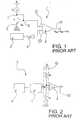
- the generator circuit 1 of the bandgap typecomprises a bipolar transistor T having its collector terminal C connected to both a first supply voltage reference Vs, via a current generator G, and the base terminal, and having its emitter terminal E connected to a second voltage reference, such as a signal ground GND.
- the base terminal Bis connected, in turn, to a first input I1 of an adder 2, whose second input I2 is connected to the cascade of a voltage VT generator 3 and a scale reducer 4 for a coefficient K.
- V BGV BE + K*V T where the value of coefficient K is selected to minimize the dependence of the generated voltage V BG on temperature.
- the generator circuit 1 of the bandgap typecomprises first N1 and second N2 bipolar transistors, first R1 and second R2 resistive elements, and a current mirror circuit 5 plus a feedback network RR.
- the bipolar transistors, N1 and N2have their base terminals B1 and B2 connected together to form an output terminal O1 of the circuit 1, and their collector terminals C1 and C2 connected to said current mirror 5.
- the first transistor N1moreover, has its emitter terminal E1 connected to a circuit node X via the first resistive element R1.
- This circuit node Xis connected to the emitter terminal E2 of the second transistor N2 and to the second voltage reference GND via the second resistive element R2.
- the feedback network RRis connected between the collector terminal C2 and the base terminal B2 of the second transistor N2.
- the feedback network RRmay simply comprise a wire lead 6, as shown in Figure 1A, or be formed of a further bipolar transistor NR having its base terminal BR connected to the collector terminal C2, its emitter terminal ER connected to the base terminal B2, and its collector terminal CR connected to the first supply voltage reference Vs, as shown in Figure 1B.
- a so-called bandgap voltage signal V BGis, therefore, obtained at the output terminal O1 which is equal to the sum of the base-emitter voltage V BE plus the voltage V'. All this according to theoretical relation (1).
- the constant Kis only dependent on the ratio of the resistive elements R1 and R2, and on the ratio of the areas of the transistors N1 and N2, and accordingly, can be selected to make the bandgap output voltage V BG as much as possible independent of temperature.
- the bandgap voltage V BG obtained in this wayis usually a constant quantity for all silicon processes and its value is 1.25V.
- the detection circuit 7 shown thereincomprises a generating circuit 1 of the badgap type which supplies a constant reference voltage signal V BG and is connected to a first inverting (-) input of a comparator 8.
- the circuit 7further comprises a trigger circuit 9 connected ahead of the generator 1.
- a second non-inverting (+) input of the comparator 8is connected to the first supply voltage reference Vs by a resistive divider 10 which comprises first R3 and second R4 resistive elements.
- the first resistive element R3is connected between the first supply voltage reference Vs and the non-inverting (+) input terminal of the comparator 8, while the second resistive element R4 is connected between that terminal and the second voltage reference GND.
- the output terminal O2 of the comparator 8is the output terminal of the circuit 7.
- the first point of operationis, however, an unstable one and a small variation in the conditions of equilibrium would be sufficient to bring the whole circuit to the second point of operation, which is the one sought.
- This functionis served by the trigger circuit 9 introducing these small variations into the conditions of operation and biasing the generating circuit 1 toward the point of operation at 1.25V.
- the detection circuit 7compares a reference voltage value of 1.25V to the value of the supply voltage, as conveniently reduced by a scale factor through the resistive divider 10.
- the trigger circuit 9 included in the supply voltage drop detecting circuit 7must remain active all the time if the device is to operate properly. This may represent a big problem, especially in low-consumption circuit applications.
- the underlying technical problem of this inventionis to provide a circuit for generating a reference voltage and detecting a drop in a supply voltage, which has such constructional and functional features as to enable both functions to be implemented in a simple and compact single structure, and can overcome the limitations and/or drawbacks with which prior art circuits have been beset.
- the solutive idea on which the present invention standsis one of using a single structure of the bandgap type to both generate a reference voltage and detect a drop in a supply voltage, which structure can be switched automatically between these two functions.
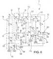
- FIG. 11generally shown at 11 is the circuit of this invention for generating a reference voltage and detecting a drop in a supply voltage.
- the circuit 11comprises a threshold comparator 12 having an input terminal IN and an output terminal OUT.
- the input terminal IN of the comparator 12is connected to a first circuit node X1, and the output teerminal OUT thereof is connected to the input terminal of a buffer block 13 having first DO and second AO output terminals.
- the first circuit node X1is a midpoint of a resistive divider 14 connected between a first supply voltage reference Vs and a second voltage reference such as a signal ground GND.
- the resistive divider 14comprises, in series, a first resistive element R3 connected between the first supply voltage reference Vs and the first circuit node X1, a second resistive element R4 connected between the first circuit node X1 and a second circuit node X2, and a third resistive element R5 connected between the second circuit node X2 and the second voltage reference GND.
- a current generator CG1Also connected to the circuit node X1, between the node X1 and the second voltage reference GND, is a current generator CG1 which is controlled by a signal generated on the second output terminal Ao of the buffer block 13.
- the overall gain G of the comparator 12is negative, i.e., when V IN is below V TH , V OUT is positive, and when V IN is above V TH , V OUT is negative.
- the threshold comparator 12can be embodied by a bandgap type of structure as shown in Figure 4, for example.
- the comparator 12comprises first N1 and second N2 bipolar transistors, first R1 and second R2 resistive elements, and a current-mirror biasing circuit 15.
- the bipolar transistors N1 and N2have their base terminals B1 and B2 connected together and to the circuit node X1, while also forming the input terminal IN, and their collector terminals C1 and C2 connected to the current mirror 15.
- the collector terminal C2 of the second transistor N2is the output terminal OUT of the comparator 12.
- the first transistor N1has its emitter terminal E1 connected to a third circuit node X3 via the first resistive element R1.
- This circuit node X3is connected to the emitter terminal E2 of the second transistor N2 and to the second voltage reference GND via the second resistive element R2.
- the bandgap voltage VBGis the same as the threshold voltage of the comparator 12, and is of 1.25V for all silicon processes.
- the generating circuit of the bandgap type which embodies the comparator 12is characterized by the output voltage V OUT switching to a low value as the input voltage VIN exceeds the internal threshold value V BG .
- This input voltage VINis, however, proportional to the supply voltage Vs according to a coefficient which is defined by the resistive divider consisting of the resistors R3 and R4 alone.
- the voltage at the first circuit node X1would be less than the threshold voltage V BG , thereby raising the output voltage of the comparator 12, and hence, the voltage at the first output terminal DO of the buffer block 13. Under these conditions, the switch SW would be closed and the resistor R5 shorted to ground GND.
- the blockcomprising the transistors N1 and N2 and resistors R1 and R2 has the behavior of a comparator whose outputs are the collector currents of the transistors N1 and N2, while the switching voltage is actually the bandgap voltage V BG .
- V UVH( 1 + R3/R4) * V BG
- the switchingis speeded up by the positive feedback introduced by the resistor R5 and by the switch SW being open.
- This positive feedbackoriginates a hysteresis phenomenon which prevents intermittent oscillations at the output terminal DO in the event that the supply voltage is not fully stabilized.
- V HYR3 ⁇ R5 R4 ⁇ (R4+R5) ⁇ V BG
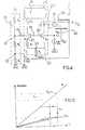
- Figure 5shows the waveforms of the bandgap voltage V BG and the voltage V DO at the output terminal DO of the buffer block 13 as a function of the supply voltage Vs.
- the output OUT of the bandgap circuit forming the comparator 12is cut off from the input IN by a negative feedback introduced by the circuit loop comprising the buffer block 13 and current generator CG1.
- This loopwould be open at lower supply voltages than the threshold value V UVH given by formula (4); under this condition, the voltage at the first circuit node X1 is proportional to the supply voltage linearly therewith.
- the feedback loopwould instead be closed when the supply voltage Vs rises above the value of the voltage V UVH ; under this condition, the voltage at the circuit node X1 is held firmly at the value of the bandgap voltage VBG by the current tapped off by the generator CG1 under control by the signal present on the second output terminal AO of the buffer block 13.
- a circuitwhich can generate a stable reference voltage equal to V BG and detect a drop in the supply voltage, signalling it by means of the voltage V DO which appears at the first: output terminal DO of the buffer block 13.
- the current mirror 15is formed of a pair of p-channel MOS transistors P1 and P2, respectively having their source terminals S1 and S2 connected to the first supply voltage reference Vs and their gate terminals G1 and G2 connected to each other.
- the transistor P1has its drain terminal D1 connected to the gate terminal G1 and the collector terminal C1 of the first bipolar transistor N1.
- the transistor P2has its drain terminal D2 connected to the collector terminal C2 of the second bipolar transistor N2, which forms the output terminal OUT of the comparator 12.
- the buffer block 13is comprised of a further p-channel MOS transistor P3, an n-channel MOS transistor N4, and a pair of resistive elements R6 and R7.
- the transistor P3has its source terminal connected to the first supply voltage reference Vs, its gate terminal G3 connected to the output terminal OUT, and its drain terminal D3 connected to a fourth circuit node X4.
- the gate terminal G3 of the transistor P3is the input terminal of the buffer block 13.
- the fourth circuit node X4is connected to the second voltage reference GND via the resistor R6, and is connected to the gate terminal G4 of the transistor N4, which has its source terminal connected to the second voltage reference GND and its drain terminal connected to the first supply voltage reference Vs via the resistor R7.
- the drain terminal D4 of the transistor N4is the first output terminal DO of the buffer block 13, while the fourth circuit node X4 is the second output terminal AO of the buffer block 13.
- This output terminal AOis connected to the generator CG1 formed of a further n-channel MOS transistor N5.
- the transistor N5has its gate terminal G5 connected to the fourth circuit node X4, its drain terminal D5 connected to the input terminal IN of the comparator 12, and its source terminal S5 connected to the second voltage reference GND.
- the switch SWis formed of a further n-channel MOS transistor N6 having its source terminal S6 connected to the second voltage reference GND, its drain terminal D6 connected to the second circuit node X2, and its gate terminal G6 connected to the first output terminal DO of the buffer block 13.
- the transistor N4whose function is that of holding the voltage present on the output terminal DO at a low value, behaves as a switch.
- circuit node DOswitches to a supply voltage value Vs above the value at which the transistor N3 begins to draw current from the first node X1.
- ⁇ V[V UVH - V GS6 (I R4 )] ⁇ R3 R7 ⁇ W5 ⁇ L4 W4 ⁇ L5
- the real detection threshold obtained by means of the circuit 11 of this inventionwill be the closer to the theoretical threshold V UVH sought, the smaller is the value of the voltage difference ⁇ V from formula (6).
- the supply voltage rejectionis of 90 dB up to a frequency of 100 Hz, to drop by 20 dB/decade up to a frequency of 1 MHz, and eventually retain a steady value of 10 dB at frequencies above that.
Landscapes
- Engineering & Computer Science (AREA)
- Physics & Mathematics (AREA)
- Power Engineering (AREA)
- Microelectronics & Electronic Packaging (AREA)
- Electromagnetism (AREA)
- General Physics & Mathematics (AREA)
- Radar, Positioning & Navigation (AREA)
- Automation & Control Theory (AREA)
- Nonlinear Science (AREA)
- Control Of Electrical Variables (AREA)
- Measurement Of Current Or Voltage (AREA)
- Direct Current Feeding And Distribution (AREA)
Description
W4/L4 = 100u/3u W5/L5 = 20u/20u.
IA = 350 µa A = 0.40 mm2where, IA is the current drain and A is the area occupied.
IA = 200 µa A = 0.20 mm2that is, values nearly halved from those of conventionalcircuits, for the same circuit accuracy as the processparameters in its making vary.
Claims (13)
- A circuit for generating a reference voltage anddetecting a drop in a supply voltage, which circuitcomprises at least one threshold comparator (12) having aninput terminal (IN) and an output terminal, and a voltagedivider (14) connected between a first supply voltagereference (Vs) and a second voltage reference (GND) andconnected to the input terminal (IN) of the comparator(12), characterized in that the output terminal (OUT) ofsaid comparator (12) is connected to the input terminal(IN) through at least one controlled negative feedbacknetwork comprising at least one current generator (CG1),and further characterized in that the output terminal (OUT)is coupled to a switch (N4) that controls a signalindicating a drop in the supply voltage.
- A circuit according to Claim 1, characterized in thatsaid at least one feedback network comprises a buffer block(13) having an input terminal connected to said comparator(12) and a first output terminal (DO) connected to a switch(SW) which is connected between a circuit node (X2) of saidvoltage divider (14) and the second voltage reference(GND).
- A circuit according to Claim 2, characterized in thatsaid current generator (CG1) is connected between the inputterminal (IN) of the comparator (12) and the second voltagereference (GND) and is controlled by a signal generated ona second output terminal (AO) of the buffer block (13).
- A circuit according to Claim 1, characterized in thatsaid comparator (12) is of the bandgap type and connectedbetween the first supply voltage reference (Vs) and the second voltage reference (GND).
- A circuit according to Claim 2, characterized in thatsaid voltage divider (14) comprises, in series, at leastfirst (R3), second (R4) and third (R5) resistive elements,with the first resistive element (R3) being connectedbetween the first supply voltage reference (Vs) and a firstcircuit node (X1) connected to the input terminal (IN) ofsaid comparator (12), the second resistive element (R4)connected between said first circuit node (X1) and saidcircuit node (X2), and the third resistive element (R5)connected between said circuit node (X2) and the secondvoltage reference (GND).
- A circuit according to Claim 4, wherein the buffer block(13) comprises a series of a first MOS transistor (P3) anda first resistive element (R6), and a series of a secondMOS transistor (N4) and a second resistive element (R7),which are connected between the supply voltage reference(Vs) and the second voltage reference (GND), characterizedin that the drain terminal (D3) of the first MOS transistor(P3) is connected to the gate terminal (G4) of the secondMOS transistor (N4).
- A circuit according to Claim 6, characterized in thatsaid current generator (CG1) comprises a further MOStransistor (N5), and that said second transistor (N4) has awidth-to-length ratio (W/L) much higher than the width-to-lengthratio (W/L) of said further transistor (N5).
- A circuit according to Claims 2 and 6, characterized inthat said switch (SW) comprises a MOS transistor (N6)having its gate terminal connected to the first outputterminal (DO) of the buffer block (13), its drain terminal(D6) connected to the circuit node (X2) of said resistivedivider (14), and its source terminal connected to thesecond voltage reference (GND).
- A method of generating a reference voltage andsimultaneously detecting a drop in a supply voltage to anelectronic circuit (1) which is connected between a firstsupply voltage reference (Vs) and a second voltagereference (GND) through a voltage divider (14), andcomprises a single threshold comparator (12) having aninput terminal (IN) and an output terminal (OUT) connectedto each other through at least one controlled negativefeedback network which includes a buffer block (13) havingan output terminal (DO) used to indicate the drop in thesupply voltage, the buffer block (13) connected betweensaid output terminal (OUT) and a current generator (CG1)connected between the input terminal (IN) of the comparator(12) and the second voltage reference (GND) and beingcontrolled by a signal (VAO) generated on an outputterminal (AO) of the comparator (12), the voltage (VIN) atthe input terminal being held constant by tapping offexcess current being supplied to said input terminal (IN)when the voltage at the input terminal (IN) of thecomparator (12) exceeds the treshold (VBG) of thecomparator, in order to thereby obtain a stable referencevoltage.
- A method according to Claim 9, characterized in thatsaid comparator (12) is of the bandgap type and connectedbetween the first supply voltage reference (Vs) and thesecond voltage reference (GND).
- A method according to Claim 10, characterized in that aswitch (SW) is provided in the feedback line, and that:the feedback network switch (SW) closesautomatically as the input voltage (VIN) exceeds athreshold voltage value (VBG) of the comparator(12), thereby generating a reference voltage (VIN) ;andsaid switch (SW) opens automatically as the inputvoltage (VIN) drops below the threshold voltagevalue (VBG), thereby indicating a drop in thesupply voltage (Vs).
- A method according to Claim 11, characterized in that,during the switch (SW) opening, a hysteresis phenomenon isbrought about which is effective to prevent oscillations ofa voltage (VDO) on the output terminal (DO) of the bufferblock (13) in the presence of a supply voltage which isless than fully stabilized.
- A method according to Claim 12, characterized in thatsaid switch (SW) is controlled by the signal present on theoutput terminal (DO) of the buffer block (13), whichswitches from a low value when the voltage at the inputterminal (IN) of the comparator (12) is higher than aninternal threshold value (VBG) over to a high value whenthe voltage at the input terminal (IN) is lower than theinternal threshold value (VBG).
Priority Applications (4)
| Application Number | Priority Date | Filing Date | Title |
|---|---|---|---|
| EP95830111AEP0733959B1 (en) | 1995-03-24 | 1995-03-24 | Circuit for generating a reference voltage and detecting an undervoltage of a supply voltage and corresponding method |
| DE69521287TDE69521287T2 (en) | 1995-03-24 | 1995-03-24 | Circuit arrangement for generating a reference voltage and detection of a supply voltage drop and associated method |
| US08/622,459US5747978A (en) | 1995-03-24 | 1996-03-22 | Circuit for generating a reference voltage and detecting an under voltage of a supply and corresponding method |
| JP8068815AJPH08272470A (en) | 1995-03-24 | 1996-03-25 | Circuit for generating reference voltage and detecting undervoltage of power supply voltage, and corresponding method |
Applications Claiming Priority (1)
| Application Number | Priority Date | Filing Date | Title |
|---|---|---|---|
| EP95830111AEP0733959B1 (en) | 1995-03-24 | 1995-03-24 | Circuit for generating a reference voltage and detecting an undervoltage of a supply voltage and corresponding method |
Publications (2)
| Publication Number | Publication Date |
|---|---|
| EP0733959A1 EP0733959A1 (en) | 1996-09-25 |
| EP0733959B1true EP0733959B1 (en) | 2001-06-13 |
Family
ID=8221878
Family Applications (1)
| Application Number | Title | Priority Date | Filing Date |
|---|---|---|---|
| EP95830111AExpired - LifetimeEP0733959B1 (en) | 1995-03-24 | 1995-03-24 | Circuit for generating a reference voltage and detecting an undervoltage of a supply voltage and corresponding method |
Country Status (4)
| Country | Link |
|---|---|
| US (1) | US5747978A (en) |
| EP (1) | EP0733959B1 (en) |
| JP (1) | JPH08272470A (en) |
| DE (1) | DE69521287T2 (en) |
Cited By (1)
| Publication number | Priority date | Publication date | Assignee | Title |
|---|---|---|---|---|
| CN106443146A (en)* | 2016-09-12 | 2017-02-22 | 浙江中控技术股份有限公司 | Master-slave system fault detection and processing system |
Families Citing this family (29)
| Publication number | Priority date | Publication date | Assignee | Title |
|---|---|---|---|---|
| KR19980064252A (en)* | 1996-12-19 | 1998-10-07 | 윌리엄비.켐플러 | Low Dropout Voltage Regulator with PMOS Pass Element |
| EP0863611B1 (en)* | 1997-03-04 | 2003-08-06 | STMicroelectronics S.r.l. | A short-circuit detecting device |
| FR2772155B1 (en)* | 1997-12-10 | 2000-02-11 | Matra Mhs | DEVICE FOR GENERATING A CONTINUOUS REFERENCE VOLTAGE |
| US6147883A (en)* | 1998-11-16 | 2000-11-14 | Power Integrations, Inc. | Output feedback and under-voltage detection |
| FR2801678B1 (en)* | 1999-11-30 | 2002-02-01 | St Microelectronics Sa | HIGH VOLTAGE DETECTION DEVICE |
| US6222399B1 (en) | 1999-11-30 | 2001-04-24 | International Business Machines Corporation | Bandgap start-up circuit |
| US6172495B1 (en)* | 2000-02-03 | 2001-01-09 | Lsi Logic Corporation | Circuit and method for accurately mirroring currents in application specific integrated circuits |
| US6957278B1 (en)* | 2000-06-28 | 2005-10-18 | Cypress Semiconductor Corp. | Reference -switch hysteresis for comparator applications |
| US7136592B2 (en)* | 2000-08-11 | 2006-11-14 | International Business Machines Corporation | Self aligning optical detector |
| JP2002270768A (en)* | 2001-03-08 | 2002-09-20 | Nec Corp | Cmos reference voltage circuit |
| US6580593B2 (en) | 2001-03-14 | 2003-06-17 | Power Integrations, Inc. | Method and apparatus for fault condition protection of a switched mode power supply |
| AU2003241234A1 (en)* | 2002-05-28 | 2003-12-12 | Igor Anatolievich Abrosimov | Reference voltage generator for logic elements providing stable and predefined gate propagation time |
| KR100571637B1 (en)* | 2003-10-30 | 2006-04-17 | 주식회사 하이닉스반도체 | Supply voltage supply in delay locked loop |
| US7440249B2 (en)* | 2005-03-30 | 2008-10-21 | Silicon Laboratories, Inc. | Undervoltage detection circuit |
| US7215185B2 (en)* | 2005-05-26 | 2007-05-08 | Texas Instruments Incorporated | Threshold voltage extraction for producing a ramp signal with reduced process sensitivity |
| US20070296384A1 (en)* | 2006-06-26 | 2007-12-27 | Semiconductor Components Industries, Llc. | Method of forming a feedback network and structure therefor |
| JP4710739B2 (en)* | 2006-06-30 | 2011-06-29 | 株式会社デンソー | Load disconnection detection circuit |
| US20080150594A1 (en)* | 2006-12-22 | 2008-06-26 | Taylor Stewart S | Start-up circuit for supply independent biasing |
| GB0806491D0 (en)* | 2008-04-10 | 2008-05-14 | Rolls Royce Plc | A method and system for electrical power generation |
| US7609049B1 (en)* | 2008-05-28 | 2009-10-27 | Vimicro Corporation | Accurate scan-mode voltage detection circuit |
| US8354878B2 (en) | 2009-12-23 | 2013-01-15 | Stmicroelectronics Design And Application S.R.O. | Integrated electronic device with reference voltage signal generation module and UVLO logic signal generation module |
| US9086434B1 (en)* | 2011-12-06 | 2015-07-21 | Altera Corporation | Methods and systems for voltage reference power detection |
| US8922218B2 (en)* | 2011-12-28 | 2014-12-30 | O2Micro Inc | Detection circuits for batteries |
| JP5896805B2 (en)* | 2012-03-27 | 2016-03-30 | キヤノン株式会社 | Power supply device and display device |
| CN102944717B (en)* | 2012-11-14 | 2015-09-16 | 江苏惠通集团有限责任公司 | Voltage check device and method |
| JP6136480B2 (en)* | 2013-04-03 | 2017-05-31 | トヨタ自動車株式会社 | Bandgap reference circuit |
| US11271566B2 (en)* | 2018-12-14 | 2022-03-08 | Integrated Device Technology, Inc. | Digital logic compatible inputs in compound semiconductor circuits |
| US11199565B1 (en)* | 2020-07-17 | 2021-12-14 | Novatek Microelectronics Corp. | Undervoltage detection circuit |
| CN115309219B (en)* | 2022-08-03 | 2024-02-02 | 上海艾为电子技术股份有限公司 | Start-up completion indication signal circuit, signal forming method and chip |
Family Cites Families (8)
| Publication number | Priority date | Publication date | Assignee | Title |
|---|---|---|---|---|
| US3852679A (en)* | 1972-12-26 | 1974-12-03 | Rca Corp | Current mirror amplifiers |
| US4234841A (en)* | 1979-02-05 | 1980-11-18 | Rca Corporation | Self-balancing bridge network |
| US4317054A (en)* | 1980-02-07 | 1982-02-23 | Mostek Corporation | Bandgap voltage reference employing sub-surface current using a standard CMOS process |
| NL8001558A (en)* | 1980-03-17 | 1981-10-16 | Philips Nv | POWER STABILIZER BUILT UP WITH ENRICHMENT TYPE FIELD-EFFECT TRANSISTOR. |
| WO1990006547A1 (en)* | 1988-12-05 | 1990-06-14 | Alcatel N.V. | Voltage transducer |
| US5084665A (en)* | 1990-06-04 | 1992-01-28 | Motorola, Inc. | Voltage reference circuit with power supply compensation |
| FR2669783A1 (en)* | 1990-11-27 | 1992-05-29 | Valeo Equip Electr Moteur | DEVICE FOR REGULATING THE CHARGING VOLTAGE OF A BATTERY BY AN ALTERNATOR. |
| KR950010284B1 (en)* | 1992-03-18 | 1995-09-12 | 삼성전자주식회사 | Reference voltage generating circuit |
- 1995
- 1995-03-24EPEP95830111Apatent/EP0733959B1/ennot_activeExpired - Lifetime
- 1995-03-24DEDE69521287Tpatent/DE69521287T2/ennot_activeExpired - Fee Related
- 1996
- 1996-03-22USUS08/622,459patent/US5747978A/ennot_activeExpired - Lifetime
- 1996-03-25JPJP8068815Apatent/JPH08272470A/enactivePending
Cited By (1)
| Publication number | Priority date | Publication date | Assignee | Title |
|---|---|---|---|---|
| CN106443146A (en)* | 2016-09-12 | 2017-02-22 | 浙江中控技术股份有限公司 | Master-slave system fault detection and processing system |
Also Published As
| Publication number | Publication date |
|---|---|
| DE69521287D1 (en) | 2001-07-19 |
| JPH08272470A (en) | 1996-10-18 |
| US5747978A (en) | 1998-05-05 |
| DE69521287T2 (en) | 2002-05-02 |
| EP0733959A1 (en) | 1996-09-25 |
Similar Documents
| Publication | Publication Date | Title |
|---|---|---|
| EP0733959B1 (en) | Circuit for generating a reference voltage and detecting an undervoltage of a supply voltage and corresponding method | |
| EP0419093B1 (en) | Current sensing circuit | |
| US5004970A (en) | Device and a process for detecting current flow in a MOS transistor | |
| US5059820A (en) | Switched capacitor bandgap reference circuit having a time multiplexed bipolar transistor | |
| EP0360333A2 (en) | Temperature threshold sensing circuit | |
| EP0194031A1 (en) | CMOS bandgap reference voltage circuits | |
| US6445305B2 (en) | CMOS low battery voltage detector | |
| US4701639A (en) | Threshold detector circuit and method | |
| KR20000075637A (en) | Current-limit circuit | |
| US4647840A (en) | Current mirror circuit | |
| US4612513A (en) | Differential amplifier | |
| EP0343731B1 (en) | Unity-gain current-limiting circuit | |
| EP0483526B1 (en) | A current threshold detector circuit | |
| US6316995B1 (en) | Input stage for constant gm amplifier circuit and method | |
| JP2643133B2 (en) | Stabilized power supply circuit | |
| US5402011A (en) | Current source circuit | |
| JP2645596B2 (en) | Voltage detection circuit | |
| CN118501532B (en) | Multifunctional detection circuit | |
| SU1046747A1 (en) | Dc voltage stabilizer | |
| JP2656297B2 (en) | Wind circuit | |
| JPH04322511A (en) | Hysteresis comparator circuit | |
| JPH0742145Y2 (en) | Voltage monitoring circuit | |
| RU2006060C1 (en) | Current source | |
| JPS63219223A (en) | Drive circuit | |
| JPS62241427A (en) | Light input semiconductor switch circuit |
Legal Events
| Date | Code | Title | Description |
|---|---|---|---|
| PUAI | Public reference made under article 153(3) epc to a published international application that has entered the european phase | Free format text:ORIGINAL CODE: 0009012 | |
| AK | Designated contracting states | Kind code of ref document:A1 Designated state(s):DE FR GB IT | |
| 17P | Request for examination filed | Effective date:19970321 | |
| RAP3 | Party data changed (applicant data changed or rights of an application transferred) | Owner name:STMICROELECTRONICS S.R.L. Owner name:CO.RI.M.ME. CONSORZIO PER LA RICERCA SULLA MICROEL | |
| 17Q | First examination report despatched | Effective date:19990913 | |
| GRAG | Despatch of communication of intention to grant | Free format text:ORIGINAL CODE: EPIDOS AGRA | |
| GRAG | Despatch of communication of intention to grant | Free format text:ORIGINAL CODE: EPIDOS AGRA | |
| GRAH | Despatch of communication of intention to grant a patent | Free format text:ORIGINAL CODE: EPIDOS IGRA | |
| GRAH | Despatch of communication of intention to grant a patent | Free format text:ORIGINAL CODE: EPIDOS IGRA | |
| GRAA | (expected) grant | Free format text:ORIGINAL CODE: 0009210 | |
| ITF | It: translation for a ep patent filed | ||
| AK | Designated contracting states | Kind code of ref document:B1 Designated state(s):DE FR GB IT | |
| ET | Fr: translation filed | ||
| REF | Corresponds to: | Ref document number:69521287 Country of ref document:DE Date of ref document:20010719 | |
| REG | Reference to a national code | Ref country code:GB Ref legal event code:IF02 | |
| PLBE | No opposition filed within time limit | Free format text:ORIGINAL CODE: 0009261 | |
| STAA | Information on the status of an ep patent application or granted ep patent | Free format text:STATUS: NO OPPOSITION FILED WITHIN TIME LIMIT | |
| 26N | No opposition filed | ||
| PGFP | Annual fee paid to national office [announced via postgrant information from national office to epo] | Ref country code:DE Payment date:20040305 Year of fee payment:10 | |
| PG25 | Lapsed in a contracting state [announced via postgrant information from national office to epo] | Ref country code:IT Free format text:LAPSE BECAUSE OF NON-PAYMENT OF DUE FEES;WARNING: LAPSES OF ITALIAN PATENTS WITH EFFECTIVE DATE BEFORE 2007 MAY HAVE OCCURRED AT ANY TIME BEFORE 2007. THE CORRECT EFFECTIVE DATE MAY BE DIFFERENT FROM THE ONE RECORDED. Effective date:20050324 | |
| PG25 | Lapsed in a contracting state [announced via postgrant information from national office to epo] | Ref country code:DE Free format text:LAPSE BECAUSE OF NON-PAYMENT OF DUE FEES Effective date:20051001 | |
| PGFP | Annual fee paid to national office [announced via postgrant information from national office to epo] | Ref country code:GB Payment date:20060223 Year of fee payment:12 | |
| PGFP | Annual fee paid to national office [announced via postgrant information from national office to epo] | Ref country code:FR Payment date:20060329 Year of fee payment:12 | |
| GBPC | Gb: european patent ceased through non-payment of renewal fee | Effective date:20070324 | |
| REG | Reference to a national code | Ref country code:FR Ref legal event code:ST Effective date:20071130 | |
| PG25 | Lapsed in a contracting state [announced via postgrant information from national office to epo] | Ref country code:GB Free format text:LAPSE BECAUSE OF NON-PAYMENT OF DUE FEES Effective date:20070324 | |
| PG25 | Lapsed in a contracting state [announced via postgrant information from national office to epo] | Ref country code:FR Free format text:LAPSE BECAUSE OF NON-PAYMENT OF DUE FEES Effective date:20070402 |